Embed Size (px)
Citation preview

IEEE JOURNAL OF SOLID-STATE CIRCUITS, VOL. 46, NO. 12, DECEMBER 2011 3047
A SAW-Less GSM/GPRS/EDGE Receiver Embeddedin 65-nm SoC
Chi-Yao Yu, Member, IEEE, Ivan Siu-Chuang Lu, Member, IEEE, Yen-Horng Chen, Lan-Chou Cho,Chih-Hao Eric Sun, Chih-Chun Tang, Hsiang-Hui Chang, Wen-Chang Lee, Member, IEEE, Sheng-Jui Huang,
Tzung-Han Wu, Member, IEEE, Chinq-Shiun Chiu, and George Chien, Senior Member, IEEE
Abstract—A quad-band GSM/GPRS/EDGE receiver, imple-mented in 65 nm CMOS, complies with the ETSI standard withoutthe need of external SAW filters. By exploring the properties ofpassive mixers and current-mode operation from RF to baseband,the receiver can achieve a SAW-filter-like selectivity with inex-pensive on-chip components such as resistors and capacitors. Inaddition, to alleviate the linearity bottleneck at the LNA inputstage, Class-AB self-bias LNTA is employed to break the conven-tional trade-off’s among NF, linearity and power consumption.For single-to-differential conversion, external LC-CL baluns(instead of on-chip baluns) are used to balance the on-chip die andexternal BOM cost. This receiver solution is embedded as a partof a cellular phone SoC and achieves 110 dBm sensitivity,�1 dBm Out-of-Band �� �� and consumes 58.9 mA. In FTA
test, the receiver passes out-of-band blocker test with � dBmargin.
Index Terms—Blocker detection, class-AB, current-mode,dynamic range, GSM, impedance transformation, receiver,SAW-less.
I. INTRODUCTION
O VER the last decade, demands of mobile communica-tion have seen an explosive growth where the coverage of
second-generation (2G) mobile communication standard suchas GSM has reached 1.5 billion people across more than212 countries [1]. Many of these are emerging countries wherethe convenience of wireless communication can greatly enrichpeople’s lives in different ways. To realize this, significant ef-forts have been made towards increasing integration and re-ducing the bill of material (BOM) for mobile devices, whichin turn reduce costs of ownership.
In recent years, an increasing number of radios with CMOSimplementation and high level of integration (e.g., single-chipphone) [2] have been introduced in the market. To meet the GSMstandard, external filters are generally used to filter blocker orinterference signals in receivers (RX) and to reduce noise in
Manuscript received April 13, 2011; revised July 31, 2011; accepted Au-gust 06, 2011. Date of publication October 06, 2011; date of current versionNovember 23, 2011. This paper was approved by Guest Editor Yorgos Palaskas.
C.-Y. Yu, L.-C. Cho, C.-H. E. Sun, C.-C. Tang, H.-H. Chang, T.-H. Wu,and C.-S. Chiu are with MediaTek Inc., Hsinchu, Taiwan 30078 (e-mail:[email protected]; [email protected]; [email protected]; [email protected]; [email protected]; [email protected]; [email protected]).
I. S.-C. Lu and G. Chien are with MediaTek USA Inc., San Jose, CA 95134USA (e-mail: Ivan.lu@ mediatek.com; [email protected]).
Y.-H. Chen and W.-C. Lee are with MediaTek Inc., Austin, TX 78730 USA(e-mail: [email protected]; [email protected]).
S.-J. Huang is with MediaTek Inc., Woburn, MA 01801-1130 USA (e-mail:[email protected]).
Digital Object Identifier 10.1109/JSSC.2011.2166657
the RX band of transmitters (TX). With innovative TX archi-tectures and circuits, external transmit filters have largely beeneliminated [3], while receive filters are still present. Due to thestringent filtering requirements, these RX filters are generallymade with surface acoustic wave (SAW) technology. Not onlydo these filters reduce the RX sensitivity due to filter insertionloss, but they make up a big part of the external BOM cost for thewireless system. Therefore, for high-volume application, signif-icant cost savings offered by a SAW-filter-less solution is a gen-uine advantage and a key product differentiator.
In wireless radios, the received spectrum typically consistsof a weak desired signal accompanied by interferers that canbe much stronger in power at various offset frequencies. Forconventional quad-band GSM RXs, the received signal passesthrough the antenna switch module (ASM), followed by fourexternal SAW filters before entering the four on-chip low noiseamplifiers (LNAs), as shown in Fig. 1(a). These filters rejectstrong out-of-band (OOB) blockers to minimize their negativeeffects on the RXs. As the name suggests, SAW-less RX elimi-nates the need for SAW filters and improves the RX sensitivity.In addition, as shown in Fig. 1(b), only two baluns and twoon-chip LNAs are required due to the close proximity of theGSM frequencies. By removing the SAW filter and having asmaller ASM with only two RX ports, the external BOM re-quired for a GSM phone can be reduced by up to 50%. This isof great importance for a high-volume, low-cost market like the2G cellular phone market today.
In this paper, Section II introduces the GSM specificationsand the unique design challenges for a SAW-less receiver.Sections III–V describe the techniques and circuit imple-mentations which break the conventional wisdom of RXdesign, namely, noise, linearity, and power consumption trade-offs. Measurement results are included in Section VI, whileSection VII concludes the paper.
II. GSM SAW-LESS RECEIVER DESIGN CHALLENGES
A. GSM Specifications
Fig. 2 shows the GSM900/PCS receive spectrums definedin the GSM specifications. In addition to the adjacent channelinterference signals within the GSM bands, it also requiresa radio to successfully receive a desired signal at 99 dBmwhile withstanding a 0-dBm continuous wave (CW) blockersignal at 20 MHz away for 850/900 bands or 80 MHz awayfor DCS/PCS bands. A typical SAW filter provides at least20-dB rejection at 20-MHz offset, which attenuates the 0-dBmblocker to roughly the same level as the 3-MHz adjacentchannel interference (ACI). Without the protection of the SAW
0018-9200/$26.00 © 2011 IEEE

3048 IEEE JOURNAL OF SOLID-STATE CIRCUITS, VOL. 46, NO. 12, DECEMBER 2011
Fig. 1. (a) Conventional SAW-based receiver front-end. (b) SAW-less receiverfront-end.
Fig. 2. PCS/GSM900 receive spectrums defined in the GSM specification.
filter, conventional RX will suffer severe signal desensitizationand blocker induced noise that would not normally be there.
B. Dynamic Range Versus Power Versus Noise
In a SAW-less RX, the 0-dBm OOB blocking signal must bereceived simultaneously with 99 dBm desired signal. The re-quired SNR to properly demodulate the GSM signal is around6 dB; this translates to 100–dB dynamic range requiredfor the RX. To overcome the linearity limitation due to the0-dBm blocker, a highly selective frequency down-conversion
interface is introduced. By employing passive mixers followedby a current-mode low-pass filter, this technique creates a lowimpedance node at the low-noise transconductance amplifier(LNTA) output at the blocker frequency to reduce the voltageswing and effectively filters the blocker energy before enteringthe transimpedance amplifier (TIA). It successfully removeslinearity bottlenecks at the LNTA output and TIA input in con-ventional RX. A detailed analysis can be found in Section III.
While linearity bottlenecks in other parts of the RX have beenremoved, the LNTA still needs to process the 0-dBm blockersignal as it enters the RX input. With the matching gain, thesingle-ended blocker swing at LNTA input ports can reach1 . To keep the LNTA linear over such a large inputrange, a Class-AB adaptive bias is introduced. This LNTA,under typical condition, functions like a normal transconduc-tance amplifier. When blocker signal power increases beyond
15 dBm, the Class-AB adaptive bias action starts to providea gain boosting effect to increase the compression point.In turn, this improves the overall RX dynamic range and keepsthe power consumption low under normal conditions. Detaileddiscussion can be found in Section IV.
C. Reciprocal Mixing
In any RX, the received desired signal is mixed by the LOspectrum and down-converted to baseband frequency for fur-ther signal processing. In the same way, the adjacent channelsignal in the received spectrum is also mixed by LO phase noise(PN) and down-converted to the same baseband frequency; thisdegrades the SNR of the RX. The PN requirement of the LOsignal is given by
(1)
Based on (1), for a GSM SAW-less RX with 0 dBm blocker at20 MHz offset, 99 dBm signal, 200-kHz signal bandwidth,and 6-dB SNR, the maximum LO PN at 20-MHz offset is
158 dBc/Hz. To minimize the PN contribution to the overallRX noise floor, the actual LO PN target is set at 163 dBc/Hz.This value is around 20 dB tougher compared with a conven-tional RX where the 0-dBm OOB blockers have been rejectedby the SAW filter. In addition, spurs present in the LO spec-trum can inadvertently down-convert the blocker and furtherdegrades the SNR.
In summary, to implement a SAW-less RX successfully, thereceive signal path needs to have 100 dB dynamic range,low noise, and low power; and the LO signal also needs to beextremely pure with low PN and low spurs.
III. CURRENT-MODE RECEIVER WITH HIGHLY SELECTIVE
FREQUENCY-CONVERSION INTERFACE
A. Overview of the Current-Mode Receiver Architecture
In the conventional voltage-mode RX architecture [4]–[6], astage is often adopted between the LNA and the mixer for
noise suppression and LO-to-RF port isolation purposes. Sincethe stage usually has high input impedance, the voltage gainof the LNA is the key factor to suppress the noise from the fol-lowing stages. Typically, in GSM system, to achieve 110 dBmsensitivity, the required LNA voltage gain is usually more than
YU et al.: A SAW-LESS GSM/GPRS/EDGE RECEIVER EMBEDDED IN 65-NM SOC 3049
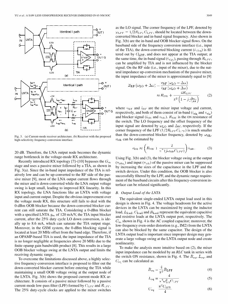
Fig. 3. (a) Current-mode receiver architecture. (b) Receiver with the proposedhigh-selectivity frequency-conversion interface.
20 dB. Therefore, the LNA output node becomes the dynamicrange bottleneck in the voltage-mode RX architecture.
Recently introduced RX topology [7]–[10] bypasses thestage and uses a passive mixer followed by a TIA, as shown inFig. 3(a). Since the in-band input impedance of the TIA is rel-atively low and can be up-converted to the RF side of the pas-sive mixer [9], most of the LNA output current flows throughthe mixer and is down-converted while the LNA output voltageswing is kept small, leading to improved RX linearity. In thisRX topology, the LNA functions like an LNTA with voltageinput and current output. Despite the obvious improvement overthe voltage mode RX, this structure still fails to deal with the0-dBm OOB blocker because the down-converted blocker cur-rent can still saturate the TIA. Considering a 0-dBm blockerwith a specified LNTA of 120 mA/V, the TIA input blockercurrent, after the 25% duty cycle LO down conversion, is ide-ally up to 8.6 mA, which can saturate the TIA output stage.Moreover, in the GSM system, the 0-dBm blocking signal islocated at least 20 MHz offset from the band edge. Therefore, ifan OPAMP-based TIA is used, the input impedance of the TIAis no longer negligible at frequencies above 20 MHz due to thefinite opamp gain bandwidth product [8]. This results in a largeOOB blocker voltage swing at the LNTA output and limits thereceiving dynamic range.
To overcome the limitations discussed above, a highly selec-tive frequency-conversion interface is proposed to filter out thedown-converted blocker current before entering the TIA whilemaintaining a small OOB voltage swing at the output node ofthe LNTA. Fig. 3(b) shows the proposed current-mode RX ar-chitecture. It consists of a passive mixer followed by a passivecurrent-mode low-pass filter (LPF) formed by and .The 25% duty-cycle clocks are applied to the mixer switches
as the LO signal. The corner frequency of the LPF, denoted by, should be located between the down-
converted blocker and in-band signal frequency. Also shown inFig. 3(b) are the in-band and OOB blocker signal flows. On thebaseband side of the frequency conversion interface (i.e., inputof the TIA), the down-converted blocking current ( ) is fil-tered out by , and does not appear at the TIA output; atthe same time, the in-band signal ( ), passing through ,can be amplified by TIA and is not influenced by the blockersignal. On the RF side (i.e., input of the mixer), due to the nat-ural impedance up-conversion mechanism of the passive mixer,the input impedance of the mixer is approximately equal to [9]
(2)
where and are the mixer input voltage and current,respectively, and both of them consist of in-band ( and )and blocker signal ( and ). is the ON resistance ofthe switch. The LO frequency and the offset frequency of theinput signal are denoted by and , respectively. If thecorner frequency of the LPF ( ) is much smallerthan the down-converted blocker frequency, denoted by ,
can be estimated by
(3)
Using Fig. 3(b) and (3), the blocker voltage swing at the output( ) and input ( ) of the passive mixer can be suppressedby increasing the sizes of the capacitance in the LPF and theswitch devices. Under this condition, the OOB blocker is alsosuccessfully filtered by the LPF, and the dynamic range require-ment of the baseband circuits after this frequency-conversion in-terface can be relaxed significantly.
B. Output Load of the LNTA
The equivalent single-ended LNTA output load used in thisdesign is shown in Fig. 4. The voltage headroom for the activedevices in the LNTA can be maximized by using the inductorload, . and represent the equivalent capacitiveand resistive loads at the LNTA output port, respectively. The
shown in Fig. 4 is the AC coupled capacitor; moreover, thelow-frequency even-order distortion (e.g., IM2) from the LNTAcan also be blocked by the same capacitor. The design of theLNTA output load is important since improper design may gen-erate a large voltage swing at the LNTA output node and createnonlinearity.
To make the analysis more intuitive based on (2), the mixerinput impedance can be modeled by an RLC tank in series withthe switch ON resistance, shown in Fig. 4. The , , and
can be calculated as
(4)
(5)
(6)

3050 IEEE JOURNAL OF SOLID-STATE CIRCUITS, VOL. 46, NO. 12, DECEMBER 2011
Fig. 4. Equivalent LNTA single-ended output load and model of the mixer andLPF.
Fig. 5. (a) Equivalent model when � � � and � �. (b) Simulation resultsof � and �� ��� � (� , � , and� are 300 fF, 600 �, and 6 �,respectively, and � is set to 1.6 MHz with � of 1 �F and � of 100�).
respectively. The 3-dB bandwidth of the RLC tank in Fig. 4 is. Therefore, for the OOB blocker at frequency
, where , the impedance of the RLC tankis dominated by or for negative or positive , re-spectively. The equivalent circuits for both cases are shown inFig. 5(a).
Considering the toughest case in the ETSI GSM specificationfor RX, i.e., 20 MHz and is around 900 MHz, itis assumed that in the following analysis. In
Fig. 5(a), the inductor and, equivalently, is maximizedto prevent in-band signal loss. In addition, the -factor of theimpedance in Fig. 5(a), should also be high atsince needs to be small to minimize the blocker voltageswing as described in the previous section. Due to the compositehigh- network, if the resonant frequency of , de-noted by , is close to , then a huge voltage swing canbe generated at the LNTA output node by the received 0-dBmblocker signal. For demonstration purposes, Fig. 5(b) showsthe simulation results of and atwith different and . In the simulation, andare 900 and 20 MHz, respectively. As shown in Fig. 5(b),
is large when is close to . To achieve asmaller , the chosen should be much smallerthan . For a given , this can be achieved by using a larger
.In addition, since is directly on the blocker signal path,
its size also needs to be made sufficiently large to suppressas shown in Fig. 5(b). In fact, such choice of
and equivalently makes as an RF choke whoseimpedance is much larger than around . This allowsboth the in-band and blocker current generated by the LNTAto flow into the highly selective impedance path withoutboosting the LNTA output voltage swing.
In summary, with sufficiently large , the following equa-tion is true in the design:
(7)
where the factors of and are .
C. In-Band RF Current Gain
Besides the OOB voltage swing, the in-band RF current gain,which is the ratio between mixer input current and the LNTAoutput current, also need to be considered in the design. For thein-band signal located at frequency , where
, the impedance of the RLC tank in Fig. 4 is dominated byand its equivalent circuit is shown in Fig. 6(a). Based on the
equivalent circuit, the in-band RF current gain can beeasily calculated as
(8)
where and are the current from the LNTA and the cur-rent into the mixer, respectively. Equation (8) is valid when the
-factor of and . According to (7), theimpedance of is much larger than and the impedanceof . An optimal design can be made by gradually

YU et al.: A SAW-LESS GSM/GPRS/EDGE RECEIVER EMBEDDED IN 65-NM SOC 3051
Fig. 6. (a) In-band equivalent model. (b) Simulation results of � .
reducing to decrease the denominator in (8). This allowsfor a higher in-band RF current gain with an acceptable blockervoltage swing. To demonstrate this phenomenon, thesimulation results with different and are shown inFig. 6(b).
IV. ADAPTIVE POWER SCALING TECHNIQUES
In order to be commercially successful, the SAW-less RXmust achieve high dynamic range, low RX noise, and low LOPN while operating under the same power constraint as conven-tional SAW-based RXs. At first, such a design seems extremelydifficult given the obvious need to break the universal tradeoffsbetween linearity, noise, and power consumption in analog cir-cuit design. However, careful examination of real-life channelconditions reveals that the SAW-less RX only needs to tolerate0-dBm blockers on very rare occasions. This knowledge enablesthe use of self-adaptive circuits to scale the RX performancewith the real-time blocker profile and drastically improve theoverall power efficiency.
A. Class-AB Self-Biased LNTA
The LNTA is the first stage of a typical RX, and its mainpurpose is to provide low noise signal amplification to suppressthe noise of the mixer and baseband stages in the RX chain. InSAW-based RX, the OOB blockers are mostly filtered beforeentering the RX, hence LNTA linearity is not usually a strin-gent design criteria. A typical narrowband design can achieve
2 dB NF, of 15 dBm with a current consumptionof 10 mA [11].
With low OOB impedance synthesized by the high-selec-tivity frequency-conversion interface, linearity bottleneck at theLNTA output stage is removed. However, the SAW-less LNTAinput stage still needs to accommodate the 0-dBm blocker whileproviding sufficient to suppress noise from later stages. Theshort-channel MOSs’ can be approximated by
(9)
where
(10)
In (10), is a parameter accounting for velocity saturation andis a constant depending on the technology and proportional
to the device’s width on length ratio [12]. From (9), it can beseen that higher input transistor’s can be achieved by simplyincreasing the gate–source overdrive voltage . What is lessobvious from (9) is that the transistor linearity also improves dueto the approaching a large constant value with a higher .This fact can be explained through classical amplifier outputstage theory [13]. By increasing the to a point where thetransistor’s DC bias current exceeds the peak blocker cur-rent, the transistor conducts current for the entire cycle of theinput signal. This Class-A biasing scheme produces the leastamount of distortion at the expense of high constant power con-sumption which is proportional to the blocker power level thatmust be processed by the LNTA.
To escape the unavoidable power–linearity tradeoffs in tradi-tional Class-A biased LNA, it is essential to revisit the require-ments of the ETSI specification and real-life channel conditions.By realizing the ETSI only specifies a single 0-dBm CW blockerwhen receiving the 99 dBm in-band signal, second- and third-order inter-modulation performance requirements (IIP3, IIP2)remain the same as conventional SAW-based RXs. Therefore,the LNTA input stage linearity improvement should be solelyfocused on having sufficiently high dynamic range to handle thelarge OOB blocker and avoid severe desensitization of the de-sired GSM signal.
Instead of the conventional Class-A biasing approach, an al-ternative method of attaining a high dynamic range input –stage is to exploit the exponential collector current versus baseemitter voltage characteristics of bipolar transistors [14]. ForMOS devices operating in the weak inversion region, the sameexponential drain current versus gate source voltage exists, withthe drain current given by
(11)
where is the drain current at the onset of strong inversion,is a nonideality factor, and is the thermal
voltage [15]. When a large OOB jammer with amplitude ispresent at the LNTA, the gate–source voltage can be written asthe sum of the jammer and the DC bias voltage as
(12)
3052 IEEE JOURNAL OF SOLID-STATE CIRCUITS, VOL. 46, NO. 12, DECEMBER 2011
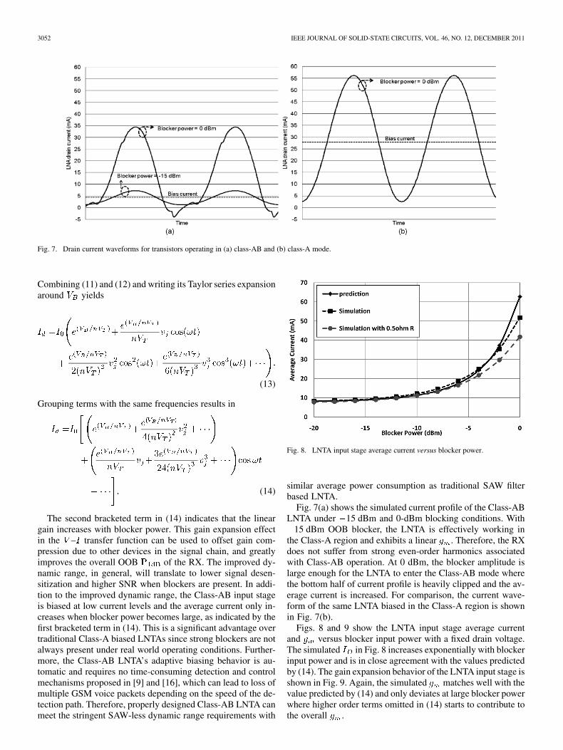
Fig. 7. Drain current waveforms for transistors operating in (a) class-AB and (b) class-A mode.
Combining (11) and (12) and writing its Taylor series expansionaround yields
(13)
Grouping terms with the same frequencies results in
(14)
The second bracketed term in (14) indicates that the lineargain increases with blocker power. This gain expansion effectin the – transfer function can be used to offset gain com-pression due to other devices in the signal chain, and greatlyimproves the overall OOB of the RX. The improved dy-namic range, in general, will translate to lower signal desen-sitization and higher SNR when blockers are present. In addi-tion to the improved dynamic range, the Class-AB input stageis biased at low current levels and the average current only in-creases when blocker power becomes large, as indicated by thefirst bracketed term in (14). This is a significant advantage overtraditional Class-A biased LNTAs since strong blockers are notalways present under real world operating conditions. Further-more, the Class-AB LNTA’s adaptive biasing behavior is au-tomatic and requires no time-consuming detection and controlmechanisms proposed in [9] and [16], which can lead to loss ofmultiple GSM voice packets depending on the speed of the de-tection path. Therefore, properly designed Class-AB LNTA canmeet the stringent SAW-less dynamic range requirements with
Fig. 8. LNTA input stage average current versus blocker power.
similar average power consumption as traditional SAW filterbased LNTA.
Fig. 7(a) shows the simulated current profile of the Class-ABLNTA under 15 dBm and 0-dBm blocking conditions. With
15 dBm OOB blocker, the LNTA is effectively working inthe Class-A region and exhibits a linear . Therefore, the RXdoes not suffer from strong even-order harmonics associatedwith Class-AB operation. At 0 dBm, the blocker amplitude islarge enough for the LNTA to enter the Class-AB mode wherethe bottom half of current profile is heavily clipped and the av-erage current is increased. For comparison, the current wave-form of the same LNTA biased in the Class-A region is shownin Fig. 7(b).
Figs. 8 and 9 show the LNTA input stage average currentand versus blocker input power with a fixed drain voltage.The simulated in Fig. 8 increases exponentially with blockerinput power and is in close agreement with the values predictedby (14). The gain expansion behavior of the LNTA input stage isshown in Fig. 9. Again, the simulated matches well with thevalue predicted by (14) and only deviates at large blocker powerwhere higher order terms omitted in (14) starts to contribute tothe overall .

YU et al.: A SAW-LESS GSM/GPRS/EDGE RECEIVER EMBEDDED IN 65-NM SOC 3053
Fig. 9. LNTA input stage �� versus blocker power.
Furthermore, Fig. 9 shows that the desirable gain expan-sion behavior of the Class-AB input stage can be reduced byDC feedback from unwanted parasitic resistance between thesource node of the input transistors and ground. Even with arelatively small source-to-ground resistance of 0.5 , simulated
at 0-dBm input power level is lower by approximately 20%.This undesirable feedback is due to the increasing averagecurrent dropping across the parasitic resistor and raising thesource voltage, which then compresses both the and ofthe input – stage. Therefore, care must be taken in the layoutto minimize parasitic resistance in the common source node ofthe input differential pair.
B. Blocker Detection
Similar to the LNTA, the idea of adaptively changing the cir-cuit performance with blocker level can be used to save power inthe LO chain. Hence, the use of blocker detection for LO powerreduction.
Like all conventional RXs, blocker signals in a SAW-less RXare down-converted to baseband by LO PN through reciprocalmixing and degrade the SNR. With OOB blocker at 0 dBm, PNrequirement is 166 dBc/Hz @ 20-MHz offset for the divider.Furthermore, in order to allow the blocker AC current from theLNTA to pass through the mixer switches without distortion,a large transistor size is chosen. Due to the stringent PN re-quirement and large switch capacitive loading, large current isconsumed in the LO buffers. Understanding that large mixerswitch size is only necessary when strong blockers are present,a blocker detector is used to determine the PN and switch sizerequirements depending on the real-time blocker profile.
Fig. 10 shows the block diagram of the blocker detector andits control mechanism. The first part of the blocker detector is apre-amplifier which is a replica of the Class-AB input stage em-bedded in the LNTA. Triggered by large blockers, the pre-am-plifier produces a detectable DC current that is compared witha fixed reference current and transformed into a control voltagethrough a simple latch circuit. It is important to note that thedetector’s Class-AB behavior does not need to match the LNAinput devices’, and the Class-AB induced current changes canbe detected within micro seconds in the event of a blocker.
Fig. 10. Block diagram of the blocker detection technique.
As shown in Fig. 10, to save the average power consumption,both frequency divider and mixer are divided into two equalparts, Mixer1/2 and Divider1/2 respectively. Mixer1 and Di-vider1 are always turned on while Mixer2 and Divider2 are con-trolled by the EN output of the blocker detector. When there isno blocker signal detected, EN is low and Mixer2 and Divider2are turned off to save power. Conversely, when a large blocker isdetected, EN becomes high and Mixer2 and Divider2 are turnedon to increase the RX dynamic range. Since the occurrence ofsuch large blocker is rare under real-life conditions, almost 50%of the divider power consumption can be saved by this blockerdetection scheme.
V. CIRCUIT IMPLEMENTATION
A. LNTA
Fig. 11 shows the differential inductive-degenerated LNTA.To attain a low-power and high-dynamic-range input – stage,the input transistors and are biased in the weak inver-sion region, as described in Section IV. The LNA is biased at8 mA and achieves a simulated NF of 1.4 dB and OOBof 1 dBm. The LNA performance is superior when com-pared with traditional Class-A amplifier designs that requires
40 mA of DC bias current for a specified of 120 mA/Vand a blocking signal at 0 dBm.
The thick-oxide cascode transistors are biased at 2.3 V toleave sufficient headroom to accommodate for blocker swingsin the intermediate nodes of the LNTA. At the LNTA output,the 2.5-V supply together with low OOB impedance providedby the highly selective frequency conversion interface, avoidsclipping and suppresses output distortion. Finally, a smallsource-degeneration inductor was used to maintain a reason-able matching while sustaining the Class-AB behavior. Thesimulated matching gain is around 12 dB.
B. Blocker Detector
Fig. 12(a) shows the schematic of the blocker detector.and are the smallest unit of the input transistors in theLNTA, i.e., and in Fig. 11. The gates of and ,
, and , are connected to nodes A and B in Fig. 11 tosense the input blocker signal. The size of in Fig. 12(a)

3054 IEEE JOURNAL OF SOLID-STATE CIRCUITS, VOL. 46, NO. 12, DECEMBER 2011
Fig. 11. LNTA schematic.
is two times and its gate is connected to nodeC in Fig. 11. and are enable switches controlled by“EN_DET” to turn on or turn off the blocker detector. and
are the resistive loads and the ratio between andis 2/3. and are used to filter the high frequency partsof and which are sensed by the latch. The latch functionis enabled when “EN_LAT” is high, and is reset when it is low.
As described in the previous subsection, to are bi-ased in the same weak inversion region as and in Fig. 11.The DC current of , , is fixed and the summation DC cur-rent of and , , increases with the increase in the re-ceived blocker signal due to the Class-AB characteristic. Whenthere is no blocker signal, is equal to , so due tothe imbalanced resistive loads. In this situation, the “EN” outputof the latch is low; Divider2 and Mixer2 in Fig. 10 are turnedoff. However, when the received blocker signal is higher thanthe 12 dBm threshold level in this design, is increased suchthat . This enables both Divider2 and Mixer2 are turnedon to handle the blocker signal.
Fig. 12(b) shows the timing diagram of the blocker detectionscheme. to are turned on by “EN_DET” 15 s prior tothe beginning of each GSM RX burst. After 5 s for the settlingof and , the latch function is enabled by “EN_LAT”. Thereare 10 s for divider and mixer to settle before the RX burst inthis design. As shown in Fig. 12(b), at the end of the RX burst,the blocker detector is reset and the cycle repeats in the next RXburst.
C. Output Load of LNTA and Frequency-Conversion Interface
The LNA load inductor shown in Fig. 4 is implementedby the top two layers of thicker metals for higher factor. Fur-thermore, to save area and increase the inductance, the stackstructure is used. As described in Section III, to suppress theoutput voltage swing at the LNTA output node, the resonantfrequency of is located at approximately 1/4 of the
Fig. 12. (a) Blocker detector schematic. (b) Timing diagram of the blocker de-tection scheme.
Fig. 13. LB simulation results of the mixer and LPF output blocker currentversus the input blocker power at 20 MHz offset.
LO frequency, which are 230 and 510 MHz in LB and HB, re-spectively. In this design, with 0-dBm 20-MHz offset blockerin the LB case, the LNA single-ended output voltage swing is
400 mV, which is still far from the voltage swing limitationof 800 mV.
For the direct conversion receiver (DCR), the basebandGSM signal is located from DC to 100 kHz while the closest0-dBm blocker is located at 20 MHz. Therefore, in this design,the pole of the LPF is set to 2 MHz which provides at least20-dB rejection for the down-converted blocker current beforeentering TIA, while preserving the in-band signal. As described

YU et al.: A SAW-LESS GSM/GPRS/EDGE RECEIVER EMBEDDED IN 65-NM SOC 3055
Fig. 14. Block diagram of the 25% clock generator.
Fig. 15. Schematic of the opamp.
in Section III, in Fig. 3(b) should be designed as largeas possible to suppress the blocker voltage swing at the mixerinput and output ports. However, in practice, its size is limitedby the available chip area. In this design, to maximize thecapacitance density, MOM capacitors are stacked on top of theaccumulation-mode MOS varactors for the implementa-tion. Fig. 13 shows the LB simulation results of the mixer andLPF output blocker current versus the input blocker power at20-MHz offset. It is shown that the mixer is still linear whenthe blocker power is 2 dBm, and the slight current expansionis from the Class-AB LNTA. Furthermore, the blocker currentafter LPF is only 1.15 mA when the blocker power is 0 dBm,which is a reasonable input current for TIA under normaloperation.
D. 25% Clock Generator
The fully integrated fractional- frequency synthesizeroperates at twice the LO frequency and a divide-by-2 anddivide-by-4 circuits are used to generate 25% duty-cycle IQ LOsignals in HB and LB, respectively. The block diagrams of bothclock generators are shown in Fig. 14. Each divider implementsa divide-by-2 function and consists of two cross-connectedD-flip-flops which are formed by clocked inverters in orderto obtain large signal swing [17]. In HB, the outputs of thedivider circuit have 50% duty cycle and they are applied to theNOR gates to generate the required 25% duty-cycle IQ signals.In LB, the outputs of the second divider are re-timed by the
Fig. 16. Block diagram of the VCO, including dual path varactors and switchedcapacitor array (SCA).
Fig. 17. Die micrograph.
outputs of the first divider to generate the 25% duty-cycle IQsignals. Therefore, the noise from the second divider does notcontribute to the final IQ signals. The re-timed circuit in Fig. 14is implemented by AND gates.
E. TIA
The TIA stage is a fully differential operational amplifierconnected with feedback resistors and capacitors as shown inFig. 3(b). The resistor value is determined by the conversiongain and the RC low-pass corner is determined by the RX fil-tering requirement.
3056 IEEE JOURNAL OF SOLID-STATE CIRCUITS, VOL. 46, NO. 12, DECEMBER 2011
Fig. 18. Balun and matching network.
Fig. 19. RX gain and sensitivity.
The schematic of the op-amp is shown in Fig. 15. Class-ABoutput stage is used to maximize the dynamic range. The opampis designed with low noise in order to avoid the noise amplifica-tion factor increasing the opamp noise contribution to the wholeRX [18]. Large input transistor sizes are chosen to achieve lowflicker noise and degeneration resistors are also used to suppressthe noise from the nMOS load in the first stage. Special caremust be taken to ensure circuit stability due to the large secondpole introduced by the large capacitance from the current-modeLPF.
F. Frequency Synthesizer
To achieve excellent OOB blocker performance, the designchallenges of the frequency synthesizer are to achieve low ref-erence spur and good PN at 20 MHz away from carrier. Con-sider the case for a 0-dBm LB blocker at 20 MHz away fromcarrier, VCO PN is required to be 154 dBc/Hz around 4 GHzin order to maintain sufficient SNR at baseband. In this work, adual-path loop filter [19] is adopted to save chip area.
1) Spur Control: To prevent low-frequency harmonics cou-pling to the VCO frequency, first- or second-order passive RC
Fig. 20. RX GSM BER and EDGE EVM versus blocker power, where GSMsignal power is �99 dBm and EDGE signal power is �85 dBm.
filters are applied between the LDOs and circuits of the syn-thesizer which can provide sufficient rejection. The locations ofall capacitors and resistors are carefully placed for better iso-lation. The ground planes of the synthesizer are separated intohigh frequency and low frequency parts. Sensitive circuits suchas VCO and bandgap circuit use the high-frequency ground;while others use the low-frequency ground. The metal shieldingis often used to isolate sensitive nodes from active signal lines.The charge-pump linearity is improved by using smaller switchsizes and symmetric layout.
2) VCO: The VCO core circuit is shown in Fig. 16. ThenMOS-only architecture is selected because it offers highervoltage headroom under a given supply voltage. Moreover, fora specified negative resistance, the nMOS cross-coupled pairis much smaller than the pMOS one; hence the nMOS-onlyarchitecture also minimizes the nonlinear junction capacitanceand reduces supply pushing. In this design, a tail resistor,R1 in Fig. 16, is used to bias the VCO to avoid flicker noiseup-conversion. The VCO is supplied by a voltage of 2.45 Vfrom LDO and R1 is implemented by a programmable resistorto set the bias current. The switched capacitor array followsa conventional design [20] and all MOS devices have thickoxides to avoid reliability issues.
The inductor is one of the most important passive componentsin the VCO because it accounts for 70% of the total LC-tankloss. Moreover, it is vulnerable to magnetic coupling which mayresult in symmetric spurs due to the limiter transfer action. Inthis work, field-cancelling inductors [21] are used in order toprovide rejection from the common-mode magnetic field. Sinceit behaves as a dipole, it also prevents coupling into other res-onators in the SoC. The aspect ratio of the inductor is sized insuch a way to achieve best available , considering mutual in-ductance and metal loss tradeoff. In the 65-nm process tech-nology, the AL-RDL layer alone is used for inductor routing

YU et al.: A SAW-LESS GSM/GPRS/EDGE RECEIVER EMBEDDED IN 65-NM SOC 3057
Fig. 21. RX DC current versus blocker power.
Fig. 22. Measured IIP3.
due to its lower sheet resistance. Simulated inductance is 1 nH,and is around 22 at 4 GHz.
VI. MEASUREMENT RESULTS
Fig. 17 shows the die micrograph of the transceiver portion inthe 65 nm CMOS SoC chip. The chip is packaged in a 179-ballFCCSP package and the total chip size is 8.6 8.1 mm wherethe transceiver occupies a die area of 2.6 1.9 mm . Operatingunder a 3.8-V external supply, the RX and synthesizer draw 37.1and 21.8 mA, respectively, in the continuous RX mode. The RXcurrent increases to 60 mA when a 0-dBm OOB blocker ispresent.
To demonstrate true SAW-less operation, all measurementsare performed on PCB with L-C lattice-type balun and matchingnetwork, as shown in Fig. 18. The inductance and capacitanceare 12/3.3 nH and 2.2/1.5 pF in LB/HB, and the simulated max-imum amplitude and phase imbalance in LB/HB are 1.1/1.7 dBand 1 /0.9 , respectively. When no blockers are present, the
Fig. 23. Measured IIP2.
Fig. 24. Synthesizer phase noise profile.
measured RX gain and sensitivity for all channels are shownin Fig. 19. The typical gain is 60 dB, while the sensitivityis 110 dBm, which is comparable to the conventional RXwith SAW filters. The measured OOB is 1 dBm andthe RX’s robustness to blocker interference is demonstrated inFig. 20, where the BER remains for blocker powersof 4.3/4.7 dBm at 20/80-MHz offset for the GSM850/DCS

3058 IEEE JOURNAL OF SOLID-STATE CIRCUITS, VOL. 46, NO. 12, DECEMBER 2011
TABLE IRX PERFORMANCE SUMMARY
band. Similarly, the RX EVM remains for blockerpower 2 dBm when operating under MCS-9 in EDGE mode.
The blocker detection function is implemented in HB onlysince the HB divider consumes more power due to higher opera-tion frequency. Fig. 21 plots the measured RX current versus the80-MHz offset blocker power in HB. Notably, the Mixer2 andDivider2 in Fig. 10 also can be manually controlled in this de-sign. It can be observed that the blocker detector turns on Mixer2and Divider2 when the blocker level is larger than 13 dBm,which is 1 dB less than the prediction. The discrepancy fromsimulation mainly comes from the device mismatch since thesmallest unit of the LNA input transistor is used for blockerdetection. Therefore, one should keep enough margins to tol-erate such device mismatch. As shown in Fig. 21, 4 mA can besaved when the blocker level is smaller than 13 dBm. Whenthe blocker detection function is turned on, an additional 1 dBof blocker margin is achieved.
The IIP3 is measured with two tones located on 0.8- and1.6-MHz offset frequencies. Fig. 22 plots the measured IIP3 atthe maximum gain for all channels from GSM850 to PCS. TheIIP3 is around 0 dBm which is much better than the voltage-mode RX since the stage between the LNA and mixer hasbeen removed.
The IIP2 is measured with two tones located at 6- and6.1-MHz offset frequencies. Over 1300 chips cross five dif-ferent process corners are measured. Fig. 23 plots the measuredIIP2 distribution at the center channel in GSM850 and DCS.The worst IIP2 is around 50 dBm, which is 20 dB above thedesign requirement. Since the LPF corner in this design is
2 MHz, the two-tone voltage swing at the input and output ofthe mixer is suppressed, resulting in better IIP2 performance.
Without the SAW filters, the measured LB RX andrejections are 68 and 44 dB, respectively. A blocker
around the harmonics can be down-converted to aroundthe signal band, causing RX SNR degradation. Moreover, theclose-in LO PN within the corresponding offset frequency rangeis also down-converted to the signal band and degrades the RXSNR further. When the BER is , exceptions must betaken as the desired signal cannot be decoded properly. The RXrequires 4/4/6/8 exceptions in the GSM850/GSM900/DCS/PCSband, which satisfy the ETSI limit of 24 exceptions per band.
The measured PN profile of the 3.536-GHz synthesizer outputsignal is shown in Fig. 24. The PN is 83.9, 92.6, 116.8,
138.5, and 149.3 dBc/Hz at 10-k, 100-k, 400-k, 3-M, and10-MHz offset, respectively. Finally, the synthesizer exhibits
85-dBc reference spur at 26-MHz offset. Aided by inter-ference cancellation techniques [22] implemented in the dig-ital baseband core, the reference spur results in negligible SNRdegradation with blockers applied at frequencies equal to mul-tiples of the 26-MHz reference.
The RF transceiver performance results are summarized inTable I. Although [9] does not require any external components,this work has 1.4 dB better NF in the 20-MHz blocker casewhen the blocker power is 11 dB larger than that in [9]. In addi-tion, this work provides more than 6-dB NF margin in the 20/80blocker case, which translates to greater tolerances for PCB andexternal component variations.

YU et al.: A SAW-LESS GSM/GPRS/EDGE RECEIVER EMBEDDED IN 65-NM SOC 3059
VII. CONCLUSION
This paper demonstrates the possibility of replacing thediscrete SAW filter function with inexpensive on-chip com-ponents to reduce cost and form factor for today’s cellularsystem. This is achieved by employing several techniques,including current-mode RX with highly selective frequencyconversion interface, Class-AB self-bias LNTA, and blockerdetection. In addition, careful RX system budgeting to allowmaximum usage of voltage and linearity headroom for everystage translates to a fully optimized solution. The measurementresults show that the overall performance, current consumption,and die area all meet or exceed that of a typical SAW-basedRX. Furthermore, the device has passed the full type approval(FTA) test with margins and reached a mass-production state.
REFERENCES
[1] [Online]. Available: http://en.wikipedia.org/wiki/GSM[2] H. Darabi et al., “A quad-band GSM/GPRS/EDGE SoC in 65 nm
CMOS,” IEEE J. Solid-State Circuits, vol. 46, no. 4, pp. 870–882,Apr. 2011.
[3] C. H. Wang et al., “A direct digital frequency modulation PLL with alldigital on-line self-calibration for quad-band GSM/GPRS transmitter,”in Proc. IEEE Symp. VLSI Circuits, 2009, pp. 190–191.
[4] B. Bakkaloglu, P. Fontaine, A. N. Mohieldin, S. Peng, and F. Dulger,“A 1.5-V multi-mode quad-band RF RX for GSM/EDGE/CDMA2Kin 90-nm digital CMOS process,” IEEE J. Solid-State Circuits, vol. 41,no. 5, pp. 1149–1159, May 2006.
[5] J. Ryynanen, K. Kivekas, J. Jussila, L. Sumanen, A. Parssinen, andK. A. I. Halonen, “A single-chip multimode receiver for GSM900,DCS1800, PCS1900, and WCDMA,” IEEE J. Solid-State Circuits, vol.38, no. 4, pp. 594–602, Apr. 2003.
[6] P. Sivonen, J. Tervaluoto, N. Mikkola, and A. Parssinen, “A 1.2-V RFfront-end with on-chip VCO for PCS1900 direct conversion receiverin 0.13-�m CMOS,” IEEE J. Solid-State Circuits, vol. 41, no. 2, pp.384–394, Feb. 2006.
[7] D. Kaczman, M. Shah, M. Alam, M. Rachedine, D. Cashen, L. Han,and A. Raghavan, “A single-chip 10-band WCDMA/HSDPA 4-bandGSM/EDGE SAW-less CMOS receiver with digRF 3G interfaceand �90 dBm IIP2,” IEEE J. Solid-State Circuits, vol. 44, no. 3, pp.718–739, Mar. 2009.
[8] N. Kim, L. E. Larson, and V. Aparin, “A highly linear SAW-less CMOSreceiver using a mixer with embedded Tx filtering for CDMA,” IEEEJ. Solid-State Circuits, vol. 44, no. 8, pp. 2126–2137, Aug. 2009.
[9] A. Mirzaei, H. Darabi, A. Yazdi, Z. Zhou, E. Chang, and P.Suri, “A 65 nm CMOS quad-band SAW-less receiver SoC forGSM/GPRS/EDGE,” IEEE J. Solid-State Circuits, vol. 46, no. 4, pp.1–15, Apr. 2011.
[10] A. Mirzaei et al., “Analysis and optimization of current-driven passivemixers in narrowband direct-conversion receivers,” IEEE J. Solid-StateCircuits, vol. 44, no. 10, pp. 2678–2688, Oct. 2009.
[11] X. Fan, H. Zhang, and E. Sinencio, “A noise reduction and linearityimprovement technique for a differential cascode LNA,” IEEE J. Solid-State Circuits, vol. 43, no. 3, pp. 588–599, Mar. 2008.
[12] T. H. Lee, The Design of CMOS Radio-Frequency Integrated Circuits,2nd ed. Cambridge, U.K.: Cambridge Univ. Press, 2004.
[13] P. R. Gray and R. G. Meyer, Analysis and Design of Analog IntegratedCircuits, 4th ed. New York: Wiley, 2001.
[14] K. L. Fong, C. D. Hull, and R. G. Meyer, “A class AB monolithic mixerfor 900-MHz applications,” IEEE J. Solid-State Circuits, vol. 32, no.8, pp. 1166–1171, Aug. 1997.
[15] Y. Tsividis, Operation and Modeling of the MOS Transistor, 2nd ed.Boston, MA: McGraw-Hill, 1999.
[16] W. Xiong and L. E. Larson, “An �-band low-noise amplifier with self-adjusting bias for improved power consumption and dynamic range ina mobile environment,” in IEEE MTT-S Int. Microw. Symp. Dig., Jun.1999, pp. 497–500.
[17] M. D. Tsai, “Low-Noise Frequency Divider,” U.S. Patent 7 719 327,May 18, 2010.
[18] M. Valla, G. Montagna, R. Castello, R. Tonietto, and I. Bietti, “A72-mW CMOS 802.11a direct conversion front-end with 3.5 dB NFand 200-kHz ��� noise corner,” IEEE J. Solid-State Circuits, vol. 40,no. 4, pp. 970–977, Apr. 2005.
[19] D. Mijuskovic, M. Bayer, T. Chomicz, N. Garg, F. James, P. McEn-tarfer, and J. Porter, “Cell-based fully integrated CMOS frequency syn-thesizer,” IEEE J. Solid-State Circuits, vol. 29, no. 3, pp. 271–271, Mar.1994.
[20] P. Andreani, K. Kozmin, P. Sandrup, M. Nilsson, and T. Mattsson, “ATX VCO for WCDMA/EDGE in 90 nm RF CMOS,” IEEE J. Solid-State Circuits, vol. 46, no. 7, pp. 1618–1618, Jul. 2011.
[21] A. Poon, A. Chang, H. Samavati, and S. S. Wong, “Reduction of in-ductive crosstalk using quadrupole inductors,” IEEE J. Solid-State Cir-cuits, vol. 44, no. 6, pp. 1756–1756, Jun. 2009.
[22] J. G. Andrews, “Interference cancellation for cellular systems: Acontemporary overview,” IEEE Wireless Commun., vol. 12, no. 2, pp.19–29, Apr. 2005.
Chi-Yao Yu (M’10) was born in Taipei, Taiwan, in1978. He received the M.S. degree in communica-tion engineering from National Tsing Hua Univer-sity, Hsinchu, Taiwan, in 2002, and the Ph.D. degreein electronics engineering from National Chiao TungUniversity, Hsinchu, Taiwan, in 2008.
He has been with MediaTek Inc., Hsinchu, Taiwan,since 2008, where he is working on analog and RFIC design for wireless communications. His currentresearch interest is ultrahigh dynamic range receiversfor cellular systems.
Ivan Siuchuang Lu (M’04) was born in Taipei,Taiwan, in 1979. He received the B.E.E. degree fromthe University of Queensland, Brisbane, Australia,in 2001, and the Ph.D. degree from the University ofNew South Wales, Sydney, Australia, in 2006.
After graduation, he joined Marvell Semicon-ductor, Santa Clara, CA, where he contributedto transceiver design for MIMO WiFi and GPSapplications. He has been with Mediatek USA, SanJose, CA, since 2009 and is currently a Memberof Technical Staff. His current research interests
include advanced RF CMOS transceiver architectures and circuits for wirelesscommunication systems.
Yen-Horng Chen was born in Taipei, Taiwan, in1977. He received the B.S. and M.S. degrees in elec-trical engineering from National Taiwan University,Taipei, Taiwan, in 1999 and 2001, respectively.
From 2001 to 2005, he was with IndustrialTechnology Research Institute (ITRI) and workedon IF PGAs, filters, and AGC design for WCDMA,DAB, and UWB standards. In 2005, he joinedMediatek, Hsinchu, Taiwan, as a Technical Manager,where he developed low-noise receiver front-ends inCMOS process, digital auto-calibration for receiver
impairment, receiver system planning, and analysis for GSM/EDGE standard.In 2010, he joined Mediatek, Austin, TX, where he is developing all-digitalPLL and LTE transceivers.
Lan-Chou Cho was born in Taipei, Taiwan, in1978. He received the B.S., M.S., and Ph.D. degreesin electrical engineering from National TaiwanUniversity, Taipei, Taiwan, in 2001, 2003, and 2008,respectively.
He is currently with Mediatek Inc., Hsinchu,Taiwan. His research interests include phase-lockedloops, delay-locked loops, and high-speed CMOSdata-communication circuits for multiple gigabitapplications.

3060 IEEE JOURNAL OF SOLID-STATE CIRCUITS, VOL. 46, NO. 12, DECEMBER 2011
Chih-Hao Eric Sun was born in Taipei, Taiwan, in1978. He received the B.S. and M.S. degrees in elec-trical engineering from National Taiwan University,Taipei, Taiwan, in 2000, and 2002, respectively.
He is currently with Mediatek Inc., Hsinchu,Taiwan, working on cellular products.
Chih-Chun Tang was born in Taipei, Taiwan, in1974. He received the Ph.D. degree from the Grad-uate Institute of Electronics Engineering, NationalTaiwan University, Taipei, Taiwan, in 2002.
He has been with the RF Department, MediaTekInc., Hsinchu, Taiwan, since 2002 and joined the de-sign of GSM/EDGE RF stand-alone transceivers andSOCs. Now, he is the RF Transceiver Project Leaderof 3G WCDMA.
Hsiang-Hui Chang received the B.S., M.S., andPh.D. degrees in electrical engineering from Na-tional Taiwan University, Taipei, Taiwan, in 1999,2001, and 2004, respectively.
He is currently with MediaTek Inc., Hsinchu,Taiwan, where he is involved with wireless com-munication products. His research interests aredigital-enhanced PLLs, all-digital frequency syn-thesizers, RF system architecture design, anddigital-assisted transceiver design.
Wen-Chang Lee (M’10) received the B.S. degree inelectrical engineering from the National Sun-Yat-SenUniversity, Kao-Hsiung, Taiwan, in 2000, and theM.S. degree in communication engineering from theNational Chiao Tung University, Hsin-Chu, Taiwan,in 2002.
From 2002 to 2008, he was with VIA Technolo-gies, Inc., Taipei, Taiwan, working on cellular andwireless-LAN RF transceivers, as a Design Lead inthe GSM/GPRS/EDGE synthesizer and transmitterdevelopment. In 2008, he joined MediaTek, Hsinchu,
Taiwan, focused on VCO and synthesizer in cellular applications. Since 2010,he has been with the MediaTek, Austin, TX, as a Technical Manager workingon advanced synthesizer architecture.
Sheng-Jui Huang was born in Kaohsiung, Taiwan, in1974. He received the M.S.E.E degree from NationalChiao Tung University, Hsinchu, Taiwan.
From 2000 to 2005, he was with Realtek Semi-conductor, where he was involved with mixed-signalcircuits and line drivers for Gigabit Ethernet. In2005, he joined MediaTek, Hsinchu, Taiwan, as aTechnical Manager, where he developed high-def-inition audio ADC and continuous-time delta-sigmaADC for telecommunications. He currently workson synthesizer-related circuitry.
Tzung-Han Wu (S’06–M’07) was born in Taipei,Taiwan, in 1979. He received the B.S. and M.S. de-grees from the Department of Electrical Engineering,National Chung-Hsing University, Taichung, Taiwan,in 2001 and 2003, respectively, and the Ph.D. degreein communication engineering from National Chiao-Tung University, Hsinchu, Taiwan, in 2007.
He worked on receiver circuits using CMOS, SiGeHBT and GaInP/GaAs HBT technologies. Currently,he is with the RFIC Design Department, MediaTekInc., Hsinchu, Taiwan. His current research interests
are in the areas of RF receivers and multi-radio SOC. He designs receiver front-ends and is the top integrator in 2G and 3G SoC products.
Dr. Wu is a member of Phi Tau Phi.
Chinq-Shiun Chiu was born in Taiwan in 1971. Hereceived the B.S. degree from National Tsing HuaUniversity, Hsinchu, Taiwan, in 1993, and the M.S.degree from National Taiwan University, Taipei,Taiwan, in 1995, both in electrical engineering.
He is currently a design manager with MediaTekInc., Taiwan. His interests include analog and RF ICdesign for cellular transceiver and multi-radio systemintegration in SOC. He holds over 10 issued patentswith Mediatek Inc.
George Chien (M’00–SM’10) was born in Athens,GA, in 1971. He received the B.S. degree from theUniversity of California, Los Angeles, in 1993, andthe M.S. and Ph.D. degrees from the University ofCalifornia, Berkeley, in 1996 and 1999 respectively,all in electrical engineering and computer science.
In January 2000, he joined Marvell Semicon-ductor, Santa Clara, CA, where he worked on severalgenerations of transceivers for WLAN and BT. InJanuary 2008, he joined MediaTek, Inc., where hefocuses on a wide range of transceivers designs from
cellular to connectivity applications in SOC applications. He is currently aDirector of RF design division with MediaTek, Inc., San Jose, CA. He holdsover 15 issued and several pending patents and has published over ten IEEEconference and journal papers. His research interests include novel transceiverarchitecture and circuit designs for deep-submicron CMOS processes.
Dr. Chien was a corecipient of ISSCC Jack Kilby Award for OutstandingStudent Paper in 1997. Since 2006, he has been serving on the ISSCC TechnicalProgram Committee.