Embed Size (px)
Citation preview

IEEE JOURNAL OF SOLID-STATE CIRCUITS, VOL. 43, NO. 12, DECEMBER 2008 2853
Equalization of Third-Order IntermodulationProducts in Wideband Direct Conversion Receivers
Edward A. Keehr, Student Member, IEEE, and Ali Hajimiri, Member, IEEE
Abstract—This paper reports a SAW-less direct-conversionreceiver which utilizes a mixed-signal feedforward path to regen-erate and adaptively cancel IM3 products, thus accomplishingsystem-level linearization. The receiver system performance isdominated by a custom integrated RF front end implemented in130-nm CMOS and achieves an uncorrected out-of-band IIP3 of
7.1 dBm under the worst-case UMTS FDD Region 1 blockingspecifications. Under IM3 equalization, the receiver achieves aneffective IIP3 of �5.3 dBm and meets the UMTS BER sensitivityrequirement with 3.7 dB of margin.
Index Terms—Adaptive equalization, adaptive signal processing,digital linearization, feedforward equalization, mixed-signal lin-earization, nonlinear circuits, postdistortion, RF receivers, system-level linearization, wireless communications.
I. INTRODUCTION
S ELF-GENERATED interference in RF receivers is the gen-eral result of signals interacting with circuit block nonide-
alities in such a way that error terms arise and corrupt the desiredsignal intended for reception. This interference is sometimes sosevere that even increasing the circuit area and power dissipationarbitrarily to reduce the nonidealities is insufficient, and costlyoff-chip components are required for the receiver to meet spec-ification. Often, this self-generated interference manifests itselfas distortion products due to circuit block nonlinearities, but canalso arise due to I-Q mismatch, interstage coupling, or variousother mechanisms.
Unfortunately, it can also be said that these problems worsenin general as CMOS processes continue to scale. As supply volt-ages drop, less headroom is available to apply large overdrivebias voltages to devices, worsening their linearity and matchingproperties. Furthermore, as market pressures demand the furtherreduction in the number and size of off-chip components, auxil-iary blocks that once facilitated receiver design, such as off-chipSAW filters, will become extinct. Therefore, there exists a greatneed to conceive and develop monolithic solutions to self-gen-erated interference problems in RF receivers.
II. SYSTEM-LEVEL SOLUTIONS
A. General Solution Strategies
Although the prognosis for self-generated interference issuesis bleak, the nature of the problem yields a plausible solution
Manuscript received April 07, 2008; revised August 06, 2008. Current versionpublished December 10, 2008. This work was supported in part by an NDSEGFellowship and by the Lee Center for Advanced Networking.
The authors are with the California Institute of Technology, Pasadena, CA91125 USA (e-mail: [email protected]).
Digital Object Identifier 10.1109/JSSC.2008.2005701
Fig. 1. General adaptive feedforward receiver concept.
strategy. Most significantly, the error-producing signal is re-tained in the system at some point, while the error-generationmechanism is known, at least qualitatively. This knowledge wasdelineated in a general scheme described in [1] in which errorproducers within the RF receiver were applied to a rough modelof the error generation mechanism to generate a reference signalconsisting of solely the corruptive error. However, the actualmodel of the error is never known precisely. Hence, as shown inFig. 1, an adaptive equalization algorithm is employed to sub-tract the reference signal from the corrupted main receiver path,as it can account for minor uncertainties in the effective alter-nate path baseband transfer function. Note that for simplicity inFig. 1, only a dc gain uncertainty is shown.
Such a system-level solution methodology is advantageousfor many reasons, not the least of which is its indifferencetowards the details of the original receiver. As this techniquefocuses only on cancellation of the error itself and not the errorproducers, it permits a relatively narrowband alternate path.That is, although large, undesired, error-producing signals mayoccur over a wide frequency range, the relevant error terms thatthey produce are only restricted to a much smaller bandwidthequal to that of the desired signal. The circuits processing theerror operate with a lower dynamic range than their originalreceiver counterparts, as the corruptive error to noise ratio is ingeneral much less than the error producer to noise ratio in the
0018-9200/$25.00 © 2008 IEEE
Authorized licensed use limited to: CALIFORNIA INSTITUTE OF TECHNOLOGY. Downloaded on March 31, 2009 at 12:57 from IEEE Xplore. Restrictions apply.

2854 IEEE JOURNAL OF SOLID-STATE CIRCUITS, VOL. 43, NO. 12, DECEMBER 2008
TABLE IREPORTED IIP3 SPECIFICATION AND PERFORMANCE COMPARISON
1) Measurement at mixer transconductor input
main path. Also, if the LMS algorithm is used to perform theadaptive equalization, multiple LMS loops in parallel can beused to cancel different interference signals as shown in Fig. 1.[2] Finally, in the event that the self-generated interference ofinterest is due to large, undesired blocker signals, the powerdissipation of an alternate path can be further reduced by onlypowering it on when needed, as most receivers only need tooperate in the presence of strong interferers for a small fractionof the time.
B. Study Motivation and Application to Nonlinear RFReceivers
Due to the continued and rising popularity of FDD standardsfor 3G wireless communications, of notable current interest tothe circuit design community is the task of improving the lin-earity of RF receiver front ends. It has been recognized in recentreports that adaptive feedforward error cancellation is useful indealing with this problem [2]–[4]; however, the current literatureonly contains at most descriptions of high-level system studiesimplemented with discrete RF components. Hence, it is desir-able to study the implications of applying this technique to aspecification-compliant custom-designed RF front end to assessits suitability for commercial devices. This paper describes anexperiment in which such a front end is implemented for theUMTS Region 1 standard in order to compensate for the ex-acting linearity requirements implicitly imposed by the FDDout-of-band blocker test [5]. In order to meet these require-ments, several reported commercial receivers [6]–[8] have re-sorted to the use of interstage SAW filters to attenuate largeblocker signals and hence to relax requirements on the inte-grated circuit blocks. Recently, several SAW-less UMTS re-ceivers have also been reported, albeit with somewhat lower outof band IIP3 performance [9]–[11]. It should be noted that re-ported IIP3 specifications and achievements vary widely withinthe literature, as shown in Table I. This variation is, at leastin part, due to the fact that the IIP3 specification depends onthe receiver achieved noise figure, the peak TX power whichmust be handled, and the characteristics of the particular du-plexer used, as discussed in Section III-B. Although the SAW-less receivers mentioned above meet their respective self-im-posed out-of-band IIP3 specifications, it is worthwhile to con-sider the design of SAW-less receivers with still higher IIP3 inthis context in order to permit the use of less stringent, and pos-sibly also less expensive, duplexer blocks.
The general concept behind the adaptive feedforward IM3cancellation scheme introduced in this work is shown in Fig. 2.In this figure, a nonlinear main receiver path is subject to twolarge blockers such that the desired signal is overwhelmed by the
Fig. 2. Adaptive feedforward error cancellation concept applied to RF receiverthird-order distortion in this work.
Fig. 3. FDD two-tone blocking problem.
self-generated IM3 interference products. The figure reflects thefact that the UMTS out-of-band blocking requirement [5] is animplicit two-tone test with one of the “tones” being the modu-lated TX output leakage through the antenna duplexer, as shownin Fig. 3. Reference IM3 products are generated at RF by a cubicterm generator, while choosing the LO frequency of the alternatepath mixer to be the same as that of the main path guarantees thatthe proper set of IM3 products are downconverted to basebandcharacteristics. Baseband postfiltering attenuates to negligiblelevels unwanted IM3 products in the alternate path such that theadaptive equalizer converges based only on the statistics of theIM3 products corrupting the desired signal at baseband. In thisfashion, the equalized IM3 products of the alternate path can bedirectly subtracted from the main path, leaving only the desiredRX signal. Note that this technique is not limited to a two-tonetest but also removes IM3 products resulting from a three-tonetest. Furthermore, this technique does not require prior knowl-edge of one or more of the blocker frequencies, as do techniquesthat rely on the cancellation of TX leakage to meet the UMTSlinearity specifications [12], [13]. Although both IM2 and IM3products can be concurrently cancelled by parallel LMS adap-tive filters, it was decided in this project to leverage recent work[14], [15] to perform local IIP2 improvements in order to avoidadding additional ADCs to the system to pass reference IM2products.
Most importantly, the technique described in this paperdiffers from those presented in [3] and [4] in that referenceIM3 products are generated at analog RF rather than at digitalbaseband. It can be shown with trigonometric identities thatthe resultant downconverted IM3 products are the same as
Authorized licensed use limited to: CALIFORNIA INSTITUTE OF TECHNOLOGY. Downloaded on March 31, 2009 at 12:57 from IEEE Xplore. Restrictions apply.

KEEHR AND HAJIMIRI: EQUALIZATION OF THIRD-ORDER INTERMODULATION PRODUCTS 2855
Fig. 4. Experimental UMTS receiver architecture.
those that would have been produced by I and Q basebandcubic term generators. IM3 generation in the continuous-timedomain as performed in this work is the preferred methodin an integrated downconversion receiver since it permits theuse of relatively narrowband postfilters and ADCs, such asthose based on . For the architectures in [3] and [4] tocancel IM3 products for UMTS, the ADCs must pass the fullspectrum of potential problematic blockers (1670–1850 MHz,1920–1980 MHz, 2015–2075 MHz) and would require at least6 Nyquist ADCs and digital paths with sampling rates in excessof 60 MHz. Such requirements render this strategy unattractivein that this new circuitry would consume far more power thanthe original mixed-signal and digital portion of the receiver.Given that IM3 generation is therefore to be performed in theanalog domain, it should additionally be performed at RF afterthe LNA, where the blocker magnitudes are at their largestpoint in the receiver.
III. RECEIVER ARCHITECTURE
A. Receiver Architecture Description
The receiver architecture described in this paper is shown inFig. 4. It centers around a custom-designed front end imple-mented in 130-nm RF CMOS. The chip is fully ESD protectedand operates off of a 1.2 V supply, except for the bandgapcircuitry that operates off of 2.7 V (drawing 2.5 mA). The chipis placed on a gold-plated dielectric substrate which is thenmounted onto the PCB. Analog baseband circuitry is imple-mented on the PCB using low-power commercially availablediscrete components. Finally, a digital back end containing ratechange, channel filtering, and equalization blocks is imple-mented on an FPGA platform.
Although it is possible to perform the equalization in analogcircuitry, shifting as much of the signal processing to the digitaldomain affords several advantages. For example, the behavior ofdigital circuitry is relatively insensitive to process variations, thecontinued scaling of CMOS processes has rendered basebanddigital blocks power-competitive compared to equivalent analogblocks [16], and digital circuits facilitate the implementation ofreconfigurable multimode receivers [17].
Implementing the baseband components off-chip has negli-gible impact on this experiment, as the integrated front end typ-
Fig. 5. Expected UMTS blocker profile at various points in the receiver.
ically dominates the performance of the RF receiver. In an ac-tual implementation, the receiver main path would also includeVGA functionality. The experimental receiver described hereinis for proof-of-concept only and represents the case when thereceiver is attempting to decode a signal near sensitivity. Werea VGA present in the main path, and were its gain to be changedduring alternate path operation, the adaptive nature of the alter-nate path would allow the equalizer to quickly track the changeand maintain IM3 cancellation.
B. Translation of Specification to System Requirements
In order to determine the worst-case blocking (alternativelydenoted as peak blocking) scenario seen by the receiver cir-cuitry, the UMTS blocker specification [5] must be used in con-junction with the frequency response of the duplexer shown inFig. 3. From Fig. 5 it can be seen that for the duplexer describedin [18], the largest IM3 products occur when 1.98 GHz,
2.05 GHz, and 2.12 GHz. In this case, theblocker powers are 28 dBm and 30 dBm atthe antenna and 26 dBm and 34 dBm at theLNA input. Interestingly, in this case, the worst-case blockingscenario does not occur over the band in which the specified CWblocker is 15 dBm.
According to [19], the UMTS specifications impose ananalog requirement of 9 dB at the antenna.Adopting a more general definition of NF, which will be de-noted as error figure (EF) to encompass other forms of errorincluding distortion products, the UMTS specification allows
3 dB under blocking conditions. In other words,12 dB. Given the insertion loss of the duplexer
[18] 1.8 dB and that , it iseasily computed that 7.2 dB and10.2 dB at the LNA input.
For UMTS, the noise due to the 50 source resistanceis 108 dBm 3.84 MHz at the LNA input. De-noting all quantities as LNA input-referred, this impliesthat after removing source noise, the maximum allowed re-ceiver noise power is 101.7 dBm 3.84 MHz.Assuming that the error under worst-case blocking is dom-inated by thermal noise and IM3 distortion, the error figurelimit implies that the rms sum of andis 98.2 dBm/3.84 MHz, where is the max-imum allowed IM3 distortion product power. It follows
Authorized licensed use limited to: CALIFORNIA INSTITUTE OF TECHNOLOGY. Downloaded on March 31, 2009 at 12:57 from IEEE Xplore. Restrictions apply.

2856 IEEE JOURNAL OF SOLID-STATE CIRCUITS, VOL. 43, NO. 12, DECEMBER 2008
that 100.8 dBm 3.84 MHz. Using these valuesin expression (1) yields 3.4 dBm.
(1)
The problem with this requirement is that it is inconsistentwith typical attainable values for SAW-less receivers in the ab-sence of special enhancements. For example, typical values for
range from 8 to 12 dBm [13]. For the initial de-sign in this work, the simulated values for andare 17 dB and 6 dBm, respectively. Recalling the IIP3 rela-tion (2) from [20], as used in [13], such design values yield
9.1 dBm for a mixer IIP3 of 8 dBm
(2)
Clearly a significant discrepancy arises and some sort of ad-ditional IIP3 enhancement is required to meet the input-referrederror specification.
To assist in the design of the feedforward linearity en-hancement proposed in this paper, a quantity termed theIM3 product-to-error ratio (IER) is introduced. In this case,the “E” term represents all error except for IM3 products.The IER of the main path under peak blocking conditions
can be determined using the receiver IIP3 valuein the previous paragraph. Using (1), the LNA input-referredmain path IM3 product magnitude under peak blocker con-ditions is equal to 75.8 dBm/3.84 MHz. Adding2 dB of margin to the NF requirements and assuming that
2 dB (allowing 1-dB marginfor error due to the alternate path), the maximum error, in-cluding 50 source noise but not IM3 products, referred to themain path LNA input is 100.8 dBm. Hence,
25 dB. The usefulness of this number is thatit can be used to determine the required dynamic range of thealternate path in Section V.
IV. MAIN PATH BLOCK DESIGN
A. LNA and Balun
Reflecting a typical choice for narrowband receivers, the in-tegrated front end employs an inductively degenerated cascodeLNA. As the duplexer [18] has a single ended output, the LNAmust have a single ended input. However, as the SAW filter tobe removed for this design previously handled the single-endedto differential conversion between the LNA and mixer, provi-sions for performing this task must now be made on chip. Anarea-efficient method of accomplishing this goal is to place asecondary inductor winding inside of the LNA load inductor,creating a transformer balun. The LNA and balun designs aredepicted in Fig. 6.
B. Mixer and LO Buffer
As the system proposed in this paper only equalizes IM3products, the mixer utilizes a folded high-IIP2 mixer in orderto obviate any IM2 equalization [15]. The schematic of thismixer as implemented is shown in Fig. 7. In order to drive thelarge gate capacitances of the mixer switching pair, an actively
Fig. 6. Implementation of main path LNA and balun. (a) Schematic depiction.(b) Balun 3-D CAD representation.
Fig. 7. Schematic of the main path mixer.
Fig. 8. Schematic of the main path LO buffer.
loaded Cherry-Hooper LO buffer is utilized. The schematic ofthis block shown in Fig. 8 reflects some biasing and neutraliza-tion modifications to the circuit shown in [6], permitting it tofunction under the low voltage supply headroom. Separate di-vide-by-two circuits are included immediately adjacent to theLO buffers in order to avoid problems associated with on-chipRF-LO coupling [21].
C. Analog and Digital Baseband Circuitry
The required order of the analog postfilter is obtained by con-sidering the worst-case frequency translation to baseband of theblocker profile depicted in Fig. 5 after the LNA transfer functionis added to the profile. It was found that for an ADC samplingrate of 50 MHz, a third-order Chebyshev filter in the analogdomain was sufficient to attenuate downconverted out-of-band
Authorized licensed use limited to: CALIFORNIA INSTITUTE OF TECHNOLOGY. Downloaded on March 31, 2009 at 12:57 from IEEE Xplore. Restrictions apply.
KEEHR AND HAJIMIRI: EQUALIZATION OF THIRD-ORDER INTERMODULATION PRODUCTS 2857
blocker signals to levels negligible with respect to the thermalnoise floor. This filter was implemented on PCB with a nom-inal passband edge frequency of 2.3 MHz with the real poleformed by the output stage of the mixer. The filter also includesan additional gain stage that drives the ADC, which utilizesan 8-bit pipelined architecture. The ADC sampling rates werechosen to be not equal to a multiple of the UMTS chip ratein order to facilitate testing with the particular FPGA platformused. However, as the baseband digital signal is oversampled,this choice does not compromise the integrity of the experimentspresented herein. Coarse dc offset adjustments prior to the dig-ital HPFs are also implemented to avoid saturating the basebandcircuitry. Close-in adjacent channel filtering is provided in thedigital domain by a 25-tap root-raised cosine FIR filter runningat 16.66 MHz.
V. ALTERNATE PATH BLOCK DESIGN
As mentioned in Section III-B, a useful metric for the de-sign of the alternate path is its IER under peak blocking con-ditions, denoted . Denotingthe gain of the main path as and the gain of the alternatepath from the IM3 term generator to the output of the adaptiveequalizer as , it can be seen that the adaptive equalizerforces , with any discrep-ancy in this equality counting towards . To obtain
, all error is referred to the output of the equalizer in(3)
(3)
From the equality forced by the adaptive equalizer, substitu-tion yields (4)
(4)
The second term in (4) represents the excess error figure dueto the operation of the alternate path. Given the design numbersin Section III, 31 dB. For simplicity, this errorrequirement is split equally between the cubic term generatorand the remainder of the alternate path, yielding34 dB.
A. Cubic Term Generator
1) Requirements of Cubic Term Generator: As the cubic termgenerator is an unconventional block in a receiver, it is impor-tant to first determine its particular requirements prior to its de-sign. Aside from that of IER mentioned above, the circuit mustheavily attenuate the incoming desired signal (i.e., linear termfeedthrough) with respect to the IM3 products. This is visuallydepicted at point 3 of Fig. 2, where the desired signal around theLO frequency is absent from the spectrum. The reason for this isthat any desired signal at the reference input of the equalizer willbe treated as error by the adaptive algorithm. As the algorithm
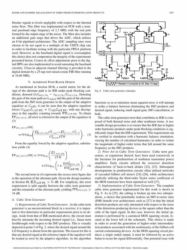
Fig. 9. Cubic term generator schematic.
functions so as to minimize mean squared error, it will attemptto strike a balance between eliminating the IM3 products anddesired signal, reducing small signal gain, IM3 cancellation, orboth.
The cubic term generator error that contributes to IER is com-posed of both thermal noise and other nonlinear terms. A rea-sonable design procedure is to ensure that the IER due to higherorder harmonic products under peak blocking conditions is sig-nificantly larger than the IER requirement. This requirement canbe verified in simulation with a harmonic balance simulation,varying the number of calculated harmonics in order to isolatethe magnitude of higher-order terms that fall around the samefrequency as the IM3 products.
2) Prior Art in Cubic Term Generators: Cubic term gen-erators, or expansions thereof, have been used extensively inthe literature for predistortion of nonlinear transmitter poweramplifiers. Early circuits utilized the crossover distortioncharacteristic of back-to-back diodes [22], [23]. Subsequentdevelopments in predistortion circuits often utilized networksof cascaded Gilbert cell mixers [24]–[26], while architecturesexplicitly utilizing the third-order Taylor series coefficient ofthe MOS transistor have been reported as well [27].
3) Implementation of Cubic Term Generator: The completecubic term generator implemented for this work is shown inFig. 9. As in [25], the cubing is broken up into two suboper-ations, a choice that potentially realizes an IM3-to-noise ratio(INR) benefit over architectures such as [27] in that the initialdistortion products are only attenuated with respect to the noiseof the distortion-producing devices as the square rather than thecube of the input signal. In this case, however, the initial op-eration is performed by a canonical MOS squaring circuit, lo-cated at the lower left of the schematic. This choice is madein order to avoid the generation of higher-order intermodula-tion products associated with the nonlinearity of the Gilbert cellcurrent commutating devices. As the MOS squaring circuit pro-duces a single ended output, it must be followed by an activebalun to recast the signal differentially. One potential issue with
Authorized licensed use limited to: CALIFORNIA INSTITUTE OF TECHNOLOGY. Downloaded on March 31, 2009 at 12:57 from IEEE Xplore. Restrictions apply.
2858 IEEE JOURNAL OF SOLID-STATE CIRCUITS, VOL. 43, NO. 12, DECEMBER 2008
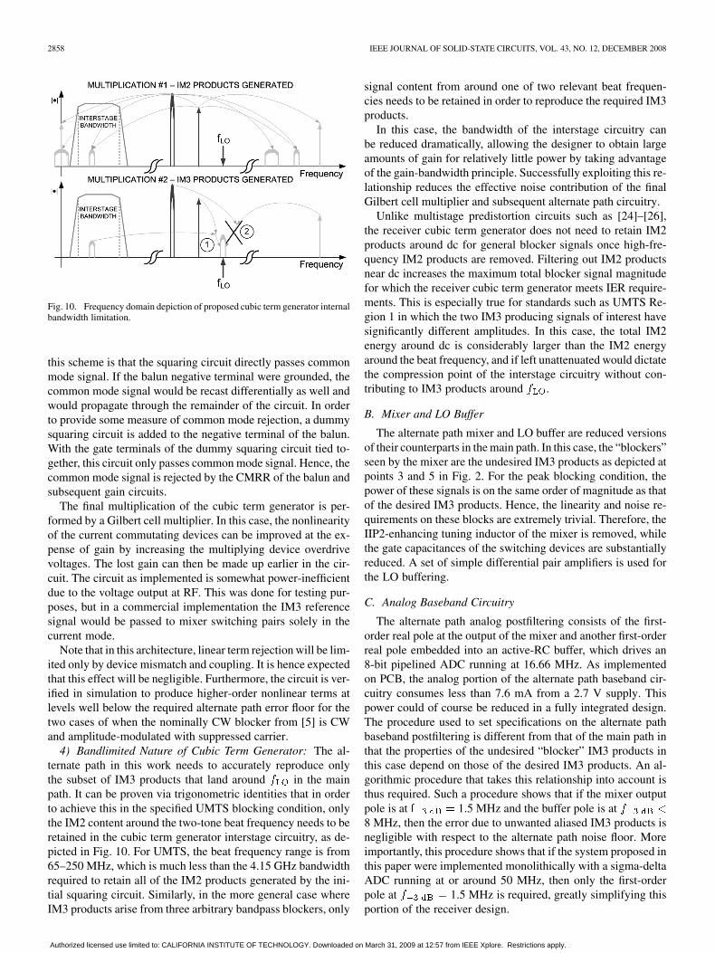
Fig. 10. Frequency domain depiction of proposed cubic term generator internalbandwidth limitation.
this scheme is that the squaring circuit directly passes commonmode signal. If the balun negative terminal were grounded, thecommon mode signal would be recast differentially as well andwould propagate through the remainder of the circuit. In orderto provide some measure of common mode rejection, a dummysquaring circuit is added to the negative terminal of the balun.With the gate terminals of the dummy squaring circuit tied to-gether, this circuit only passes common mode signal. Hence, thecommon mode signal is rejected by the CMRR of the balun andsubsequent gain circuits.
The final multiplication of the cubic term generator is per-formed by a Gilbert cell multiplier. In this case, the nonlinearityof the current commutating devices can be improved at the ex-pense of gain by increasing the multiplying device overdrivevoltages. The lost gain can then be made up earlier in the cir-cuit. The circuit as implemented is somewhat power-inefficientdue to the voltage output at RF. This was done for testing pur-poses, but in a commercial implementation the IM3 referencesignal would be passed to mixer switching pairs solely in thecurrent mode.
Note that in this architecture, linear term rejection will be lim-ited only by device mismatch and coupling. It is hence expectedthat this effect will be negligible. Furthermore, the circuit is ver-ified in simulation to produce higher-order nonlinear terms atlevels well below the required alternate path error floor for thetwo cases of when the nominally CW blocker from [5] is CWand amplitude-modulated with suppressed carrier.
4) Bandlimited Nature of Cubic Term Generator: The al-ternate path in this work needs to accurately reproduce onlythe subset of IM3 products that land around in the mainpath. It can be proven via trigonometric identities that in orderto achieve this in the specified UMTS blocking condition, onlythe IM2 content around the two-tone beat frequency needs to beretained in the cubic term generator interstage circuitry, as de-picted in Fig. 10. For UMTS, the beat frequency range is from65–250 MHz, which is much less than the 4.15 GHz bandwidthrequired to retain all of the IM2 products generated by the ini-tial squaring circuit. Similarly, in the more general case whereIM3 products arise from three arbitrary bandpass blockers, only
signal content from around one of two relevant beat frequen-cies needs to be retained in order to reproduce the required IM3products.
In this case, the bandwidth of the interstage circuitry canbe reduced dramatically, allowing the designer to obtain largeamounts of gain for relatively little power by taking advantageof the gain-bandwidth principle. Successfully exploiting this re-lationship reduces the effective noise contribution of the finalGilbert cell multiplier and subsequent alternate path circuitry.
Unlike multistage predistortion circuits such as [24]–[26],the receiver cubic term generator does not need to retain IM2products around dc for general blocker signals once high-fre-quency IM2 products are removed. Filtering out IM2 productsnear dc increases the maximum total blocker signal magnitudefor which the receiver cubic term generator meets IER require-ments. This is especially true for standards such as UMTS Re-gion 1 in which the two IM3 producing signals of interest havesignificantly different amplitudes. In this case, the total IM2energy around dc is considerably larger than the IM2 energyaround the beat frequency, and if left unattenuated would dictatethe compression point of the interstage circuitry without con-tributing to IM3 products around .
B. Mixer and LO Buffer
The alternate path mixer and LO buffer are reduced versionsof their counterparts in the main path. In this case, the “blockers”seen by the mixer are the undesired IM3 products as depicted atpoints 3 and 5 in Fig. 2. For the peak blocking condition, thepower of these signals is on the same order of magnitude as thatof the desired IM3 products. Hence, the linearity and noise re-quirements on these blocks are extremely trivial. Therefore, theIIP2-enhancing tuning inductor of the mixer is removed, whilethe gate capacitances of the switching devices are substantiallyreduced. A set of simple differential pair amplifiers is used forthe LO buffering.
C. Analog Baseband Circuitry
The alternate path analog postfiltering consists of the first-order real pole at the output of the mixer and another first-orderreal pole embedded into an active-RC buffer, which drives an8-bit pipelined ADC running at 16.66 MHz. As implementedon PCB, the analog portion of the alternate path baseband cir-cuitry consumes less than 7.6 mA from a 2.7 V supply. Thispower could of course be reduced in a fully integrated design.The procedure used to set specifications on the alternate pathbaseband postfiltering is different from that of the main path inthat the properties of the undesired “blocker” IM3 products inthis case depend on those of the desired IM3 products. An al-gorithmic procedure that takes this relationship into account isthus required. Such a procedure shows that if the mixer outputpole is at 1.5 MHz and the buffer pole is at8 MHz, then the error due to unwanted aliased IM3 products isnegligible with respect to the alternate path noise floor. Moreimportantly, this procedure shows that if the system proposed inthis paper were implemented monolithically with a sigma-deltaADC running at or around 50 MHz, then only the first-orderpole at 1.5 MHz is required, greatly simplifying thisportion of the receiver design.
Authorized licensed use limited to: CALIFORNIA INSTITUTE OF TECHNOLOGY. Downloaded on March 31, 2009 at 12:57 from IEEE Xplore. Restrictions apply.

KEEHR AND HAJIMIRI: EQUALIZATION OF THIRD-ORDER INTERMODULATION PRODUCTS 2859
Fig. 11. LMS concept and simulation: real LMS filter.
VI. DIGITAL EQUALIZATION
A. LMS-Based Adaptive Equalization
LMS-based adaptive equalizers are common choices forpower-constrained applications due to their simplicity androbustness [28]. In this project, the NLMS algorithm is uti-lized, as its convergence speed is potentially superior to thatof LMS [29]–[31]. The dynamics of the NLMS algorithm arealso much less sensitive to the properties of the input signalthan are those of LMS [28], [30], indicating more predictablebehavior over a wide range of conditions. The concept behindLMS-based adaptive equalization is depicted in Fig. 11. Here,a time-varying FIR filter is utilized to modify a reference signaland to subtract it from an incoming signal corrupted by aversion of the same reference signal. The taps of the FIR filterare adjusted based on the instantaneous correlation estimatebetween the equalizer output and the reference signal. That is,if there is any signal correlated with the reference signal in theequalizer output, each tap is adjusted on average in a directionso as to reduce the reference signal content in the output. Ifthe equalizer is designed properly, the filter taps will convergeclose to a solution that yields the minimum mean squaredoutput signal, but will exhibit a small excess error around thatsolution.
The operation of the two equalizers in their canonical com-plex form is described by (5), with bold symbols denotingcolumn vector quantities and the italicized portions corre-sponding to the NLMS algorithm alone
μ
μμ
(5)
When expanded into a physical hardware implementation, (5)takes the form of (6)–(8)
μμ
(6)
(7)
μ
μ (8)
Fig. 12. Simulated phase response of cubic term generator with respect to two-tone beat frequency.
The complex form of this algorithm is required for alternatepath distortion cancellation, as the phase relationship betweenthe main and alternate path signals is not fixed. To see why, con-sider the phase of the IM3 term generator as a function of theblocker two-tone beat frequency as shown in Fig. 12. As the beatfrequency changes, the adaptive filter must track the resultantrotational mismatch between the main and alternate paths. Notethat for this reason the adaptive filter tap values can not be deter-mined prior to the application of the IM3 producing blockers insuch a way as to facilitate accelerated algorithm convergence.
B. Fixed Versus Adaptive Equalization
Adaptive equalization of a known path difference is compu-tationally inefficient. The main reason for this is twofold. First,most analog path differences are IIR in nature, while adaptiveequalization algorithms such as those in the LMS family are FIRin nature. Second, even if the path difference were FIR, the LMSadaptive equalizer requires two multipliers per filter tap, as op-posed to just one for a fixed FIR filter. Hence, the known differ-ence between the main and alternate path transfer functions isequalized by fixed real three-multiplier IIR filters, as shown inFig. 4. The remaining path difference between the two paths is acomplex dc gain and a small random mismatch in the basebandtransfer function. This difference is broadband in the frequencydomain and by the duality principle will correspond to a smallnumber of taps required in the adaptive equalizer.
Authorized licensed use limited to: CALIFORNIA INSTITUTE OF TECHNOLOGY. Downloaded on March 31, 2009 at 12:57 from IEEE Xplore. Restrictions apply.
2860 IEEE JOURNAL OF SOLID-STATE CIRCUITS, VOL. 43, NO. 12, DECEMBER 2008
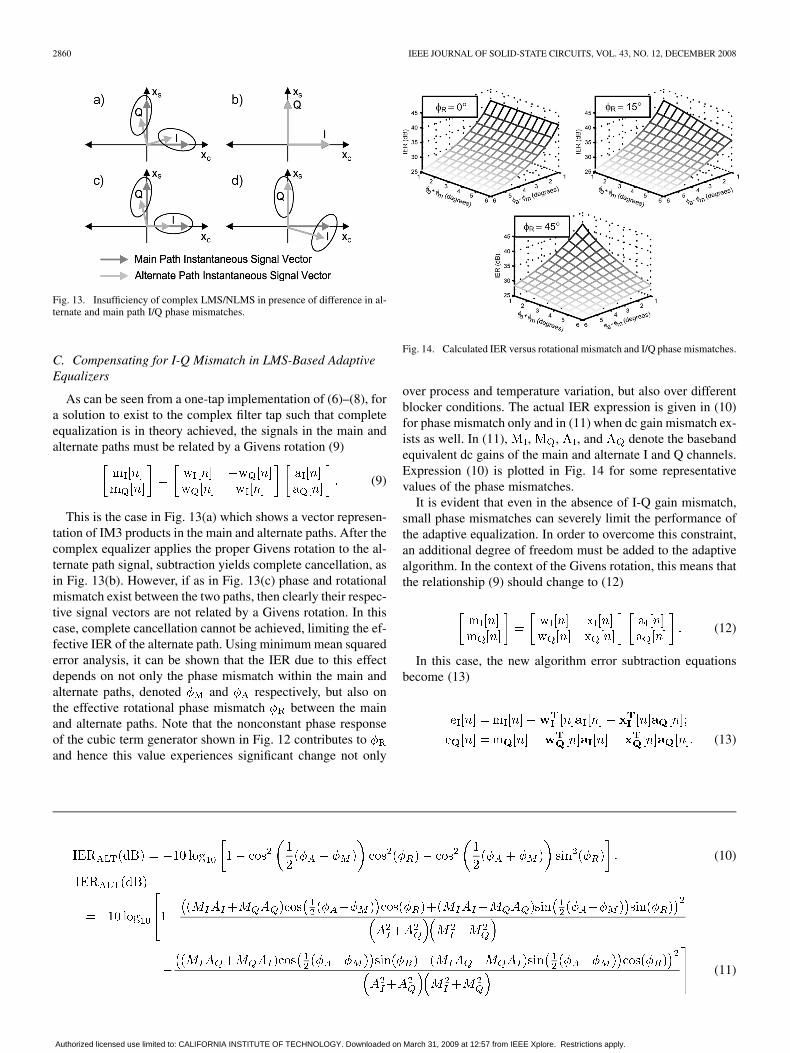
Fig. 13. Insufficiency of complex LMS/NLMS in presence of difference in al-ternate and main path I/Q phase mismatches.
C. Compensating for I-Q Mismatch in LMS-Based AdaptiveEqualizers
As can be seen from a one-tap implementation of (6)–(8), fora solution to exist to the complex filter tap such that completeequalization is in theory achieved, the signals in the main andalternate paths must be related by a Givens rotation (9)
(9)
This is the case in Fig. 13(a) which shows a vector represen-tation of IM3 products in the main and alternate paths. After thecomplex equalizer applies the proper Givens rotation to the al-ternate path signal, subtraction yields complete cancellation, asin Fig. 13(b). However, if as in Fig. 13(c) phase and rotationalmismatch exist between the two paths, then clearly their respec-tive signal vectors are not related by a Givens rotation. In thiscase, complete cancellation cannot be achieved, limiting the ef-fective IER of the alternate path. Using minimum mean squarederror analysis, it can be shown that the IER due to this effectdepends on not only the phase mismatch within the main andalternate paths, denoted and respectively, but also onthe effective rotational phase mismatch between the mainand alternate paths. Note that the nonconstant phase responseof the cubic term generator shown in Fig. 12 contributes toand hence this value experiences significant change not only
Fig. 14. Calculated IER versus rotational mismatch and I/Q phase mismatches.
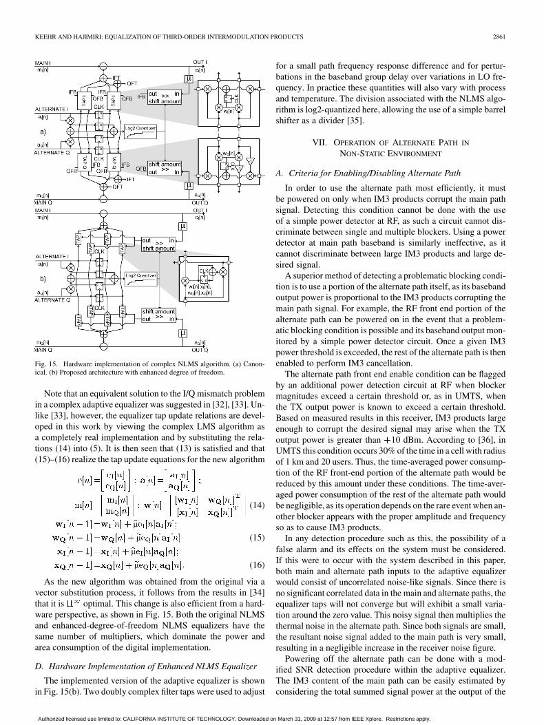
over process and temperature variation, but also over differentblocker conditions. The actual IER expression is given in (10)for phase mismatch only and in (11) when dc gain mismatch ex-ists as well. In (11), , , , and denote the basebandequivalent dc gains of the main and alternate I and Q channels.Expression (10) is plotted in Fig. 14 for some representativevalues of the phase mismatches.
It is evident that even in the absence of I-Q gain mismatch,small phase mismatches can severely limit the performance ofthe adaptive equalization. In order to overcome this constraint,an additional degree of freedom must be added to the adaptivealgorithm. In the context of the Givens rotation, this means thatthe relationship (9) should change to (12)
(12)
In this case, the new algorithm error subtraction equationsbecome (13)
(13)
(10)
(11)
Authorized licensed use limited to: CALIFORNIA INSTITUTE OF TECHNOLOGY. Downloaded on March 31, 2009 at 12:57 from IEEE Xplore. Restrictions apply.
KEEHR AND HAJIMIRI: EQUALIZATION OF THIRD-ORDER INTERMODULATION PRODUCTS 2861
Fig. 15. Hardware implementation of complex NLMS algorithm. (a) Canon-ical. (b) Proposed architecture with enhanced degree of freedom.
Note that an equivalent solution to the I/Q mismatch problemin a complex adaptive equalizer was suggested in [32], [33]. Un-like [33], however, the equalizer tap update relations are devel-oped in this work by viewing the complex LMS algorithm asa completely real implementation and by substituting the rela-tions (14) into (5). It is then seen that (13) is satisfied and that(15)–(16) realize the tap update equations for the new algorithm
(14)
μ
μ (15)
μ
μ (16)
As the new algorithm was obtained from the original via avector substitution process, it follows from the results in [34]that it is optimal. This change is also efficient from a hard-ware perspective, as shown in Fig. 15. Both the original NLMSand enhanced-degree-of-freedom NLMS equalizers have thesame number of multipliers, which dominate the power andarea consumption of the digital implementation.
D. Hardware Implementation of Enhanced NLMS Equalizer
The implemented version of the adaptive equalizer is shownin Fig. 15(b). Two doubly complex filter taps were used to adjust
for a small path frequency response difference and for pertur-bations in the baseband group delay over variations in LO fre-quency. In practice these quantities will also vary with processand temperature. The division associated with the NLMS algo-rithm is log2-quantized here, allowing the use of a simple barrelshifter as a divider [35].
VII. OPERATION OF ALTERNATE PATH IN
NON-STATIC ENVIRONMENT
A. Criteria for Enabling/Disabling Alternate Path
In order to use the alternate path most efficiently, it mustbe powered on only when IM3 products corrupt the main pathsignal. Detecting this condition cannot be done with the useof a simple power detector at RF, as such a circuit cannot dis-criminate between single and multiple blockers. Using a powerdetector at main path baseband is similarly ineffective, as itcannot discriminate between large IM3 products and large de-sired signal.
A superior method of detecting a problematic blocking condi-tion is to use a portion of the alternate path itself, as its basebandoutput power is proportional to the IM3 products corrupting themain path signal. For example, the RF front end portion of thealternate path can be powered on in the event that a problem-atic blocking condition is possible and its baseband output mon-itored by a simple power detector circuit. Once a given IM3power threshold is exceeded, the rest of the alternate path is thenenabled to perform IM3 cancellation.
The alternate path front end enable condition can be flaggedby an additional power detection circuit at RF when blockermagnitudes exceed a certain threshold or, as in UMTS, whenthe TX output power is known to exceed a certain threshold.Based on measured results in this receiver, IM3 products largeenough to corrupt the desired signal may arise when the TXoutput power is greater than 10 dBm. According to [36], inUMTS this condition occurs 30% of the time in a cell with radiusof 1 km and 20 users. Thus, the time-averaged power consump-tion of the RF front-end portion of the alternate path would bereduced by this amount under these conditions. The time-aver-aged power consumption of the rest of the alternate path wouldbe negligible, as its operation depends on the rare event when an-other blocker appears with the proper amplitude and frequencyso as to cause IM3 products.
In any detection procedure such as this, the possibility of afalse alarm and its effects on the system must be considered.If this were to occur with the system described in this paper,both main and alternate path inputs to the adaptive equalizerwould consist of uncorrelated noise-like signals. Since there isno significant correlated data in the main and alternate paths, theequalizer taps will not converge but will exhibit a small varia-tion around the zero value. This noisy signal then multiplies thethermal noise in the alternate path. Since both signals are small,the resultant noise signal added to the main path is very small,resulting in a negligible increase in the receiver noise figure.
Powering off the alternate path can be done with a mod-ified SNR detection procedure within the adaptive equalizer.The IM3 content of the main path can be easily estimated byconsidering the total summed signal power at the output of the
Authorized licensed use limited to: CALIFORNIA INSTITUTE OF TECHNOLOGY. Downloaded on March 31, 2009 at 12:57 from IEEE Xplore. Restrictions apply.

2862 IEEE JOURNAL OF SOLID-STATE CIRCUITS, VOL. 43, NO. 12, DECEMBER 2008
equalizer taps. Comparing this quantity to the total power ofthe equalizer output yields an estimate of the desired signal toIM3 product ratio. When this ratio is high enough, the base-band portion of the alternate path can be turned off. Becausethis SNR estimate can fluctuate under fading conditions, a min-imum on-time can be instituted for the alternate path basebandcircuitry such that it does not toggle on and off repeatedly withina single blocking incident.
B. DC Offset Issues During Alternate Path Enabling andSolution
As is well-known, direct conversion receivers are susceptibleto large dc offsets at baseband [16], [20]. This presents an issuewith regards to the adaptive filter in that if both dc offset andIM3 signal are present on both main and alternate paths, theadaptive equalizer will attempt to equalize both signals. How-ever, because the dc offset is large and uncorrelated with thepath mismatch at dc, the optimal transfer function of the adap-tive equalizer will have a large impulse at dc in the frequencydomain. In the time domain, this corresponds to a very largenumber of adaptive filter taps, which will consume inordinateamounts of power and degrade the performance of the equalizer[28].
A common solution to the dc offset issue in UMTS receiversis to use high-pass filtering at baseband [7], [8], [37], with acutoff frequency no greater than 10 kHz [37]. In this work,high-pass filtering at 10 kHz is performed in the digital domainfor both main and alternate paths to remove the dc offset of thecomplete analog portion of the receiver, including the ADC. Theproblem with doing this in either domain, however, is that whenthe alternate path powers on, the dc offset of the mixer appearsas a step to the alternate path high pass filter. Because the cutofffrequency of the HPF is low, the resultant step response takes3–4 time constants to settle below the error floor, thus preventingconvergence of the adaptive filter during this time. Another op-tion is to adaptively remove dc offset as part of the equalizeralgorithm [2], [38]. However, it can be shown that this tech-nique effectively implements a high-pass filter and would havethe same settling time issue.
The solution utilized in this work to remove this startup tran-sient is to retain the high-pass filters mentioned earlier, but toalso power on the alternate path baseband circuitry and mea-sure the dc offset in the digital domain in the absence of IM3products being passed through the alternate path. This measure-ment is then immediately subtracted from the incoming signalto remove the dc offset. Since the only signals present at thistime are dc offset and a small amount of noise, these operationscan be performed relatively quickly (a few microseconds) bya simple averaging circuit, permitting periodic dc offset mea-surements while the alternate path front end is enabled for IM3product detection. The complete scheme is depicted in Fig. 16.DC offset correction can be performed in the main path as well,but was forgone in order to simplify the experiment.
C. Behavior of System in a Fading Environment
The adaptive equalizer in the architecture presented hereinexists mainly to compensate for unknown circuit mismatchesand the effective rotational phase difference between the main
Fig. 16. Alternate path dc offset correction procedure.
Fig. 17. Modified two tone test concept.
and alternate paths. However, the adaptive equalizer may alsoneed to track slightly to compensate for changing blocker char-acteristics as a result of fading. Considering that most IM3-pro-ducing blockers for UMTS are clustered around 2 GHz, andassuming that the maximum speed of the mobile terminal is250 km/h, the minimum coherence time of the blockers is about400 s [39] (note: for this experiment 0 dB, 21.1 dB).The adaptive equalizer needs to be able to converge faster thanthis amount in order to properly track the changing IM3 prod-ucts, a requirement that is not difficult to meet.
VIII. EXPERIMENTAL RESULTS
A. Receiver IIP3 Measurement Results
Fig. 17 shows the concept behind the modified two-tone IIP3test used to evaluate the IM3 equalization. The goal is to repro-duce the TX leakage and CW blocker signals at the LNA inputat several magnitudes (including the worst-case specified), at all12 UMTS RX frequencies and to measure the output across theRX band in each instance. The TX signal model is a QPSK-mod-ulated pseudorandom noise bit sequence (PN23) at 3.84 MSPSthat is upsampled, passed through the UMTS-specified channelfilter, and upconverted to 1.98 GHz. The CW magnitude is fixedat 8 dB less than that of the TX. The resultant steady-state errorover swept TX leakage magnitude for 2.1225 GHz isshown in Fig. 18(a). Note that all plots shown and numbers re-ported depict the I/Q receiver channel with worst-case perfor-mance under worst-case specified blocking. The total input-re-ferred error accounts for gain loss, thermal noise, and all IMproducts. Removing the effects of main path thermal noise andIM2 products yields a lumped input-referred error quantity con-sisting of all other error sources. From this quantity, which istreated as residual IM3 error, a slope-of-3 line is extrapolatedfrom the worst-case input blocker magnitude to obtain an ef-fective IIP3 metric. Other measurement results show that thecorrected IIP3 performance is limited by higher-order distortionproducts in the main path. Note that 50 kTB noise is removedfrom these plots and that the maximum total input-referred errorin this regard, computed in Section III-B ( 98.2 dB) under the
Authorized licensed use limited to: CALIFORNIA INSTITUTE OF TECHNOLOGY. Downloaded on March 31, 2009 at 12:57 from IEEE Xplore. Restrictions apply.

KEEHR AND HAJIMIRI: EQUALIZATION OF THIRD-ORDER INTERMODULATION PRODUCTS 2863
Fig. 18. Measured results of modified two tone test. (a) For proposed enhanced complex NLMS architecture. (b) For canonical complex NLMS architecture.
Fig. 19. Measured results of modified two tone testing which IM3 products contain squared TX leakage.
worst-case scenario of 26 dBm TX leakage, is met with 3 dBof margin when correction is applied. The contribution of thebaseband circuitry to the uncorrected IIP3 has also been mea-sured and found to be negligible.
In Fig. 18(b) are the results of this same test using the NLMSalgorithm without the enhanced degree of freedom. A phasemismatch of about 3 in the main path along with mismatch inthe baseband frequency responses are responsible for the higherinput-referred IM3 products. This confirms experimentally thatthis design enhancement produces a noticeable performance im-provement for this design.
Although the uncorrected IIP3 of the receiver happens to besufficient to handle the scenario in which the CW blocker fre-quency is less than the TX frequency, the CW blocker amplitudewas exaggerated far above specification in order to show thatthis case is covered by the proposed architecture as well. Thiscase generates an IM3 product consisting of a frequency-trans-lated version of the squared modulated TX signal in the mainpath. It is worthwhile to measure these results, as this conditionis subject to an additional error term resulting from the bandlim-ited nature of the cubic term generator. Specifically, the alternatepath output is not squared TX leakage but rather the modulatedTX leakage multiplied by a delayed version of itself. The re-
sults of this test are shown in Fig. 19 for 1.8375 GHzand 2.1225 GHz and show similar correction ratios tothose seen in Fig. 18(a).
The experiment performed for Fig. 18(a) is repeated acrossthe UMTS RX band, with the results shown in Fig. 20. TheTX frequency is kept at 1.98 GHz and the CW frequency ad-justed so that the IM3 products land within the RX band. Con-vergence behavior of the adaptive equalizer is shown in Fig. 21for the case where 2.1225 GHz. It is seen that if dcoffset correction is not applied prior to the enabling of the alter-nate path digital back end, the convergence time is dramaticallyextended, as expected. The frequency-domain measurement ofthe digital receiver output in the presence of a moderately largetonal desired signal is shown in Fig. 22 both with and withoutcorrection.
B. Receiver Sensitivity Measurement Results
The actual specification that must be met for UMTS is thatof the sensitivity test, whose results are often predicted frominput-referred error tests by the relations described in [7],[17], [39]. With 1.8 dB the receiver must achieve
for 118.8 dBm at the LNAinput under typical conditions and 115.8 dBm
Authorized licensed use limited to: CALIFORNIA INSTITUTE OF TECHNOLOGY. Downloaded on March 31, 2009 at 12:57 from IEEE Xplore. Restrictions apply.

2864 IEEE JOURNAL OF SOLID-STATE CIRCUITS, VOL. 43, NO. 12, DECEMBER 2008
Fig. 20. Measured results of modified two tone test for �26 dBm TX leakage, �34 dBm CW blocker swept over LO frequency.
Fig. 21. Measured convergence behavior of adaptive equalization algorithm.
Fig. 22. Digital spectrum analyzer (Agilent 89601 VSA) measurements—Correction in presence of modulated IM3, tonal desired signal. (a) Full outputspectrum. (b) Zoomed in.
under worst-case blocking. The results of such a test on thereceiver described in this paper at 2.1225 GHz withboth I and Q channels active are shown in Fig. 23. The inputused is a specification-equivalent UMTS 12.2 kbps downlinkreference measurement channel [5], and the measurement re-sults obtained are comparable to those presented in [7]. Eachpoint in Fig. 23 represents the average of bits(2000 data frames), which is sufficient to accurately re-solve BER down to [40]. The baseline sensitivity is
121.9 dBm, 0.5 dB greater than predicted by the measured
noise figure, with the discrepancy accounted for by unfilterednoise at frequencies greater than 1.92 MHz. The sensitivityof the receiver under worst-case blocking and correction is
119.5 dBm, 0.9 dB greater than predicted by total input-re-ferred error, with 0.6 dB of this difference accounted for bynoise at frequencies greater than 1.92 MHz. This shows thatthe total input-referred corrected error curve from Fig. 20 isan accurate predictor of the actual sensitivity performance.Without correction, sensitivity significantly exceeds specifica-tion at 98.8 dBm under blocking.
Authorized licensed use limited to: CALIFORNIA INSTITUTE OF TECHNOLOGY. Downloaded on March 31, 2009 at 12:57 from IEEE Xplore. Restrictions apply.
KEEHR AND HAJIMIRI: EQUALIZATION OF THIRD-ORDER INTERMODULATION PRODUCTS 2865
Fig. 23. Measured receiver DPCH SNR and BER under sensitivity, sensitivity/blocking/correction, and sensitivity/blocking/no correction, respectively.
Fig. 24. Measured INR performance of alternate path.
C. Alternate Path Measurement Results
The IM3-to-noise ratio (INR) performance of the alternatepath for is measured up to the equalizer inputand shown in Fig. 24. Performance under worst-case specifiedblocking conditions at 2.1225 GHz is 31 dB. Addi-tional measurements suggest that higher order distortion prod-ucts lower IER from INR by less than 1 dB. Alternate pathlinear term feedthrough is also measured and referred to themain path input. The attenuation referred to the main path inputis found to be greater than 46 dB over all LO frequencies, indi-cating that the effect of these terms in the equalization processis negligible.
D. Additional Measurement Results
The RF front end die photo is shown in Fig. 25. The per-formance summary for the system and front end is shown inTable II. Note that these and all other quoted results differ fromthose reported in [41] due to improvements made to the systemto permit acceptable operation across the entire RX band. Thenew power consumption estimate of the alternate path digitalback end circuitry was obtained from switching statistics ofa gate-level Verilog simulation referencing a 90-nm CMOSprocess standard cell library.
Fig. 25. RF front end die photo.
IX. CONCLUSION
This paper has presented a receiver architecture that utilizesa nonlinear mixed-signal alternate feedforward receiver pathextending into the RF domain, and shows that it dramaticallyimproves the IIP3 performance of an integrated SAW-lessUMTS receiver front end. An internally bandlimited RF cubicterm generator was described and successfully implementedin order to provide a suitable reference signal for equalization.Implications regarding the design of the other alternate pathcircuitry, including the digital adaptive equalization, were alsoexamined. Furthermore, a technique to deal with the interactionof dc offset and adaptive equalization while maintaining a rel-atively small convergence time is described and demonstrated.The excess power consumption drawn by the alternate receiverpath is small over time-averaging, as it needs only to be fullyenabled in the rare event that an IM3-producing blockingcondition exists.
Authorized licensed use limited to: CALIFORNIA INSTITUTE OF TECHNOLOGY. Downloaded on March 31, 2009 at 12:57 from IEEE Xplore. Restrictions apply.
2866 IEEE JOURNAL OF SOLID-STATE CIRCUITS, VOL. 43, NO. 12, DECEMBER 2008
TABLE IIMEASURED PERFORMANCE SUMMARY
ACKNOWLEDGMENT
The authors would like to thank F. Bohn for the frequencydivider IP and testing assistance from H. Mani and J. Yoo, allof Caltech. They would also like to thank Prof. A. Emami,Prof. B. Hassibi, Prof. V. Pedroni, H. Wang, Y. Wang, F. Bohn,S. Jeon, A. Babakhani, J. Chen, and M. Loh of Caltech, andS. Kousai of Toshiba for their help and advice.
REFERENCES
[1] L. Yu and M. Snelgrove, “Signal processor for reducing undesirablesignal content,” U.S. Patent 6 804 359, Oct. 12, 2004.
[2] M. Faulkner, “DC offset and IM2 removal in direct conversion re-ceivers,” IEE Proc. Commun., vol. 149, pp. 179–184, Jun. 2002.
[3] V. H. Estrick and R. T. Siddoway, “Receiver distortion circuit andmethod,” U.S. Patent 5 237 332, Aug. 17, 1993.
[4] M. Valkama, A. S. H. Ghadam, L. Antilla, and M. Renfors, “Advanceddigital signal processing techniques for compensation of nonlinear dis-tortion in wideband multicarrier radio recivers,” IEEE Trans. Microw.Theory Techn., vol. 54, no. 6, pp. 2356–2366, Jun. 2006.
[5] UE Radio Transmission and Reception (FDD), Tech. SpecificationGroup, “3GPP, (TSG) RAN WG4, TS 25.101, v8.1.0,” , Dec. 2007.
[6] B. A. Floyd, S. K. Reynolds, T. Zwick, L. Khuon, T. Beukema, andU. R. Pfeiffer, “WCDMA direct-conversion receiver front-end compar-ison in RF-CMOS and SiGe BiCMOS,” IEEE Trans. Microw. TheoryTechn., vol. 53, no. 4, pp. 1181–1188, Apr. 2002.
[7] S. K. Reynolds, B. A. Floyd, T. J. Beukema, T. Zwick, and U. R.Pfeiffer, “Design and compliance testing of a SiGe WCDMA receiverIC with integrated analog baseband,” Proc. IEEE, vol. 93, no. 9, pp.1624–1636, Sep. 2005.
[8] D. Kaczman, M. Shah, N. Godambe, M. Alam, H. Guimaraes, L. M.Han, M. Rachedine, D. L. Cashen, W. E. Getka, C. Dozier, W. P. Shep-herd, and K. Couglar, “A single-chip tri-band (2100, 1900, 850/800MHz) WCDMA/HSDPA cellular transceiver,” IEEE J. Solid-State Cir-cuits, vol. 41, no. 5, pp. 1122–1132, May 2006.
[9] M. Tamura, T. Nakayama, Y. Hino, A. Yoshizawa, and K. Takagi, “Alow voltage (1.8 V) operation triple band WCDMA transceiver IC,” inProc. IEEE RFIC Symp., Jun. 2005, pp. 269–272.
[10] N. K. Yanduru, D. Griffith, S. Bhagavatheeswaran, D. Griffith, S.Bhagavatheeswaran, C.-C. Chen, F. Dulger, S.-J. Fang, Y.-C. Ho,and K.-M. Low, “A WCDMA, GSM/GPRS/EDGE receiver front endwithout interstage SAW filter,” in Proc. IEEE RFIC Symp., Jun. 2006,pp. 19–22.
[11] B. Tenbroek, J. Strange, D. Nalbantis, C. Jones, P. Fowers, S. Brett, C.Beghein, and F. Beffa, “Single-chip tri-band WCDMA/HSDPA trans-ceiver without external SAW filters and with integrated TX power con-trol,” in IEEE Int. Solid-State Circuits Conf. (ISSCC) Dig. Tech. Papers,Feb. 2008, pp. 202–203.
[12] A. Safarian, A. Shameli, A. Rofougaran, M. Rofougaran, and F. deFlaviis, “Integrated blocker filtering RF front ends,” in IEEE RFICSymp. Dig. Tech Papers, Jun. 2007, pp. 13–16.
[13] V. Aparin, G. J. Ballantyne, C. J. Persico, and A. Cicalini, “An in-tegrated LMS adaptive filter of TX leakage for CDMA receiver frontends,” IEEE J. Solid-State Circuits, vol. 41, no. 5, pp. 1171–1182, May2006.
[14] M. Brandolini, P. Rossi, D. Sanzogni, and F. Svelto, “A �78 dBmIIP2 CMOS direct downconversion mixer for fully integrated UMTSreceivers,” IEEE J. Solid-State Circuits, vol. 41, no. 3, pp. 552–559,Mar. 2006.
[15] A. Liscidini, M. Brandolini, D. Sanzogni, and R. Castello, “A 0.13mm CMOS front-end for DCS1800/UMTS/802.11b-g with multibandpositive feedback low-noise amplifier,” IEEE J. Solid-State Circuits,vol. 41, no. 4, pp. 981–989, Apr. 2006.
[16] H. J. Bergveld, K. M. M. van Kaam, D. M. W. Leenaerts, K. J. P.Philips, A. W. P. Vaassen, and G. Wetkzer, “A low-power highly digi-tized receiver for 2.4-GHz-band GFSK applications,” IEEE Trans. Mi-crow. Theory Techn., vol. 53, pp. 453–461, Feb. 2005.
[17] B. J. Minnis and P. A. Moore, “A highly digitized multimode receiverarcitecture for 3G mobiles,” IEEE Trans. Veh. Technol., vol. 52, no. 5,pp. 637–653, May 2003.
[18] muRata Corp., Data sheet, Part # DFYK61G95LBJCA [Online]. Avail-able: http://www.murata.com,
[19] A. Springer, L. Maurer, and R. Weigel, “RF system concepts for highlyintegrated RFICs for W-CDMA mobile radio terminals,” IEEE Trans.Microw. Theory Techn., vol. 50, no. 1, pp. 254–267, Jan. 2002.
[20] B. Razavi, RF Microelectronics. Upper Saddle River, NJ: Prentice-Hall, 1998.
[21] R. Magoon, A. Molnar, J. Zachan, G. Hatcher, and W. Rhee, “A single-chip quad-band (850/900/1800/1900 MHz) direct conversion GSM/GPRS RF transceiver with integrated VCOs and fractional-N synthe-sizer,” IEEE J. Solid-State Circuits, vol. 37, no. 12, pp. 1710–1720,Dec. 2002.
[22] T. Nojima and N. Konno, “Cuber predistortion linearizer for relayequipment in 800 MHz band land mobile telephone system,” IEEETrans. Veh. Technol., vol. VT-34, no. 11, pp. 169–177, Nov. 1985.
[23] N. Imai, T. Nojima, and T. Murase, “Novel linearizer using balancedcirculators and its application to multilevel digital radio systems,” IEEETrans. Microw. Theory Techn., vol. 37, no. 8, pp. 1237–1243, Aug.1989.
[24] E. Westesson and L. Sundstrom, “A complex polynomial predistorterchip in CMOS for baseband or IF linearization of RF power amplifiers,”in Proc. IEEE Int. Symp. Circuits Syst. (ISCAS), Jun. 1999, vol. 1, pp.206–209.
[25] T. Nesimoglu, C. N. Canagarajah, and J. P. McGeehan, “A broad-band polynomial predistorter for reconfigurable radio,” in Proc. Veh.Technol. Conf., May 2001, vol. 3, pp. 1968–1972.
[26] T. Rahkonen, O. Kursu, M. Riikola, J. Aikio, and T. Tuikkanen, “Per-formance of an integrated 2.1 GHz analog predistorter,” in Proc. Int.Workshop Integr. Nonlinear Microw. Millimeter-Wave Circuits, Jan.2006, pp. 34–37.
[27] F. Shearer and L. MacEachern, “A precision CMOS analog cubing cir-cuit,” in Proc. IEEE NEWCAS, Jun. 2004, pp. 281–284.
[28] S. Haykin, Adaptive Filter Theory. Upper Saddle River, NJ: Prentice-Hall, 2002, ch. 5.
[29] M. Tarrab and A. Feuer, “Convergence and performance analysis ofthe normalized LMS algorithm with uncorrelated Gaussian data,” IEEETrans. Inf. Theory, vol. 34, no. 7, pp. 680–691, Jul. 1988.
[30] D. T. M. Slock, “On the convergence behavior of the LMS and normal-ized LMS algorithms,” IEEE Trans. Signal Process., vol. 41, no. 9, pp.2811–2825, Sep. 1993.
[31] V. H. Nascimento, “A simple model for the effect of normalization onthe convergence rate of adaptive filters,” in IEEE Int. Conf. Acoust.,Speech, Signal Process. (ICASSP) Dig. Tech. Papers, May 2004, vol.2, pp. 453–6.
[32] K. Gerlach, “The effect of I,Q mismatch errors on adaptive cancella-tion,” IEEE Trans. Aerosp. Electron. Syst., vol. 28, no. 3, pp. 729–740,Jul. 1992.
[33] K. Gerlach and M. J. Steiner, “An adaptive matched filter that compen-sates for I, Q mismatch errors,” IEEE Trans. Signal Process., vol. 45,no. 12, pp. 3104–3107, Dec. 1997.
Authorized licensed use limited to: CALIFORNIA INSTITUTE OF TECHNOLOGY. Downloaded on March 31, 2009 at 12:57 from IEEE Xplore. Restrictions apply.

KEEHR AND HAJIMIRI: EQUALIZATION OF THIRD-ORDER INTERMODULATION PRODUCTS 2867
[34] B. Hassibi, A. H. Sayed, and T. Kailath, “ � optimality of the LMSalgorithm,” IEEE Trans. Signal Process., vol. 44, no. 2, pp. 267–280,Feb. 1996.
[35] H. Oba, M. Kim, and H. Arai, “FPGA implementation of LMS andN-LMS processor for adaptive array applications,” in Int. Symp. In-telligent Signal Process. Commun. (ISPACS) Dig. Tech. Papers, Dec.2006, pp. 485–488.
[36] M. Schwab and P. Seidenberg, “Analysis of mobile-originated interfer-ence in coexisting UMTS networks,” in Proc. Veh. Technol. Conf., May2002, vol. 4, pp. 1636–1639.
[37] J. Rogin, I. Kouchev, G. Brenna, D. Tschopp, and Q. Huang, “A 1.5-V45-mW direct-conversion WCDMA receiver IC in 0.13- �m CMOS,”IEEE J. Solid-State Circuits, vol. 38, no. 12, pp. 2239–2248, Dec. 2003.
[38] L. Der and B. Razavi, “A 2-GHz CMOS image-reject receiver withLMS calibration,” IEEE J. Solid-State Circuits, vol. 38, no. 2, pp.167–175, Feb. 2003.
[39] A. Springer and R. Weigel, UMTS: The Physical Layer of theUniversal Mobile Telecommunications System. Berlin, Germany:Springer-Verlag, 2002, pp. 34–40.
[40] M. Jeruchim, “Techniques for estimating the bit error rate in the simu-lation of digital communication systems,” IEEE J. Sel. Areas Commun.,vol. SAC-2, no. 1, pp. 153–170, Jan. 1984.
[41] E. Keehr and A. Hajimiri, “Equalization of IM3 products in widebanddirect-conversion receivers,” in IEEE Int. Solid-State Circuits Conf.(ISSCC) Dig. Tech. Papers, Feb. 2008, pp. 204–205.
Edward A. Keehr (M’02–S’05) received the S.B.and M.Eng degrees in electrical engineering from theMassachusetts Institute of Technology (MIT), Cam-bridge, in 2001 and 2002, respectively. He is cur-rently working towards the Ph.D. degree in electricalengineering with the Caltech High-Speed IntegratedCircuits (CHIC) Group, California Institute of Tech-nology (Caltech), Pasadena.
From 1999 to 2002, he held summer internshipswith QUALCOMM, Incorporated, San Diego, CA aspart of the MIT VI-A internship program. From 2002
to 2005, he worked at QUALCOMM as a full-time Design Engineer specializingin analog and mixed-signal circuits. His current research interests include RFtransceiver circuits and architectures.
Mr. Keehr was a recipient of an NDSEG Fellowship in 2005 and the AnalogDevices Outstanding Student Designer Award in 2006. He is a member of TauBeta Pi and Eta Kappa Nu.
Ali Hajimiri (M’99) received the B.S. degree inelectronics engineering from the Sharif Universityof Technology, Tehran, Iran, in 1996, and the M.S.and Ph.D. degrees in electrical engineering fromStanford University, Stanford, CA, in 1998.
He was a Design Engineer with Philips Semicon-ductors, where he worked on a BiCMOS chipset forGSM and cellular units from 1993 to 1994. In 1995,he was with Sun Microsystems, where he worked onthe UltraSPARC microprocessor’s cache RAM de-sign methodology. During the summer of 1997, he
was with Lucent Technologies–Bell Labs, Murray Hill, NJ, where he inves-tigated low-phase-noise integrated oscillators. In 1998, he joined the Facultyof the California Institute of Technology, Pasadena, where he is a Professor ofElectrical Engineering and the director of Microelectronics Laboratory. His re-search interests include high-speed and RF integrated circuits. He is the authorof The Design of Low Noise Oscillators (Springer, 1999) and has authored andcoauthored more than 100 refereed journal and conference technical articles. Heholds more than 30 U.S. and European patents.
Dr. Hajimiri is a member of the Technical Program Committee of the In-ternational Solid-State Circuits Conference (ISSCC). He has also served as anAssociate Editor of the IEEE JOURNAL OF SOLID-STATE CIRCUITS, an Asso-ciate Editor of IEEE TRANSACTIONS ON CIRCUITS AND SYSTEMS—PART II:EXPRESS BRIEFS, a member of the Technical Program Committees of the In-ternational Conference on Computer Aided Design (ICCAD), Guest Editor ofthe IEEE TRANSACTIONS ON MICROWAVE THEORY AND TECHNIQUES, and theGuest Editorial Board of Transactions of Institute of Electronics, Informationand Communication Engineers of Japan (IEICE). He was selected to the top100 innovators (TR100) list in 2004 and is a Fellow of Okawa Foundation.He is a Distinguished Lecturer of the IEEE Solid-State and Microwave Soci-eties. He is the recipient of Caltech’s Graduate Students Council Teaching andMentoring award as well as Associated Students of Caltech Undergraduate Ex-cellence in Teaching Award. He was the Gold medal winner of the NationalPhysics Competition and the Bronze Medal winner of the 21st InternationalPhysics Olympiad, Groningen, Netherlands. He was a co-recipient of the IEEEJOURNAL OF SOLID-STATE CIRCUITS Best Paper Award of 2004, the InternationalSolid-State Circuits Conference (ISSCC) Jack Kilby Outstanding Paper Award,two times co-recipient of CICC’s best paper awards, and a three times winnerof the IBM faculty partnership award as well as National Science FoundationCAREER Award. He is a cofounder of Axiom Microdevices Inc.
Authorized licensed use limited to: CALIFORNIA INSTITUTE OF TECHNOLOGY. Downloaded on March 31, 2009 at 12:57 from IEEE Xplore. Restrictions apply.