Embed Size (px)
Citation preview
6 RAYTHEON CO QUINCY MASS INDUSTRIAL COMPONENTS OPERATIO F/6 ,MANUFACTURING METHODS AND TECHNOLOGY ENGINEERING IMW AND TE) PR--FTCIl)APR 80 R M ZIL ERSTEIN CAA07-76-C-811
UNCLASSIFIED OELET-TR-76-81 q-F-VOL-2 NL
IEE
Hll 332__.o~
1111["2--5 IIIII 1 811jj.25 IIi 4 JflI6
MICROCOPY RESOLUTION TEST CHARTNAT ONA L BU REAU O STANDARDS 1963-A
EL&
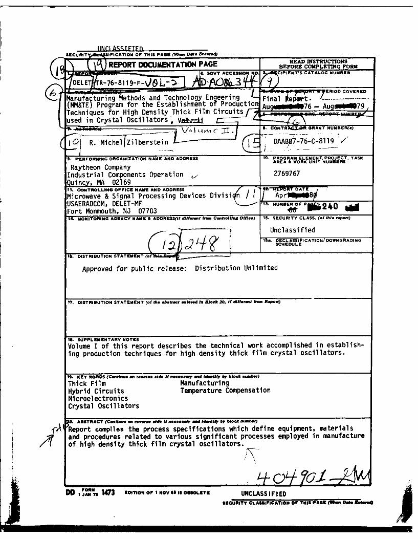
Research and Development Technical ReportDELET-TR-76-8119-F
MANUFACTURING METHODS AND TECHNOLOGY ENGINEERING(MM &TE) PROGRAM FOR THE ESTABLISHMENT OF PRODUC-TION TECHNIQUES FOR HIGH DENSITY THICK FILM CIRCUITSUSED IN CRYSTAL OSCILLATORS
zVOLUME II
0 R. Michel Zilberstein
qc RAYTHEON COMPANY "Industrial Components Operation (Quincy, MA 0Z169
April 1980
Final Report for Period August 1976 - August 1979
DISTRIBUTION STATEMENT
Approved for public release; distribution unlimited.
Prepared for:
ELECTRONICS TECHNOLOGY AND DEVICES LABORATORY
, ERADCOMUS ARMY ELECTRONICS RESEARCH AND DEVELOPMENT COMMANDFORT MONMOUTH, NEW JERSEY 07703
80 6 27 004
NOTICES
DISCLAIMERS
The findings of this report are not to be construed asan official Department of the Army position unless sodesignated by other authorized documents.
The citation of trade names and names of manufacturersin this report is not to be construed as official Govern-ment indorsement or approval of commercial productsor services referenced herein.
DISPOSITION
Destroy this report when it is no longer needed. Donot return it to the originator.
' l I I..... 1I
[INri ArScTFTFnSECU NIl %*SIPICATION OF THIS PAGE (When, Data ButermO__________________
DISTRISRTAD STATEMENTI(of
I?.DISRBUONSEMET (ofNATO PAGE aBEFORE COMPLETIN FRokM0 f ifwu on eot
30VT SACCESENIAN NOTESINTSCTAO NME
Thc imMnfacturing MtosadTFn eat
HybrnidusfrHgeniyTikFl Circuits epraueCopnstouenCrystal Oscillators .bki E:
ASSTRACT ~ ~ ~ ~ ~ ~ ~ ~ S COConAnite oRAN ,eNe iU fncee oEiEnR~'b lokmab,
and pRocee relaetetviou sigifcat rocsss mpoyd i mnuacur
RaytheCn Compan1 ONTROLIN 1473 C AEDIO OPANOV IADDRE IUCLSSII ED AT
SECURI ISO CLSSP CASI P YMIS PA GE (,..Be.BSCHDUj
MANUFACTURING METHODS AND TECHNOLOGYENGINEERING (MM&TE) PROGRAM FOR THEESTABLISHMENT OF PRODUCTION TECHNIQUESFOR HIGH DENSITY THICK FILM CIRCUITS USEDIN CRYSTAL OSCILLATORS
FINAL REPORT - VOLUME II
APRIL 1980
CONTRACT No. DAAB07-76-8119
Prepared by
R. MICHEL ZILBERSTEIN
ACKNOWLEDGEMENT STATEMENT
This project has been accomplished as part of theU S Army Manufacturing and Technology Programwhich has as its objective the timely establishmentof manufacturing processes, techniques, or equip-ment to ensure the efficient production of currentor future defense programs.
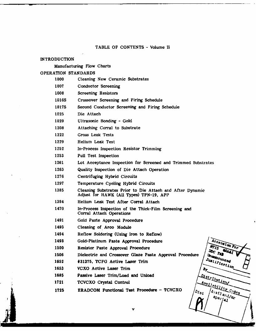
TABLE OF CONTENTS - Volume II
INTRODUCTION
Manufacturing Flow Charts
OPERATION STANDARDS1000 Cleaning New Ceramic Substrates
1007 Conductor Screening
1008 Screening Resistors
1016S Crossover Screening and Firing Schedule
1017S Second Conductor Screening and Firing Schedule
1025 Die Attach
1029 Ultrasonic Bonding - Gold
1208 Attaching Corral to Substrate
1222 Gross Leak Tests
1229 Helium Leak Test
1252 In-Process Inspection Resistor Trimming
1253 Pull Test Inspection
1261 Lot Acceptance Inspection for Screened and Trimmed Substrates
1263 Quality Inspection of Die Attach Operation
1276 Centrifuging Hybrid Circuits
1297 Temperature Cycling Hybrid Circuits
1385 Cleaning Substrates Prior to Die Attach arnd After DynamicAdjust for HAWK (All Types) TPN-19, APP
1394 Helium Leak Test After Corral Attach
1470 In-Process Inspection of the Thick-Film Screening andCorral Attach Operations
1491 Gold Paste Approval Procedure
1493 Cleaning of Arco Module
1494 Reflow Soldering (Using Iron to Reflow)
1498 Gold-Platinum Paste Approval Procedure Ac
1500 Resistor Paste Approval Procedure Zb
1506 Dielectric and Crossover Glaze Paste Approval Procedure e
1652 #31375, TCFG Active Laser Trim ~I ~w1653 VCXO Active Laser Trim
1685 Passive Laser Trim/Load and Unload
1721 TCVCXO Crystal Control
1725 ERADCOM Functional Test Procedure - TCVCXO /al
OPERATION STANDARDS (Continued)
1748 ERADCOM-TCFG Passive Trim Set-Up1755 Crystal Attach - Pre-Trim
1758 Potentiometer and Crystal Mounting
1759 TCFG - VCXO Marriage
1760 Potentiometer Assembly
1761 Burn-In Procedure for ERADCOM Modules H60388
1762 Inspection of ERADCOM Modules TCVCXO H60388
1763 TCVCXO Potting
1765 Procedure for Aging ERADCOM Modules
1766 Branding of TCVCXO
vi
vii
PART II
INTRODUCTION
Part II of the Final Report on the "ManLfacturing Methods and Technology
Engineering (MM&TE) Program for the Establishment of Production Techniques for
High-Density Thick-Film Circuits Used in Crystal Oscillators" includes manufacturing
flow charts, and detailed descriptions of all manufacturing, testing, and quality control
procedures employed in the production of the TCVCXO, ERADCOM Specification SCS 483.
While the device shares many of the standard procedures evolved at Raytheon-Quincy
for all types of thick-film hybrids, a large proportion of the processes and techniques
described in this section reflect the unique requirements of this application.
1 i
71771 717,.
ow. A fr
S7Eld AUYSa- ra.z'
S-S -A Aw* a SS 0, t0
zaw ~ ~ ~ ,W 0- Ae fla -Mtt.'dttt.,
rAOq S 1d.5 w
Awo. A ..o, (tnc
31102.1WA ~0'S fl R7
ex.: pCAi-,-1,' , 64%l-
rM01 Pt ws(rsx a ,e-0 .
ftir ~ AV67-1,4', W/fl J~ r ae . ~'
,ttflefPSS-flff /mern'') '-
Mm-,I i4.D Z -00 f z£SoiD-p 5dOCOor ,-n-,n -iWr 0, v
J'JD2-i A'4"Ooo e ''tA ..
,5.f CWc~m APEWrY Kr (ANFo .fwd A/lp"~ i-"
Cc~ ,Gww4'-t90m AAwow'WA. I-roo
o 4in247/Ev LA0 SEJAW4AII (I--
2~W# A~M V~, AarM'~ (,u.W Awasa
~YJ AWAWXV.PAM AV"WA
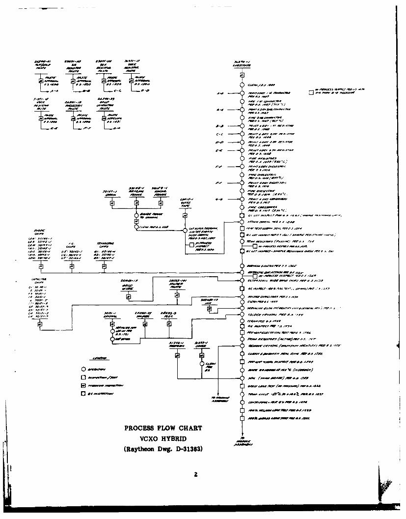
PROCESS FLOW CHART
VCXO HYBRID*F^r(Raytheon Dwg. D-31363)
4d~~~~f~~~4j -V,. ~ ild JP~jAw~x~w SIC AA ZwcJ,50
A-A W,, (, 4 r)
a-s, A. 10-r
os-roe T" -9A -'beso
L..,...- r II l
Pn-r7 LAC - 0~S~ .e.
)a'ie7-.3 52.t0w AVVAX ca,.,w- ~,~a~ ~o t-
At AV 0/6*
75a7aO'5 5'.e - 0.A
No-ro-O At a omAt
,~AtW.A -A
S'WflS4 4m ~ f, a.S S . Ottr
-m'W'Wo--fld ' -1 o W I~n
z~~AoocvoW)a-A.- pown.jcs -4C Me'nt-.>r., V
505 (,sqjW -med.s 7Mf
WAS ~ ~ ~ ~~ A 0..0r. asst~a a- S N
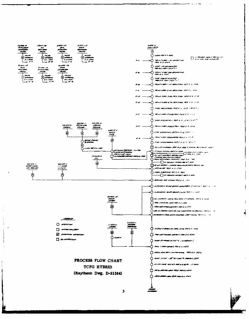
PROCESS FLOW CHART ~4XV
TCFG HYBRID(Raytheon Dwg. D-31364)
3-
-' cc . T 0 ... ... I .,.
...... o l WWS -
PROCESS FLOW CHART A..,,- ......
TCVCXO MODULE
, (Raytheon Dwg. D-31365)
i 4
Jam,-o a,9-
RAYTHEON C O PANY 1000
Foom 20-0044 1 Rev. 2
____ May 4, 1978
CLEANING NEW CERAMIC SUBSTRATES POC 78-6211
1.0 EQUIPMENT:
1.1 Ultrasonic cleaner, frequency 25 KC.
1.2 3000 ml. glass beakers
1.3 Drying oven (125*-1500 C)
1.4 Glass jar
1.5 Pyrex glass trays
1.6 Glass rod
2.0 MATERIALS:
2.1 Ceramic substrate
2.2 Trichloroethane (Degreaser Grade)
2.3 Acetone (Electronic grade)
2.4 Isopropanol (Electronic grade)
3.0 PROCEDURE:
3.1 Place ceramic substrates in a glass beaker to approximately500 ml. mark.
3.2 Cover the substrates with trichloroethane to approximately750 ml mark.
3.3 Clean in ultrasonic apparatus for 15 minutes. Using glassrod stir the substrates every 3-4 minutes.
3.4 Drain the trichloroethane and cover the substrates withAcetone.
3.5 Clean in ultrasonic apparatus for 5 minutes stirring
occasionally.
3.6 If the acetone becomes cloudy, drain it and repeat as in 3.5.
3.7 Drain the Acetone and cover the substrate with Isopropanol.
R A Y T H E 0 N C 0 M P A N Y 1000
F.- 20-0044 92
- e May 4, 1978
I &LEANING NEW CERAMIC SUBSTRATES POC 78-6211
3.0 PROCEDURE: Cont.
3.8 Clean in ultrasonic apparatus for 5 minutes stirringoccasionally.
3.9 Transfer the substrates into the glass tray and air dryfor 15 minutes. DO NOT HANDLE WITH BARE HANDS.
3.10 Place the tray with substrates in an oven at 125*-150'C for2 hours.
NOTE: Do not close the oven door completely for the first5 minutes the substrates are in the oven.
3.11 After drying, cool down the substrates to room temperatureand transfer them into clean glass jars. DO NOT HANDLE WITHBARE HANDS.
3.12 Mark the jar with the word "CLEANED, DATE, and TYPE ofsubstrate," and "DO NOT HANDLE SUBSTRATES WITH BARE HANDS.
R A Y T H E 0 N C 3 Al P A N YRAYTE Si-Aud 1007
. . . . . . ... . .S h e " I 1v 1 0Dee May 4, 1978
CONDUCTOR SCREENING POC 78-6211
1.0 PURPOSE:
This specification outlines the requirements to be met in printing conductorpatterns on to ceramic substrates.
2.0 SAFETY:
Avoid contact and inhalation of solvent and vapors from conductor paste.The use of gloves when cleaning with Axothane VG is recommended. Other-wise standard safety precautions should be observed.
3.0 APPLICABLE DOCUMENTS:
3.1 Operation Standards
3.1.1 Procedure for Adjusting Resistor and Conductor PasteViscosity O.S. 1048
3.1.2 Screener Set-Up O.S. loll
3.1.3 Firing Schedules - Furnace Profiles O.S. 1012
3.1.4 Adhesion Test O.S. 1022
3.1.5 Conductor Paste Approval O.S. 1491O.S. 1498O.S. 1501
3.1.6 Conductor Paste Control and Identification Procedure O.S. 1051
4.0 EQUIPMENT, TOOLING, GAUGES:
4.1 Equipment
4.1.1 Presco Screener4.1.2 Screens4.1.3 Conveyorized Drying Oven4.1.4 Firing Furnace4.1.5 Microscope 7.5 -30X magnification4.1.6 Clevite Brush Surfanalyzer Model 1504.1.7 Viscometer4.1.8 Heller Mixer
4.2 Tooling
4.2.1 Small tooling, gloves, finger cots, stainloss steel tweezers
i ~~~~~ ....... .L. ..L _1__10 8j i~ 8im
, R A Y T H F 0 N C 0 M P A N Y S, d 1007
.. . .2 fRev. 8
g May 4- 1Q7Rs CONDUCTOR SCREENING POC 78-6211
4.0 Cont.
4.3 Gages:
4.3.1 Nikon Comparator and charts
5.0 PROCESS REQUIREMENTS:
5.1 Material Requirements:
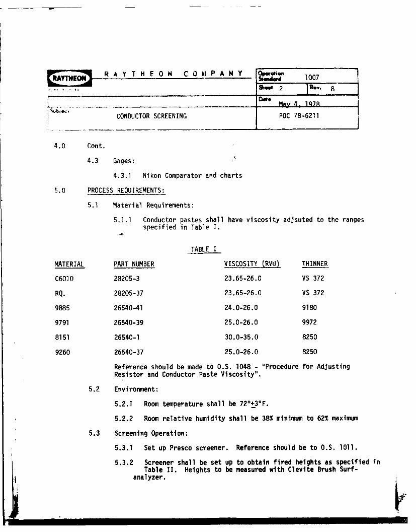
5.1.1 Conductor pastes shall have viscosity adjsuted to the rangesspecified in Table I.
TABLE I
MATERIAL PART NUMBER VISCOSITY (RVU) THINNER
C6010 28205-3 23.65-26.0 VS 372
RQ. 28205-37 23.65-26.0 VS 372
9885 26540-41 24.0-26.0 9180
9791 26540-39 25.0-26.0 9972
8151 26540-1 30.0-35.0 8250
9260 26540-37 25.0-26.0 8250
Reference should be made to O.S. 1048 - "Procedure for AdjustingResistor and Conductor Paste Viscosity".
5.2 Environment:
5.2.1 Room temperature shall be 72°+3°F.
5.2.2 Room relative humidity shall be 38% minimum to 62% maximum
5.3 Screening Operation:
5.3.1 Set up Presco screener. Reference should be to O.S. 1011.
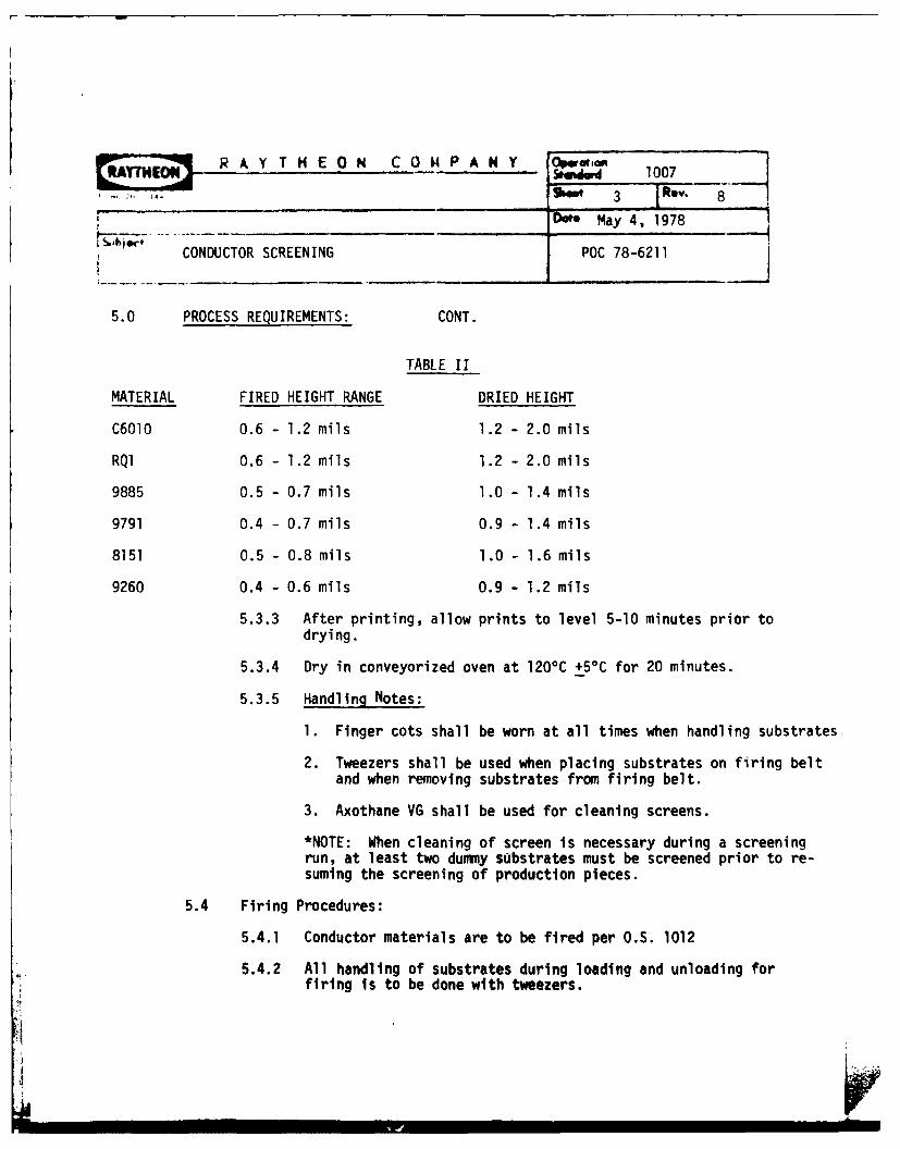
5.3.2 Screener shall be set up to obtain fired heights as specified inTable II. Heights to be measured with Clevite Brush Surf-
analyzer.
T R A Y T H E 0 N C 0 M P A N Y 1007Skw 3 _RIv 8
Dt' May 4, 1978
CONDUCTOR SCREENING POC 78-6211
5.0 PROCESS REQUIREMENTS: CONT.
TABLE II
MATERIAL FIRED HEIGHT RANGE DRIED HEIGHT
C6010 0.6 - 1.2 mils 1.2 - 2.0 mils
RQ1 0.6 - 1.2 mils 1.2 - 2.0 mils
9885 0.5 - 0.7 mils 1.0 - 1.4 mils
9791 0.4 - 0.7 mils 0.9 - 1.4 mils
8151 0.5 - 0.8 mils 1.0 - 1.6 mils
9260 0.4 - 0.6 mils 0.9 - 1.2 mils
5.3.3 After printing, allow prints to level 5-10 minutes prior todrying.
5.3.4 Dry in conveyorized oven at 1200C +50C for 20 minutes.
5.3.5 Handling Notes:
1. Finger cots shall be worn at all times when handling substrates
2. Tweezers shall be used when placing substrates on firing beltand when removing substrates from firing belt.
3. Axothane VG shall be used for cleaning screens.
*NOTE: When cleaning of screen is necessary during a screeningrun, at least two dummy substrates must be screened prior to re-suming the screening of production pieces.
5.4 Firing Procedures:
5.4.1 Conductor materials are to be fired per O.S. 1012
5.4.2 All handling of substrates during loading and unloading forfiring is to be done with tweezers.
II* I 1
R A Y T H E 0 H C 0 P A N Y .... ..... .
4 1 7"
- l~oMay 4, 1978
CONDUCTOR SCREENING POC 78-6211
6.0 PROCESS CONTROL:
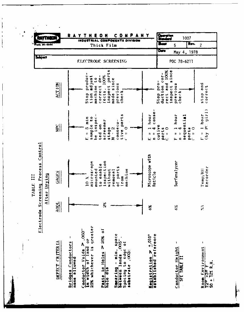
6.1 Control points as in Table III
6.2 Workmanship criteria as specified in O.S. 1265 shall apply toconductors screened onto substrates.
R.AY SYRIA EONPWY DIISIONY 1007
j_________________________________________Dee May 4, 1978
ELECTRODE SCREENING POC 78-6211
W 0 0~ Co 0.
E- - 0 0 0 .w 0
W) -40
E L. I I t. 1
otL. C- 3. tu
C~~ 4-0 0
0 0 a)
~~cc-4Q. 9
Ci) -.- cc
I. It w IIL
I[ATER A Y T H E 0 N C 0 4 P A N Y 0wr oM tdad 1008
F,....... . Sh w 1 1Rev.
_ Do* may 8, 1979
1subioctSCREENING RESISTORS POC 79-6390
1.0 PURPOSE:
This operation standard outlines the procedures to be followed for screeningand firing of resistor pastes.
2.0 SAFETY:
Contact and inhalation of solvent and vapors is to be avoided. Use ofgloves when cleaning with Axothane VG is recommended. Otherwise standardsafety precautions should be observed.
3.0 APPLICABLE DOCUMENTS:
3.1 Resistor Paste Approval O.S. 15003.2 Resistor Paste Blending Procedure O.S. 1036
3.3 Screener Set-Up O.S. 10213.4 Firing Profile, Characteristics, Use, and Frequencies O.S. 1012
4.0 EQUIPMENT, TOOLING, GAUGES:
4.1 Presco Screener4.2 Screens4.3 Microscope 7.5 - 30X magnification4.4 Conveyorized Drying Oven4.5 Firing Furnaces4.6 Clevite Brush Surfanalyzer Model 150
4.7 Small tooling, gloves, finger cots, stainless steel tweezers
5.0 ENVIRONMENT:
5.1 Room environment shall be maintained in accordance with O.S. 1507.
J 1 2 3 . ..... 5 ....
i . l 8 7 2 0 ......0 i J iz l
~~~R A Y T H E 0 N C 0 Mt P A 1N Y lO
2 ShRev.f ' ' 'Date
_ _ _June 27, 1978SCREENING RESISTORS POC 78-6365
6.0 PRODUCT REQUIREMENTS:
6.1 Resistor heights shall be within the limits of Table I.
TABLE I
RESISTOR TYPE DRIED HEIGHT FIRED HEIGHT
EMCA Firon 1.0 - 2.4 mils 0.6 - 1.2 mils
DuPont Birox 0.9 - 1.1 mils optimum 0.40 - 0.60 mils optimum
0.9 - 1.3 mils maximum 0.40 - 0.70 mils maximum
6.2 Screened resistors shall meet all workmanship criteria established
by O.S. 1265.
7.0 PROCESS REQUIREMENTS:
7.1 Set up screening machine per O.S. 1011.
7.2 Follow the Flow Chart I to determine the correct set-up and resistor
pastes to be used. The following guidelines should be used inscreening of resistor pastes.
7.2.1 After proper registration and best set-up are achieved, a
minimum of (ten(10) squeegee wipes should be made to "BreakIn" the screen, ink etc., before screening the samples.
7.2.2 When the screen is cleaned with Xothene, it is importantthat a minimum of (2) substrates be screened prior to screen-ing any samples or production substrates.
7.2.3 Allow screened resistors to level at room temperature for5-10 minutes prior to drying.
7.2.4 Resistors shall be dried in conveyor oven at 1200+50 fortwenty (20) minutes.
7.2.5 When firing resistor samples, simulate loaded kiln conditionsby placing 12" of ceramic substrates in front of and in backof samples.
7.2.6 No other materials (DielectricV, Conductors etc.) are to befired in resistor furnace during resistor firing.
Hil I il lm~~m V
RAY THEO_ N COMPANY OPeIrM =.. A HS d 1008
s h e t 3 R e . 2 j
Date May 8, 1979
______- SCREENING RESISTORS POC 79-6390
7.0 PROCESS REQUIREMENTS: Cont.
7.2.7 Tweezer handling of substrates is mandatory for loading and
off loading substrates from furnace. No substrate stackingis permitted. Handling without finger cots is forbidden atany time.
7.2.8 Sequence of screening resistors is optional if all resistors
are co-fired.
8.0 PROCESS CONTROL:
8.1 Screen operators monitor pattern fidelity (Registration, Voids, etc.)by checking at least (1) one substrate for every twenty-five (25)screened.
8.2 Monitor dried heights by taking one (1) substrate every 30 minutesfrom the drying belt. Record dry heights. Heights must be withinthe same limits established by the resistor paste tests.
8.3 Prior to any lot firing of resistors, a random sample from thescreened lot is to be fired. Resistors are to be read and recordedto determine that resistors are still within specified ranges. Aminimum of five (5) sample substrates ate to be so fired.
9.0 DOCUMENTATION:
Production inspection records shall be maintained for one year unlessprogram requirements dictate otherwise.
J!V
1_2 3 4
Resistor Paste Set-Up Screen asure driedScreening 4 samples eights from
Prep. Machine - eft and riqh-O.S.13de of substrat
5 6 7 8
Fire if heights Read and record If resistance Repeat sequencewithin spec. all resistance within spec., of steps 1-7
values screen lot. Mon, for each resis-itor dry ht. tor paste1 | sulstrate each
S30 minutes.
spec. rescreen out of spec. re- 1
until correctdry h. andthen fire refire samples
f resistancetill out ofec. blend paste
d resample
.9
Prio record If all resistan= Fr ofiring of resis- Read and record within spec. onFire lot Itors fire a ran- resistance -- o fire lot. If 3 substratesi
dom lOpc. sample more than 1 read 3 subtraesfrom screened lot ing out of spec. every 30 minute
Consult with Fore-man or engineerprior to lot Firing
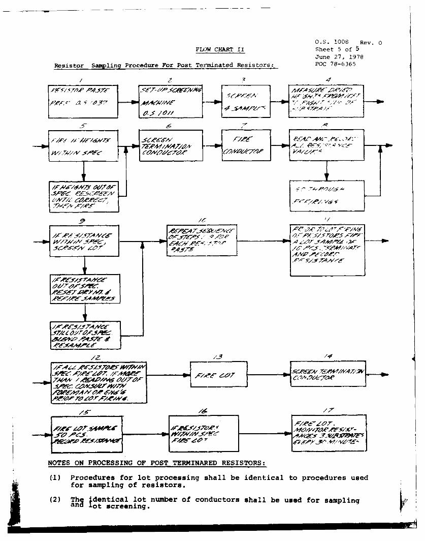
F: OW CHART I
RESISTOR SAMPLING PROCEDURE
O.C. 1008
Sh. 4 Rev. 0POC 78-6211
0.. 1008 Rev. 0
FUNW CHART II Sheet 5 of 5June 27, 1978
Resistor Sampling Procedure For Post Terminated Resistors: POC 78-6365
/ .4
F~r -, e4-ll-
72
t-oam -f -a
I'll'PRCSIG FPS ERIAE RSSOS(1)/ Prcdre o ltpocsig hl e dniclt poeursue
for sapin feisos
(2) Th dentica lo/ubeAfcodcor9hllb se o smln74and lo screening.OY7~
5,~ 6~AC~'Nome~
rRYHR A Y T H E 0 N C 0 M P A N Y 1016 S
Form20-044INDUSTRIAL COMPONENTS DIVISION
MICROELECTRONICS 1 of 2 I m 0
November 27, 1968subio CROSSOVER SCREENING AND FIRING SCHEDULE POC 68-9431
1.0 PURPOSE:
To specify a procedure for screening crossover glaze and to specifyfiring conditions.
2.0 SAFETY:
2.1 Avoid excessive contact and inhalation of solvent fumes.
2.2 Use caution near moving parts of the screener.
3.0 APPLICABLE DOCUMENTS:
3.1 Screener Setup Procedure - O.S.l0ll
3.2 Profiling Procedure - 0.S.1013
4.0 EQUIPMENT ,TOOLING AND GAUGES:
4.1 Air firing Furnace - Thick Film
4.2 Screener - Presco
4.3 Crossover Glaze - Dupont 8190 or equivalent
5.0 PRODUCT REQUIREMENT:
5.1 Crossover area must be free of holes as seen under 7X maqnificatori.
5.2 Crossover area must not exceed the specified dimension in theprint by more than .010" max. and must be no smaller in areathan indicated on the print.
5.3 The crossover must have a smooth, even appearance free of pitsand bumps as seen under 7X magnification.
6.0 PROCESS REQUIREMENTS:
6.1 Tweezer handling of substrates is required and finger cots shallbe used.
6.2 Room Temperature to be 72°F + 30 F.
6.3 Crossover is to be dried between 1000C - 1250 for 10-15 minutesof each application.
!0 0
Fo, 2k) 0044, 90 2 of 21RSV. 0I November 27, 1968
Subjec-t
CROSSOVER SCREENING AND FIRING SCHEDULE POC 68-9431
o.0 PROCESS REQUIREMENTS: (Continued)
6.4 Two coatings of crossover glaze are required as follows:
6.4.1 Screen the 1st layer
6.4.2 Dry
6.4.3 Fire as in 6.5
6.4.4 Screen the 2nd layer
6.4.5 Dry
6.4.6 Fire as in 6.5
6.5 Fire crossover glaze as follows:
6.5.1 Peak belt temperature of 8700C + 100C
6.5.2 (4-6) minutes soak at peak temperature.
7.0 PROCESS CONTROL:
7.1 Once an hour examine 10 piezes as per F5 Product Requirement.
8.0 QUALITY:
8.1 Process audit as per requirements in F5.
l~"YHR A Y T H E 0 N CO0M P ANY 1 017S
INDUSTRIAL COMPONENTS DIVISIONF.m o-0044 MICROELECTRONICS * of 2 ,
D** November 27, 1968subjec SECOND CONDUCTOR SCREENING AN[D FIRING
SCHEDULE POC 68-9427
1.0 PURPOSE:
To specity a procedure for screening and firing second conductorover crossover glaze.
2.0 SAFETY:
2.1 Avoid excessive contact and inhalation of solvent fumes.
2.2 Use caution near moving parts of the screener.
3.0 APPLICABLE DOCUMENTS:
3.1 Screener Setup Procedure - O.S.l01l
3.2 Profiling Procedure - 0.3.1013
3.3 Crossover screening and firing schedule - O.S.1016
4.0 EQUIPMENT, TOOLING & GAUGES:
4.1 Air firing furnace - Thick Film
4.2 Screener - Presco
4.3 Ohmmeter - Digital or equivalent
4.4 Conductor Paste - 7553 Dupont or C6010 Alloys Unlimited.
5.0 PRODUCT REQUIREMENTS:
5.1 Second conductor must be continuous and must contact andoverlap it's termination by .005" minimum.
5.2 The conductor width must be no less than 2/3 the specifiedwidth nor wider than .010" over the specified width.
5.3 The size of holes or indents must be such as not to reducethe width by more than 1/3.
5.4 The conductor should not appear to be sunk into the crossoverglaze in excess of requirements as in 5.2.
1 2,0 0
KmTnmmTT-TTT
rRhO RAYTHEON COMPANY e I0INDUSTRIAL COMPONENTS DIVISION NCO= 1017
Fo. 20-0044 9"Ot 2 o f 2 0 oD*November 27, 1918Subieet
SECOND CONDUCTOR SCREENING AND FIRING POC 68-9427SCI IEDULE
5.0 PRODUCT REQUIREMENTS: (Continued)
5.5 There shall be no shorting between the second conductor andthe conductor underneath as measured with a digital or othersuitable ohmmeter.
(,.0 PROCESS REQUIREMENTS:
6.1 Tweezer handling of substrates is required and finger cotsshall be used.
0.2 Room temperature to be 72 F + 30F.
,.3 Screen the second conductor to meet the requirements of F5.
,.4 Dry at 1000 - 1250 - 10-15 minutes.
t,.5 Fire in the 760 0C resistor firing furnace at a speed of 3"-,5"/min.
7.0 PROCESS CONTROL:
7.1 Once an hour examine and short check after timing to meet WS.
7.2 Once an hour perform a visual examination to meet requirementsof P5.1-P5.4 at screening before firing.
8.0 QUALITY:
8.1 Process audit as per requirements of F5.
RAYTHE N COM ANYl125
Fe.- 20-0044 s.,,1
D AT July 14, 1978
DIE ATTACH POC 78-6282_ 78-6410
1.0 PURPOSE:
To bond the die to the substrate or header by forming a goldsilicon eutectic.
2.0 SAFETY:
Use normal safety precautions in working near hot work fixtures.
3.0 EQUIPMENT AND TOOLING:
3.1 Die Attach Bonder: (K/S Model 607 or equivalent.)
3.2 Tweezers 3-C or equivalent
3.3 Heat Column Top Plate:
3.3.1 K & S - 601-14-0 (For TO-5 header) or equivalent3.3.2 K & S - 601-117-0 (For 1" X 1" substrate or equivalent3.3.3 K & S - 601-101-0 (For 1/2" X 1/2") or equivalent
3.4 Heat Collets: No. 5800 Titanium Carbide or equivalent
3.5 Mini heater No. 302 or equivalent
3.6 Nitrogen Atmosphere Storate Cabinet
3.7 Hot Plate - Thermolyne Model No. HPA1915B or equivalent
3.8 Mirrors No. 607-1-6 or equivalent
3.9 Mirror holder NO. 607-5V (with tray) or equivalent
3.10 Heater collet transforms No. 5037 or equivalent
3.11 Perforated (1" X 1/4 diamond holes) 1/32" thick aluminumplate 5 x 5 x 3/8 high.
4.0 MATERIAL AND SUPPLIES:
4.1 Hybrid Circuits
4.2 Chips on mirrors to be bonded.
1 2 3 1~ 4 5
i&hi1025I0-1" 0-0044 S e e 2 Re . 1.
________ August 7, 1 978
DIE ATTACH POC 78-62826410
5.0 PRODUCT REQUIREMENT:
5.1 O.S. 1265
6.0 PROCESS PROCEDURE:
6.1 All devices are to be die attached as follows, unless listedbelow. Heat column limits of 355 0C - 3650C and specificationlimits will be 350 0 C - 370 0C with a flow of nitrogen over unitto be bonded at the heat column surface. "For APP H60243 - LSIattach control limits to be 380 0 C - 390 0C and specificationlimits 375'C - 395°C."
6.2 Place the proper size die collet to be used in the machineand turn on Variac to approximately 9.0. Make sure that thecollet is being heated by just touching the side of the heateron the die collet.
6.3 After each collet chang, wait approximately 1-2 minutes forcollet to reach the temoerature of 400*C-5000C for controllimit and specification limit at 400°C-550°C before startingdie attach.NOTE: Vacuum must be in OFF position.
6.4 Place the units to be die attached on a hot plate. A maximumof ten units may be on the hot plate. Temperature for hotplate "Control Limits" .90*-210 ° and Specification-Limits1900 - 2500. For APP H60243 - Place a maximum of 5 (five)units on the preheat perforated plate sitting on the hot plate.Allow to heat there for a minimum of 3 (three) minutes. Remove1 (one) unit and place on hot plate for a minimum of 3 (three)minutes before transfering to heat columns.
6.5 Working from the hot plate place the unit on the heat columnand place under vacuum to hold the unit down. Pick up thesemiconductor chip to be attached making sure it fits square inthe die collet and the chip is in the right position per theAssembly Dwg. for the circuit being die attached.
6.6 Attach chip to substrate making sure you have good gold eutecticflow around chip by controlling the Mech. Vibrator of the diecollet and no eutectic balls around the chip.
4 i
~102-5
Fos"~ 20-0044
Doe--. &ec't .. UgUSt 7, 1978
DIE ATTACH POC 78-6282
6.0 PROCESS PROCEDURE: Cont.
6.7 Raise collet and remove the unit from the heat column. Placethe unit upside down on the carrying tray resting on the corral.For APP H60243 - Place the unit on the hot plate corral sideup for a minimum of 3 (three) minutes then place it on theperforated plate corral side up for a minimum of 3 (three)minutes and then place at angle on edge of an aluminum tray orflat on an aluminum foil covered fiber tray.
NOTE: For small substrates the hot plate can be eliminated.
7.0 REWORK:
7.1 Element Replacement for Hybrid and Multichip Microcircuits.Unless otherwise specified, replacement of attached elementsin hybrid and multichip microcircuits shall be permitted withthe following limitations:
7.2 Replacement of active or passive attached elements shall belimited to a maximum of 2 devices or 15 percent of the totalnumber of such elements in the microcircuit, whichever isgreater.
7.3 Regardless of the number of allowable element replacements, allreplacement of elements of the microcircuit must be accomplishedin no more than two recycles of any single microcircuit forrework.
8.0 INSPECTION:
8.1 See O.S. 1263
9.0 MAINTENANCE:
9.1 K & S #607-5, See Section 4 and also Section 2, "Adjustment"
9.2 Calibrate heat, column temperature each day.
9.3 Attach a thermocouple to a substrate in location where a diewould normally go.
9.4 Place substrate thermocouple assembly in place on heat columnand read millivolt output on glavonometer. Use chart to convertto degrees.
9.5 Correct temperature by raising or lowering heat control.
P -om 4 jfts 0"
August 8, 1978
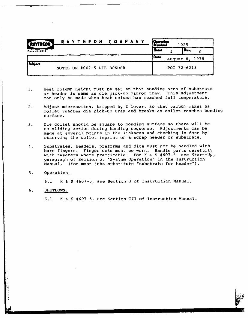
NOTES ON #607-5 DIE BONDER POC 72-6213
1. Heat column height must be set so that bonding area of substrateor header is same as die pick-up mirror tray. This adjustmentcan only be made when heat column has reached full temperature.
2. Adjust microswitch, tripped by Z lever, so that vacuum makes ascollet reaches die pick-up tray and breaks as collet reaches bondingsurface.
3. Die collet should be square to bonding surface so there will beno sliding action during bonding sequence. Adjustments can bemade at several points in the linkages and checking is done byobserving the collet imprint on a scrap header or substrate.
4. Substrates, headers, preforms and dice must not be handled withbare fingers. Finger cots must be worn. Handle parts carefullywith tweezers where practicable. For K & S #607-5 see Start-Up,paragraph of Section 3, "System Operation" in the InstructionManual. (For most jobs substitute "substrate for header").
5. Operation
6.1 K & S #607-5, see Section 3 of Instruction Manual.
6. SHUTDOWN:
6.1 K & S #607-5, see Section III of Instruction Manual.
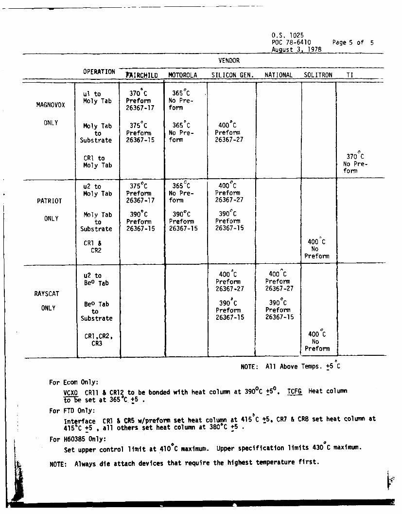
O.S. 1025POC 78-6410 Page 5 of 5August 3, 1978
VENDOR
OPERATION PAIRCHILD MOTOROLA SILICON GEN. NATIONAL SOLITRON TI
ul to 370 C 365&C
MAGNOVOX Moly Tab Preform No Pre-26367-17 form
ONLY Moly Tab 375 0C 365 C 400 C
to Preform No Pre- PreformSubstrate 26367-15 form 26367-27
CR1 to 370 CMoly Tab No Pre-
form
u2 to 375 0C 365CC 400 CMoly Tab Preform No Pre- Preform
PATRIOT 26367-17 form 26367-27
ONLY Moly Tab 3900C 3900C 3900 Cto Preform Preform Preform
Substrate 26367-15 26367-15 26367-15
CRI & 400 CCR2 No
Preform
u2 to 400 C 400 CBeO Tab Preform Preform
RAYSCAT 26367-27 26367-27
ONLY BeO Tab 390 C 3900Cto Preform Preform
Substrate 26367-15 26367-15
CR1 ,CR2, 400 CCR3 No
_ _Preform
NOTE: All Above Temps. +5 C
For Ecom Only:
VCXO CR11 & CR12 to be bonded with heat column at 390°C +5°. TCFG Heat column
tobe set at 3650C,+5
For FTD Only:
Interface CR1 & CR5 w/preform set heat column at 415 C +5, CR7 & CR8 set heat column at4156C +5 , all others set heat column at 3806C +5
For H60385 Only:
Set upper control limit at 410 C maximum. Upper specification limits 430 C maximum.
NOTE: Always die attach devices that require the highest temperature first.
m II I m IV
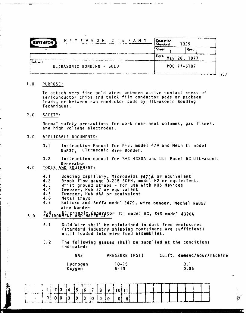
RA Y T H E 0 N C , A N Y 0waion-L- S 5indard 1029
Shot 1 ]Rev.
, , ....... .... .... ... May 26, 1977Subject ULTRASONIC BONDING - GOLD POC 77-6187
1.0 PURPOSE:
To attach very fine gold wires between active contact areas ofsemiconductor chips and thick film conductor pads or packageleads, or between two conductor pads by Ultrasonic BondingTechniques.
2.0 SAFETY:
Normal safety precautions for work near heat columns, gas flames,and high voltage electrodes.
3.0 APPLICABLE DOCUMENTS:
3.1 Instruction Manual for K+S, model 479 and Mech EL model
Nu837, Ultrasonic Wire Bonder.
3.2 Instruction manual for K+S 4320A and Uti Model 5C UltrasonicGenerator
4.0 TOOLS AND EQUIPMENT:
4.1 Bonding Capillary, Microswiss #'472A or equivalent4.2 Brook flow gauge 0-225 SCFH, model H2 or equivalent.4.3 Wrist ground straps - for use with MOS devices4.4 Tweezer, Hub #7 or equivalent4.5 Tweezer, Hub #AA or equivalent4.6 Metal trays4.7 Kulicke and Soffa model 2479, wire bonder, Mechel Nu827
wire bonder4.8 UltfaAka . tor Uti model 5C, K+S model 4320A
5.0 ENVIRONMEN
5.1 Gold 'wire shall be maintained in dust free enclosures(standard industry shipping containers are sufficient)until loaded into wire feed assemblies.
5.2 The following gasses shall be supplied at the conditionsindicated:
GAS PRESSURE (PSi) cu.ft. demand/hour/machine
Hydrogen 10-15 0.1Oxygen 5-10 0.05
1 .... 21 4 5 6 7 8 9 10 1
.010 0 LIIIIIII I
A N Y at I on
2 0~Do te.............. May 26. 1977
ULTRASONIC BONDING - GOLD POC 77-6187
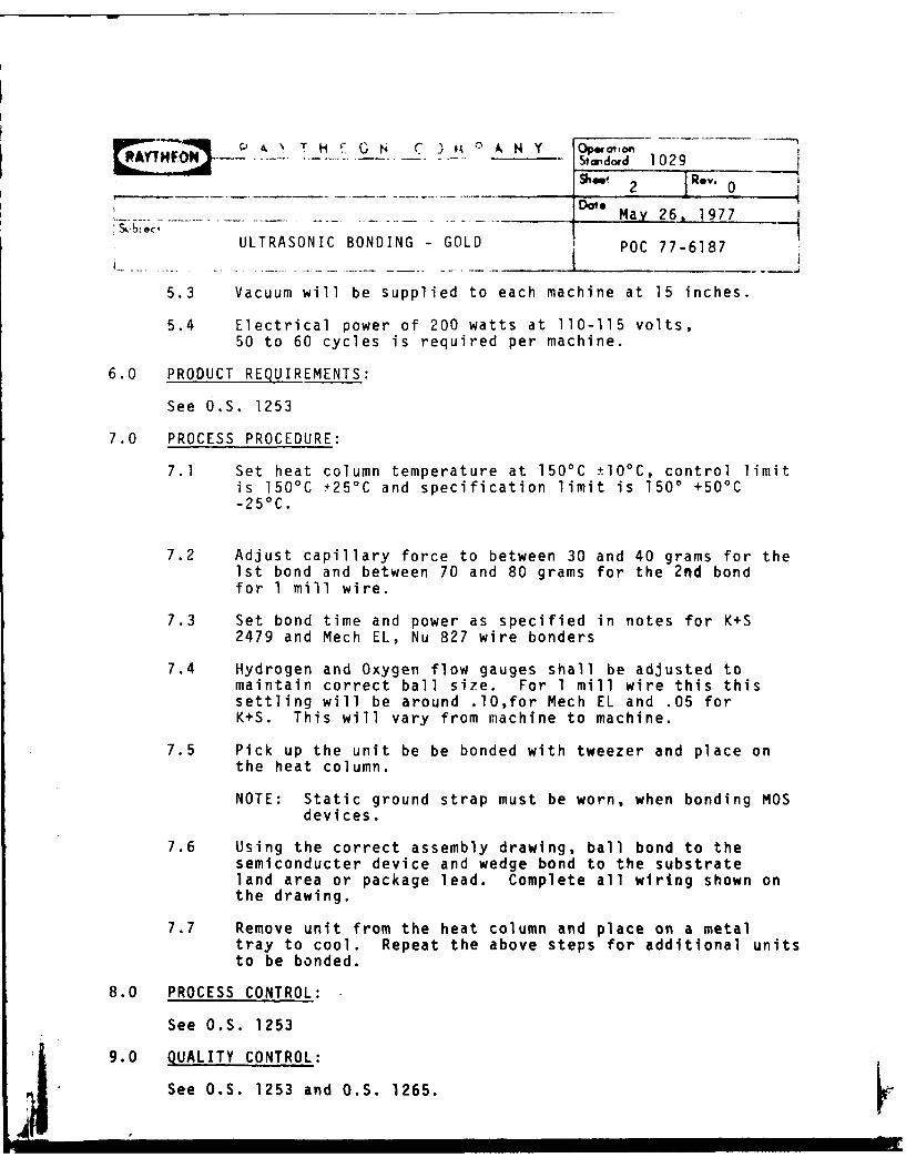
5.3 Vacuum will be supplied to each machine at 15 inches.
5.4 Electrical power of 200 watts at 110-115 volts,50 to 60 cycles is required per machine.
6.0 PRODUCT REQUIREMENTS:
See O.S. 1253
7.0 PROCESS PROCEDURE:
7.1 Set heat column temperature at 150'C ±10C, control limitis 150'C ±25°C and specification limit is 1500 +500 C-25°C.
7.2 Adjust capillary force to between 30 and 40 grams for the1st bond and between 70 and 80 grams for the 2nd bondfor 1 mill wire.
7.3 Set bond time and power as specified in notes for K+S2479 and Mech EL, Nu 827 wire bonders
7.4 Hydrogen and Oxygen flow gauges shall be adjusted tomaintain correct ball si7e. For 1 mill wire this thissettling will be around .l0,for Mech EL and .05 forK+S. This will vary from machine to machine.
7.5 Pick up the unit be be bonded with tweezer and place onthe heat column.
NOTE: Static ground strap must be worn, when bonding MOSdevices.
7.6 Using the correct assembly drawing, ball bond to thesemiconducter device and wedge bond to the substrateland area or package lead. Complete all wiring shown onthe drawing.
7.7 Remove unit from the heat column and place on a metaltray to cool. Repeat the above steps for additional unitsto be bonded.
8.0 PROCESS CONTROL:
See O.S. 1253
9.0 QUALITY CONTROL:
See O.S. 1253 and O.S. 1265.
R Y T H i ON C) M A N Y Operaio"... ... .... a.dord 1029
3 InDot* May 26, 1977
NOTES ON MECH EL NU827 WIRE BONDERPOC 77-6187
1.0 Flame Off
1.1 Ball size generally should be twice wire size.
1.2 Hydrogen flow generally set at .10 on flow meter,using a 5002-2 torch
1.3 Ball size is controlled by:
a) Hydrogen flow (flame size)b) Torch speedc) Position of torch to wired) tail length
2.0 Equipment Set Up and Adjustment
2.1 Heat column should be adjusted so that capillary is levelwith work. An imprint of the capillary with a ballshould give a perfect circle on a gold conductor.
2.2 Bond pressure for .001 wire should be 1st bond 30 to40 grams, 2nd bond 70-80.
2.3 Capillary should be installed flush with top of trans-ducer, using a new set screw.
2.4 Tune Uti generator to low point. Tune Mech-EL genera-tor to high point.
2.5 Set time to 3.0 on Uti generator. Set time to 5.0 onMech EL generator.
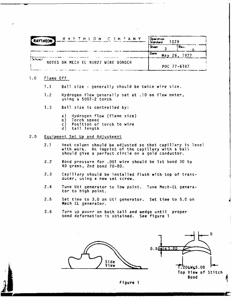
2.6 Turn up power on both ball and wedge until properbond deformation is obtained. See figure 1
SideView O
i2 D SW!65.0
Top View of Stitch
Bond
Figure 1
R A I H E 0 'A C 3 tiP A N Y Operation"ENStandard 1029
-- -. ___Shoo~ Rev.4 0
- -- ot May 26, 1977.. ... ....- --- 4
NOTES ON MECH EL NU827 WIRE BONDER POC 77-6187
3.0 Equipment Operation
3.1 Start - up
a) Turn on power; machine, Ultrasonic Generator, heatcolumn heaters.
b) Open hydrogen valve full (size of the .002" Orificetorch restricts flow to proper amount) light torch.
c) Tune generator; Uti to a minimum , Mech-EL to amaximum.
d) Cycle machine a few times to get machine in propersequence.
e) Practice bond on a piece of scrap to be sure machineis cycling properly.
3.2 Operation
a) Machine at reset - ball at end of wireb) Lower Z-arm until ball at the end of the capillary
contacts semiconductor chip.c) Continue lowering Z-arm until ultrasonics fire and bond
is made.d) Raise Z-arm until capillary lifts off semiconductor
chip, machine cycles to second bond, L.E.D. lights.e) Loop wire, then lower Z-arm until capillary and wire
contact second bond land surface.f) Continue lowering Z-arm until ultrasonics fire and bond
is made. Clamps will close when bond is complete.g) Raise z-arm; capillary lifts off, tail forms,
and wire breaks. Continue raising Z-arm until flameoff activates and sweeps past the tail and forms a newball, then clamps open.
h) Machine now at reset, ready for next bond.
3.3 Shut Down
a) Be sure work is removed from work holder.b) Blow out Hydrogen torch.c) Turn off Hydrogend) Turn off heaters, Ultrasonic Generator and machine
power.
4.0 Trouble Shooting
4.1 Won't bond
a) Check temperature of work holder, (raise temp. if possible)b i Check work holder heightc Check for proper Instalation of capillaryd) Check tune of generator
L--lue
/
I
k T~ H EO0N A ?i.AN Y OperationStandard 1029 -
CDate May 26, 1977
NOTES ON MECH EL NU827 WIRE BONDERPOC 77-6187
e) Check to see that generator fired when capillarycontacts work.
f) Check force on capillaryg) Turn up Ultrasonic power until wire bonds.
4.2 Inconsi--tant ball size
4.2.1 Due to varying wire tail length.
a) Check action of wire clamp after.second bond.
1. clamps close on wire2. clamps pivot downward3. raise Z-arm untill torch flames
across wire4. clamps open5. clamps pivot upward
b) Check that clamps close right on wire.c) Check that clamp pivot bearing is tight.d) Check that clamp stop is tight.
4.2.2 Flame Misadjusted
a) Check that flame off torch dnd flame do notcontact work
b) Check that flame passes by the capillary.c) Check that torch is not binding on its bear-
ing or is to loose.d) Check that Hydrogen hose is not jamming be-
tween flame off arm, and chasis.e) Check that torch position has not slipped
up or down, in or out. The flame mustcontact the tail.
f) Check that the flame is unrestricted, andcone shapped.
4.2.3 Machine cycling properly
a) Clamps remain closed while torch passes tail.b) Flame off operating only after second bond.
R A)Y TH CN C :'A NY OionLRYMa* -- otp'n d1029.
_6 Ro 0
Dte May 26. 1977i b,e
NOTES ON MECK EL NU827 WIRE BONDER POC 77-6187.
4.3 Tailing (wire not breaking at second bond but half wayup the wire)
a) Check capillary for wearb) Check temperature (lower if possible)c) Check forced) Turn time down and Ultrasonic power upe) Replace capillary with a small inside cone capillary,,
"Small Precision" part no. U+S-17S or equivalent.
4.4 Wire not breaking after second bond, lifting second bond.
a) Check capillary for wearb) Check temperature (raise if possible)c) Check forced) Lower force and raise Ultrasonic power
4.5 Ball size too small or large
a) Check hydrogen flowb) Turn tail adjust for proper size. Reduce tail
length if ball size to large. Increase tail lengthif ball size to small.
5.0 Maintainance
5.1 Lubricate bearings and bushings on all moving partsmonthly.
5.2 Check all hoses for wear.
5.3 Check all exposed wiring for wear.
5.4 Check ground daily.
y 0N C AA 'N Y r0p al on--- _____ Stwidrd 1029
_t 7 0
--- May 26, 1977
NOTES ON K+S 2479 WIRE BONDER POC 77-6187
1.0 Flame off
1.1 Ball size - generally should be twice wire size.
1.2 Hydrogen flow generally set at .05 on flow meter usinga 5004-5 torch.
1.3 Oxygen flow generally set at .025 on flow meter usinga 5004-3 torch.
1.4 Ball siLe is controlled bya) Hydrogen oxygen flow (flame size)b) Hydrogen oxygen flame mixture (flame sharpness)c) Position of torch to wired) Tail length
2.0 Equipment set up and adjustment
2.1 Heat column should be adjusted so that capillary islevel with work. An imprint of the capillary without aa ball should give a perfect circle on a gold conductor.
2.2 Bond pressure for .001 wire should be 1st bond 30 to 40grams, 2nd bond 70-80 grams.
2.3 Capillary should be installed using a K+S gauge blockmarked 472 as shown, using a new set screw
TransducerStScrew
4Capillary Height FixtureCapillary
2.4 Push test button on generator for 5 seconds to tunegenerator, a deflection on the meter should be observed.
2.5 Install a new spool of wire. Start the wire from thered end of the spool. Feed the wire through the hole underthe spool holder, between the glass slider, over the spring
tensioner, through the guide ring, through the clamp guide,through the clamp, thread the capillary pushing the testswitch if necessary.
i 0 N Oip-;AN Yon....... da 1029
. ...... ....... Date
May 26, 1977
NOTES ON K+S 2479 WIRE BONDER POC 77-6187
2.6 Open Hydrogen valve to .05, open Oxygen valve to .025.
2.7 Light flame with lighter
2.8 Cycle machine to flame off excess wire
2.9 Adjust Hydroqen and Oxygen flow until proper ball sizeis obtained.
2.10 Set time to between 1.0 and 2.0.
2.11 Turn up power on both ball and wedge until proper bonddeformation is obtained. See Figure 1 in notes on Mech ElNu 827 Wire bonder.
3.0 Equipment operation
3.1 Start - up
a) Turn on power: machine, Ultrasonic generator and lightsb) Open hydrogen flow valve to .05, open oxygen flow
valve to .025. Light torch usinq lighter.c) Push test switch to tune generator.
3.2 Operation in search mode
a) Depress the Mode switch to the 479 position.b) Place a module in the work holder.c) Using the spot light target over the first chip pad to
be bonded.d) Depress the chessman button to cycle the machine to
first search position.e) Adjust the search height using the left hand lever.f) Correct any errors in targeting and release button.
The ball will bond and the machine will cycle to loopposition.
g) Correct any miss-alignment in the spot light byturning the brass adjusting screws on the spotlight assy.
h) Using the spot light target over the correct land forsecond bond.
i) Depress the chessman button to cycle the machine tosecond search.
j) Adjust the search height using the right hand lever.k) Correct any error in targetting and release the button.
The stitch will bond, the wire will break and the flameoff torch will sweep across the raised capillary toform the ball for the next bond.
__O St' adad 1029S et 9 Rev. 0
'DateS.... . .. . .y 26, 1977
NOTES ON K+S 2479 WIRE BONDER POC 77-6187
3.3 Operation in Hybrid mode
a) Switch mode switch to the Hybrid positionb) Place a module in the work holderc) Using the spotlight target over the first chip pad
to be bonded.d) Depress the Z-arm, the clamps will open and the machine
will cycle to the first bond mode.e) Continue to depress the Z-arm untill the ball contacts
the first chip bond pad. Continue depressing theZ-arm until the Ultrasonics fire and the ball isbonded to the chip.
f) Raise the Z-arm to the top of the stroke to cycle themachine to the second bond mode. (Note: failure torelease the Z-arm to the top of the stroke willresult in the machine not cycling to the second bondmode and the machine will not bond coorectly duringthe following steps).
g) Target over the correct land to be bondedh) Depress the Z-arm until the capillary and wire contact
the land. Continue depressing the Z-arm until theUltrasonics fire and the bond is made
i) Raise the Z-arm to the top of the stroke. The clampswill close on the wire and pull up, breaking the wireoff at the second bond. The flame off torch willsweep by the capillary, cut the wire and form the ball.The remaining tail will go down the vacuum tube.The machine is now in reset position.
4.0 Trouble Shooting
4.1 Won't bond
a) Check temperature of the work holder (raise temp.if possible)
b) Check work holder heightc) Check for proper instation of the capillary.d) Push test button, check for deflection of the needle
on the tune meter.e) Check to see that the generator fires when the capillary
contacts work. Adjust the micro switch if necessary.f) Check the force on the capillary, adjust if necessary.g) Check time setting between 1.0 and 2.0 for .001 wire.h) Turn up Ultrasonic power until the wire bonds.
R FA Y T HF P A NY Op0to______!E 102910 1
€. _ _o May 26, 1977
NOTES ON K+S 2479 WIRE BONDER POC 77-6187
4.2 Inconsistant ball size, search mode
4.2.1 Due to varying wire tail length
a) Check clamps closing tightlyb) Check that clamp assy is tightc) Check that there is no foreign material in
the clamp jaws.d) Check clamp actions:
1. switch machine to set up mode2. manually turn the drive pulley and
belt to cycle the machine3. reset position clamps closed4. as capillary goes down to the work,
the clamp opens5. clamp stays open through; first bond,
loop, second bond.6. clamp closes after second bond7. capillary moves up leaving a short
tail8. clamp assy moves up breaking the wire9. torch flames off the tail forming the
ball, machine is now back in resetposition.
4.2.2 Inconsistant ball size due to flame torch
a) rhpck pressure at the oxygen and hydrogen tanks
c) Check flow rate of oxygen and hydrogend) Direct illuminator light away from work. Manu-
ally move flame to wire. Check shape of theflame and psoition of flame with respect to thewire and capillary. The tip of the hot partof the flame should be contacting the wire.
___ _ Capilary
1/16"
TORCH
H --a i re
inno Par ofllame"
_I H E 0 N C 0 P A N Y Opera,-~H0N-- Se.fa 1029S h o t 1 1 R - . 0
Dte May 26, 1977
-bi act
NOTES ON K+S 2479 WIRE BONDER POC 77-6187
e) In the set up mode, manually cycle the machine tothe flame off cycle. Check that the torch passesthe wire by about 1/16 inch. Adjust linkage ifnecessary.
f) After all position and linkage adjustments havebeen made, fine adjustment of the hydrogen andoxygen can be made to get correct ball size.NOTE 1: If the flow rates are changed the positionof the flame may change, creating the need for torchposition to be readjusted.NOTE 2: Increasing the hydrogen will make the balllarger, decreasing hydrogen will make the ballsmaller. Increasing the oxygen will make the ballsmaller, decreasing oxygen will make the balllarger.
4.3 Tailing (wire not breaking at second bond, but half wayup the wire)
a) Check capillary for wearb) Check temperature (lower if possible)c) Check forced) Turn time down and Ultrasonic power upe) ReDIA-- caDillary with a small inside cone, capillary
"Small Precision" part no. U+S-17S or equivalent.
4.4 Wire not breaking after second bond, lifting the secondbond.
a) Check capillary for wearb) Check temperature (raise if possible)c Check force
Lower force and raise Ultrasonic power.
4.5 Shut down
a) Remove all work from work holderb) Blow out hydrogen torchc) Turn of hydrogen and oxygend) Turn off heaters, Ultrasonic generator lights and mach-
ine power.
5.0 Maintanence
C1.1 Lubricate bearings and bushings on all moving parts.
5.2 Check all hoses for wear
j 5.3 Check all exposed wiring for wear
5.4 Check ground daily
V .Y'&H E 0 C M A N Y OWIfRAY-- G"4r4 1208
. ... ,m 1 7v
D4__ Jan. 26, 1978
POC 78-6033i ATTACHING CORRAL TO SUBSTRATE
1.0 PURPOSE:
This document outlines the requirements and process for assemblingthe corral to the substrate, in the Raytheor "Pin-Pak" during thesecond glaze firing cycle.
2.0 SAFETY:
observe normal safety precautions.
3.0 APPLICABLE DOCUMENTS:
3.1 Firing Schedules - Furnace Profiles - O.S. 1012
3.2 O.S. 1207
4.0 EQUIPMENT, TOOLING, GAGES:
4.1 Furnace BTU - 3 zone set fur glaze profile.
4.2 Furnace Settings - @520 0 -540 0 C, 3 i/2"/min. belt speed.
4.3 Fixtures - CMD00105-144 and CMD00105-199.
5.0 PRODUCT REQUIREMENTS:
5.1 Corral and substrate assembly must exhibit a tight seal of1 X 10-8 std.-cc. Helium/sec. on a Veeco check.
5.2 Visual and Dimensional Inspection of Corral/Substrate Assembly.per O.S. 1265.
6.0 PROCESS REQUIREMENTS:
6.1 Pre-Operation Procedure;
6.1.1 Corrals will have presintered glass on one face perO.S. 1127 and O.S. 1207.
6.1.2 Substrates will have been cleaned per O.S. 1043.
1 A 2 3 : *1 *7 O 5 4 •.' L ' ,
- itQ10C1M'ANY 0Pwaiav
'" .... ... gre Jan. 26, 1978
POC 78-6033ATTACHING CORRAL TO SUBSTRATE
6.0 PROCESS REQUIREMENTS:
6.1 Pre-Operation Procedure: Cont.
6.1.3 Burnish lightly with fiberglass brush. Clean per O.S.1043
Note: Type H60171A substrates which have been laser trimmeddo not require burnishing prior to corral attach.
6.1.4 A sufficient number of fixtures will be on hand.
6.1.5 Clean burned in glass off fixtures once per week,using a wire brush.
tA M R A Y T H E 0 N C 0 M P A N Y Ortion 1208
e20-0044 2 Rev. 5
or 0-0Dec.23, 1974
SubjectATTACHING CORRAL TO SUBSTRATE POC 74-6347
6.0 PROCESS REQUIREMENTS: Cont.
6.2 Operation Procedure:
6.2.1 Place substrate, circuit side up, in fixture, takingcare that it seats within pins.
6.2.2 Place cover plate on fixture.
6.2.3 Place corral, glass side down, into recess in coverplate, making certain that it drops down flat ontosubstrate.
6.2.4 Place weight on top of corral in fixture.
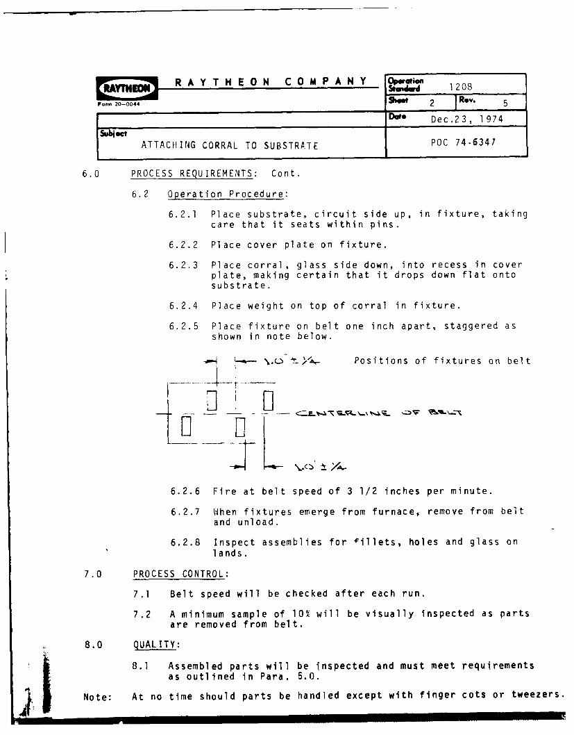
6.2.5 Place fixture on belt one inch apart, staggered asshown in note below.
-- c._ 4.%> _ Positions of fixtures on belt
6.2.6 Fire at belt speed of 3 1/2 inches per minute.
6.2.7 When fixtures emerge from furnace, remove from beltand unload.
6.2.8 Inspect assemblies for fillets, holes and glass onlands.
7.0 PROCESS CONTROL:
7.1 Belt speed will be checked after each run.
7.2 A minimum sample of 10% will be visually inspected as partsare removed from belt.
8.0 QUALITY:
8.1 Assembled parts will be inspected and must meet requirementsas outlined in Para. 5.0.I Note: At no time should parts be handled except with finger cots or tweezers.
R A Y T H E 0 N C 0 M P A N Y 1o
INDUSTRIAL COMPONENTS DIVISION 1208Form 20-00443 4
Jan. 14, 1976
ATTACHING CORRAL TO SUBSTRATE PO( 75-63424,,
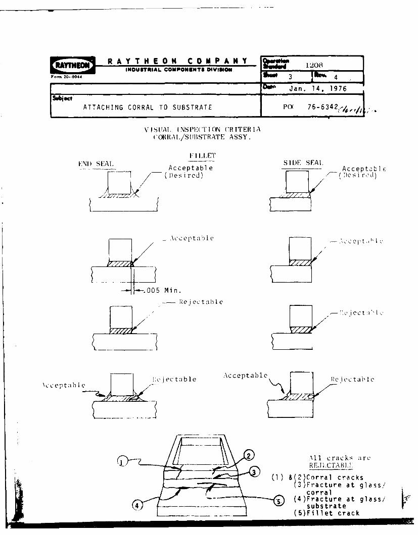
VISUAl, INSPE(ITION CRITERIACOIRAI,/SIIBSTRATE ASSY.
F 1 1,LETEIND SEAL. SIDE SEAl.
_-(Acceptable AcceptablD )es i red) / Des irod)
Acceptable e ) t
--005 Min.
Re j ec t able
!*cjectable A\cceptable Re iectai'lo\ccep'tah I c
Al1 cracks arc_ REd 1C"ABIA.
-~ (1) &(2)Corral cracks(3)Fracture at glass,
corral
(4)Fracture at glass/substrate
(5)Fillet crack
, R A Y T H E 0 N C. 0 10 P A N Y OperatioRAWs.. 1222
..... , o,,,,Show l ,. 21 R". 29
Date April 5, 1980
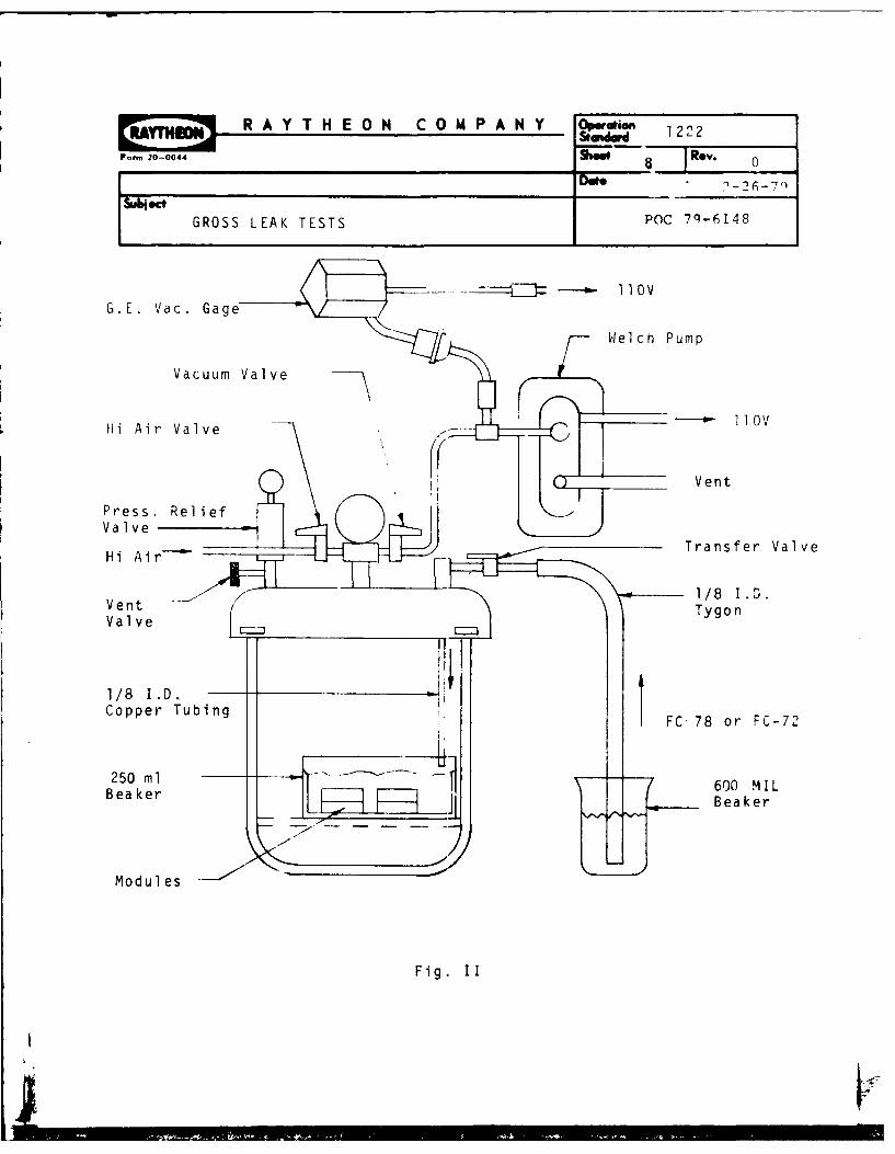
Subg ctI GROSS LEAK TESTS POC 80-4 300
J}41.0 PURPOSE:
1.1 To specify a method of Gross Leak Testing hermetically sealed hybrid
circuits using fluorochem FC78, FC-72, FC-48 or FC-40.
2.0 SAFETY:
2.1 Normal precautions are to be observed for handling solutions.
3.0 EQUIPMENT AND TOOLS:
3.1 Pressure/vacuum Bomb Tank 0-100 PSI and capable of less than 1 Torr.
3.2 Leak test station agnstromics Model #1501 or equivalent.
3.3 Oven 0-200'C.
3.4 Tweezer or holding fixture.
3.5 Welch Pump or equivalent
3.6 G.E. Vacuum gage or equivalent
4.0 MATERIAL AND SUPPLIES:
4.1 FC-78 or FC-72 Fluorocarbon
4.2 FC-40 or FC-48 Fluorocarbon
4.3 Whatman #50 Filter paper or equivalent
5.0 REQUIREMENTS:
5.1 No bubble comes from package under test.
6.0 PROCEDURE: For pressure testing only. (No vacuum applied)
6.1 Place packages to be tested in a beaker and cover with FC-78 or FC-72.
NOTE: Filter FC-78 or FC-72 each time before using.
6.2 Place in the pressure bomb tank and seal, and place under pressureand time as specified in Table I.
,4.1_, 2.. 4 5 6 | 7 ;8 -4 -'i29. 1 1 .1 6 10
I29I t[7 lL t ,_ll] lll l ~ l
~~R A Y T H E 0 N C 0 M P A N Y Opwln 22
RP 1222
Form~ 20-0044 9 0 2 e. 1
DON Feb. 26, 197q
GROSS LEAK TESTS POC 70-6148
6.0 Cont.
6.3 Remove the pressure from the tank, and remove the pack~age.
6.4 Pour off the FC-78 dr FC-72 tito & ldean container.
6.5 Allow the packages to dry for 3 minutes.
E.6 Filter the FC-40 or FC-48 before using each time.
6 7 Place FC-40 or FC-48 in the leak test station and set the ter:ner-ature at 125°C + 5oC.
6 8 Place the package to be tested in the FC-40 or FC-48 at adepth of 2 inches below the surface for 30 seconds.
6.9 Look for bubbles or streams of bubble: coming from the packaqe.If bubbles are observed the package is to be rejected. If nobubbles are observed the package is acceptable.
6 10 Remove from the FC-40 and dry for 5 minutes
7.0 PROCEDURE: For vacuum/pressure (Refer Fig. 2) preconditioning.Per MIL-STD-883B, Method 1014.2 Test Condition C.
Note: Binks tank with vacuum fittings should be used. Technicianshould pre-set the reduction valve to deliver the applicablepressure for the pressure application phase of this test.
7.1 Place packages to be tested in a 2rO mililiter graduated beaker.Note height of packages in beaker.
7.2 Shut off all tank cover valves.
7.3 Place beaker in tank so that the FC-78 or PC-62 copper Inlettube wilT be pdsitiened in te beaker -*1ver the oover is closed.
7.4 Seal the tank.
7.5 Pour approximately 300 ml FC-78 or FCq72 into a 600 mlgraduated beaker.
7.6 Start vacuum pump.
7.7 Place the FC-78 or FC-72 4nl6ttbbe Attlched to one of thecover valvbs in'the 600 ml FC6'S'8oV'FQ?2"reservoir beaker.
R A Y " H E 0 N C 0 M P A NY kudw 1222
114 149" 3 77 . 5
'Fte Feb. 26, 1979
subiect_ _ 7 ___1
GRCSS LEAK TESTS pnr 7q-6148
7.0 PROCEDURE: Cont.
7.8 Open cover valve attached to vacuum line. Shut off valve aftervacuum in tank is below 1,000 microns (1 torr). Allow tank toremain at 5 Torr vacuum or lower for 1 hour.
7.9 Cpen FC-78 or FC-72 inlet valve very slowly and allow FC-78 orFC-72 to enter the tank. Entry rate should be between 50 mland 200 ml per minute. The total amount to be delivered to thetank should be pre-determined dependinq on the height of thepackages within the tank. A quantity of FC-78 or T' -72 inaddition to the calculated quantity should be delivered to thetank. This additional quantity should be about 50 millilitersand is necessary due to evaporation resulting from the appliedvacuum.
7.10 Close FC-78 or FC-72 inlet valve after the appropriate amounthas been delivered.
7.11 Relieve vacuum by opening vent valve.
7.12 Close pressure vent by valve.
7.13 Open Hi Pressure valve and allow tank to attain the speciviedpressure. (See Table I).
7.14 Hold chamber under this pressure for the specified time.(See Table I).
7.15 At the end of this time, the pressure shall be released andthe devices removed from the pressure chamber.
7.16 Pour off the FC-72 or FC-78 into its respective container throuqha filter capable of removing particles greater than one micron.
7.17 Allow the devices to air dry for 2 + 1 minutes prior toimmersion in FC-40 or FC-48.
7.18 Place FC-40 or FC-48 in a leak station and set the temperatureat 125*C + 5*C. The station shall have a lighting source capableof producing at least 15 thousand foot candles in air.
7.19 Place the device to be tested in the FC-40 or FC-48 at a depthof 2 inches below the surface for 30 seconds.
R A Y T H E 0 N C 0 M P A N Y 022" " :.......ow 4 I R ow. 7
[' Date Feb. 26, 1979
GROSS LEAK TEST POC 79-6148
7.0 PROCEDURE: Cont
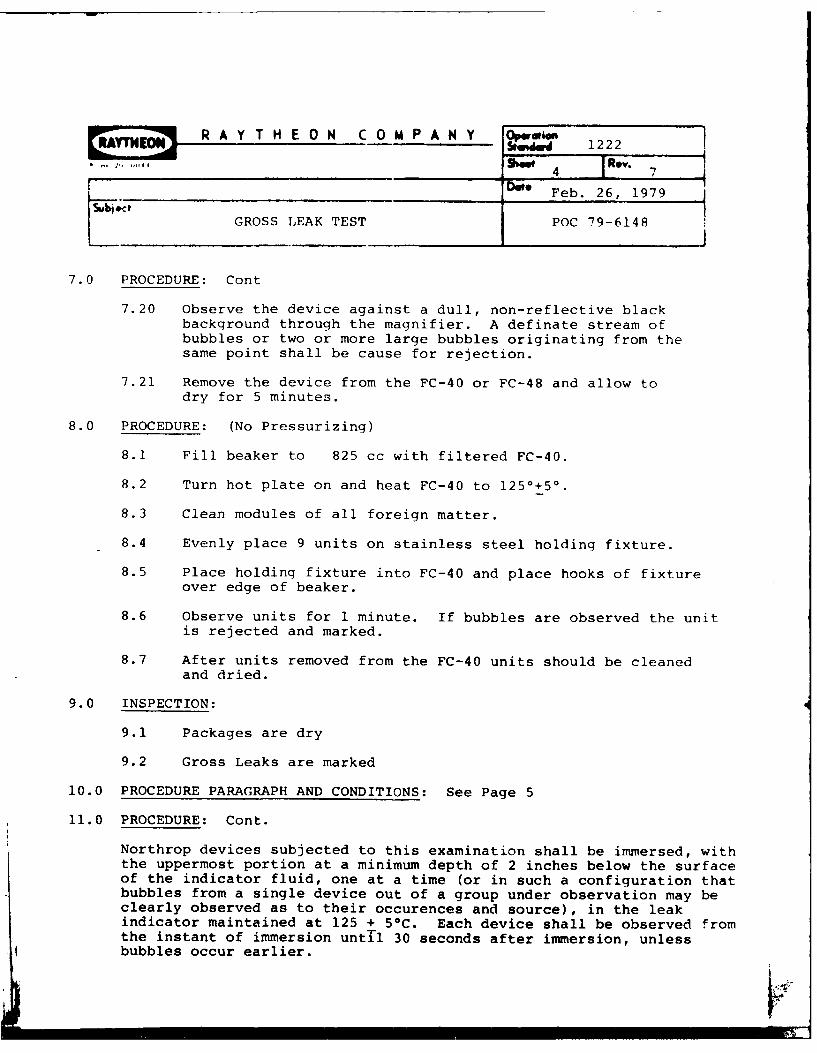
7.20 Observe the device against a dull, non-reflective blackbackground through the magnifier. A definate stream ofbubbles or two or more large bubbles originating from thesame point shall be cause for rejection.
7.21 Remove the device from the FC-40 or FC-48 and allow todry for 5 minutes.
8.0 PROCEDURE: (No Pressurizing)
8.1 Fill beaker to 825 cc with filtered FC-40.
8.2 Turn hot plate on and heat FC-40 to 1250+50.
8.3 Clean modules of all foreign matter.
8.4 Evenly place 9 units on stainless steel holding fixture.
8.5 Place holding fixture into FC-40 and place hooks of fixtureover edge of beaker.
8.6 Observe units for 1 minute. If bubbles are observed the unitis rejected and marked.
8.7 After units removed from the FC-40 units should be cleanedand dried.
9.0 INSPECTION:
9.1 Packages are dry
9.2 Gross Leaks are marked
10.0 PROCEDURE PARAGRAPH AND CONDITIONS: See Page 5
11.0 PROCEDURE: Cont.
Northrop devices subjected to this examination shall be immersed, withthe uppermost portion at a minimum depth of 2 inches below the surfaceof the indicator fluid, one at a time (or in such a configuration thatbubbles from a single device out of a group under observation may beclearly observed as to their occurences and source), in the leakindicator maintained at 125 + 50C. Each device shall be observed fromthe instant of immersion until 30 seconds after immersion, unlessbubbles occur earlier.
~~R AY T HE ON C OM¥P AN1Y Optio
Ndu - o~1222Fom 20-0044 Sw 5 1 Rev.
Dote Feb. 26, 1979subiect
GROSS LEAK TESTS POC 79-6148
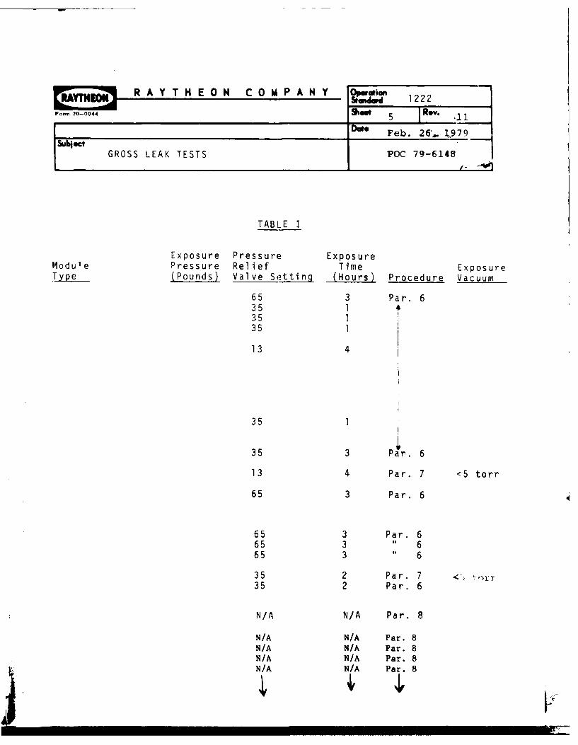
TABLE I
Exposure Pressure ExposureModule Pressure Relief Time ExposureType (Pounds) Valve Setting (Hours) Procedure Vacuum
65 3 Par. 635 135 135 1
13 4
35 1
35 3 Par. 6
13 4 Par. 7 <5 torr
65 3 Par. 6
65 3 Par. 665 3 665 3 6
35 2 Par. 7 ,35 2 Par. 6
N/A N/A Par. 8
N/A N/A Par. 8N/A N/A Par. 8N/A N/A Par. 8N/A N/A Par. 8!v
R A Y T H E 0 N C 0 M P A N Y 122R5AYTHEONC PAN Ydoawm 1222
F .-. -t ....... . w Shw 6 1 Ro,. 6
Daf May 1t 1979
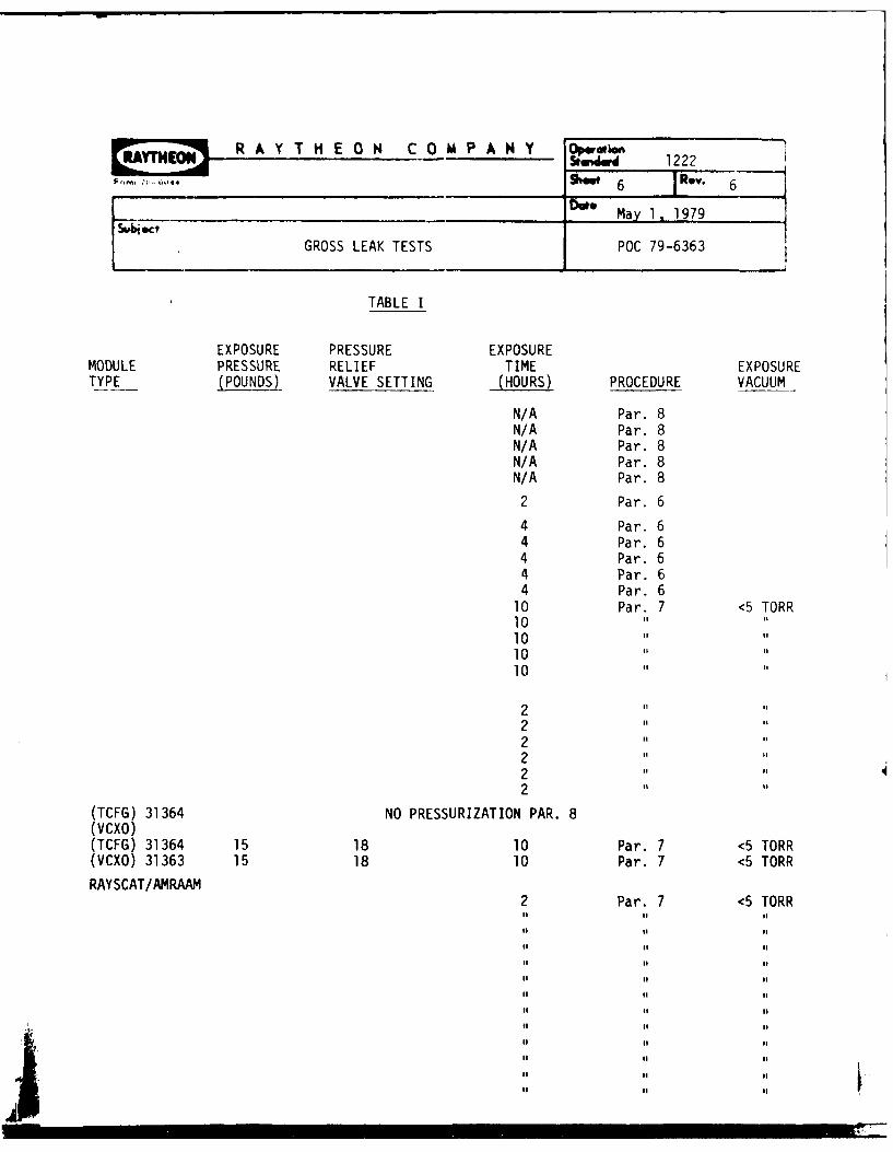
GROSS LEAK TESTS POC 79-6363
TABLE I
EXPOSURE PRESSURE EXPOSUREMODULE PRESSURE RELIEF TIME EXPOSURETYPE (POUNDS) VALVE SETTING (HOURS) PROCEDURE VACUUM
N/A Par. 8N/A Par. 8N/A Par. 8N/A Par. 8N/A Par. 8
2 Par. 6
4 Par. 64 Par. 64 Par. 64 Par. 64 Par. 6
10 Par. 7 <5 TORR10 ..1010II II
10II
2II Ii
2 i i
2222II
(TCFG) 31364 NO PRESSURIZATION PAR. 8(VCXO)(TCFG) 31364 15 18 10 Par. 7 <5 TORR(VCXO) 31363 15 18 10 Par. 7 <5 TORR
RAYSCAT/AMRAAM2 Par. 7 <5 TORR
|II, II
II II |
iI tI II
II II II
II l| II
II II II
II 6I II
. II II II
II II II
II II IIiiII II II' I IIII II II III •111
R A Y T H E 0 N C 0 M P A N Y 1222
Form 20-0044 So _ Rv
_ _ __ _ __ April 5, 1980
GROSS LEAK TESTS POC 80-4300
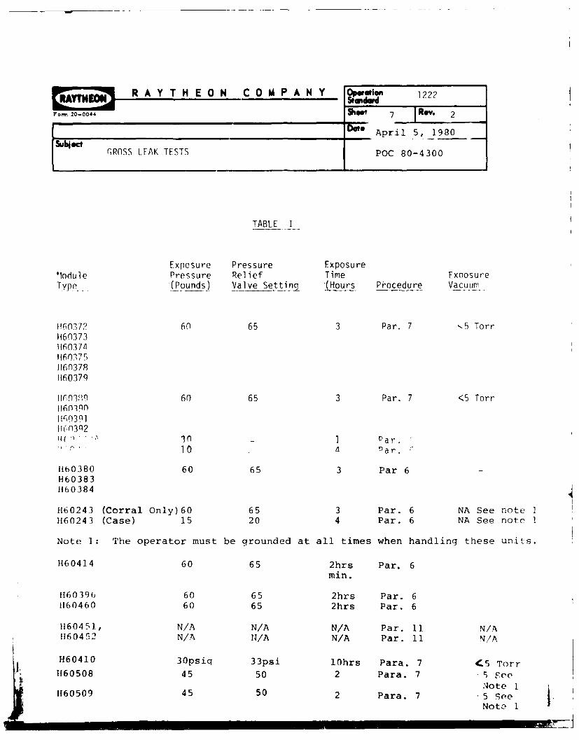
TABLE I
Exposure Pressure Exposure!1odule Pressure Relief Time ExDosureType (Pounds) Valve Setting (Hours Procedure Vacuum
1160372 60 65 3 Par. 7 -5 TorrH603731160374
1160378H60379
11r03" 60 65 3 Par. 7 <5 Torr116n3n11r0391llt o30]
i _. 1. Par. ,10 Par.
1160380 60 65 3 Par 6H60383H60384
1160243 (Corral Only)60 65 3 Par. 6 NA See note I
1160243 (Case) 15 20 4 Par. 6 NA See note 1
Note 1: The operator must be grounded at all times when handling these units.
H60414 60 65 2hrs Par. 6
min.
1160390 60 65 2hrs Par. 61160460 60 65 2hrs Par. 6
1160451, N/A N/A N/A Par. 11 N/A1160452 N/A N/A N/A Par. 11 N/A
H60410 30psiq 33psi 10hrs Para. 7 45 Torr
U60508 45 50 2 Para. 7 5 Fee1 Note 1
1160509 45 50 2 Para. 7 5 SeeNoto 1
- t
R AY TH EO0N COM P A NY 0p~w 122
Fon,, 20-0044ShwRv 0
suj GROSS LEAK TESTS POC 79.-6148
Vacumlvev
ViAve alv
1//8 I.D.
Copper Tubing
250 ml600 MILBea ker Bea ker
Fig. II
M 20-804410 31
'___ August 10, 1979
HELIUM LEAK TEST POC 79-6576
1.0 PURPOSE:To specify a method of testing the leak rate of hermetically sealed
hybrid circuits using a Helium Leak Detector.
2.0 SAFETY:
2.1 Normal precautions; no unusual hazards exist.
3.0 APPLICABLE DOCUMENTS:
3.1 Test methods and procedures for Microelectronics - MIL-STD-883,Method 1014.
3.2 Veeco Instruments Inc. Operation and Maintenance Manual for appropriatemodel.
4.0 EQUIPMENT AND TOOLS:
4.1 Veeco Mass Spectrometer Leak Test Station, MS-12, MS 17AB orequivalent.
4.2 Sensitivity Calibrator Type SC-4 or equivalent.
4.3 Pressure Tank, fitted with a helium inlet port and release valve;tank to withstand 100 p.s.i.g. pressure.
5.0 MATERIALS'AND'SUPPLIES:
5.1 Helium tank
5.2 Circuits to be tested
6.0 REQUIREMENT:
6.1 No helium leaks beyond limits as listed in Table I.
7.0 PROCESS PROCEDURE:
7.1 Pre-Operation Procedure:
7.1.1 Sensitivity Check: The sensitivity check must be made usingthe air equivalent leak rate figure printed on the SC-4 typeSensitivity Clibrator.
31 3 5 0 15 7 5_ _ _ __i _
0RAYTHE N COMPANY _Cort.
F- 20--0044 Set 2 1Rv
:Date April1 23, 1975
Sbjet POC 75-609 5HELIUM LEAK TEST
7.0 Co nt .
7.1.1 Cont.
The procedure for this check should be in accordance withthe pertinent manual. This check must be performedbefore using the equipment for leak testing, and re-peated at reasonable intervals (at least every 4 hours)during the day and at the end of the day. If sensitivityis incorrect, refer to Manual for correciton/calibrationprocedure,
(Note: Usually addition of liquid nitrogen to cold trap returnssensitivity to desired level)
7.1.2 Pressurization of Circuits with Helium:
7.1.2.1 The units to be tested shall be placed in asuitable container inside the pressure tanksand the tank capped ti'ght.
7.1.2.1.1 For units requiring 60 p.s.i.g. pressurization(Table I), check to see that the helium tankpressure is at 60 p.s.i.g.
7.1.2.1.2 Open the valve to the pressure tank. Thenslowly open the release valve until escapinqgas is heard (not a rapid ventiqg), vent for4-5 seconds and close the release valve; thenrepeat. The pressurization shall then bemaintained for the required exposure time.
7.1.2.1.3 For units requiring other pressures, adjustpressure regulator to desired level, (Table I);then follow procedure of 7.1.2.1.2 above,
7.1.2.2 At the end of the exposure time, the helium pres-sure port shall be closed, the release valveopened and the units removed.
7.1,2.3 The units are now to be leak tested within the
time limit specified in Table I.
7.2 Testing Procedure:
7.2.1 The helium leak detector must have been checked andoperating in AUTOMATIC mode for at least 1/2 hour priorto testing. PushFthepump switch to VENT, remove themanifold plug and insert the appropriate test plug intothe manifold chamber.
J ,'' ' , II l I
R A Y T H E O N C O M P A N Y aiLStdord 1229
F.- 20-0044 Shew 3 Rev. 5
Date April 23, 1975
,biectHELIUM LEAK TEST POC 75-6095
7.0 Cont.
7.. unitsJ tu be tested in the gasketed tube andinsert into test plug.
7.2.3 Press tha FILAMENT EMISSION "ON" switch, if it is notalready ON.
7.2.4 Switch the LEAK INDICATOR knob to the required SCALEfor the particular device(s) being tested.
7.2.5 Push the pump switch to START and wait until the TESTlight on the LEAK INDICATOR comes on (usually 15-?_5_--sec.';then read the LEAK RAT-E
7.2.6 Units that read greater than the test limits in TABLE Ishall be classified as leakers.
7.2.7 Push the switch to VENT and remove the unit(s),
7.2.8 Repeat for additional circuits.
7.2.9 Special Cases:
7.2.9.1 If the TEST light does not come on in a reason-able time, i.e., within 30 seconds of pushingSTART switch, there is either a large leaker ora Teak in the system.If the FILAMENT EMISSIONlight flips off, the same conditions could exist.If either of these conditions occur, immediatelypush/to VENT; then check for leaks in the systemand repeat the test on the unit(s); if the sameconditions happen again, VENT and remove theunit(s) under test which shal then be classifiedas leaker(s).
7.2.9.2 If, when the TFST light comes on, the indicatorneedle slams oT-f--scale, immediately push switchto VENT and remove the unit. The unit undertest Wall be classified as a leaker.
7.2.9.3 When testing more than one unit at a time, ifthere is an indication of a leaker or the con-ditions described in 7.2.9.1 and 7.2.9.2 thenthe batch shall be Immediately retested one unitat a time to find the leaker(s).
Note: When finished testing the lot(s), replace themanifold plug and push switch to start.
I In inllI nl ninF
R A Y T H E O N C O M P A N I .w, 1229
Fom 20-0044 Ueet 4 Rev, 0
Dee April 23, 1975Subject POC 75-6O9-1HELIUM LEAK TEST
8.0 MAINTENANCE:
8.1 Refer to Leak Detector Manual for General Maintenance
8.2 Start-Up:
3.2.1 Turn on ELECTRONICS switch.
8.2.2 Fill the cold trap with liquid nitrogen.
8.2.3 Turn the FILAMENT EMISSION switch ON.
8.2.4 Allow the leak detector to operate for 1/2 hour beforestarting to check sensitivity.
8.3 Run sensitivity check at start of each day, and at intervals nogreater than 4 hrs., plus at the end of the day.
8.3,1 Push switch to VENT, remove manifold plug and insertSensitivity Cal--rator TYPE SC-4 into manifold.
8.3.2 Turn leak indicator knob to the scale corresponding tothe Air Equivalent Leak Rate, tn STD. cc/sec. as printedon the SC-4 calibrator
8.3.3 The calibrator valve, even when not being used forsensitivity check, should be fully opened; check to becertain this is the case.
8.3.4 Push switch to START and follow SENSITIVITY CHECK pro-cedure of Manual,
8.4 Check helium pressure tank supply; also, weekly or as indicated,check for leaks in vacuum-pressure tanks.
8.5 Shut-Down:
8.5.1 Place metal plug into manifold.
8.5.2 Have switch tn S7ART posttion, with vacuum indicatorneedle below the red indication area.
8.5.3 Turn off the FILAMENT EMISSION switch.
8.5.4 Turn off the ELECTRONICS switch.
niim
R A Y T H E O N COMPANY OW2kutda i?20
Form 20-0044 5_e 5 154
J b D . A il 9, 1979
HELIIIM LEAK TEST POC 79-6269
TABLE I
HERMETICITY TEST CONDITIONS & LIMITS
Exnosure to Helium
Dwell Tcst Limit, Max.Time Mdasured Leak nate
Pronram Module Type No. Pressurc lime Max. cc/sec. He
60 70-40 Min. 90 Min 5 x I0-
60 1F Hrs. + 90 Mmin 3 X 10⁻⁶
60 16 firs + 90 Min. 3 x 10⁻⁶
60 2 Hrs. 30 Mn. 5 x ln- 7
60 -0-40 Min. 90 Mn. 5 x 10⁻⁷
60 16 Hrs. + 90 Mn. 3 X 10⁻⁶
60 20-4n Min. 90 Mn. 4 x In-7
60 16 Hrs. + 90 Min. 3 x In-6
60 3-4 Hrs. 35 Mn. 1 X 10⁻⁸
30 30-40 Min. 90 Mn. 1 x 10⁻⁶
30 16 Hrs. + 90 Min. 2 x 10⁻⁶
10 16 Hrs. + 90 Min. 3 x 1n-6
in
10 4 Hr. 60 Min. 5 x In-7
10 A Hrs. 60 Min. 5 x 10⁻⁷
60 2 Hrs. 90 Min. 5 x 10⁻⁷
60 12 Hrs. 90 Min. 3 x 10-F
60 60 Min. 30 Min. 5 x 10⁻⁷
Max. Max.
60 2 Hrs 1 Hr. 5 x 10- 7
R A Y T H E ON C M PAN Y 1229,, 20 0044 6 •f~w 7
Deft August 10, 1979
HELIUM LEAK TEST FPOC 79-6576
DWELL Test Limit, -Max.TIME Measured Leak Rate
PROGRAM MODULE TYPE NO. PRESSURE TIME MAX. cc/sec. He
60 2 Hrs. 30 Min. 5 x 10 7
60 2 Hrs. 30 Min. 5 x 10 7
60 1 Hr. 60 Min. 4 x 10 7
30 4 60 Min. 5 x 10"710 4 60 Min. x 10 7
30 1 Hr. 60 Min. 1 x 10 830 3 Hrs. 60 Min. 1 x 10:830 1 Hr. 60 Min. 1 x 10-830 1 Hr. 60 Min. 1 x 10"830 1 Hr. 60 Min. 1 x 10"830 l Hr. 60 Min. I x 10"830 1 Hr. 60 Min. 1 x iO-830 3 Hrs. 60 Min. I x 10-830 1 Hr. 60 Min. 1 x 10-830 l Hr. 60 Min. 1 x 10"830 1 Hr. 60 Min. l x 10:830 1 Hr. 60 Min. 1 x 10"830 1 Hr. 60 Min. 1 x 10"8
This is the max. time within which all units in the lot exposed tohelium must be testedin the leak detector after removal from pressurization cycle.**For Q.C. Final Test Only.*Alternate Fine Leak Test for all Santa Barbara.After removing from pressurizing bomb and before Leak Test, flush parts with dry nitrogenfor 30 seconds minimum.
30 2 Hrs. 90 Min. 5 x 10:760 2 Hr. 90 Min. 5 x 10"7, 2 Is. 60 In. ljlO'8
60 2 Hrs. 90 Min. 5 x 10"7OR
60 12 Hrs. 90 Min. 3 x 10"6
60 2 Hrs. 60 Min. 5 x 10"7 See Note 1
15 4 Hrs. 60Min. 5 x10⁻⁷ See Note 1NOTE: Operator must be grounded and a deloniztng blower must be used. It shall be
aimed at the test plug and be not more than 2 ft. away.
~R A Y T N E 0 N C 0 M P A N Y O0aqRM PSiandwd 1229
______ June 5, 1979
HELIUM LEAK TESTS POC 79-6442
DWELL TEST LIMIT, MAX.TIME MEASURED LEAK RATE
PROGRAM MODULE TYPE NO. PRESSURE TIME MAX. cc/Sec. He60 lbs. 16 Hrs. 90 Min. X
15 Psig 16 Hrs. I Hr. 5 X 10⁻⁷
30 Psig 5 Hrs. 60 Min. 1 X lO-7
3 Hrs.3 Hrs.3 Hrs.3 Hrs.
60 Psig 5 Hrs. 30 Min. 2 X 10⁻⁸
'0 Psig 2 Hrs. 3 Min. 2.4 X 10⁻⁷
ECOM H60388 IFp IFlI(32157-3) TCFG 30 Psig 2.5 Hrs. 30 Min. 2.2 X 10⁻⁷
(32157-1) VCXO 30 Psig 4 Hrs. 30 Min. 2 X 1O-7
30 Psig 2 Hrs. 30 Min. 2.4 X 10⁻⁷
30psi 4hr. lhr. 5 x 10⁻⁷ cc/sec
.1-
R A Y T H E 0 N C 0 M P A N Y Ow rS:INDUSTRIAL COMPONENTS DIVISION k.dw I
Form 20-0044 i 1 I Rev.Date Aug. 13, 1)-4
MiedPOC 7- 191'-PROCESS INSPECTION RESISTOR TRIMMING
1 .0 sCOP :
Ihis instruction details the inspection procedure to be foll),edin performing resistor trimming In-Process Inspections. Alluperating machines producing regular production substrates artcovered by this procedure.
_.0 APPL ICABLE IOCUMENTS:
2.1 O.S. 1018 - Resistor Trimming Procedure
2.2 Applicable screened sub.-trate drawing.
3.0 IFQU 1PMENT:
3.1 Microscope 1OX to 30X stereozoom or equivalent.
3.2' Six (6) place digital multifunction meter or equivalent.
j.I yREjUE~tlY OF INSPYCTION:
4.1 "Set-Up-Check" - Start cf shift and change overs.
4.2 "In-Process" - Every half hour of operation.
5.0 SAMPI.L SIZE:
Five (5) substrates to be dran from most recent production.
0.0 AREAS TO BE INSPECTED:
6.1 Electrical:
Resistor being trimmed and all other previously trimmed resistorswhich have a tolerance band of ± 1% or less and are within l'4inch of the resistor being trimmed.
6.2 Visual:
6.2.1 Resistor being trimmed and adjacent areas.
6.2.2 Probe point areas (Use backlighting)
6.2.3 Entire substrate area for overview
2 3T. T .... W......llll | IIII 4nun______ H___m
IM R A Y T H E 0 N C 0 M P A N Y OlPWaiINUSTRIAL COMPONENTS DIVIION
Form 20-0044 2 Rv.Dote Aug. 13, 19-4
IN-I1ROCESS INSPEiCTION RESISTOR rlRIMMING O
0 DISPOSITION:
If a defect is found in the sample the process shall be shut d01,wnand corrective action taken. The process may not continue until isubsequent sample is approved. The inspector shall report an\"incidence of non-compliance with this provision to the inspectionforeman.
8.0 RECORDING OF DATA:
Electrical and Visual Inspection data shall be recorded on the da,:Asheet of Appendix A.
9.0 CRITERIA:
9.1 Electrical:
Resistance values shall be within the specified "post trim"limits guard banded to 80% of the total range.
9.2 Visual:
9.2.1 Check to 200, 300 and 400 series criteria of (.S. 12o3and also items 501 and 504 (Glaze overcoat) of ().S. 120>-.
IUCI
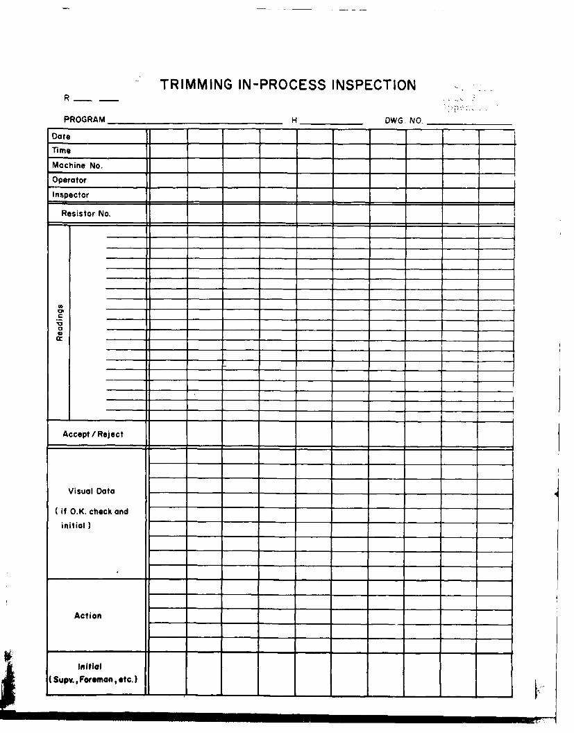
- TRIMMING IN-PROCESS INSPECTION
PROGRAM H DWG.NO.
Dote
Time
Machine No.
Operator
Inspector
Resistor No.
Accept /Reject
Visual Data
if O.K. check and
initial]
Action
Initial( Supv., Foreman, etc. )
RAYTH £0N COMPANY OpIeiRAYA YEO ! m 1253
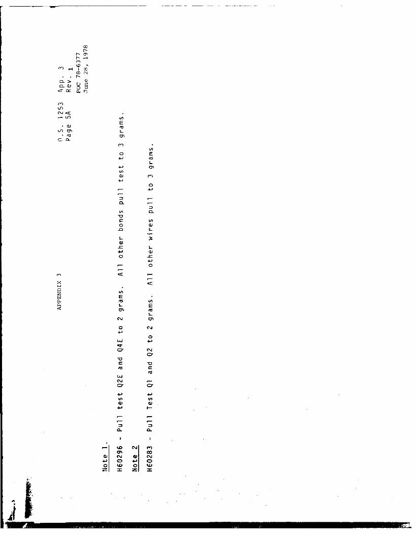
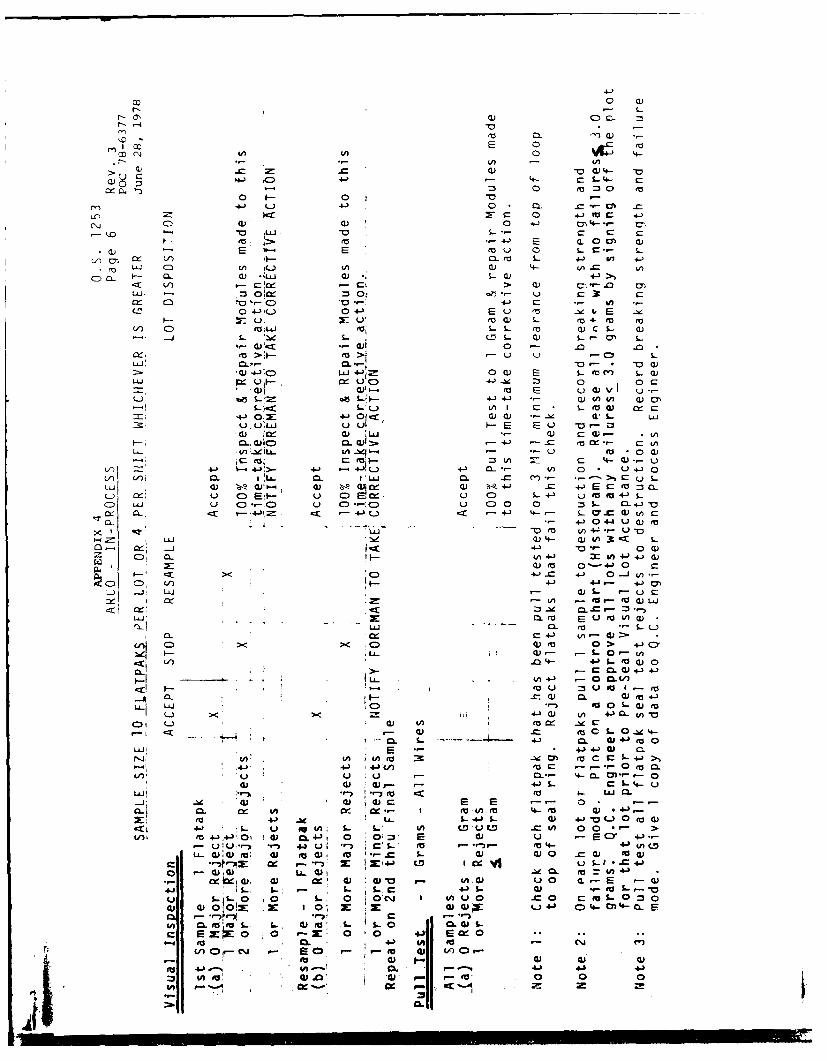
_-_ 1 Shoo I 23Dot* Nov. 27, 1979
PULL TEST INSPECTION POC 79-6907
1.0 SCOPE:
This instruction details inspection procedures to be followed in performanceof Wire Bond In-Process Inspection.
2.0 APPLICABLE DOCUMENTS:
2.1 100% visual per MIL-STD-883, Method 2010.2, Condition A for I.C.'sand MIL-STD-750B, Method 2072 for transistors and diodes.
3.0 EOUIPMENT:
3.1 Microscope B L 31-26-94 or equivalent.
3.2 Microscope, Metallurgical B L DMET-31-20-37 ro equivalent.
3.3 Non-destructive wire bond pull tester, Mech-El or equivalent.
4.0 GENERAL PROCEDURE:
4.1 The Q.C. Inspector will obtain the required sample for visual inspectionand pull test as specified for each program in the attached appendices.The sampling must be spaced evenly throughout the lot run and mustinclude a piece at the start of each shift; a piece after a stopcondition. Before performing the wire bond pull test, visually inspectall bonds at 30 to 50X magnification in accordance with the criteriain O.S. 1265. Major defects as those defined in Paragraphs 3.1, 3.4,3.5, 3.6, and 3.7. All other defects are considered minor, for In-Process Wire Bond Inspection. Disposition of the sample is in accordancewith the applicable appendix. Unless specified otherwise, pull testall wires on all modules even if they are visual rejects. Identifyvisually rejected bonds on the pull test data sheets.
4.2 Machine Shutdown - When a stop condition is reached the Q.C. Inspectorwill notify the production foreman to stop the operation and takecorrective action. The process engineer must approve machine operationbefore wire bonding is resumed. The Process Engineer will recordthe action taken and initial approval on the pull test data sheet.The Q.C. Inspector will then resume sampling with the first pieceoff the machine.
23 9~ 1 2 2 1 J002F _._.. --- , 0 ..
12 3
-DeJune 28,1978
PULL TEST INSPECTION OF POC 78-6377
WIRE BOND OPERATION
4.0 GENERAL PROCEDURE: Cont.
4.2 Cont.
The Process Engineer will record the action taken and initial approval
on the pull test data sheet. The O.C. Inspector will then resumesampling with the first piece off the machine.
If all failures are ball bond lifts on a particular chip type and the
Q.C. Engineer and Process Engineer approve by recording on the pulltest data sheet, continue processing ard sampling but mark the lot for
100% pull test of that chip type. If the same chip type fails on sub-sequent samples of that lot it is not necessary to use re-sample procedure.
4.3 100% Pull Test - If all wire bond failures are ball lifts on one chiptype, 100% pull all chips of that type, If the wire bond failuresoccur on different chip types, 100% pull test all chips.
All module failures from 100% pull test will be reviewed by the Q.C.Engineer and Process Engineer to determine repair action and disposition.
4.4 Sample pull test after 100% pull test and repair.
Resample all modules subjected to repair to the sample size specified
in the individual appendices.
,,41i I iII q-=
-cm Z3 0 czCID4- ' ) r4- I2K 2
0:0
IJ > I I-H CC)
LC) a).. a)
--- -- -0 - 1F
a)+' O 04) 4LV) 00W 00W I -16.
cc imQ) a cli4JI
V) CDC +4-) Q) 4- - z
LYu U 1L 0 L 1I i cu :.
X Oz~ S.- C. - )(
LuJu LuI
Z (E
CL IC r LuJ I~ LU C -2
C- - Lu
LiLu
<-JLLu C
Lu))CNJ >< 0)> > L
N.D 0L 0 A -
(A -L
4- ) 4.) 4Je (a . U)) 4
~(J 5U4. - . ~ ~ ~ ~ 4) 0
(1) yL )UJ0 + O E CO. cl .) co F, 414CL- 0J0 00 4.4 Q
V ~) 4J 0 (U (U 4- 0- 0 aL-v(u C l
-~ c0u cu IV (D' :3 (U0 (aE L*t-(Um MenQ0 =. 0Y m, Ln .u L
o~o 0 )0 00 -) 0) 0< -r w ( 0) ME I= 1.. X:na
S- C" S- 0. . 4J +J L~O - S.. (a.. 4C .CC-
(U I- r- , "U- L-*4- to to S-' S-4 )( ( -()
4- CA' 4J,
Xy (A w w
(A. n- -LJ -.=3 00 E00 EL
00 4-0)o a0m0
(VJ CDI Li c V
CD 0- We Li ra
a) ) 4-) 0)' a C): L 0)c
(U ,-- IV L
S-fl So n EL; LL oL-L 4- o4-) 0 aC, (AO Of a) (Vl
U u L )
4-) WU 4 C
0 ~ O.0 U-~ ii :4-) 4-) -) 4-3 O-' OW' 4- < a CL OWCL IE Lj)-i
2- L a) a)u ~ CDL EE4-u'Z4--- u C) 4. ur CD- i - D-
L C)-x D- x(ADro uC (v I l :r U inc)rL:r 4-0X 4-O Ei Win ) <C E
V) W) L&C L)~ L
Lii in --
L-) LX CL Ij CLC O i
Of oCL W-<)~ WW W 2 L m
C) L
)~CD
ci
CD
Li V)
F-
Li
Li Li
LC : -(D)
(A V) oS-I
a)) Li OL Ui (A v
L1F-- ex Ix VJ.-- S- 0) r V .. t
41 0 (V - 0- V) G) r ( aX- a)O I Um . -0 I Lv
L/)(U 0. -uCr o rAi w( v a r v a 0 A L n( n V Aa
c c!0 01 0 c
Cl) C -
N .- > ->>
CD- Q). C> C0. 0 l uG L--u.) S-
al 3 J 0 C- ). ) .- 0 CUC41 -c L.t .M6
ul_0M L4 -0 4) 0 0 a 00)j *LU 04 to U cxu uu
0 L .) ~ 4 -' c - 4 -
CD a.0 Cf :3 c
wU - 04-') 0 4-) -E E E2 2E E EF- (A M: uU ZEu a. ( e4: C m eLUJt aLUJ S-4-' )- =~M LU Q- 1.. : 5= CD C DCLLU V) IA (D-0 -C 4A(AA
- to -(> (0> I. %J* ~ C'j .-
V) (A G4- C 04 '0 C 04' 0 4 04J 0 4-!L- I- FU - CICU - 4-) 4-) 4-J 4-'LUi C 0 000
cn LU :c S-. (A () LnL lA2-4)0 0)0 X:0
LU i LU U LLU ULUJ I--0 I-0 a-* I-0 -(A 4 ) ) Ofw wio (a ro r fIC- a)~ C.) 0.4)0 C) E E -El
-(A -11 (A LL- (A..e - --.
Uj n4 4J. -. >-. ~ 4-) -3>- 4) 0-) 4-) 0.0 ) 4)00 Q- ) CU -ja! <m. I C0. LL C. -0 CL 0. - 0.L -
(v I- 0) (0) , 04 e 0) 0)sk0 :3 0) ~C7, LL U CD E- uC>E F- U00C 0-0 Ut U> 0-0 u Du U : 0- UCD UOO 0 uC D0 u CO U ) : 0 :
Cd) V)
LO
-j-
LU 0.04 -cc 0._
;- . -jL- - --
w- CZ2>
IX (n (A e
VA In) (.3 0
0) to)4
j P .
C'~C LU UU
0) ".. 4 ) (U 0) wU. -
to C r, (S (A (A (AV) OJ ) 0) QJ3 -c r66 E E =E E E CE 6
'U LL. S.. S-)-' (A L CD c OCD CD CD CDOD C0D LD tou CD (D+A (A UU C WU +j -.- (0*~C* IA) -- ;, c-E
OU (A -) -_ - 5= 1- r-' E( ---
c.. )0 0 CD 000: ..a Ci w 1 0) w WE IA WA C(A CA 4) "
i-. L- o= m- 4-J 4-) 41 4- . 4- 4-) 4-' S-CD L. 5== 0 o UU U U U -U U 0
(A 0C c 2 0 M: I-4J I 0304) 0) 0) 0) 4) 0) 0) aa) -) 0 . 1 wU 4p -r ) .1 r ) f. - r-) .1.1.. (A.
=-W, > to J-S- 5= 'S- L ) 4J ..*.0I0V dl 0) 0D 4)) 4) dia,4aX0 0. 0 a 0Z CL 4A 0L-C -Z.- r4 c:c6 ~ r= 03 E - Stu C) CJ CL CD0 to CD EU Cj V 0.0 -(V) cn 2 -
4.( A -4--0 ra (Atn' tv. W U)U0.0 r_
cc Ix4t4
IrND>
C'-G)
U-))
E
V) U) S
0 E.4-)t
4-)
(U
4-'
0 a
4-'
0.
CZ
W E)
S.- E
.0 c..4-) 3
o 0L 4-)
- 0
1-4j
eazL
oo
4J Co-j C
0 w 0
OD 0 a)
-
L
01000E 0
ase Va)-
4- ~4-) - 4- S%-4-
0 11-- 0 V-4- *~)4-) 0 * a- *.CM
Lnc 0 4-)EU vu : -)C C (L) 0) 0 +' o'-e -
-~"0 U -o 0CF-( ' --:I- u4-' (L c~0 a)-E -'E ea 0 s-r- S.
LI ) CL ro 4-) l 4 )
LUj C) 4 OL.) ul(3) 4- V).E U
c a Cl - CL a) !LUj a . Q.) 4->-C - C'Ox C > a) ~ *-.0 o
LU. -3 O ~ : ,. L) U -C3 ccc m' 0v I- C 4-) a In V *
C)! 4+-);(04- E U m .. 4 Er- ~ U. e%3 rW S- ro + ru ra
V) L. to ;W. M CU)S Q) C0 L-4.S3 - (D1 S- ) S - 0 S
IX, m:-' >1 'U U - C)LU. CL- l 0- Va
L.U4j!= 0OW E S-VC LWmS-QLU =U- ~ u I C)---. : 0 cC
-) I) mJs- E-= Uw v' U--4- -a4-) 4J Winy cn Q.U, <I I C - m wU Of~
4j Wa 1oirG) II -. c CL I- LUU.Ul&J U U. v
DL. a) LU ) CL > r V
.4n- U-i ILL in-4 g 0 a)
V)4-) +-4-i> 4- -4lL - .~ -- 0 ) 41 oL/ 0iC. ILL. CL IL& 0. C 'h. - ,
LU~~Z a) to) =) m 3 ) 0 +E EL. ;u C 0EA- u C) w! U CD L 4-' U (0 #04-'L
CD wU U C) .- ,-0 u On*C) U C)0 0 ~L0-4-0Ql CL. c - 4-. CC - L- CC 4- 4-- w o 0 a c
0- w Q) -- a O ) : c S
7- V) 4-) M+ 4 L
Q) r 0-4J 0 C:0<C 4-)..= 4-) 0 -Juf).-
C) C). (-) 4- 4-i-)J LU S) U
LU- 0. EU fu "A
c C 4-) U. "-
Ln C) X () ea 0 > 4J C)I:ILLU Q) a)- 0 'uA
V) .04- 4J 6- M ) 0a. - CL 0.) 4-) 4-)
LL 4 4- 00 CL V)vU-
CL'0 42) 4-'0
t 1
-< 4J ' C 0- -0
-. 0. L- 4--3- D. G4
) 4J O
4-) . 4 4-) 4))/ r_ -" ( 0
U- Uj j -A m. r_-- 0 ea -Ou) u Qa) CM, -4-i oL
- 4e Cu a) 4)C c 0 -0. ii I=. IA E w 0 (a 4-E a)0 D
X'U 4-1 . LA-S -,S (U) 41-1 -)0 - 0 ea(-C1 4-) S- Q fgu 4 .- L LA I DuL EDf 0 0 *1-
eO) '4..),4-'01 @3 CL4-3, 0 o. E IS U - E C ..---
- u I u -- , r) 4.a u~ *-r) r-' EU .- ) II- ea 4- 4-' (A C-L- 4): ) M d On o).3 EU '*- = ~ S- 0V0 to EU
W , . Z XE4 CM IcV USIV; = 4-)O )03 LL. ) 1 'O C. Ma 4.3
Ix. kx 43 w 4) @0 "a 1- tLfCUP U 0 (L E -0C3.4J)I S. $- . - S- r- 4-iS- to S --u L%-0 0 L. 0 OC 11.J inU cC CEL 0=0) (L 0 00
1z Z I 0; : - 4) (v ;E3 L
4- C) 4- cm4- Q-E
'VCA
V) EUr ON1 3 C) 0- ou 4) 0
to 4J ~ U 06 41 4.1 41)tA M!EU 4).0: W3 e -E 0 0 0
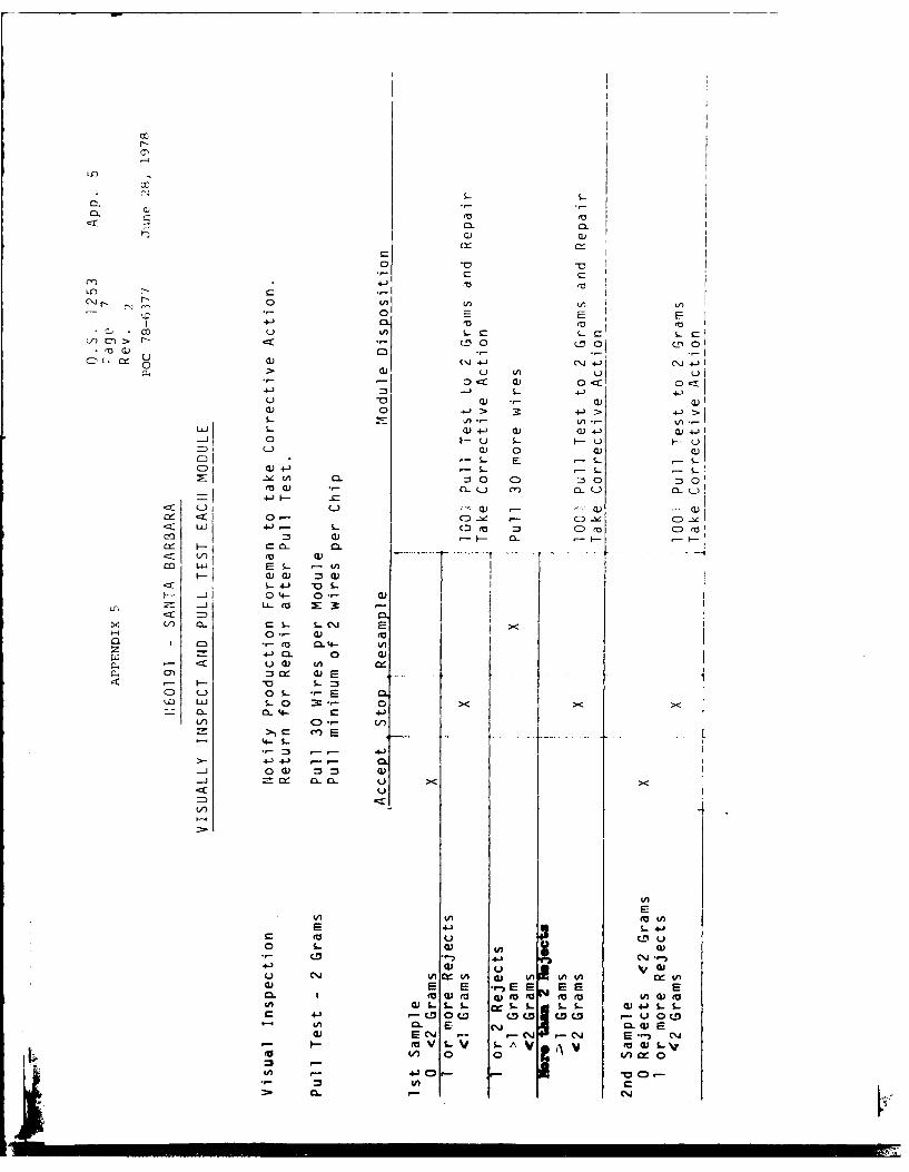
C) )
CC
E El4ca.
u LnSCCIO (L) z
U 0 (i 4.J C'.0 0
4- 4J (AU> 4-) > ~ 4)o o
4) 4) QL4) -
a) 0 0C:) - E
W4-).- S_CL=3o CD 0o 0
.::I: *' 4 CX) CC a :n I) - - F
C).: c0-.__ V) ca.- a)~ ~
cow ELS -(A
L-.4-) -0 SI- j 0O4- 0* 0D
(.1 27 _j . Ca XC\ E
x 0- Qc S_ S- )0~~C I n .4- ()
4- CL 0 0)u u0) (A
I-0) b.J LO 0 0 >
4-)O 4- 4-)
- ~ C 0V )
(A .41
(AE
C Ln (1u
4.J ) u 'VGu (NI CAA 0) (A vi I^0) E E *-E E E E E
L . S_)t 0) SU(A c
C. C)~ - c CD c c Dm .- UoCDCA 0. E C* 0L0) E
0) C14 - .- C14 ,CIJ E.-j (NIto- s- mVV AVr U
*0 (.) o 0-A V)~ 0
IA 4J 4. C)*1~* CA
>. o -e.
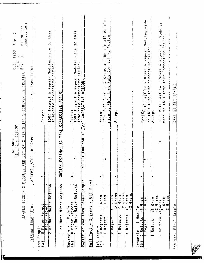
I '
z 0
CL ii(L0)eu C>4
*~ Q) Q,) C)a
4-) 0 .61UEoE
CU -QLO )C
LU C. ~>.. \.J 4J (\j ~ cj .Of L/ C-) CL -) IWO ~ O
n u u -1.41F cl1
WL) (,- (D. i Y
S- - S- 1,i 1 L4-) 4-0 I- 4 OLUJ a)'W a)
L CL) CL CU 4C ,z0 ( .c LL LU U-LU-rea c e C' LL :30 0 A
- 4) -4 4- 4 -) , JQ - 4-) o-+-CL 0. 1 I- n ~ Q.C. -
C -) C. ) C) W (L) CL a) Q)W ) WUU) CE LU UC)EL) 0 C) U 0 UI 0 X
F- u C) O C . L) UCD ea U u C ' u C 0 <
(V) I ,
i LU LU
C)
I LA-
-.1 C:
CD CU 4< U <>
C C U-
ci i- aJ
L-) >- 0<>
-J LU C
CD < ) tA
LA ~ ~~ ~ C). 0 S - .
4'J +- 4) E
C) a) ) V)t
rr)- - V) 4A 4ALUj a) rz C-- E E E EEE E
to to ea( a u( E E E E E ES.. L.L L. L. L- LL L.L.4t . mLc
4-' 4 0 4- 0 UL- tv( C5 CUCD~.' U)LUJ C UU' C ) U "-, 0 - CJ ..- ('J -e C1 ) a)
- Q)' r to3' a)t E V 1. A VA 'A V e-J c)(j 0.
cc LUJ (D C) ow W 41~ CD InI n 0 CLnV) 0.. L. S Z s- 4J 4- 4. 4-A + 4-3 Em)C
It) 5- S-o 0 S- 0 u~ U U u U 4-) 4-) 4.) ).o 00 : 07 W) 4)) (D 4) -UU U 0 mV
Wto' S- - I'V to - WW Wi W3 (D . .-" .1.- :. o 0 0 CO 4.) -W Wa 0 j4 ) 1- .L
C 0 a 0 $A . (Uw 0
Cl, Ma 0. 4 I- to (NJ- - "
'a M, - ,
4A to) I
C4 M
0 C)
r-'l 4-) C) 4 CX-> x U oU-
a)F U%0 -
-r->
- 4) (a -4a -
-' 0 LJC o. 0 -
CD a) woSaj -,. -o L -0 0-0.e
(30 O= I0~ .WF-2 CD" - CE' .- 4 0- cn.a
r~j of -o .- C0 to0 W4-) (4-1,Ne S- le C.D 0 .
C) a-) zc.- 0 L
0-~~~~- 4-') 0-L 2~~~~~ 0UL) ~ 0--
oZJ 0- 4- OL.FOi).4-) 4-'4
4- : -) M a) a) ) aU L L/) I- 10 41 (J- --a)r = a) =-- ea*. -
4 0 0- C CL* 0 D C. E-4'LU :3 -4 L)* 01 L
0 -4- -)4 - 0- a)4- 41 LU LL " LL- C l) CL
F. - -0 a) LJ I--v-(I vZ ,:
-) C) . C ) 0 -- . u (0 u )
CCD CE fU
C) CD V)- 0 2 -F. ' Ct
(I ) C) 0>-C oo - U 0 u
C) w-
Lm >< :KV A <>
(A V) ul V)to40 4J LU4; -
u 0.
F..- 0)
:3. cc/ 0 A nC
C) LU) 4J.1 0 0 1- m L3C
V) 2,0 oM C o - ~ I l
Z'-. LUi &-
I4 (. a
F-' 4-. 4- 0-1 4J 4J 4)4- -
< I-S U U u C~ uo, ON: 4-) a, (VLL 0) 4)0
LU o 0a , a. UU ) )U-1--4 s-. to 0. 4J 0.5 W2 W
cxx xi. o-4- 0 a4.7:0 0 CL CDC mm cca, Vci Ix
C1. toa Ca, CD 0~ a z~, a~ U U EU )
2. 5 . 50 (4c ~ 4'-5-1 - 4A -50 4 4A0e.
CA to 2 2: 0 : :-' u @3, aaa
IL,.,-,e*- U , ~ --
I 0
0 0 4- t 4-0-
Q-) cu a)) (a (V- ~
_0 1 C-0,UC S- E S EEL 0 LEO L~
IA IA 4-C) 4--O .J
0:LC 4 )S 4-- QA S - i ' 4-CL'i C) 0- L U S-, - -
I-~~S - C5L o Lfl m U: S-v L ,-* .I- . o) * -C)- ca_ a)!W a) 3 L~ &- L 1 Cas
(~C> wU -v > I.>-t '-: a. ) S- a) 0l cl a) c
CD f-C: CD C C) (D4 c Q) 4-4 Ct, 4-'.-- 0' 4-. W L0-. =U L C ) 'E -CU, - o a)i -Z
If) If) 41LUI CLUi L -,.C-
L - LU u -CI) 0 L- 4-); F- CL CD
>' C' (U LU ) L1
.- 4J 4-*' ' U -,CL CL a L (U (: -L--iC LU
V)-* Ca. Nd =- El E 2 c -L) C ( C' cI~' m-. cv:.*.- DVI.: I JIA *
-4-' - 4-L.) 4.-) 4--)L) 4-' 0.2" f4) C0- E -- a- ' E L) 4V ) C- £ -c- I CL I C'J CL m E CL 1.E I U 0L 'oa) I-QLUJ Q) )LL a) '3 - W/ C. c - ./ U 0U CD' N u CE~ -Zu CD (D V..-I u CD CLN0 . CD ~- U CD Ur-*u- CU 0-, c Q C Z1u C' .. C u C' .C ~ :>0 u
LL- 4 - cc4-- C C J I- CZ C\J C) j LU ~ C,-e C
C' C' E 0
If)LD LU
LU wC LU n I(NJ Z 0I =D
0 rC' C'>X ) >< LU- U' i V
I v >- >-f LC' L- 4- ITT-
C)0 'Cl 'U- ICD) CDC'I
C' LU I
>< LU >< <
I
LU 41) 4-) 4JI~ M S
U ~u Uk,*
-) Ln 4A0tjV
LU J 41) - E E F-u(AE E 'A EMU 4-3C M M4- MI w to4- e
w. L. I- L- L, L.-u L. LuL s- -U SE 4- 4-"0 (V G41 0 o U DC)( D I a Q3 (Ua) (M 0(D (VC.
U U UU-- a) -U. c E"I i - '-" E 2 -
LU (D ) m 0) fa .) S0t 3m 4)e o e UL1 0 cu (z 0~) a ) ) ~ Ia 1l0
CL 2 - L "D 4- 4JL4I u 4-LI.')~~~4 L.O 4,J0020 0- 0 fCUS.0 ~ L 0 0 c L) U u
*ra ) o'l 0) -na).. i L-.go M S- ( a) IL. L.C 4J-' ( 0a ) s ( S 0
tuZ 0 0. GIZ 00 to 0.D 0 ,V) UO E Z. 0.0 C-JIfE .
VtoV E 4j 4-)to 1-0 ) to~. 4 0 h CL- 0. - 4.' 4A
CflIU ). I) to
0 0
.- - zX- 4-)'
4-) U UU
-u u
oLWI)L
S-L CD- C)LN(D) -',d I EIC i04-' vfu Eu aev
C) 0 1. 1 c I
a) WIUO.-L O.-) 0 I- -. - ;-_ i SJ-' S- . -) J 4-'W 0W 4 W
L) ~ u E
Ce~ e C:
elc:)IQ-0: 0 30
4-) I C E-I
__ C-)
C : I=a)LA
4- 4-o 4~j <) C)0 .LU > ) LL- UL/
-- L~~ E EeLU) C) 00 J 4-0) 0J4
in I CL. C)L C).L UL L S. L
C.- =)0 00 4-' CJ
0.. 5.. 4- 4-) 4-) (a..4 L4-L 0 1 4)
00Z to Z Z ) (A 0) 0-L 0). fU M 04 C - 0 D 4 t 1(
L. S 5.. S-1 S.. u. -O J L . S.. u .0)LS-u s- -J 4.Z 0 o0 ( -)O 00 tn LD~ 0D (v ~ (D a D4 )C C m4
X: C ) '- U " r " _= EE E.:: 4) CA t. = 4 - to ) m U,
0) F- 0).) 2c m o.C=S-1(U0 . r- 0.0 ~4-J V3 0 00 O
Q U L- S 42 4- ) .*)L (a 0 4%J
(U (v
4) 0) 0)- (-u u
ITJ c4 ) 4))~ 0
0(0 0- 04- 0-.n 4-) 4- iE uE
EU, CU 0
V) .n >~ U-1 C: S .-e I-CjC'
ra W ~r 0 CL-- L-- UI -0A
u u JE- - -E
4- 4)0 L 0)W )x. /0L - ) L):-. u -'- :
(1 0L () 0) 0
CL 04-' ice (D ME4)4u -
(I)~V 0l =1d0)U
I- SC - I) c 03 CA
LU a '8-1 4).. u L'J cu.- -.---W) QU) 0), vLUa
I.~ i -L -4
- 4' 4I<) - 4-) 4- E--' 4-'~-~I' * -
.L ___C
LUJO- Ij LLL J
c ~ ~C C'J U)U
ZU 00 ) O
Q C,, LL-I LU
LU- F-i
V7
LU -U EEnE E-J E
.c ~ ~ ~ ( 0) (n EU, C ) E E
I-J *) -) 4- 4- 4-) Z. -0c~
4 0) 0 0 ) .4J to 0) (A 0 (AC)A U
-i CC M) 4-0) M3 In 0) 4US - (0I- 4A 9-. LLV s- sJ- u - -4) L. 404 S-
4- 4 o) 5=1= 0 .- L CCD U CM aUK - CL LD CCD 00ur, U -OK .C r_ .J0K 0) *.U E
) d) 4)t 0) to I- 0) b. MU-t~-05= 5= OS = w ~ V))05 V)5 cz5
.J ~ ~ ~ 4- O. ) O 0 , O ~ 0 (UW~ EU CA- S) E 4A- 4
Cl 0 .0.. m-4 4- 40-J 4.0-) M 4J0LI) L E 0 (A U c~ 4- 0
- ) -) I-) l.- .- ) U A. to~ s- 4 4) (vS.4)1
to 0. e- 4%J Cm
4- 4- ~0)0 )
4- 0 0M 04-
Z ) S-> CEC
(3)4-J W4-)M.UVA IA U u aj
m C 'U.- ' n 04- E4--o - Eu uu EEWV
-rv- S - (V0. S-W Q)(L eI- L) S- IC S- k0. (D -J S
L = > LJ a- ~ ~>1- > Ln 4-) Uf-) 4 EM uo ) V) c.. I I CCn
u I;4J) 41 E,0V)0)LU (Ui. 4- 4- 4-
- - oa S a S 4- 4-) 4-) 4-) Ln 41-)C) LS- S- A A ,-43~ J4- 0- 4-) 0 WQn W(A (L V 0
LUJ UuL u~ F-- I-- V) Wa) LU WiJ - C
Lu 0-W wW 4-) 4-) 4-)V) -N- LU
cU Ct Ct0 0 M: = 'A-4-) '4-)(-) 4-) 4-) j 4-) Q4-) 4-) 0-4-) cr 4-
CL I V) V 0La)c Qj JLUJ ( rlz( W jWELJ. (V a - u ( UZ) Z-2 W -~ a) 4-)u C E~ Ile U CD Ne u 0-v- u C)-D =) ~u C
L) C).< u C - I, u C) u C)ca C) u Co
4L CD
IU 4-
LUj LIj LUW
L0 U r ~Ln I I I I00 C: LU !>-~ I VL) 0
Z _DI--__ CA m'0
'o CD Ii
C) >< ><-
C). L)
C1 (Au1
(n V)
V)0) ( () 0 to E E El E El E E 0m t 4 eO nt (a ,3 W m t CA ( .0
L&.J - L -4 L 14-) S- S- 4- Sa) 1-4-) S-0n S- S- ~- V .. on U U UC3D (DO~ U CD(D Q.)4-4) 0 0 (U4-"0 0 E (L) a) c . 0. CLm (
a) 0j to - U- = ~ d) %-) S-Lf .- fF.L E Q)-to 40I. "Di~ LDL*-) * . . uV) ZK -D Z (.03 r- txr. -1 r- V) Ul-. CAc CA .Ii
LUJ Ofa) 4) (U a a A () KIAa) (A-I -4Ji 4J S- 4-) S-G 4 Mn 4 $.C
L... o 0 S. 0 4-) r_ f uu0x Z: 0a mW u(DZ )E .- C --- )X
LLO 0 1-3- .11 1- LL- LL- 0toi 0L go mU~ 4-) )0 c'u' S- 4) WLCL0 x a X0 0 0 (A mix 1 0 W4 0 w 0
S E 1- 4) EL LtUo C % u- 0.0M 4.) to CD P-N 9.0.- CD . -
Ln V E LO E 4.) +.
In0.P 4-'Il V41 'a II .CC 0
E U EU u. 0.
Id) Q) W
-en > .a 04
(A u mn a 4-) -04-) u-W U0 (A=3.-WC)mu 4 ) 0 u 0 u E E E E E P ~E
CL 0.0 4 O (D ~S- S...L4-) CD- S-) +jL
LOL L - 0 .- 0 Id) V)C)rouIVu-C LUJ L' LO)
a- O ICL IOU IOU
Of -he 4-' 0 4-' 0 CL- 000 C: 'U ' 0- 0.- X: 'd 0 --
Jjo 4-3 oa -j 4-3 4-)4-) 4-'4-)4-) V) -c 4: 4 - -
I) I 4nJ u~J V))1 uJ I 0.J LO : (A0.0D.j u 4-0 UE a) - o a)v a) to cu w
--C.4)C - E > .- E > LLJw - >.<) (A 0) L ) L - - 4z --) .
m )0> LUiLLUaLnc r.) CLn )4 (I4-1=3C ~ U41 Lll V) W : cn4-)
tlo a) 0 +j~ .- .- 4-3 I -* 4-) 0 )u 4-) CL Q) 4 04-CLQ) L
C) 0 C C. LCLf 0 C Z- 0. CL - 0. -W 0L0) C 0. -0)c0) k - CD Q) -14-) >. Q) Z K :3 S. Q)~ L. mL w - a)Z o< L3S
Li) U 0 CD L) .-D U 0CD U"D S- u UCD "as SU C 0F- UCDOI - u C 000 UCOOO L-. L-u CD0
4 .- ) CC 4J(.) u EU 4- U M~/ - -- U
0.0. LUJ L C
x LUJ L) L
z t-.) L.) .-1w ~ - . LUJ LUJ
L/) F< - F-I-- LL)
-- I- C) CD
0) V) -
I L/)V ix0:Z
ItO 1) L4UU 0. LUJ LUI n Li L 0 L 0o w 0:: C\4
LA) I >< 0) C) C0 0<><I L) - VCJ () LULL 0)
C') 0I =.00 >- CD
cm~ 0l. 00 C LL" LU
N. F m- F- -
C-) >< I-M- 0- I-5- S
0 ~ ~ L E 0 I0
- L.J CL
UO >. (/51/0 C LU LU
C) 00CD' E EL- E to '
U) U U ) m. ' L-N- I UC'.J 4-) 4-) 4-3 +3 a) 3: S- C.D
0 U> uU u U U- (D)%.0 cu~ ) 0)0 4)0 M -k
Ul) I- LUIJ -") #V 4A LM0 4 )(V) -cc rj5'4 r1 5 - i= of 0./ VI) ) E o t
C'.J Cl. L4 ) E EEL t 1- IV4-10 tn V) WA S. S- 1 .. tu- tUEo 0 L.U Lu%.0 a-. 4 -4) 0 0 04-)4J0 0 4-) (A LLS Z:D0 C.D 4)~ )
LI.J LJ (A' vUF V *-U) CU_ E (2. -" r~ - -E mc-Sj ;m 0)4' 0 . ea)' $- ' - 0. ~ W.O0
CL0 YD %d 'K K I I- '~.00 E ac
<<0 zo ) 4 ).4 pI Aw0) 00) V) 0 'U)'
CilIA cc 5. L. 5. S-E c . .4J 44) .1L. 3$ L. o 0 S. 0 0 (~J UU U C~j u0 u .CUao OE 7- OK x w w 0) W ) X 4-' 4- ))X
- ) ',in~ r, L. I) -r."- * Ln LA rI- toIU 5. - S. 0 W~ (U)00 0)LS 0) L
CKK 0 0 (D z 0 04- Wn 06CX W0 4) =0 :
m C r- .0,LD - e-.4 w a- '0CJ 0.0. - CD .CLi, E to IA E 4.) 4-J
to 0) i-'4 _ CL0. in 4-)J
kmdwd1253rm20-0044 W 15 1 Its% 0
APPENDIX 13 D June 28, 1978
INPROCESS BONDING MACHINE/OPERATOR CONTROL
POC 78-6377
APPENDIX 13: INPROCESS - BONDING MACHINE/OPERATOR CONTROL
Each bonding machine/operator shall be evaluated at the start of every4-hour shift or when put into operation during each 4-hour shiftperiod and whenever a change is made in material (i.e., new spool ofwire or change in wire size), machine parts (i.e., capillary tip, etc.)or machine adjustments (stage temperature, pressure, etc.,). Aminimum of 10 wires consisting of chip (microcircuit and semiconductor)to substrate bonds shall be subjected to destructive pull test andshall meet, as a minimum, the criteria of MIL-STD-883, Method 2011 Table 1.Testing may be performed on simulated or actual test vehicles. Abonding machine/operator not meeting the evaluated requirements shallnot be used. Records shall also indicate the action taken when eachout-of-control condition is observed, and the disposition of themicrocircuits processed during the period of out-of-control operation.The wire bonder shall be inactivated immediately and shall not bereturned to production until tests show that satisfactory operationhas been established. All microcircuits wire-bonded since the lastsatisfactory test shall be subject to disposition of an InternalMaterial Review.
411 ,,,ta n W i l lN l_..
Fr, 2.-0044 ISw 16 jRew. 0
APPENDIX 14 June 28, 1978
LOT SAMPLE BOND STRENGTH TEST POC 78-6377
APPENDIX 14: LOT SAMPLE BOND STRENGTH TEST
A nondestructive wire bond strength test shall be performed onevery bonding run of hybrid microcircuits. As a minimum, tworandomly selected microcircuits from any bonding run (defined asany number of hybrid circuit of the same part number that arebonded consecutively by one machine/operator, not to exceed 4 hours)shall be subjected to a nondestructive bond pull test equal toone half the minimum bond strength specified for the pre-seallevel in MIL-STD-883, Method 2011 Table 1. The number of wires pulled ineach sample part shall, as a minimum, be one wire from each type ofthe transistor, diode, capacitQr, and resistor chips, three wires
from each type of integrated circuit, and five wires from header
to substrate, as applicable. In no case shall the total numberof wires pulled be less than 15. The bonding run shall be accept-able if no failure occurred. If one wire/bond fails another sample
shall be selected and subjected to a one hundred percent non-destructive wire bond strength test. If the second sample containsno failures the bonding run is acceptable. If the second samplealso contains wire/bond failure (s), the bonding machine/operatorshall be removed from operation. The failures shall be investigatedand appropriate corrective action shall be implemented. The machine/
operator shall be re-certified in accordance with Appendix 13 beforebeing returned to operation. All hybrid microcircuits bonded since
the previous certification shall be subjected to one hundred percentnon-destructive bond strength test at 1/2 the pre-seal limit specified
in MIL-STD-883B method 2011.
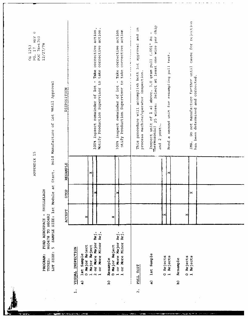
00 0 0 0-- 4 -4 -4 -4
>41 41) 4-)J 41 C-
'- r- m00 4-
-4 -,- -- 1 .-4 0 0 : 4-41( 4 1~ 4-) 4-) 0 *
(2)lc' a0) Q) Q) W 75C04~ 00 04r.
00 00 ''C 4-1 00 0 0 0 4-'
tor0r30~ r.0 -44-' 4-4 0 4 0H o
1- 0 1 00 f(a 41 41 0 0r1-1 u4
0 00 040 '4C1 W u 0004 0 .- 4 0 -4 0 Q)~ rd :3 00
In Lo 1-4 am 4)r4 CC. 44-H1 44 -k >0 a) 0
0- 0> 0> 0 CU) 0 (n04a04 0 00 4-
0 0Q) 4a 00 4-j '0 04 : C4-) U) '00 CL M o 41
r. H O) CU) '-4 Q) '00)-- -- 0. 04 4rq
E0 r 0).40 '-00a) a) -1 CN 0
$' 4- J 4 - 3 (v 4- 0 0n 4- 4
0 0' 0'0 u o 0 ---- 0 0 V(V 0 (v 0 a)ra r.0U4-J 0
C) ()0 0.0 0 14 W0 0 1 ) a04 04 P U ma 0 o 0 U)4-) I-> H , 040 (O U 0)0 4-4 4J.4 D 0 0 cq(a -P-4 d 4 )Q ,
0 oo 0o 41 0 4- 40
:J 0 - -Q) r
ra0an X
41)
41)
Q)
1-40 04>
%D
0 i 0 ___ 1 0___0
U) Ur) 9 H)r
00* 41 >0
P~04 E- Z -n -r- -r- -
0 -40 9 0 14 0-
En 4JO* 4-Or3~~n ~ 01>
.. bill, *.- 0
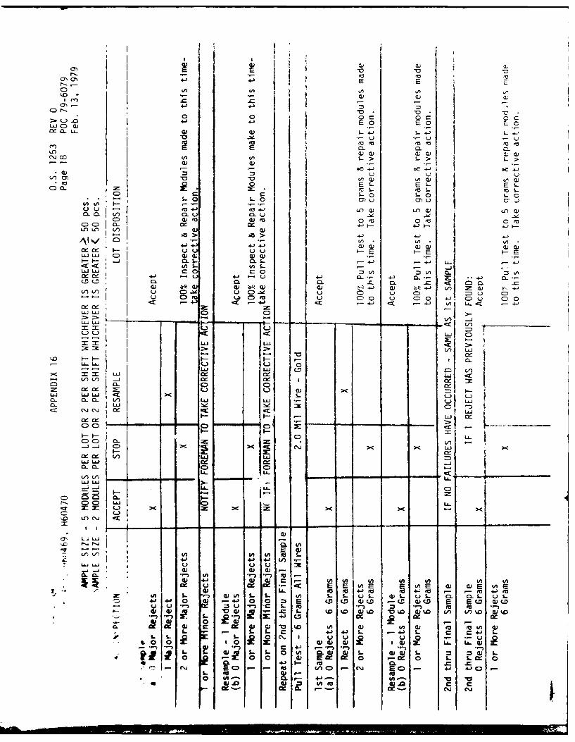
I0 0 c
E o
LO C- I
z., ~ or 4>0) Ln 0)- na
.) s- o Uov u IY U)u,
00 n
C) C) CL i wLO LO
-j CL -ca.S- 4- 4) -
= - - uC- X .4-' l-
u : W u C b ) u C) = C
4)4 0 a-LLJ C 1/
C-) L3 4)CD4 .- ) 4 4) C
U- -- 0 -_ _
LU V)
- L n __.jL0 DCw LU I±J Cxi>
a- a- - U n
~l CDLUL
CD~~ >lj> > i>
L" L)
~. C) w CD
In I
4--m 4J 4J4)i/ 1I. 0) 0.L U
4V, IA IA (-'D 4tO4 AQ 4)04)U~ 4-
ix ix cr E- E 4A4. E. E4. tL C (D- E
-L CC M~ 4-J fO4 cc 4- to4 -. 0 4-) (CI11?tn L 0A S- s-4 u S- . 0 L ca. C -uS
e- 41 -1 -U 4J 0/Zr 0C C 4 EO C- Q) CM0 E .M-)Cw . 'V 44,5- %D % o0% LUV 0 wt
S. 0 fl. r- 41 4 4n-4 . C 4J S* 0 10 R ) 2 4)E ) C
fn~~~e. C c' r, 11. fA CLcu L & S
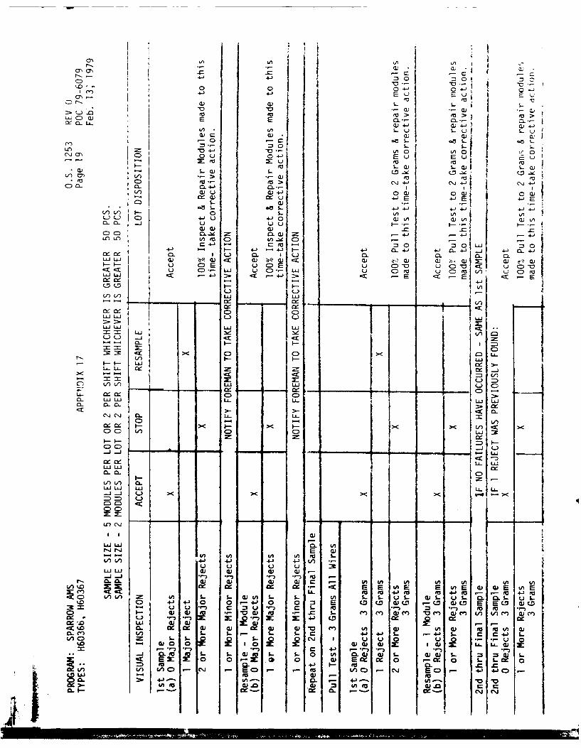
0 ~0 0
0~ CD EU E
S- L
0d *a LU L-U U
.0 L-0 $.-cNjO C O U 0 E u Ej u U
Lu L- L ) SW- LuW.
-uaiS LO 4-icC)ENCD C %CL 43 .
0 V)oS-0L()L) C 4- U 4-'0 aWIo a wI'C L'A
CDE C: in--. : La :4C4- - - toU - 0 0 Lu 0~2--) 4-) - 4-) 4-) O.4-) 4) lQ4 JJ- -*
0.~C 'a.. . I C-) Q. C-a- CLUW w4 .i) 43 (U ct 0) ZWa)c )C a) a) W m ( 3u CE u CE U CV 'v U CD U 0x u '
ctU C- LU U C)-i- LU U C'ea U C) c ) u C-L LJc -4-j E crF- I
ILr) V/) LUJ LUJ
C) CDILUJ LUJ L) LLUJ LUJ LUJ LUJ
L) J Idt14V
CD C) C< Li-Cd) - LUJ- -- LU J
- - Of
V) ) LU L -~ ~CDO. LUJ LUJ LA- - LL LUJ
C~j C\J 0. LL- Li-C 1 - Cd)
CC- >< - >< Cd) cz
F- - F-LUW LU Li..
CCD
LAl Ldl ULJ U- E 4
C)L C. I'S.
LU LU 4-3 4-3 4) 43.-
.J -j *l- . "- .1-3 *r-,) tor- a-0 (U 03) 0) 0 - UI V) LI Afl (A U
C)' %D CC. < E 0 E E (A E 4D tE UEI/I V)V ( - 1- 0 QIA .L . ( L.. L. 'u s'- 0) L -)Eus- S-EU -
CD 4-j 4-3 0 Oi4-) 0 0 E Lz( 4 _ CO. 4) CD5. ES. 0. Lo.Lu
=.. ~ )Z ,4-J CD c
m L. L. - S. L.. a 4..) 4.) S-. -4 L. C 4-) .Rn :2 R- oL- " I u u U~ X9 -9 U
W4 o-E EU W. (UE U 5-U U) LA-Q U. 433 L0)4,. EU , 0- 4-) I - .. EU 1 ., .11
1/) V)l CD (%~J - EO Q - V) EU En C) Ca E - 4.) 4.O CDto (U '-ii~
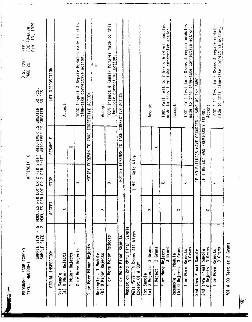
E" u Ey
I= CL 0+ )-) a
0) ; a)L
LO 1n G4LM 0)-C)0L u LuVX: Lc ) ) jul(a
Lu IL-Qj
0>- > 04-' 4-u4E u IU EU
(I -0) *0U .- r L Ead s> 4> (\4-) (\4 j4A &. . !2 . 0. n 4- (A
oL Ca -cu Cu 0C) 00)-CD L (. )4 4j4 4-'..
-nL L . ro (-) :3 4- :304-)~~ 4-) c 4 - 0 +ji 4ai CL Win-) C 4) W
CL I~o ca. Io - 0.- M:a)lU ;sR U L) a) w ) L ) ( ) l . (
Uw u CE U u CE C) u Cv u C) -0 ) mCu C -I-I-u C). - u C-- ' u C:)f u C o ~u C occ -4- cr 4r Z;- F- ~E CC E t -ELUJLU L)L) C)w = LUJ Cl LL-
LUJ LU C -
m. 0LU. cLU LU) <J 0- 1U L
zmL :9 _L C) C<
-LA- LL-. LUJ LU
_< C C) : a LUJ- V ) L. LL --
Lu LUiLLU LA-. LA- 0 0l
.: C\JC\ 0.i Q LL. LLUC Z--
LUL
V) VU LAJ
lfJ A > <>
cm in0 i
E (VL"UU (A U 0 s..
4.' + 4-' AI - I U u 3
0D .. a.. in W -cc E E 0 E E 4AE Ga GE 4AE L-x CL0 CL 4-J Ga IG- to 4-) 00 EU 4-f - 40 4J to CDl(.. C n CnU * Ai S. L. in0 L. uS- Ga L- uS UL .. UL.-1 +4) +j -) 0 0 = E D 4) mCD 0) CD E E~ (D(Dcm C\j
H ) C.) v0J u u rl7 r_ L. fa() me We A uin0- E0a () -- =-lnCAm&m+
'-4 S.. £-) V m~ Cy0 0 U a) . o%
w . **o* I- *f- +.- C- 4' C r- 4J- I- %-f043) 0) I cc 4Ga u. U en j
0D 4 0 -0 )w L. L 0lAO r- 4%J EO e- E . l.% -)E .- 4- 4'0 ,-
0w is-~ 0 CA~ 0. ' - L U) L.- i -at 5:2E 0a. Ga r= in- I-O CZ 0) C
V)1* M~ C- +-' - &L iu~ O C =\
CtY"= R A Y T H E 0 N C J Al P A N Y Os ,,, 12
"______ November 27, lq79
APPENPTX 1q, HCHM - BFDF-D PoC 79-6907
" . ISUAL T%".PFC'7TON :
]. Tnspect1 every T-7lle %r ;94.- 1,''s cioies, transistors at 100X
- All other ceatures at (1)
. Temize all repairable 'Ierects on rework sheet by serial rumlb-,
?. Fxarine: - Lot Traveler Tor proper entries-ework sheet ,itt.ached with proper entriesCopies of all inspection records
F. P1,, 'EST:
1. " achine/Onerator - Destruct Pull Test (See Appendix 13]
1. Every 4 hoursb. Use similar type or re-ect substrate assembly with eouiva'er-
chips. !7ire bond 10 w4res - substrate to chipc. Bond strenoth - 2.5 arams min. (.001 Aluminum Wire)
- Pull test to destruction
0 Faijlures - accept lot1 failure - stop. Issue TMR
Hold lots prior to failure .disposition
d. Maintain record sheet of results above.
2. Bond Strength - 1.5 qrams (Tn Process Pull Test)
a. Sample size: 2 units/lot/shiftb. Quantity: Pull test 1" wires min.
1. wire from each diode, transistor, resistor,capacitor.3 wires from post to substrateq wires fror, each IC
c. Acceptance Criteria:
- 2 samples - 0 failures accept lot
Rejection Criteria:
- 1st sample - I failure 100% pull test this unit2nd sample - 0 failures accept lot
- 1 failure Write IMR
R A Y T H E 0 N COMPANY 1261
)'44 2
April 5. 1980
L LOT ACCEPTANCE INSPECTION FOR SCREENED AND POC 80-4359TRIMMED SUBSTRATES _ -
1.0 SCOPE:
This procedure details the Inspections to be performed upon all thick
film screened substrates.
2.0 APPLICABLE DOCUMENTS:
2.1 O.S. 10072.2 O.S. 10082.3 O.S. 10092.4 O.S. 10102.5 O.S. 10182.6 O.S. 10222.7 O.S. 11282.8 Deleted per POC 70-60392.9 1. it .. ..2.10 O.S. MIL-STD-105D
3.0 EQUIPMENT:
3.1 Microscope 1O-60X Top light and backlight capability.3.2 Eyepiece with .001 micrometer disc3.3 Grounding wrist strap3.4 Digital voltmeter - HP 3440 or equivalent3.5 Multi-function plug-in HP 34443.6 Comparator 20X nikon - V-16 or equivalent3.7 Stereo microscope 10-70X Toplight capability
NOTICE:
In the event of any omissions, conflicts, ambiguities, or inconsistanciesinvolving this document and detail specification, the detail specificationshall prevail.
4.0 QUALITY IN-PROCESS CHECK - SCREENING OPERATION:
On all ARCO product using dielectric insulation layer, perform a 5 pieceQC random sample for porosity dye test (OS 1622) immediately after finalfiring of the dielectric layer. Reject the lot if the sample fails thetest.
1 '2A 3 3JA! 4I4At516 78 IS 910<281 0 1 1 5 1 Uo1_31i_0 0 2 0 0
I 16.
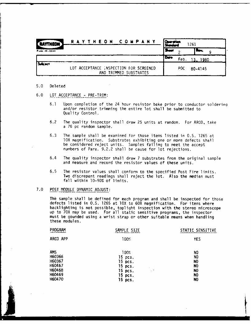
EAYO3 RA YT HEO0N CO0M P ANY 0J ~~iM 16
Po,.q 20-0044 OM2 9
_Feb. 13, 190
LOT ACCEPTANCE INSPECTION FOR SCREENED POC 80-4145AND TRIMMED SUBSTRATES
5.0 Deleted
6.0 LOT ACCEPTANCE - PRE-TRIM:
6.1 Upon completion of the 24 hour resistor bake prior to conductor solderingand/or resistor trimming the entire lot shall be submitted toQuality Control.
6.2 The quality inspector shall draw 25 units at random. For ARCO, takea 76 pc random sample.
6.3 The sample shall be examined for those items listed in O.S. 1265 atlOX magnification. Substrates exhibiting one or more defects shallbe considered reject units. Samples failing to meet the acceptnumbers of Para. 9.2.2 shall be cause for lot rejections.
6.4 The quality inspector shall draw 7 substrates from the original sampleand measure and record the resistor values of these units.
6.5 The resistor values shall conform to the specified Post Fire limits.Two discrepant readings shall reject the lot. Also the median mustfall within 10-90% of limits.
7.0 POST MODULE DYNAMIC ADJUST:
The sample shall be defined for each program and shall be inspected for thosedefects listed in O.S. 1265 at lOX to 60X magnification. For items wherebacklighting is not possible, toplight inspection with the stereo microscopeup to 70X may be used. For all static sensitive programs, the inspectormust be gounded using a wrist strap or other suitable means when handlingthese modules.
PROGRAM SAMPLE SIZE STATIC SENSITIVE
ARCO APP 10M, YES
AMS 1001; NOH60366 15 pcs. NOH60367 15 pcs. NOH60467 15 pcs. NOH60468 15 pcs. NOH60469 15 pcs. NOH60470 15 pcs. NO
jI
r~AyT-""3 R A YTH EO0N C h4 PANHY Oprtostander 12611.... ....44 Y w 2A 0~e
Data February 13, 1980
LOT ACCEPTANCE INSPECTION FOF: SCREENED 80-4145AND TRIMMED SUBSTRATES
7.G POST MODULE DYNAMIC ADJUST: (cont'd)
PROGRAM SAMPLE SIZE STATIC SENSITIVE
AMRAAM 15 pc!. NOH60454 15 pc!. NOH60455 15 pc!. NOH60457 15 Pc!. NOH60490 15 Pcs. NOH60491 15 pc!.. NOH60492 15 pc!. NOH60493 15 pc!.. NOH60494 15 pc!. NOH60495 15 pcs. NOH 60496 15 pc!. NO
8.0 Deleted per POC 70-6039
9.0 FINAL LOT ACCEPTANCE: (see Para. 13.0)
9.1 All lots of finished substrates shall be submitted to QualityControl.
RAYTHEON COMPANY 1261
I. 00443 JV 18Feb. 27, 1q79
LOT ACCEPTANCE INSPECTION FnR POC 79-6166SCREENED AND TRIMMED SUBSTRATES
9.0 FINAL LOT ACCEPTANCE: Cont.
9.2 Visual Examination (10X-60X maqnification)
9.2.1 The Quality Inspector shall draw, at randon, 25 units.
9.2.2 The sample shall he examined for those -. ect I ";te ' -O.S.1265 at 1oX to 60X magnification. Each substrate w''hone or more defects shall be considered a reject unit.Lots failinq to meet the Accept Criteris of Para. q.L).1shall be rejected.
9.2.2.1 Acceptance Number C'hart
Ind. Item Cumulat ve
Min. Defects 3 i0Major 0 n
9.3 Resistor Values:
9.3.1 The Quality Inspector shall check 25 pieces forresistor value.
9.3.2 The resistor values of each resistor on the substrateshall be measured.
9.3.3 Record the resistance values of the first five substratesand all discrepant readings noted in the remainder of thesample. Subject the first 5 substrates to heat soak at+150*+10 0 C in air for a minimum of 48 hrs. Read andrecord all resistors. Calculate R and reject if 1 or moreresistors exceed +0.5% or if resistors exceed minimum ormaximum limits. -
NOTE: For H60171A resistors R8 and R9 reject only to minimumor maximum limits criteria.
9.3.4 Substrates with one or more resistors which fail to meetthe specified resistance limits shall be considered areject unit.
9.3.5 Use Accept/Defect number of para. 9.2.2 out of toleranceresistors are a major defect. For purposes of thisinspection, out of tolerance resistors, wheter hiqh orlow, shall be considered as one type of defective.
Draw a sample of 10 substrates and check all dimensions thatapply to corrals on the applicable blueprint. No rejects allowed.
k A H N A P A NY Oper atI2
Sh t 3A Rev. 18
Dao April 5, 1980
LOT ACCEPTANCE INSPECTION FOR POC 80-4359
SCREENED AND TRIMMED SUBSTRATES
9.0 FINAL LOT ACCEPTANCE: CONT.
9.5 Conductor Adhesion Test - Solder Programs:
Two trim scrap substrates from each lot will be deliveredto the Production Assembly Foreman (Solder Programs) byQ.C. Inspector . He will have the substrates soldered andwired as described below and return them to the Q.C. Inspec-tor. The Q.C. Inspector will then evaluate the substratesas described below.
Production Soldering and Wiring:
Not later than 1 hour prior to soldering, erase the pads20-25 times to be soldered with an ink eraser #853 orequivalent and then air clean the pads.
Hand solder conductor pads to be wired per requirementsbelow in this paragraph or flow solder conductor lands onchip and wire types per O.S.1015. Solder 4 number 26tinned copper wires to conductor pads of each substrate.(See Figure 1). Use same size conductor pads where possible.Do not use exit lead oads on G.P.L. substrates. Use a maximumamount of 60/40 QQS-571 solder, Kester 1571 flux, 12 wattpretinned iron at 2450 to 270 0 C and a hot plate at 125 0 C to128°C. After soldering clean the substrates in the ultrasonicgenerator with TMC Freon for 2 minutes.
Evaluation:
Subject the substrates to 30 temperature cycles per MIL-STD-883B Method 1010.2 condition'C (-550C to +125 0 C) the exposure
time at high and low temperature will be 30 minutes. Performand record 900 C Peel Test on each joint (8 readings). Numbereach pad location on the substrate to agree with the numberof the force reading (lbs.). Record the size of each pulledpad using the microscope and reticle.* Divide the forcereading by the area of the pad to calculate the pound persquare inch reading. (PSI)*. Minimum peel strength isspecified below**. No rejects allowed after temperature cycle.
Sparrow - 360 PSI C.D.C. - 600**(See Note)G.P L - 600 PSI** Arco - 600**R. C. A. - 600 PSI
NOTE: (CDC AND RCA ONLY)
If wires, during pull test, are pulled free from thesolder pads and solder and substrate metallization areintact, then accept the sample. Do not reject.
=4 R A Y T H E 0 N C 0 h P A N Y eaw
ERAYT19-4 15
D'. January 25, 1980
LOT ACCEPTANCE INSPECTION FOR POC 80-4031SCREENED AND TRIMMED SUBSTFATES
9.0 FINAL LOT ACCEPTANCE: (cont.)
0.6 Conductor Adhesion Test - Chip and Wire Programs:
Deliver 1. scrap substratEs trom each screeninq lot to thChip and Wire Assembly area. Take 2 P/N 26380 diode chi;s(or equivalent) and procEss through a standard die attachand wire bond sequence (do not use preforms).Give the sample to the Q.C. Inspector. Parts will be testedas follows:
A. Pull test wire to 3 crams min. for 1 mil. gold wire and6 grams min. for 2 mil gold wire. Record any rejects.
B. Push test chip to 10( grams. Reject if chip shearscleanly from the concuctor or removes the gold from thesubstrate.
RAYTHEON COMPANY Y *Im
Fornn 20-0044 Sho 4 A Rev. IDe Nov. 5,
G ed LOT ACCEPTANCE INSPfCTION FORSCREENED AND TRIMEID) SIJBSTRATFS
9.0 FINAL LOT ACCEPTANCE: Cont.
* Or use appropriate chart of Appendix A.
** edioan of all readings must exceed 300 PSI.
9.- Shorts & Opens Test - Multi layer substrates. Take a 10 piecesample and test per table on applicable layout drawinq. No r, c, ta I I oed.
9.8 Short Test - Crossovers - Cn all types that have crossovers takea 10 piece sample and check all crossovers on each sample asshown below. No rejects allowed.Pi-ob oil d otPoints Czdcto
M1e1er must read overan~jeon highest ohin scale
Crossover
Q.Q Holium Leak Test (Unsealed - After Corral Attach)
The Quality Inspector shall draw a random sample from each substratelot and helium leak test per O.S. 1394. The sample size and accept/reject criteria shall be as specified below:
Table - Helium Leak Test Sample
Lot Size Sample Size * Re.:ects DispositionUp -5-7 O-U--s 25 Pcs 0 Accept Lot
I or more Reject Lot
201 Pcs or 50 Pcs. 0 Accept LotMore 1 Re-sample 50 more pieces
- Accept if 0 additional rejects- Reject if 1 or more add.
2 or more Reject lot
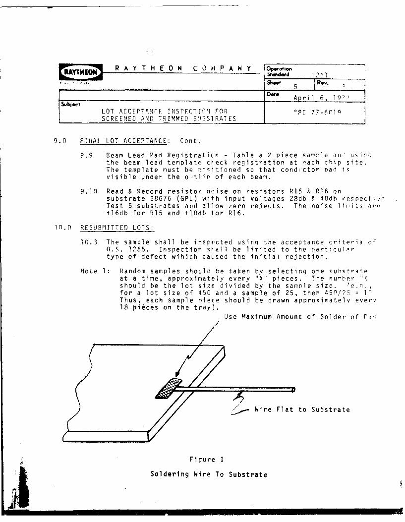
R A Y T H E 0 N C P A N Y Optio1261
F Shoo.... Rev.
Dot* April 6, 19-1Subject
LOT ACCEPTANCE INSPECTION FOR 0 PC 77-6nalSCREENED AND TRIMMED SUBSIRATES
9.0 FINAL LOT ACCEPTANCE: Cont.
9.9 Beam Lead Pad Registraticn - Table a 2 piece sam-le an' isA1-rthe beam lead template check registration at each chip site.The template must be pnsitioned so that condtctor pad iqvisible under the oltlin of each beam.
9.10 Read & Record resistor ncise on resistors R15 & R16 onsubstrate 28676 (GPL) with input voltages 28db & 40db respect ,vTest 5 substrates and allow zero rejects. The noise limits are+16db for R15 and +10db for R16.
1n.0 RESUBMITTED LOTS:
10.3 The sample shall be inspected using the acceptance criteria orO.S. 1265. Inspection shall be limited to the particulartype of defect wihich caLsed the initial rejection.
Note 1: Random samples should be taken by selecting one substrateat a time, approximately every "X pieces. The nu-her "Xshould be the lot size divided by the sample size. (e.n,for a lot size of 450 and a sample of 25, then 450/?5 = 1'Thus, each sample piece should be drawn approximately every18 pices on the tray).
Use Maximum Amount of Solder of Fpd
•/ Wire Flat to Substrate
Figure I
Soldering Wire To Substrate
iinn'u~m_
R AY T HE 0ON Cl' P ANY Optior drd 1261Show 6 0
' Mav 7. 1977
i,, LOT ACCEPTANCE INSPECTION FOR iz
SCREENED AND TRIMMED SUB',TRATES POC 77-6212
11.0 Acceptance Test for Arco Substrates
11.1 Maximum lot size to be 1000 pcs.
11.2 Test type - 10 day Humidity with bias
11.3 Sample Size - 20 tinned, cleaned and driedsubstrates
11.4 Allowable failures - 0 if short is at crossover1 if short is on surface
11.5 Conditions of Test:
Duration - 10 daysBias - 3.65 volts +.05VTemperature - 65'C±50 CHumidity - 90% RH ±5% RHFrequency of reading - 24 hrs;during weekends readings can beextended to 48 to 72 hrs.Failure criteria: leakage inexcess of lOua (100 millivoltsacross resistor). Failed unitis removed from chamber.Failure Confirmation: Air dry for24 hrs before trying to confirmfailure. Any units which "recover"or cannot be confirmed are re-turned to chamber and the test unitsare credited with a non failingcondition.
11.6 Test Method:
11.6.1 Select a minimum of 1 substrate from eachfired tray of 25 pieces before these piecesare submitted for trimming but after theyhave completed all firing stages includingtop glaze.
11.6.2 Select at random 20 pieces from the abovegroup for Humidity Test.
A P1
~A '1'0N JP A N Y operoai'-... I.. . . .. .. ... Standard 1261
S t 7 ()R, 0
May 27, 1977
LOT ACCEPTANCE INSPECTION FOR
SCREENED AND TRIMMED SUBSTRATES POC 77-6212
Test Method (Continued)
11.6.3 If the total sample size does not mae up 20pieces you may make up the total sample sizeby randomly selecting a second substrate fromany of the trays. In no case shall more thantwo substrates be selected from any one tray.
11.6.4 These substrates are to be tinned, and wired,(as per the enclosed sketch) in accordancewith the standard practice of the line atthat time. This tinning and wiring will bedone by production people on the lineand will not be done in a selected area.
11.6.5 After wiring the units will be cleaned in acc-ordance with the standard pre- pot modulecleaning operation and in a production setting.No deviation in either cleaning or drying ofthese units from standard production techni-ques will be allowed.
11.6.6 After cleaning do not touch these substrateswith your bare hands, handle the units by theirwires.
11.6.7 If a repair of the test substrate is requiredit is allowable but this unit must then berecleaned in accordance with the cleaningsequence above.
11.6.8 After drying mount the wired units to a printedcircuit test card in accordance with theenclosed sketch and submit them to the environ-mental lab for testing.
11.6.9 D notajllow the substrate lot to proceedbeyond trimming until the humidit test
12.0 Acceptance Test for Arco Substrates
12.1 Environmental Test Requirements:
Establish chamber and power supply to the limits calledout above. Apply bias to the units in accordance tothe wiring pattern in sketch No. II below. Apply thebias exactly the same at all times.
AD-A086 344 RAYTHEON CO QUINCY MASS INDUSTRIAL COMPONENTS OPERATION F/G 9/1MANUFACTURING METHODS AND TECHNOLOGY ENGINEERING (MM AND TE) PR_-ETC(U)APR 80 R M ZILBERSTEIN DAABO07 TA C-8110
UNCLASSIFIED DELET-TR-76-8119 F _VOL_2 NL
1.8
1.j 25 1111.4 1111.6
MICROCOPY Ni SOL LIIN 11SI CHIAR I
R A Y T H E O N C 14 P A N Y Olai05rndod 1261Shoot 8 1 Rev. 0,
fl _t May 27, 1977LOT ACCEPTANCE INSPECTION FOR
SCREENED AND TRIMMED SUBSTRATES POC 77-6212
Environmental Test Requirements (continued)
12.2 Read every 24 hours ±1 hour. Exception to this rule isgranted during weekend operation as quoted above.
12.3 Avoid touching the units with your bare hands, Hang theunits in the chamber, do not stack the units on top ofone another. Make every effort to keep units from touch-ing.
12.4 Units which show any leakage are to be noted in the log;however, a unit is not considered to have failed untilit exhibits 120+ millivolts leakage.
12.5 Remove failed units from the test chamber and allow themto air dry for 24 ±2 hours before any confirmation test-ing is to be performed. During weekend operation whentest confirmation cannot be performed within a 30 hourperiod, the failed units are to be left in the chamberuntil the time sequence is such that this analysis canbe performed.
12.6 Deviation of the test confirmation will be allowed underspecial circumstances, in any case if confirmation cannotbe obtained within (30) thirty hours return the suspectunit to the humidity chamber until such time as conditionsallow control testing.
12.7 Q.C. Test Engineer:
12.7.1 Avoid any sudden application of power to thesedevices when trying to confirm the humiditytest results.
12.7.2 Apply test prober through a resistive load soas not to burn out or fuze any probable short inthe unit.
12.7.3 If the failure cannot be confirmed return theunit to the humidity chamber and continue thetest as having no failure history.
12.7-.4 If the failure is confirmed to a surface area(between conductors) two or more failures man-date one of the following:
12.7.5 Define whether the failure is caused by acosmetic problem (eg) misalignment, scratchedmetalization etc. If this is the failure mode
RAY N R A Y H ON C 0 P4 P A N Y S.mat= 1261_______ ______ 9__ __ Rev.
.Ober~her 12. 1977LOT ACCEPTANCE INSPECTION FOR ?W 77-6391
SCREENED AND TRIMMED SUBSTRATES
Environmental Test Requirements (continued)
a 100% visual evaluation of the entire lot isto be carried out. The reject units are to beeliminated and a retest is to be performedon the residual of the lot.
12.7.6 If the defect is caused by surface contamin-ation (eg) flux or fingerprints, remove thetest pieces from the chamber, reclean inaccordance with the cleaning conditions describedabove and resubmit the units to the test sequence,starting at the time whe-n the failure occurred.
12.8 If the failure is confirmed to a cross over area, onefailure rejects the lot and it is put on hold. A secondsubmittal of samples will be allowed, if a subsequentfailure occurs the total lot is rejected and scrapped.If no subsequent failures develop the lot is given aqualified release and carefully monitored throughoutthe line. Secondary failures in this lot will necessi-tate removal of the entire lot from the line.
13.0 Lot Packaging
Inspect each lot prior to delivery to stores. The entire lot mustgo into stores and remain in stores in covered containers.
14.0 PRE-inspection Step
Check that all substrates are properly wired prior to submittal toHumidity Evaluation.
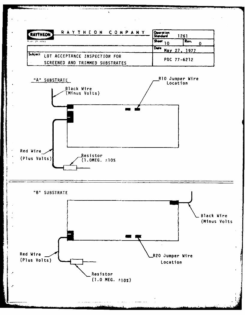
&________-_nu _ R_ A YT_ H E_0_H C_0______A_____n 160
____ ___ ____ ___ ___ ____ ___ ___ ____ ___ ___ may_27,_1977
Sibgc' LOT ACCEPTANCE INSPECTION FOR POC 77-6212SCREENEDANDTRIMMEDSUBSTRATES_____________
"B" SUBSTRATER1 JuprW e
BBlack Wire_Mnu Vo(lts)Vlt
Red WireR2 JuprWej Pu Vls (1. MEG. 1 % )
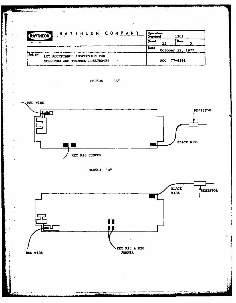
R AY T HEO0N CO01MP ANY y watinRAYTHE 1261,1 0
i .... . ... :Show 11 Rev. 0
7 . . ... Doe October 12, 1977
LOT ACCEPTANCE INSPECTION FOR
SCREENED AND TRIMMED SUBSTRATES POC 77-6391
H60504 "A"
RED WIRE
SISTOR
] BLACK WIRESI7
KEY RI0 JUMPER
H60504 "B"
WIRE
KEY R15 & R20RED WIRE JUMPER
-.bok&
P AY TH F0 N 0 PA 1263 .
1 1 1_______Dec. 20, 1978
QUALITY INSPECTION OF DIE ATTACH POC 78-6696OPERATION _
1.0 SCOPE:
This instruction details the inspection methods to be employed in
performing In-Process Inspection of the Die Attach Operation.
2.0 APPLICABLE DOCUMENTS:
2.1 O.S. 1265
3.0 EQUIPMENT:
3.1 Microscope B+L Stereozoom with coaxial illuminator or equivalent.
4.0 LOT INSPECTION:
4.1 Upon completion of the die attach operation the entire lot shall besubmitted to Quality Control for 100% visual inspection and sampletested for die adherence (push test).
4.2 The sample shall be inspected using the acceptance criteria ofO.S. 1265.* The die attach operation shall be inspected at 30X to50X magnification. Chip damage and defects shall be inspected at75X to lOOX magnification.
4.3 Lots failing to meet N=5, C=O for push test shall be rejected for100% push testing.
5.0 PROCESS AUDIT:
5.1 Twice each day, a sample of 5 pieces will be taken from each dieattach operation and inspected per O.S. 1265* for visual and pushtest criteria. Information of defective units will be immediatelytaken to Production Foreman and Process Engineer.
5.2 Push Test:
N = 5, C = 0
* For Arco and Medrad die attach, use MIL-STD-883, Method 2010, Condition Afor IC's (cMos) and MIL-STD-750B, Method 2072 for transistors and diodes.Use magnification specified per applicable sections of 883 and 750.
IL lIION R A Y T H E 0 N C 0 Mt P A N Y 1276
Fon 20-0044 1 Re. 2IDefe July 8, 197,5
CENTRIFUGING HYBRID CIRCUITS lPOC 75-6181
1.0 PURPOSE:
1.1 To specify a method of Centrifuging Hybrid Circuits to pullloose poor wire bonds and semiconductor chips.
2.0 SAFETY:
2.1 Normal precautions are to be observed.
3.0 EQUIPMENT AND TOOLS:
3.1 International Centrifuge size 2 Model V or equivalent.
3.2 Electronic Counter #523D or equivalent.
3.3 Centrifuge Fixture #2518 or equivalent.
3.4 Damon IEC HT
4.0 MATERIALS AND SUPPLIES:
4.1 Hybrid Circuits
5.0 REQUIREMENTS:
5.1 All circuits to be Centrifuged in the Yl DIRECTION,
6.0 PROCESS PROCEDURE: (International Centrifuge at Fixture #2518)
6.1 Place the circuits to be Centrifuged in the ftxture with topof the circuit facing the outside of the fixture; this is theYl DIRECTION. Make sure the fixture is balanced by evenlyspacing circutts around drum.
6.2 Place the cover on the fixture and close centrifuge door.
6.3 Check the Centrifuge Chart, Table I, for the G level at whichyou are going to Centrifuge the circuits. Centrifuge level isspecified on the applicable Flow Charts.
6.4 Turn on the Centrifuge powerstat to approximately 4 amp. untilthe Centrifuge Electronic Counter starts, then increase to 10until the counter reaches the G level, Maintain this G levelfor 1 mtnute minimum.
6.5 When the counter reaches the G level turn off the power, and
apply pressure to the brake until Centrifuge stops.
6.6 Open Centrifuge cover and remove circuits.
6.7 Repeat for additional circuits. 1 2 3
211 i
R A Y THEON C0MPAN Y Ow 1276
Vann 20-0044 see 2 JR . I
Dot* June 24, 1975
i CENTRIFUGING HYBRID CIRCUITS POC 75-6153
___I
7.0 PROCESS PROCEDURE: (Damon IEC HT)
7.1 Place the circuits to be centrifuged in the fixture withtop of the circuit facing the outside of the fixture, thisis the Y1 direction. Make sure the fixture Is balanced(load evenly di'stributed).
7.2 Place the cover on the fixture and close centrifuge door,
7,3 Check the flow chart for the G level at which to centrifugethe circuits.
7.4 Place speed control to zero,
7.5 Place power On/Off switch to *ON WITHOUT TIMER4.
7.6 Place Brake/Run switch to NRUN4 ,
7.7 Place Amp/RPM switch to "RPM"l,.
7.8 Turn up speed control slowly.
CAUTION: O NOT EXCEED 9 AMPS ON THE AMP METER AT ANY TIME
7.9 Stop speed control at the desired WG" level indicated on thecalibration chart on the test machine, Maintain this levelfor one (1) minute.
7.10 After 1 minute turn speed control to zero.
7.11 Place Brake/Run switch to "BRAKE".
7.12 Turn speed control up slowly until Amp meter reads 2.5 amps,
7.13 When RPM meter reads 1, immediately turn speed control to
zero.
7.14 Return Brake/Run switch to run.
7.15 Open centrifuge and remove circuits. Check for broken ordamaged circuits.
7.16 Repeat procedure on additional circuits.
8.0 MAINTENANCE:
8.1 Check belt each week on International and adjust if needed.
Ponm 20-0044 SUw 3 Rev.D* June 24, 1975
C E T FJ 1'14. 'Y R DC CITSC' 75-615/y
CE N I t CE CA.TTABE I
>r.eiuencv Counter at .arious Levels
'C.P.S. CCL'NI'Ei READINC1
*'Level 3"' adius 2 15/16" 3 3/16 RZadiusCeramic .,adius Letal With No
_________Insert x.nsert _nsert
10357.3 C.? .,S. 57.9 C.P.S. S7
t5,000 12 '8 130 124
5I 6, 140 "142 132
'7, 0 10 152 1S4 147
S,03162 163 152
9,000 172. 174 167
1c,O0C 181 1S3 175
I15,0On0 222 225 214
20,000 257 25c- 247
25,000o 28190 278
30,000 314 318 3015
7or Other Radii C. Iculate
2, .3 .12,7 7
------
__ __ ___,__ __ __ __ __ __-_ ___o__ __ __ __ _ 1 ]Re'. 15
SFebtrary 14, 1980
TEMPERATURE CYCLING HYBRID CIRCUITS POC 80-4169
1.0 PURPOSE:
1.1 To specify a method of temperature cycling Hybrid Circuits to detectdefects in Pack and Sealing.
2.0 SAFETY:
2.1 Normal precautions are to be observed.
3.0 EQUIPMENT AND TOOLS:
3.1 Standard Temp-Cycle Model #LHTS/3F3 or equivalent.
4.0 MATERIALS AND SUPPLIES:
4.1 Hybrid Circuit
4.2 Tray
5.0 REQUIREMENTS:
5.1 All circuits to be temperature cycled as specified in Para. 6.0and MIL-STD-883, Method 1010.
6.0 PROCESS PROCEDURE:
6.1 Set the number of cycle, temperatures and times per Table I for thecircuit to be temperature cycled.
6.2 Place the tray of circuit in the temperature cycle making surecircuits and tray are secure.
6.3 Close the doors making sure they are closed tight as the doors havean interlock.
6.4 To start the cycle press the white button on the cycle Shut Off andthen the cold first button.
6.5 Machine will automatic cycle through the Hot and Cold chamber.
6.6 At the end of the cycle the machine will automatically turn off, soremove the tray.
6.7 Repeat the above for additional circuits to be temperature cycled.
1.5 0 5 4 -4.,
R _A YT H E 0 N C 0 M P A N Y 0 29
.. ,,R e 2 Re . 0
DO* Feb. 21, 1972subiet TEMPERATURE CYCLING HYBRID CIRCUITS POC 72-6013
7.0 INSPECTION:
7.1 Inspect circuits for damaged leads, cracked packages, etc.
8.0 MAINTENANCE:
8.1 Calibrate the Hot and Cold chambers each month.
8.2 Check the Travel between the Hot and Cold chamber each month.
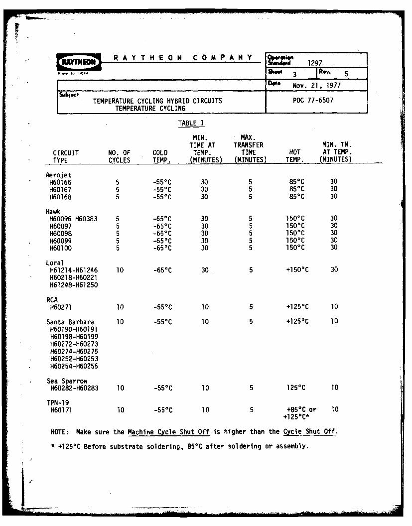
Nov. 21, 1977
TEMPERATURE CYCLING HYBRID CIRCUITS POC 77-6507
TABLE I
MIN. MAX.TIME AT TRANSFER MIN. TM.
CIRCUIT NO. OF COLD TEMP. TIME HOT AT TEMP.TYPE CYCLES TEMP. (MINUTES)- -(MINUTES) TEMP. (MINUTES)
AerojetH60166 5 -550C 30 5 850C 30H60167 5 -550C 30 5 850C 30H60168 5 -550C 30 5 850C 30
HawkH60096 H60383 5 -650C 30 5 1500C 30H60097 5 -650C 30 5 1500C 30H60098 5 -650C 30 5 1500C 30
* H60099 5 -650C 30 5 1500% 30H60100 5 -650C 30 5 1500C 30
* LoralH61214-H61246 10 -650C 30 5 +1500C 30H60218-H60221H61248-H61 250
RCAH60271 10 -550C 10 5 +1250C 10
Santa Barbara 10 -550C 10 5 +1250C 10H601 90-H601 91H601 98-H601 99H60272-H60273H60274-H60275
* H60252-H60253* H60254-H60255
Sea SparrowH60282-H60283 10 -550C 10 5 1250C 10
TPN-19H60171 10 -550C 10 5 +850C or 10
+1 250C*
NOTE: Make sure the Machine Cycle Shut Off is higher than the Cycle Shut Off.
*+1250C Before substrate soldering, 85*C after soldering or assembly.
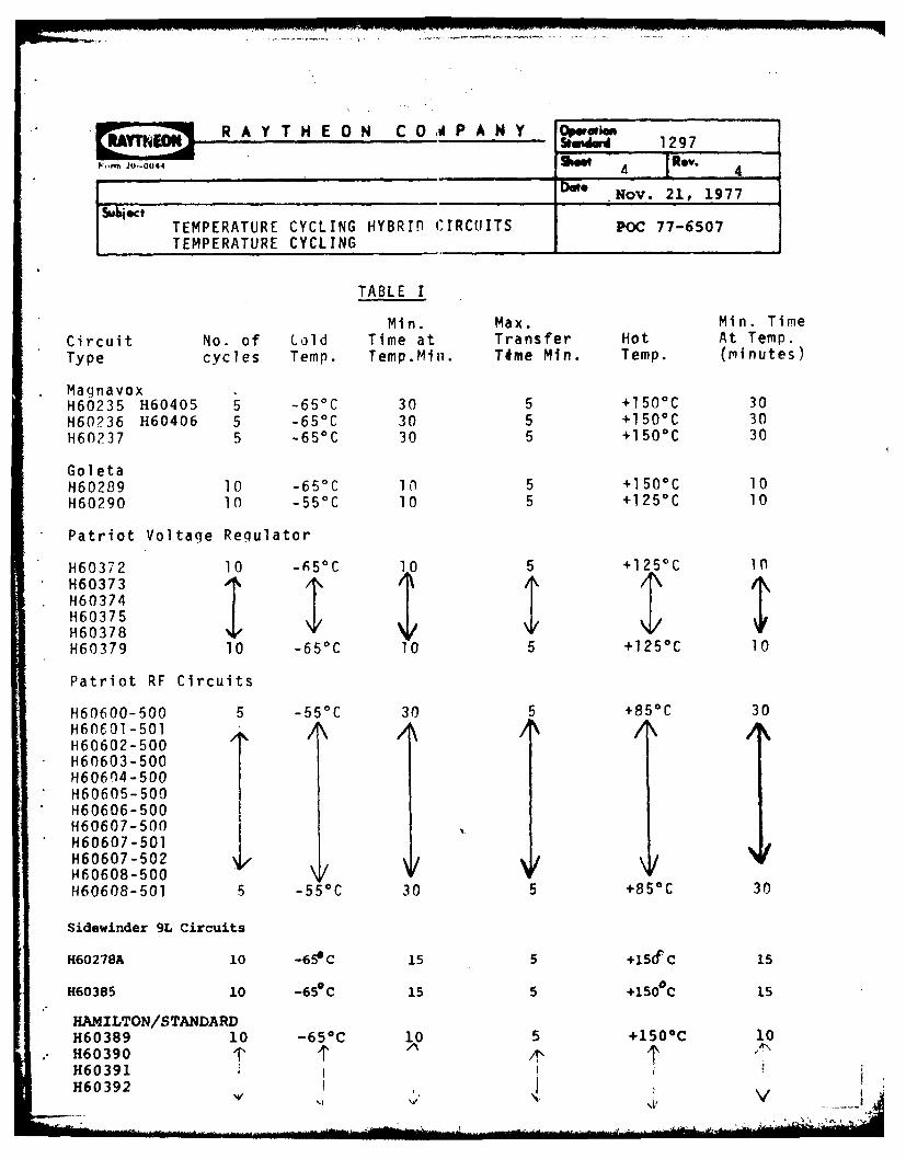
'" -S~w 1297 ,
F-m20-04 sw 4 Rev. 4.... Nov. 21, 1977
&~ij tTEMPERATURE CYCLING HYBRIO CIRCUITS POC 77-6507TEMPERATURE CYCLING
TABLE I
Min. Max. Min. TimeCircuit No. of Cold Time at Transfer Hot At Temp.Type cycles Temp. Temp.Min. T#me Min. Temp. (minutes)
MagnavoxH60235 H60405 5 -65 0 C 30 5 +150 0 C 30H60?36 H60406 5 -650 C 30 5 +150 0 C 30H60237 5 -650C 30 5 +150 0C 30
GoletaH60289 10 -650 C 10 5 +150 0 C 10H60290 10 -550 C 10 5 +125 0 C 10
Patriot Voltage Regulator
H6037 2 10H6050C010H03751205 ° C
*H60373H60374ITITCS H60378
H60379 10 -650 C 10 5 +125 0 C 10
Patriot RF Circuits
H60600-500 5 -55°C 30 5 +850C 30H60601-501 AH60602-500H60603-500H60604-500H60605-500H60606-500H60607-500H60607-501H60607-502 / /
H60608-500 \H60608-501 5 -55*C 30 5 +850 C 30
Sidewinder 9L Circuits
H60278A 10 -65C 15 5 +15(fC 15
H60385 10 -65C 15 5 +150C 15
HAMILTON/STANDARDH60389 10 -650C 10 5 +1500C 10H60390 T A ./\H60391H60392 I
'VW"
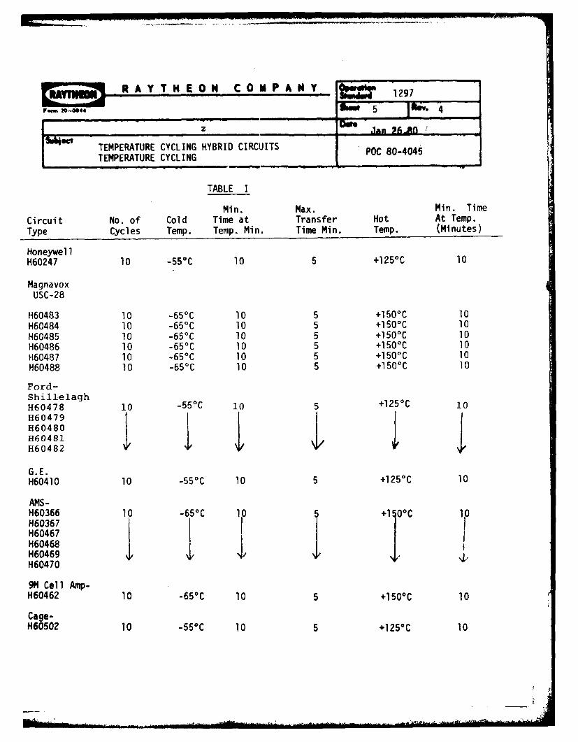
N C 0 M P A N Y5 1297Sm" 5 Ifti 4
z Je. Jan 2 6A
..- jIe TEMPERATURE CYCLING HYBRID CIRCUITS poc 80-4045TEMPERATURE CYCLING
80
TABLE I
Min. Max. Min. TimeCircuit No. of Cold Time at Transfer Hot At Temp.Type Cycles Temp. Temp. Min. Time Min. Temp. (Minutes)
HoneywellH60247 10 -550C 10 5 +125°C 10
MagnavoxUSC-28
H60483 10 -650C 10 5 +1500C 10H60484 10 -650C 10 5 +1500C 10H60485 10 -650C 10 5 +1500C 10H60486 10 -650C 10 5 +150 0C 10H60487 10 -65C 10 5 +1500C 10H60488 10 -650C 10 5 +150°C 10
Ford-ShillelaghH60478 10 -55°C 10 5 +125°C 10
H60479JIH60480
H60481H60482
G.E.H60410 10 -550C 10 5 +125 0C 10
AMS-H460366 10 -650C 10 +1100C 10H60367IIH60467 I I IH60469 'P4
H60470
9M Cell Amp-H60462 10 -650C 10 5 +150 0C 10
Cage-H60502 10 -550C 10 5 +125 0 C 10
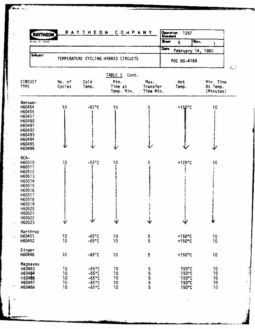
RAY___._q OPwatson 1297____00____sIow 6 Rev.0. February 14, 1980
Subject TEMPERATURE CYCLING HYBRID CIRCUITS POC 80-4169 J
TABLE I Cont.
CIRCUIT No. of Cold Min. Max. Hot Min. TimeTYPE Cycles Temp. Time at Transfer Temp. At Temp.
Temp. Min. Time Min. (Minutes)
Amraam-H60454 10 -65 0 C 10 5 +1 )C 10860455H60457H60490H60491 IH60492H60493H60494H60495 , &H60496 /
RCA-H60510 1 -550C 10 5 +125 0C 10H60511 'H60512H60513 | iH60514 1H60515H60516 JH60517H60518H60519
H60520860521H60522H60523 //
NorthropH60451 10 -650C 10 5 +150 0C 10H60452 10 -650C 10 5 +150 0C 10
SingerH60446 10 -650C 10 5 +150 0 C 10
MagnavoxH60483 10 -65°C 10 5 1500C 10H60484 10 -650C 10 5 150 0C 10H60486 10 -650C 10 5 1500C 10H60487 10 -650C 10 5 1500C 10H60488 10 -650C 10 5 1500C 10
I".
ON IL"Y385o m 2- 044 g h n e . 5
I DIN September 21, 1978
SCLEANING SUBSTRATS PRIOR TO DIE ATTACH ANDTER DYNAMIC ADJUST FOR HAWK (ALL TYPES TPN-19, APP POC 78-6515
1.0 PURPOSE:
1.1 To specify a method of cleaning substrates before die attach and afterdynamic trim to remove trimming and other foreign particles.
2.0 SAFETY:
2.1 Normal precautions are to be observed for handling cleaning solutions.
2.2 Operator is to wear finger cots.
3.0 EQUIPMENT AND TOOLS:
3.1 Ink Earaser #8533.2 Pyrex Beaker3.3 Cobehn Spray Equipment #B6/8/9 1/2/2AAY3.4 Grounding Fixture3.5 Clean Metal Trays3.6 Exhaust Hood3.7 Oven (1250 C)3.8 Hot plate 125°F + 10°F3.9 Tweezers3.10 Metal hood for hot plate3.11 Stainless Steel Basket3.12 Ultrasonic Cleaner3.13 Nitrogen Storage Cabinet
4.0 MATERIALS AND SUPPLIES:
4.1 Cobehn4.2 Isopropyl alcohol (electronic or Mos grade)
4.3 Conductive elastomatic #40-XX-1010-1212 or equivalent.4.4 Finger cots4.5 Acetone - electronic or Mos grade4.6 Trichloroethylene - electronic or Mos grade4.7 Nitrogen blow line
5.0 REQUIREMENTS:
5.1 Substrates and attached components must be free of all foreign matter.
5 4 2 0
R A Y T H E-O N C 0 M P A N Y 1385
2 . . e, 4
_"_September 21, 1978elCLEANING SUBSTRATES PRIOR TO DIE ATPACH AND AFTER
DYNAMIC ADJUST FOR HAWK (ALL TYPES) TPN-L9 AND APP 78-6516
6.0 PROCESS PROCEDURE:
6.1 Prior to Die Attach Only:
6.1.1 Abrade gold and (on TPN-19 and APP only) platinum-gold conductorswith ink eraser until uniformly shiny. Pay particularattention to corners and along inside edges near corral.
6.1.2 Blow off substrates with nitrogen to remove eraser particles.
6.1.3 Place the units in a basket. Place the basket in the glassbeaker filled with Trichloroethylene.
6.1.4 Place the beaker in ultrasonic cleaner and clean for 3 +minutes.
6.1.5 Lift the basket and rinse the modules in the basket using freshTrichloroethylene.
6.1.6 Repeat above 6.1.3, 6.1.4 and 6.1.5 using Acetone.
6.1.7 Repeat above 6.1.3, 6.1.4 and 6.1.5 using Isopropanol.
6.1.8 Blow dry the units with Nitrogen gas.
6.1.9 Place the units on a tray covered with lint free paper.
6.1.10 Dry the units in an oven at 125 C + 5°C for hr + 5 min.
6.1.11 Store the trays in a closed cabinet filled with Nitrogen until
ready for use.
6.2 DYNAMIC ADJUST (HAWK AND TPN-19 ONLY)
NOTE: It is important that the following procedure is strictly adhered to whencleaning units after dynamic adjust.
6.2.1 Check that air pressure at Cobehn unit is 40 PSI.
6.2.2 Check that temperature gauge reads between 90 C and 1100C.
6.2.3 Check that ground lead of fixture is secure.
6..2.4 Put on finger cots before handling modules.
6.2.5 Load one or two modules into fixture as shown in Figure 1........
R A Y T H E 0 N C 0 4 P A N Y 1385
•om 20-0044 "60 3 2
MoeeCLEANING SUBSTRATES PRIOR TO DIE ATTACH AND POC 78-6515
AFTER DYNAMIC ADJUST FOR HAWK (ALL TYPES) TPN-19, APP
6.2 DYNAMIC ADJUST (HAWK AND TPN-19 ONLY Cont.
6.2.6 Hold fixture with modules facing spray nozzle approximately 2inches from the nozzle. Spray units with dry air for approxi-mately 10 seconds.
6.2.7 Spray with Cobehn by depressing foot pedal, holding fixture nocloser than 2 inches from nozzle and no farther than 2.5 inchesfrom nozzle. Spray for 3.5 seconds moving fixture as necessaryto direct spray over the entire surface of exposed module ormodules.
6.2.8 Release foot pedal and spray units with dry air for approximately8 seconds.
6.2.9 Remove modules from fixture and immerse in isopropyl alcohol,swish around once and place in hot plate for 2 to 5 minutes.Place on a clean metal tray, face down.
6.2.10 Continue preceeding steps on all modules.
6.2.11 Store in a dry nitrogen cabinet until the next operation.
7.0 INSPECTION:
7.1 Inspect under a 40X microscope for trimming particles and other foreignmatter.
8.0 MAINTENANCE:
8.1 Check Cobehn heater temperature and air pressure daily and during use.
8.2 If an automatic timer is in use for regulating time cycles of spray,check times of cycles daily.
I
Rot A004 Y TRE0. 0 M-
____ ___ ___ ___ ____ ___ ___ ___ ____ ___ ___ _ ~ Dec. 19, 1974
SAO"s ('IEIANING SUBSTRATES PRIOR TO DIE ATTACH POC 74-6341ANi) AFTER DYNMIC ADJUST FOR HAWK (all types)LAND TPN-19____________
Figure I
IWO-"'
R A Y T H E 0 N C 0 M P A N Y _aRA TH ON CO PA Y 1394
Ponm 20-0044 5 1 ROv. 2
D4@e March 3, 1980
HIE. IUM I.EAK TIST AFTER CORRAL ATTACII POC 80-4219
-
1 . 0 PURPOSE:
To specify a method of fine leak testing Hermetically corral sealedIlbrid Circuits using Hlelium leak detector.
2. 0 SAFETY:
2.1 Normal precautions are to be observed.
3.0 EQU I PMI'N'1 ANI) TOOLS:
3. 1 Hel ium leak detector VEECO MIS-12 or equivalent.
3.2 tOven 0-20 0°( Blue \#OX"-490A-1 or equivalent.
3.3 Ultraviolet l-amp #B-100A or equivalent.
4 .0 MATIERIALS AND SIUPPLIES:
4.1 leI iuin
4.2 Hlybrid Circuits
4 . 3 Vacuum Grease - Celvacene Hleavy
4.4 Axothene VG (Electronic Grade)4.5 Acetone (Electronic Grade)
4.0 Iso-Propyl Alcohol (Electronic Grade)
5. 0 RIQLIJI RE tILNTS:
5.1 No Hlelium leaks.
0.0 PROCESS PROCHlURL:
6.1 ilelium leak detector to be calibrated before using.
t.2 Push the vent switch, and then place circuit on rubber "ixturewith a small amount of vacuum grease.
13 4 **44-'1 i2 0, |
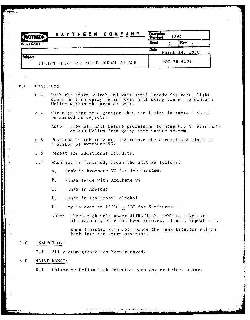
PAA TH O..C MP N ,MoM~ 1394 .-
en 20-0044 9 2 1 RevI Il lt 'Date MA rch 14- 1978
111.1 I UM I.LAK TST FTE'riR CORLRAI TACH POC 78-6105
0.0 Continued
0.3 Push the start switch and wait until (ready for test) lightcomes on then spray Ieliun over unit using funnel to containHelium within the area of unit.
b.4 Circuits that read greater than the limits in Table I shallbe marked as rejects.
Note: Blow off unit before proceeding to Step 6.5 to eliminateexcess Helium from going into vacuum system.
0.5 Push the switch to vent, and remove the circuit and place ina beaker of Axothene VG.
0.0 Repeat for additional circuits.
0.7 When lot is finished, clean the unit as follows:
A. Soak in Axothene VG for 3-5 minutes.
B. Rinse twice with Axothene VG
C. Rinse in Acetone
D. Rinse in Iso-propyl Alcohol
E. Dry in oven at 125'C + 5C for 5 minutes.
Note: Check each unit under ULTRAVIOLET LAMP to make sureall vacuum grease has been removed, if not, repeat o.
When finished with lot, place the Leak Detector switchback into the start position.
7.0 I NSPECTION:
7.1 All vacuum grease has been removed.
8.0 MAINTENANCE:
8.1 Calibrate Helium leak detector each day or before using.
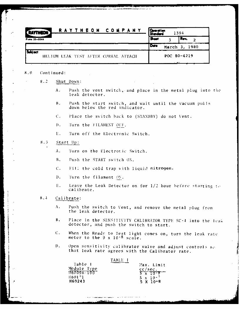
h O R A Y T H E 0 N C 0 P A N Y 0 139
Poem 20-0044 Show 3 Rv. 2
I March 3, 1980
HE11l LIM IAK I'T .\FT:1IFR CORRA l AI'ACII POC 80-4219
8.0 Cont inued:
8.2 Shut Down:
A. Push the vent switcl., and place in the metal plug into theleak detector.
B. Push the start switch, and wait until the vacuum pullsdown below the red indicator.
C. Place the switch back to (STANDBY) do not Vent.
I). Turn the FILAMENT OFF.
1. Turn off the Electronic Switch.
8.3 Start Up:
A. Turn on the Electronic Switch.
B. Push the START switch ON.
C. Fill the cold trap %,ith liquiL nitrogen.
D. Turn the filament OX.
F. Leave the Leak Detector on for 1/2 hour before starting tocalibrate.
8.4 Calibrate:
A. Push the switch to Vent, and remove the metal plug fromthe leak detector.
B. Place in the SENSITIVITY CALIBRATOR TYPE SC-4 into the leakdetector, and push the switch to start.
C. When the Ready to Test light comes on, turn the leak ratemeter to the 9 x 10⁻⁸ scale.
1). Open sensitivity calibrator valve and adjust controls sothat leak rate agrees with the Calibrator rate.
TABLE ITable I Max. Limit
Module TIvee cc/sec.1160096-M0 5 x 10-811601"1 ; x 10- 7
F160243 5 X 10⁻⁸
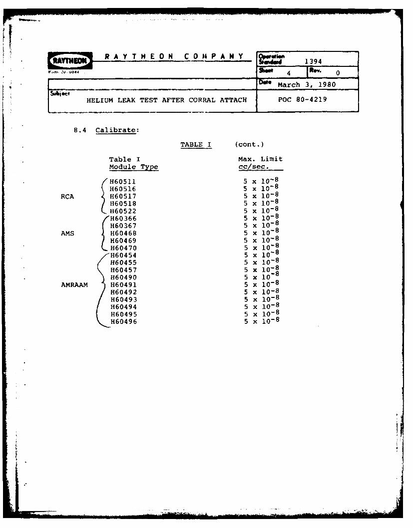
rl-V R AY T HE ON C 0 14 P A N Y 0 1394
... ' 4 to"
March 3, 1980Su j ct
HELIUM LEAK TEST AFTER CORRAL ATTACH POC 80-4219
8.4 Calibrate:
TABLE I (cont.)
Table I Max. LimitModule Type cc/sec.
H60511 5 x 10⁻⁸H60516 5 x 10- 8
RCA H60517 5 x 10- 8
H60518 5 x 10-81160522 5 x 10⁻⁸
/'H60366 5 x 10- 8
H60367 5 x 10⁻⁸AMS H60468 5 x 10- 8
/H60469 5 x 10-81. H60470 5 x 10⁻⁸
H60454 5 x 10⁻⁸
H60455 5 x 10⁻⁸
H60457 5 x 10⁻⁸H60490 5 x10-
AMRAAM H60491 5 x 10⁻⁸H60492 5 x 10⁻⁸H60493 5 x 10⁻⁸H60494 5 x 10⁻⁸H60495 5 x 10⁻⁸H60496 5 x 10⁻⁸
rRAT4" RAYTHEON COMPANY
n-wi.. ,Y T ON COP N Y470Fon 20-0044 1 JR&ev 3
DO October 22, 1979&Nd IN-PROCESS INSPECTION OF THE THICK FILM (oc 79-6775
SCREENING AND CORRAL ATTACH OPERATIONS
1.0 PURPOSE:
This standard is to provide control for screening and corral attachoperations using visual criteria.
2.0 EQUIPMENT:
lOX to 30X sterozoom microscope with provision for transmitted light.
3.0 DOCUMENTATION:
O.S. 1265Applicable screened substrate drawingApplicable lot travelerData sheet of Appendix A
4.0 FREQUENCY OF INSPECTION:
At approximately 8:30 A.M. - 11:00 A.M. and 2:30 P.M.
5.0 SAMPLE SIZE:
Sample s4Le shall be five (5) units for all inspections.
6.0 PROC:DURE:
6.1 The inspector shall draw the required sample after thescreening and drying sequence, and for corrals after thecorral attach firing sequence. The inspector shall alsocheck other start-up parameters as detailed in paragraph7.2 and record these results on the data sheet of sheet 3.
6.2 Using the steromicroscope, the inspector shall inspect thesample to the criteria of O.S. 1265 and record all data asdetailed on the data sheet of Appendix A. The inspectioncriteria of O.S. 1265 is modified for this inspection tothe extent detailed in paragraph 7.0.
6.3 Samples with one or more defects shall be cause for rejection.
6.3.1 If one defect is found the cognizant supervisor shallbe notified.
6.3.2 If two or more defects are found the inspector shallnotify the cognizant supervisor and the process shutdown until an acceptable sample is obtained.
1 2 3
3 2 0
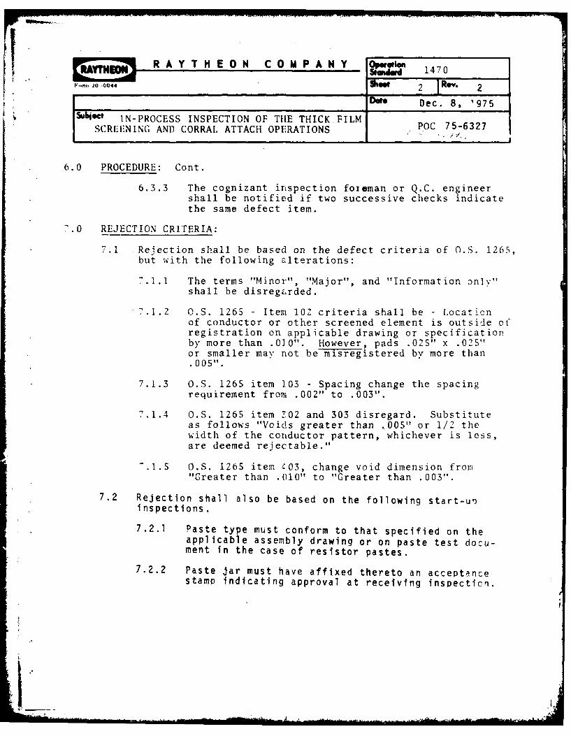
rRATHR AY TH EO0N COM P A NY 1470
S..... 20 -0044 shw 2 Rev. 2
Doe. Dec. 8, 1975
Iabi.t IN-PROCESS INSPECTION OF THE THICK FILM
SCREENING AND CORRAL ATTACH OPERATIONS POC 75-6327
6.0 PROCEDURE: Cont.
6.3.3 The cognizant inspection foieman or Q.C. engineershall be notified if two successive checks indicatethe same defect item.
.0 REJECTION CRITERIA:
7.1 Rejection shall be based on the defect criteria of O.S. 1265,but with the following alterations:
7.1.1 The terms "Minor", "Major", and "Information only"shall be disregarded.
7.1.2 0.S. 1265 - Item 102 criteria shall be - Locationof conductor or other screened element is outside ofregistration on applicable drawing or specificationby more than .010". However, pads .025" x .025"or smaller may not be misregistered by more than.005".
7.1.3 O.S. 1265 item .03 - Spacing change the spacingrequirement from .002" to .003".
7.1.4 O.S. 1265 item 302 and 303 disregard. Substituteas follows "Voids greater than .005" or 1/2 thewidth of the conductor pattern, whichever is less,are deemed rejectable."
>.1.S O.S. 1265 item 403, change void dimension from"Greater than .010" to "Greater than .003".
7.2 Rejection shall also be based on the following start-uninspections.
7.2.1 Paste type must conform to that specified on theapplicable assembly drawing or on paste test docu-ment in the case of resistor pastes.
7.2.2 Paste jar must have affixed thereto an acceptancestamp indicating approval at receiving inspection.
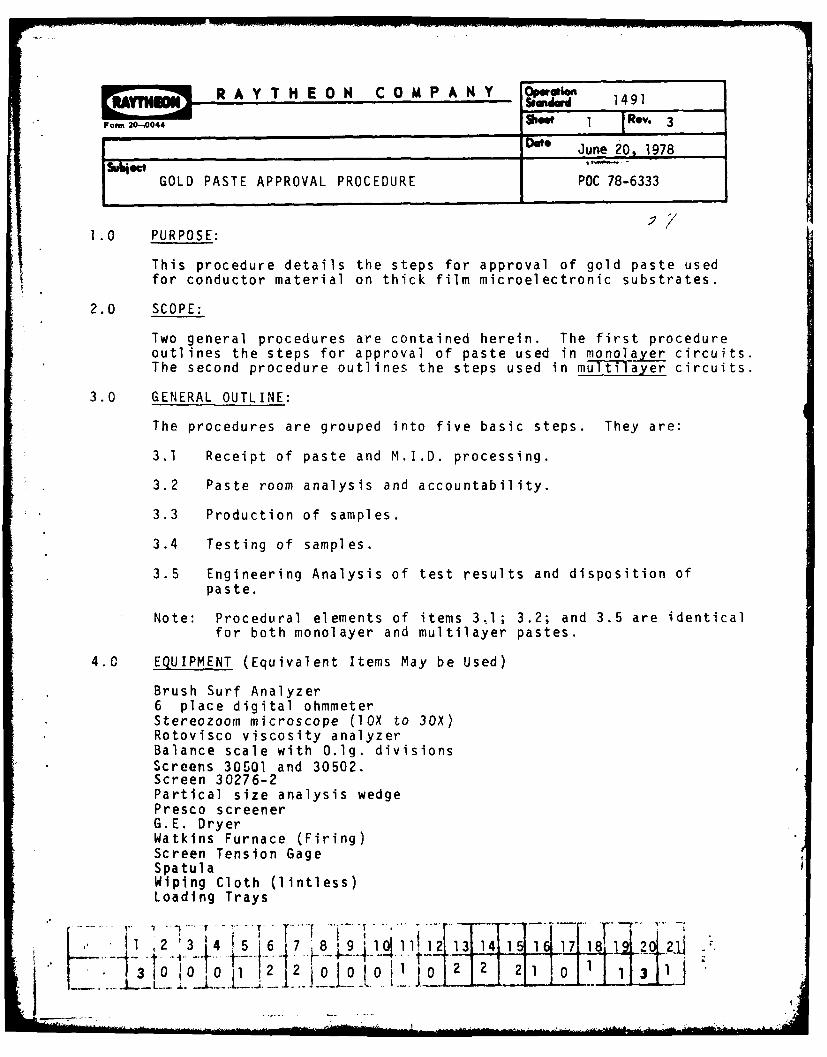
R A Y T H E 0 N C 0 M P A N Y 0eretle 1S~awd 1491
Foimn 0-"0044 Shoo 1 _ Rev. 3June 20, 1978
GOLD PASTE APPROVAL PROCEDURE POC 78-6333
1.0 PURPOSE:
This procedure details the steps for approval of gold paste usedfor conductor material on thick film microelectronic substrates.
2.0 SCOPE:
Two general procedures are contained herein. The first procedureoutlines the steps for approval of paste used in monolayer circuits.The second procedure outlines the steps used in multilayer circuits.
3.0 GENERAL OUTLINE:
The procedures are grouped into five basic steps. They are:
3.1 Receipt of paste and M.I.D. processing.
3.2 Paste room analysis and accountability.
3.3 Production of samples.
3.4 Testing of samples.
3.5 Engineering Analysis of test results and disposition ofpaste.
Note: Procedural elements of items 3,1; 3.2; and 3.5 are identical
for both monolayer and multilayer pastes.
4.0 EQUIPMENT (Equivalent Items May be Used)
Brush Surf Analyzer6 place digital ohmmeterStereozoom microscope (IOX to 30X)Rotovisco viscosity analyzerBalance scale with 0.1g. divisionsScreens 30501 and 30502.Screen 30276-2Partical size analysis wedgePresco screenerG.E. DryerWatkins Furnace (Firing)Screen Tension GageSpatulaWiping Cloth (lintless)Loading Trays
1 ...... -35_ 7 ' 8 9 1 11112 13 14... . 17.. 18' 1 2.... .+,4-4- 3l
10______ __11_2__0. JO 0__ _ _ _ _
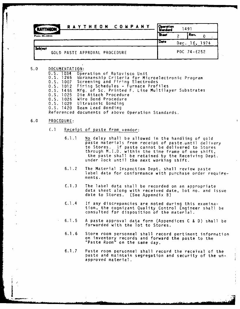
R A Y T H E O N C 0 MP A N Y Oa 1supdm 149 1
Form 20-0044 Shw 2 Rev. 0Date Dec. 16, 1974
GOLD PASTE APPROVAL PROCEDURE POC 74-(252
5.0 DOCUMENTATION:O.S. 1034 Operation of Rotovisco UnitO.S. 1265 Workmanship Criteria for Microelectronic ProgramO.S. 1007 Screening and Firing ElectrodesO.S. 1012 Firing Schedules - Furnace ProfilesO.S. 1455 Mfg. of Sc. Printed F. Line Multilayer SubstratesO.S. 1025 Die Attach ProcedureO.S. 1026 Wire Bond ProcedureO.S. 1029 Ultrasonic BondingO.S. 1420 Beam Lead BondingReferenced documents of above Operation Standards.
6.0 PROCEDURE:
[.1 Receipt of paste from vendor:
6.1.1 No delay shall be allowed in the handling of goldpaste materials from receipt of paste.until deliveryto Stores. if paste cannot be delivered to Storesthrough M.I.D. within the time frame of one shift,the paste shall be retained by the Receiving Dept.under lock until the next working shift.
6.1.2 The Material Inspection Dept. shall review pastelabel data for conformance with purchase order require-ments.
C.1.3 The label data shall be recorded on an appropriatedata sheet along with received date, lot no. and issuedate to Stores. (See Appendix B)
C.1.4 If any discrepancies are noted during this examina-tion, the cognizant Quality Control Engineer shall beconsulted for disposition of the material.
6.1.5 A paste approval data form (Appendices C & D) shall beforwarded with the lot to Stores.
6.1.6 Store room personnel shall record pertinent informationon inventory records and forward the paste to the"Paste Room" on the same day.
6.1.7 Paste room personnel shall record the receival of thepaste and maintain segregation and security of the un-approved material.
i.
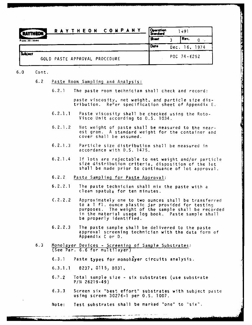
RAYTHEON COMPANY Op 149
Fonm 20-0044 Shoo 3 1 Rev. 0Dte Dec. 16, 1974
sbect GOLD PASTE APPROVAL PROCEDURE POC 74-6252
6.0 Cont.
6.2 Paste Room Sampling and Analysis:
6.2.1 The paste room technician shall check and record:
paste viscosity, net weight, and particle size dis-tribution. Refer specification sheet of Appendix E.
6.2.1.1 Paste viscosity shall be checked using the Roto-Visco Unit according to O.S. 1034.
6.2.1.2 Net weight of paste shall be measured to the near-est gram. A standard weight for the container andcover shall be assumed.
6.2.1.3 Particle size distribution shall be measured inaccordance with O.S. 1475.
6.2.1.4 If lots are rejectable to net weight and/or particlesize distribution criteria, disposition of the lotshall be made prior to continuance of lot approval.
6.2.2 Paste Sampling for Paste Approval:
6.2.2.1 The paste technician shall mix the paste with aclean spatula for ten minutes.
(.2.2.2 Approximately one to two ounces shall be transferredto a I fl. ounce plastic jar provided for testingpurposes. The weight of the sample shall be recordedin the material usage log book. Paste sample shallbe properly identified.
6.2.2.3 The paste sample shall be delivered to the pasteapproval screening technician with the data form ofAppendix C or D.
6.3 Monolayer Devices - Screening of Sample Substrates:
(See Par. 6.6 for multilayer)
E.3.1 Paste types for monolayer circuits analysis.
6.3.1.1 8237, 81153 8831,
6.?.2 Total sample size - six substrates (use substrateP/N 26219-49)
6.3.3 Screen six "best effort" substrates with subject pasteusing screen 30276-1 per O.S. 1007.
Note: Test substrates shall be marked "one" to "six".
RAYTHEON COMPANY 0UPw 1491
,omi 20-0044 Sh.o 4 R*v. 0..I e Date Dec. 1E, 1974
GOLD PASTE APPROVAL PROCEDURE POC 74-(252
6.0 Cont.
6.3.4 Rescreen substrates one and two per O.S. 1007.
6.3.5 Fire all six substrates two times per O.S. 1012.
6.4 Testing/Inspection of Sample Substrates (Monolayer)
6.4.1 Check substrates one and two for bubbling under 30X & (OXmagnification and record data on data sheet of Ap-pendix C.
6.4.2 Submit substrates 3 through 6 to visual examinationunder lOX to 30X magnification per the criteria ofO.S. 1265, Section 300 and the applicable items ofSection 100. Record information on data sheet ofAppendix C.
6.4.3 Submit the four substrates to the cognizant QualityControl Engineer for resolution evaluation. Resultsshall be recorded on the data sheet of Appendix C.
6.4.4 Check resistivity run of all substrates per the in-struction of Appendix A. Record results on the datasheets on Appendices A-l and C.
6.4.5 Submit substrates 3 through E to the Chip and ,.fireDept. for attachment testing.
6.4.5.1 Submit 1 piece for beam lead device attachment perO.S. 1420. Five devices shall be attached to thesample substrate. The sample attachments shall besubjected to inspection per the criteria of par. 8of O.S. 1265.
6.4.5.2 Submit 1 piece for thermo-compression wire bondingper O.S. 1026. Fifty stitch bonds shall be madeusing production gold wire. The bonds shall be eval-uated to the applicable criteria of O.S. 1265 par. 3.All fifty wires shall be pulled for evaluation to thecriteria of par. 3.1E of O.S. 1265.
6.4.5.3 Submit 1 piece for ultrasonic wire bonding per O.S.1029. Same test as in 6.4.5.2.
RAYTHEON COMPANY o,.,.atn1. ... wd 1491
Show 5 Rev. 1Dote March 5, 1975fg GOLD PASTE APPROVAL PROCEDURE POC 75-E050
6.0 Cont.
6.4.5.4 Submit 1 piece for die attachment. Ten (10,dice shall be attached using eutectic bondinrjtechnique per O.S. 1025. The bonded dice shallbe evalu3ted to the applicable criteria ofO.S. 1265, Sheet 8.
6.4.5.5 All inspection results of paragraph 6.3.9 shallbe recorded on the data sheet of Appendic C.All samples shall be forwarded with the dat,sheet in such a manner to prevent handling damnge.
E.5 Engineering Review and Disposition:
6.5.1 The cognizant Quality Control and Screening Engineersshall review all approval data and provide dispositionon the approval farm of Appendix E. Any use restrictionsshall be noted on the form.
6.5.2 Copies of the approval and data forms shall be forwarde,:to M.I.D.; the Paste Room technician, and the cognizantScreening Room En]ineer. If restrictions are noted onthe approval form an extra copy shall be forwarded toM.I.D. A copy of the approval form only shall be for-warded to Production Control.
6.5.3 Upon receipt of an approved form, the M.I.D. inspectorshall label the subject paste jar with either an acceptor reject notation, If a restriction is noted on theapproval form, a notation on the jar shall be placedwith the words "Restricted - Use". A copy of the approvalform shall also be provided by M.I.D. and placed with thesubject jar, if the jar has a use restriction.
6.5.4 Rejected jars shall be placed in a special uReject Drawer"until appropriate disposition of the rejected jar is made.
6.6 Screening and Testing of Sample Substrates for Multilayer Devices:Refer to Sheet 20 for Applicable Paste Types.
6.6.1 Total sample size - 12 pieces.
6.C.2 Apply numbers to each test substrate - "one' to "twelve"
6,6.3 Screen conductor material under test on all test substratesper O.S. 1007 using screen 30502.
6,6.4 Fire all twelve substrates per O.S. 1012.
*Refer Appendix G for applicable dielectric material.
RAYT H E ON COMPANY ration 1491
Form 20-0044 she 6 Re. 2
'k April 25, 1975subigct
GOLD PASTE APPROVAL PROCEDURE POC 75-6081
6.0 Cont.
6.6.5 Screen dielectric on half the substrate using screenno. 30276-2. Dielectric material will be determinedby Engineering prior to start of test. Refer O.S. 1455.(12 pieces)
6.6.6 Fire dielectric per O.S. 1455. (12 pieces)
6.6.7 Screen conductor material under test on all test sub-strates per O.S. 1007 using screen no. 30501. This goldscreening is screened on the dielectric surface.
6.6.8 Fire all substrates per O.S. 1012,
6.6.9 Substrates one, two, ten and eleven, rescreen subjectgold paste per O.S. 1007 using screen 30501.
E.6.10 Fire substrates one and two per 0,S. 1012 and O.S. 1007.
6.6.11 Substrates 5 through 8, refire an additional two timesper O.S. 1012.
6.6.12 Substrates 9 through 12, refire an additional 13 timesper O.S. 1012.
6.6.13 Visually inspect substrates one and two for bubblinqunder 30X magnification and record data on data sheetof Appendix D, Repeat examination under 60X.
6.6.14 Visually inspect substrates one and two to the criteriaof O.S. 1265, 300 series.
6.6.15 Screen substrates one, two, three, and four with die-lectric using screen 30501 per O.S. 1455.
6.6.16 Fire substrates one through four per O.S. 1455.
6.6.17 Rescreen substrates one through four with dielectriusing screen 30276-2 per O.S. 1455*.
6.6.18 Fire substrates cne through four per O.S. 1455.
6.6.19 Submit substrates one through four to Quality ControlInspection for evaluation of bubbling effects of die-lectric on gold. Results are to be recorded on thedata sheet of AoFendix D. Check under 30X and fOX m'.y-nification. Testing of substrates 1, 2, 3, and 4 endswith this examination. Seal in envelopes and retainwith test lot.
*Refer Appendix G for applicable dielectric material.
rR-VT ng R AY TH EO0N COM P AN Y Oprloku -°rd 1491
Form 20-0044 US Re. 2Doe April 25, 1975
Sj GOLD PASTE APPROVAL PROCEDURE POC 75-6081
6.0 Cont.
6.6.20 Check substrates 7, 8, 11, 12 for gold resistivityaccording to the instruction of Appendix A.Record data on Appendix A-1 and D.
6.6.21 Submit substrates seven through twelve to QualityControl Inspection for evaluation of resolution.Results are to be recorded on the data sheet of Ap-pendix D.
6.6.22 Check substrates five through twelve visually to thecriteria of O.S. 1265, 300 series. Also check sub-strates 9 - 12 for gold/glass segregation under 200-300X magnification.
6.6.23 Check substrates 5 through 12 for quality of the follow-ing attachments. See schedule below. Results are tobe recorded on the data sheet of Appendix D. Follow theinstruction of paragraph 6.4.5.
6.6.23.1 Beam lead attach-substrates 5 and 9.
6.6.23.2 Thermocompression wire bond-substrates 6 and 10.
6.6.23.3 Ultrasonic wire bond-substrates 7 and 11.
6.6.23.4 Eutectic die attachment-substrates 8 and 12.
6.7 Engineering Review and Disposition of Multilayer Gold DasteTest Results. Follow instruction of paragraph 6.5.
Note: A combination of acceptable results for substrates 5 through8 and rejectable results for substrates 9 through 12 may resultsin the downgrading of multilayer gold paste to monolayer applici-tion.
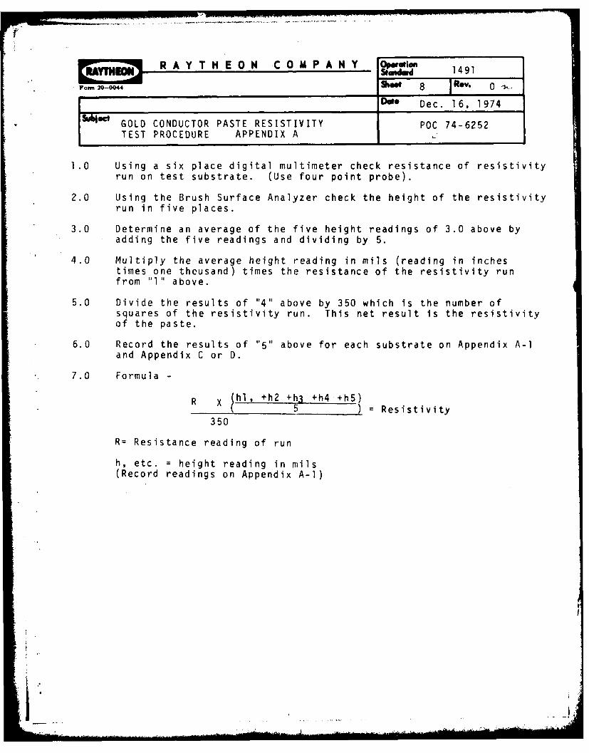
R A Y T H E 0 N C 0 M P A N Y OrInSeu~dwd 1491
Fon,, 20-0044 3609 8 - Rev. o0~.DUi Dec. 16, 1974
GOLD CONDUCTOR PASTE RESISTIVITY POC 74-6252TEST PROCEDURE APPENDIX A
1.0 Using a six place digital multimeter check resistance of resistivityrun on test substrate. (Use four point probe).
2.0 Using the Brush Surface Analyzer check the height of the resistivityrun in five places.
3.0 Determine an average of the five height readings of 3.0 above byadding the five readings and dividing by 5.
4.0 Multiply the average height reading in mils (reading in inchestimes one thousand) times the resistance of the resistivity runfrom "1" above.
5.0 Divide the results of "4" above by 350 which is the number ofsquares of the resistivity run. This net result is the resistivityof the paste.
6.0 Record the results of "5" above for each substrate on Appendix A-iand Appendix C or D.
7.0 Formula -
R x (hI, +h2 +h3 +h4 +h5)( 5 ) Resistivity
350
R= Resistance reading of run
h, etc. = height reading in mils(Record readings on Appendix A-i)
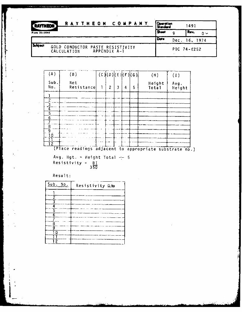
R A Y T H E 0 N C 0 M P A N Y ion 14S~u~derd 1491
Fon 20-0044 Uhit 9 T Rev.
Date Dec. 16, 1974
"i4't GOLD CONDUCTOR PASTE RESISTIVITY POC 74-f252CALCULATION APPENDIX A-P
(A) (B) (C)(D)(E)(F)(G) (H) MI)
Sub. Net Height Avg.No. Resistance 1 2 3 4 5 Total Height
2
' , . . . ... .. . .- I
...... . - - -:_ _ _ _ __ _ _ _ _
"5 .. . . . . .. ... . .. ... . . . ..."-------_- -
7 ...... ..... _- - _
8- - -- .. . . . . . .. . . . ... - .... ... .. " -" _ _ - ,_
(Place readings adjacent to appropriate substrate no.)
Avg. Hgt. = Height Total -- 5Resistivity = BI
350
Result:
Sub. No. Resistivity 0/0
1234
56
8
0
12
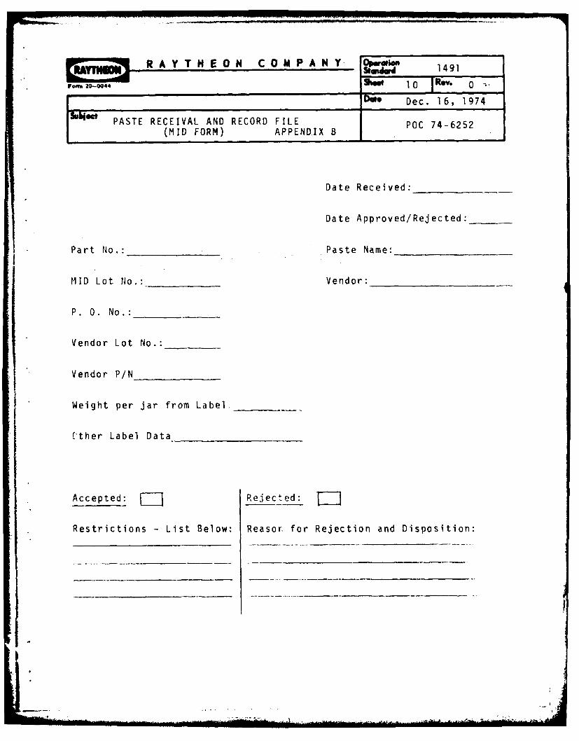
orm 20-0044 94Wi 10 IRO. 0
Do Dec. 16, 1974
PSERECEIVAL AND RECORD FILE O 7465PASTE (MID FORM) APPEND.IX BPC7-25
Date Received:_________
Date Approved/Rejected:____
Part No.: _________Paste Name:___________
MID Lot No.: _______Vendor: ___________
P . 0 . No .: ______
Vendor Lot No.:_____
Vendor P/N________
Weight per jar from Label. ____
('ther Label Data __________-
Accepted: [~jRejected: lzRestrictions -List Below: Reason. for Rejection and Disposition:
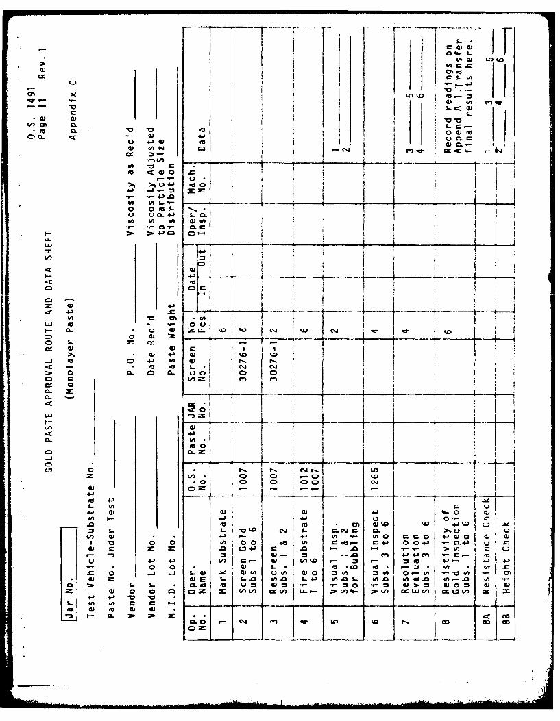
-. 04- 5-~----.jA- 4) 1- kI AA m k
0-0CL~
.q- AA4N
a,~ ,
a, 0n to~
u ~ U 0-4 -C
V) 4)9 Lo 0)I
o ciaL L-r_=Po 004) 9= =U, U U t,r 0L0.
a) 4
cm --10J0
C) 4)r.K
to to zo. t>. ~ , u 0
C) a, m)Io t
CCL
a-4 2
to 0
Ch a-
a.. U. LO
V; - ' 0 C) r-CD0 C) 0 C)oCl
(a 4)
41 4) 4J 0'to L L1 1t C*J I 0C E
Ln w, .P (A - r- U, Wn C O a0 a, el"0~ 0 CA 00 oe U) Can r- E4J 0 04) *0. 4J u
a, CV r_ .0 C5 4.) r .0 I- .0 > CA*' r_ Lp.-~~~ V- u-.
0 -V r)-e) iE- 'a
u 4)P 4 Ln9 E- 4, L~ %0 = =' +A.- " ) 4*0 0a I Vk L va*pa* .- n * U
4) a, 0 1-I. L. 0 o .0 S-41 4A .0L (A .0 W)'to0m UCA -. 0 CA0 1 %- S. CX to M. ' U = .~ = - *u- = 0 =o a, >a,) c
w 0 0 L ~ Z C4
) V) LL.- fI- Ln W LLt,') ccCDI0 Ul
LL U, U, 40 LO r, O___ 00_ co_ _ _
'a~( 2Ma a
o II
0) W
S- a'
I!Ij
,w 0. ,
"!I I
Cc
s.- . I
CD I CD CDl
O-- r ' -. - __ _ _ _ _ _ _ __ _'U I
o CD
- - .- c a - t -_ IA
L1 _ _ _ _0 _ _ . +
0 m .0 CO CO LA U .
*C 0 = w 0& (V w m C C.Jo 0 - - i- w- - - - - S
0. LO M
o00 0
-- U 0 E 'a 'a 'a .- A-$-G E' 50E . L .' * z r- 0) La- G G J ,-. " € r.
.-
• f0
C4
- 0
m ex u 4J 4-)OO 96 -cc V to
to CC 0 _ _- --CA
>-, > * 4-4-) 4J') (D
AU.- to~. 0
0 0J.-) - -
u~ L) 4J ) .
U~.. >. In d)U
4-)
ol 4-) m
*~ 0 4-)
>1 0 1 - 0 a) .Inl C4 ci CM r l
o 2= 0 : (L) = 0 CJ Cj C. % 'J (J CJ ~ C
4) -4 -
S 4.' 4-) (A) 0 '.
o~t to 0- 0 Da)C) tm -L 00
w0 X S. 00 r I C)0- uA 0 0M 0r
(l. V) C
I- S-
o 4-3
'.- r- U-) It) C. (\J CD C C C)N
a 0 0D D .c .r 0: 00 0= 00 C C C C>
to 4-'
4J~ GI 40 C. I--
U I.
Ifl. C) * C .
IL 00 0 S--4-
a) v4 4-3 4J 4J W =S CJ LO*w 03 0- Sn- S- u u u W Ln
al 0 0 4-4' a 4) 4) =- = ) L-\ "a
4J = 4 "0 E -W La) 8)4- w 38 4) 41LWO 4 a U )(
OA 14- V) c m to $- L. .0 S- La) La)( L a LC (A IA L. to U..0Go 4jot 0 CD tu Ci O= o- .-' *.- 0 0 *0 010 -
X: VI .~ Ld LA- LAol 3 L-i VA) U U ) C_ c L-. ULA )
C m r Ln W r- 00 0C) '3 () t O N
IA
Im -0 -
aJ ..- C-J
O~CL
u D- 0.4
CL 41 ocx c
M
'u,
V) C)
C,
F-I
w >- 0
a, -. 1-.
0C) Cj
V)'
LLiS-
4-) m C)c')CD V) o0CD
* ~ r'4N UC) L) LC) IL LA-I C) ,-O' LA) Lo LA LA)
o l Co 04- -
C C'
- 4J 4- 0-
=, tm a) w, m + -,--inrcCJ .0d I q* .- I* >,o, U u
.- 0 4A a C 4)- 4-a 4) a, d C
.0 -' 0 0 . >0 > LA Lc0m ')' 4m .. r- 00) U 4J + .0 .- N a I
S. aU u =1 (L (AL U -~ LL 4-~~c ) 4J 4-3
4J 0 a III a. 0A = 4A C4-) CA 6) 041 0 () Q. z ' 0 00 C) L.0 S.L.0 IA .0 L. L J3f-1 0 .0 S. ~L. CA-. 0A) -
(% en ~ %t 0W) *' ~ *.- C*.o al~ m)
ChwrL
V) m C
to -o
.41
LILUJ
LV)
S-
In 01
I- 0 1
S. 41
C)C
0 0O~ CD ('J toi C\J
00 <sJ LL - - ~ C-* 7-J -
I LL.0 I
W E ra c 0 ON 0E u
00 0~ a0 0 -
to 04 C' e-. V ) ok C)C
040VC ~ ~ 4 0 l
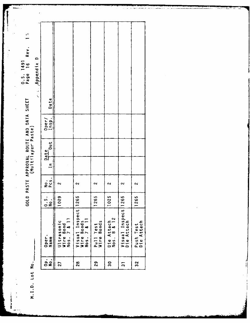
@3
0b 0
*LJ4-
.43 do
mi 4-)
Ci)
LOLOL .) f
co @3U
4) W
00 0)I __) __ 4 _4
0(O3 M' C% D 04 '.
0 - -- -- -- - 4
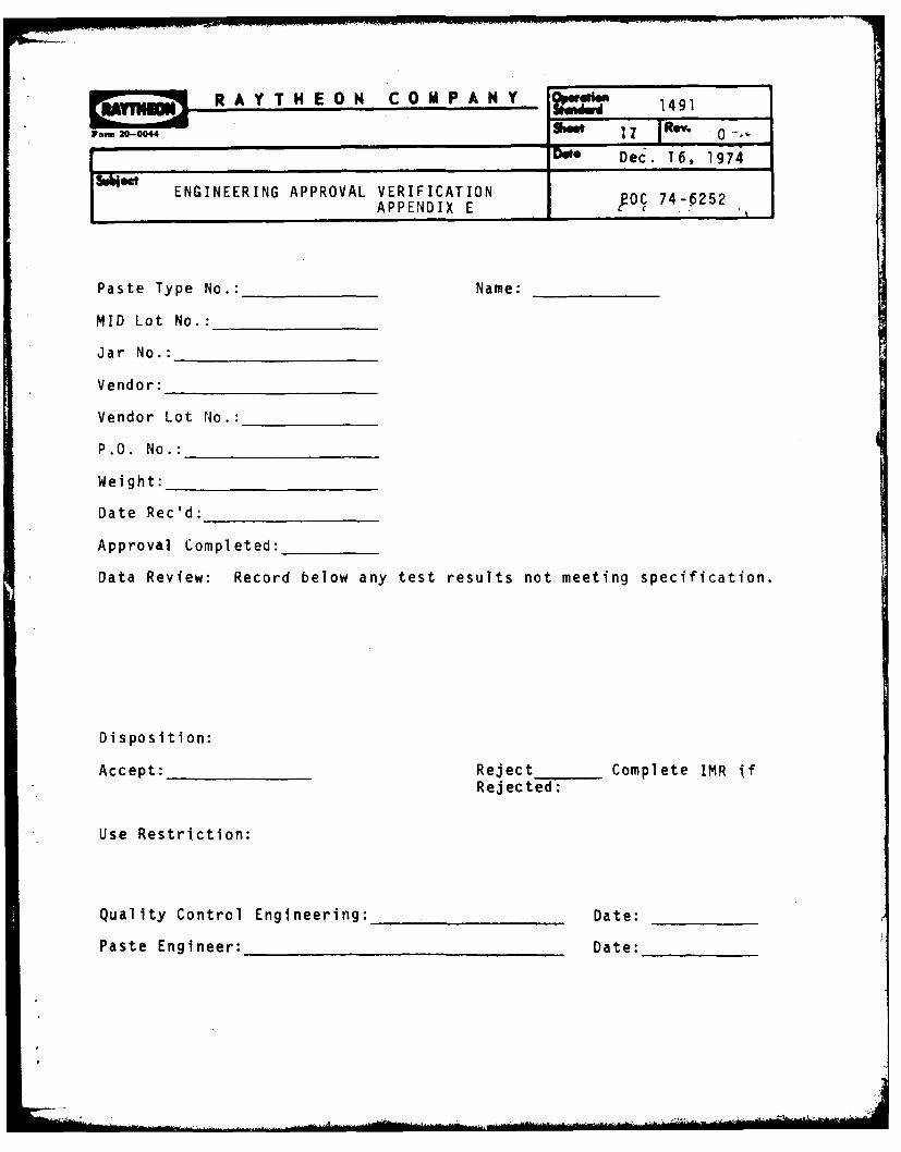
Fomi 20-0044 tv 0
ENGINEERING APPROVAL VERIFICATION 7-65
Paste Type No.: ________Name:_______
MID Lot No.: _________
Jar No.:__ _ _ _ _ _ _ _ _ _ _
Vendor: _____________
Vendor Lot No.:________
P.O. No.:__ _ _ _ _ _ _ _ _ _
Wei ght: _____________
Date Rec'd:_____ _____
Approval Completed: _____
Data Review: Record below any test results not meeting specification.
Disposition:
Accept: _________Reject____ Complete IMR tfRejected:
Use Restriction:
Quality Control Engineering: ___________ Date: ______
Paste Engineer: ___________________ Date:_______
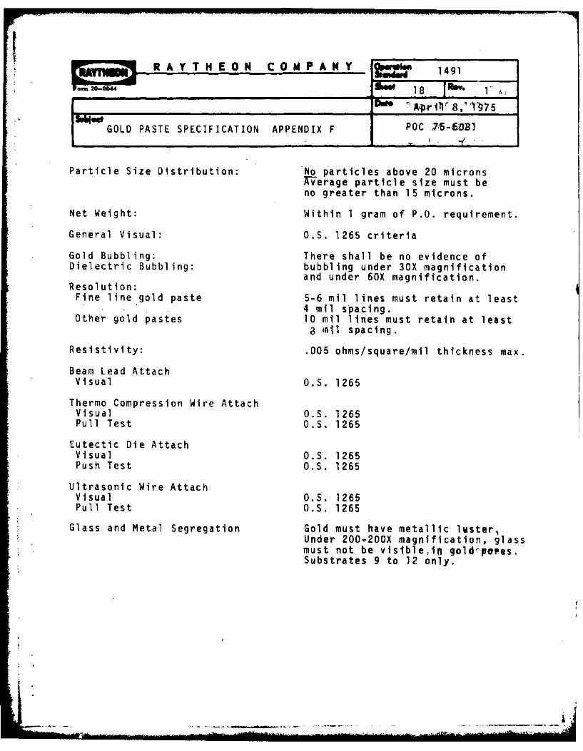
R A Y T H E 0 N C 0 M P A H Y
GOLD PASTE SPECIFICATION APPENDIX F P0C 1715-6.OBI
Particle Size Distribution: No .particles above 20 micronsTverage particle size must beno greater than 15 microns.
Net Weight: Within 1 gram of P.O. requirement.
General Visual: O.S. 1265 criteria
Gold Bubbling: There shall be no evidence ofDielectric Bubbling: bubbling under 30X magnification
and under 60X magnification.Resolution:Fine line gold paste 5-6 mil lines must retain at least
4 mil spacing.Other gold pastes 10 mil lines must retain at least
a nil spacing.
Resistivity: .005 ohms/square/mil thickness max.
Beam Lead AttachVisual O.S. 1265
Thermo Compression Wire AttachVisual O.S. 1265Pull Test O.S. 1265
Eutectic Die AttachVisual O.S. 1265Push Test O.S. 1265
Ultrasonic Wire AttachVisual O.S. 1265Pull Test O.S. 1265
Glass and Metal Segregation Gold must have metallic luster,Under 200-200X magnification, glassmust not be vislble,in gold-popes.Substrates 9 to 12 only.
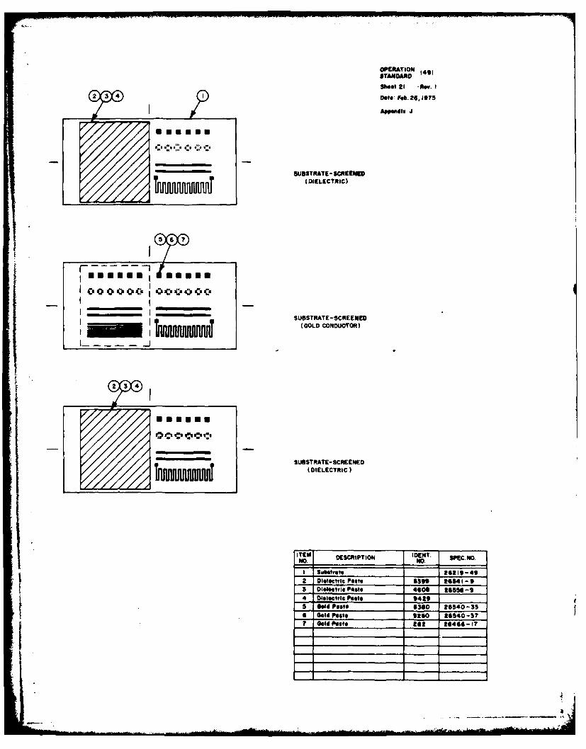
OPERATION 1491STANDARDShoot 2I nRow. I
Data: F.e 26.197
op Appendix J
SUBSTRATE- SCREENIEDTni l~lh~llJU~I1 ~(DIELECTRIC)
SUSSTRATE -SCREENED(GOLD CONDUCTOR)
SUbSTRATE- SCREENED
WNW(DIELECTRIC)
ITEM DESCRIPTION WDENT. K.ONO.C NO.
I Substrate ____26219-49
2 Dieetric Paste 655" 2541 -93 Dielectric Paste 4606 26556-94 Dielectric Peste 94t9 ______
5 sold Pestil 6390 26540-35e cld Paste 911:0 261406-I7
T sold Pests t2at 26140 -3?
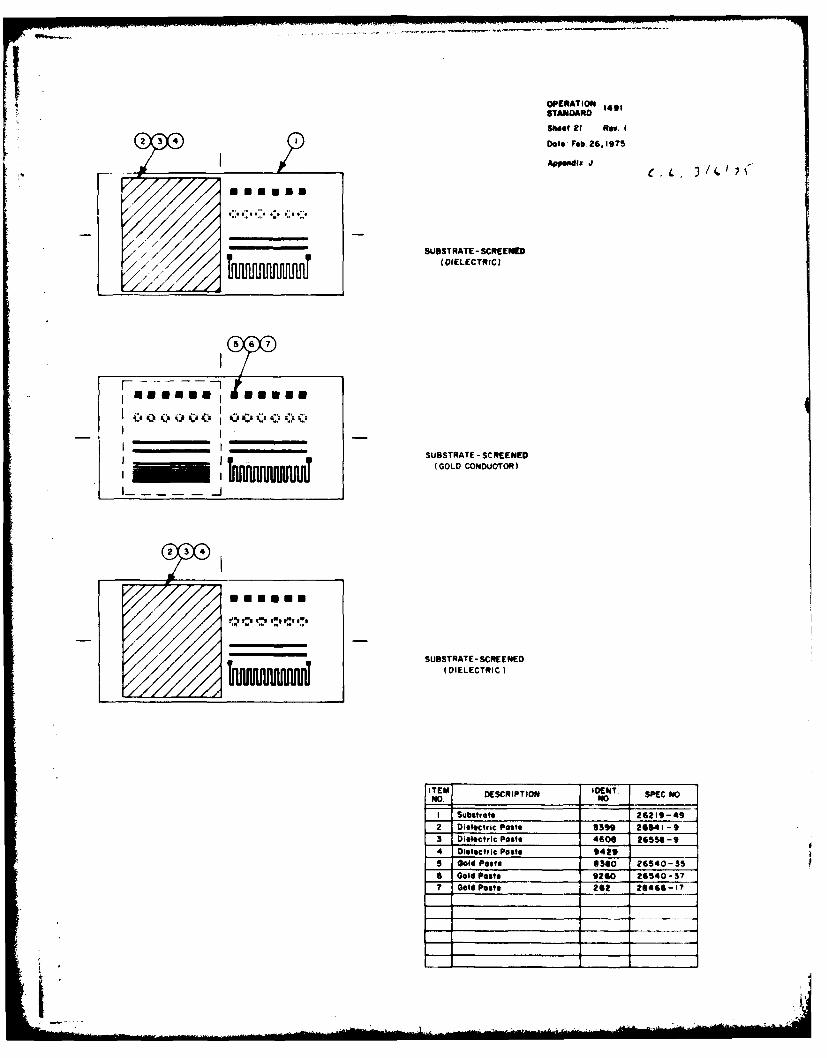
OPERATION4 1491STANDARD
Shoot 21 Rev. I
Date Feb. 26.1975
Appendix J
SUBSTRATE- SCREEME(DIELECTRIC)
SUBSTRATE -SCREENEDTnnflnnnw (GOLD CONDUCTOR)
SUBSTRATE- SCREENEDT'duull(DIELECTRIC)
tITEM DESCRIPTION iDENT SPEC No
I Substrate 26219-492 Dielectric Poste 6399 26541-93 Dielectric Paste 4606 26550-94 Dielectric Past* 9429 _____
5 sold Paste 6360 26540-356 Gold Posts 9260 26540-37
S.. . ad 1493
Nnv.mh r 1A, 1977
POC 77-6517[.. ...CLEANING OF ARCO MODULES
1.0 PURPOSE:
To remove flux and surface contamination.
2.0 MATERIALS:
2.1 Freon TP-35 duPont
2.2 Isopropyl Alcohol-electronic grade or MOS grade
2.3 Glass Beakers
2.4 Hot Plate
3.0 PROCEDRUE:
*3.1 Fill appropriate size beaker with clean Freon TP-35.
3.2 Completely immerse modules in TP-35 and hold until readyfor step 3.3. Allow two minutes from removal from solderingheat columns and immersion.
3.3 Remove modules from TP-35. Discard TP-35. Brush with TP-35to remove any visible contamination.
3.4 Reimmerse modules in a clean beaker filled with clean freonTP-35 and boil for a minimum of five minutes.
3.5 Remove from heat and let stand five minutes at room temperature.
(Note: this step is necessary to avoid thermal shock).
3.6 Remove modules from TP-35 and allow excess solvent to stand off.
3.7 Immerse modules in clean isopropynol and allow to standten minutes at room temperature.
3.8 Remove from isopropynol and allow to dry in air.
*Note: By clean it is ment as received from the vendor and approved
by M.I.D.
~~R A Y T H E 0 H C 0 M P A N Y 1494 .. i i
.. ..- Feb. 19, 1979
S REFLOW SOLDERING (USING IRON TO REFLOW)
1.0 PURPOSE:
To attach discrete components such as diodes, transistors, capacitors,
jumpers and leads to pre-timmed substrate.
2.0 SAFETY:
Use normal precautions around hot soldering tools.
3.0 APPLICABLE DOCUMENTS:
Assembly drawing for each module.
4.0 EQUIPMENT, TOOLS, GAUGES:
4.1 Tweezer #3 or equivalent (non-metalic for leadless devices).
4.2 Cutters
4.3 Flux dispenser EPE Corp. FD-2-1 (.010 dia. needle) or equiv.
4.4 Soldering iron as specified in Table I.
4.5 Heat column (135+160C) with vacuum hold down.
4.6 Variac for heat column.
4.7 Microscope - B & L 7X to 30X Stereozoom or equivalent.
4.8 Toothpicks, wooden.
5.0 PROCESS REQUIREMENTS:
5.1 Materials:
5.1.1 Solder - Type WRMAP2 (Alpha Reliacore 11) QQS-571E orWS of Fed. Spec. QQS571E.
5.1.1.1 60% Sn for parts without silver-bearingterminations.
5.1.1.2 62% Sn, 36% Pb, 2% Ag for parts with silver-bearing terminations.
1 2 '3 II TTTT'T42
. . . .. _ . 4 - ..... _. .
~~R A Y T H E 0 N C 0 M P A N Y 191494
. .... __ Feb. 19, 1979
REFLOW SOLDERING (USING IRON TO REFLOW) POC 79-6109
5.1 Cont.
5.1.1.3 96% sn, 4% Ag when specified on drawing.
5.1.2 Flux - Alpha #611
5.1.3 Flux cleaner - Freon TP35 and Isopropanol.
5.2 PROCEDURE:
5.2.1 Cut and bend leads of components to fit the conductor padsaccroding to applicable assembly drawing. Leads bends shallhave radius of not less tha 1.5 times diameter of the wire.
5.2.2 Place components ready to assemble in bins or cups next tothe substrate heat column.
5.2.3 Place substrate on heat column with vacuum hold-down activated.Manipulate heat column so area to be bonded is microscopefield.
5.2.4 Using tweezers, pick up components, place in position onsubstrate. Flux from dispenser as necessary. While solderinghold cap in position with toothpick or nonmetalic tweezers.
5.2.5 Flow solder onto leads by touching with hot iron. Additionalsolder may be added where required to achieve a good jointper product requirements.
5.2.6 When assembly process is interrupted for more than two minutes,remove substrate from heat column.
5.2.7 Heat column temperature to be monitored daily be QC personnel,- 135 + 16'C. Settings for soldering iron to be per Table I.After assembly is completed remove from hot plate and cleansubstrate with Freon TP35 and a soft brush to remove alltraces of flux. Do not dip in Freon or other solvent immediatelyafter soldering unless solvent is heated. Allow substrate tocool to room temperature first.
6.0 QUALITY:
6.1 Workmanship Criteria In O.S. 1265.
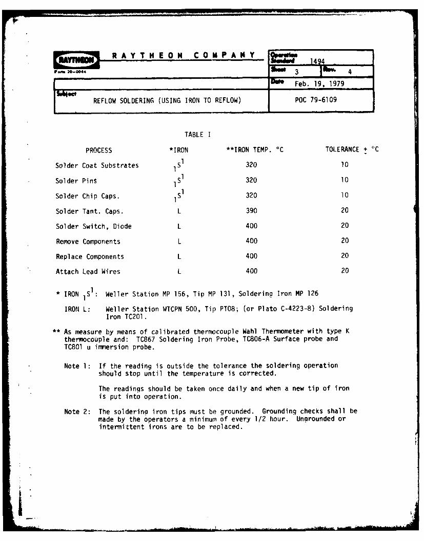
AY T HEO0N C 0
oo 20-0044 3 424
[~ jam 4rm
REFLW SODERNGD(SIN Feb. 19, 1979REFLOW SOLDERING (USING IRON TO REFLOW) POC 79-6109
TABLE I
PROCESS *IRON **IRON TEMP. °C TOLERANCE + °C
Solder Coat Substrates IS1 320 10
Solder Pins iSl 320 10
Solder Chip Caps. iS1 320 10
Solder Tant. Caps. L 390 20
Solder Switch, Diode L 400 20
Remove Components L 400 20
Replace Components L 400 20
Attach Lead Wires L 400 20
* IRON Sl: Weller Station MP 156, Tip MP 131, Solderina Iron MP 126
IRON L: Weller Station WTCPN 500, Tip PT08; (or Plato C-4223-8) SolderingIron TC201.
** As measure by means of calibrated thermocouple Wahl Thermometer with type Kthermocouple and: TC867 Soldering Iron Probe, TC806-A Surface probe andTC801 u immersion probe.
Note 1: If the reading is outside the tolerance the soldering operationshould stop until the temperature is corrected.
The readings should be taken once daily and when a new tip of ironis put into operation.
Note 2: The solderina iron tips must be grounded. Grounding checks shall bemade by the operators a minimum of every 1/2 hour. Ungrounded orintermittent irons are to be replaced.
I.
R A Y T HE 0 N C 0 M P A N Y 19RAYTHEON COM AN W=m 1498
Fon, 20-0044 Shet 1 Rev. 0 ,
_ _ _ _ _ _ _ _Doe Feb. 12. 1975
GOLD-PLATINUM PASTE APPROVAL PROCEDURE POC 75-6022
e- -
1.0 PURPOSE:
This procedure details the steps for approval of Gold-Platinum pasteused for conductor material on thick film microelectronic substrates.
2.0 SCOPE:
The procedure provides instruction for all phases of the approvalsystem from receipt of paste to Engineering Review of inspectiondata. The approval samples are inspected/tested for visual criteria,adhesion and resistivity.
3.0 EQUIPMENT: (Equivalent Items may be used)
3.1 Dip solder process station
3.2 Presco Screener
3.3 Electrode Screen (Test Pattern) P/N 30409
3.4 Watkins Johnson Furnace.
3.5 Marking Pencil (Aluminum)
3.6 Soldering Iron (17W)
3.7 Soldering Iron tip 1/32"
3.8 Digital Ohmmeter (6 place)
3.9 Wire: 26 AWG Tinned Copper
3.10 Clevite Brush Surfanalyzer Model 150
3.11 Chatillon Push/Pull Gauge - 10 Lbs capacity.
3.12 Microscope l0-30X zoom.
3.13 Rotovisco Viscosity Analyzer
3.14 Screening Drier
3.15 Screen Tension Gage
3. 16 Spatula
I 1!2 3r 4 s 6 7 8: 9:10 .11 12 314 1 1 7 1 1
0 0000 000o,0 0o1010o
IATNO R A Y T H E O N C O M P A N I 05,W.=1498
F,,fm 20-0044 Sho 2 Rv. 0Dwe Feb. 12, 1975
GOLD-PLATINUM PASTE APPROVAL PROCEDURE POC 75-6022
3.0 EQUIPMENT: Cont.
3.17 Wiping cloth (lintless)
3.18 Loading trays
3.19 Particle Size Analysis Wedge
3.20 See also Appendix B
4.0 DOCUMENTATION:
4.1 O.S. 1007 - Screening E'ectrodes
4.2 O.S. 1011 - Screener Set-Up Procedure
4.3 0.S. 1012 - Firing Schedule Furnace Profile
4.4 0.S. 1000 - Substrate Cleanliness Test
4.5 0.S. 1034 - Operation of Rotovisco Unit
4.6 0.S. 1475 - Particle Size Dist. Analysis of Screenable Pastes
4.7 0.S. 1312 - Evaluation of a New Type of Conductor Paste.
4.8 O.S. 1452 - Honeywell Substri.te Program
4.9 MIL-STD-202D
4.10 O.S. 1265 - Workmanship Criteria for Microelectronics Programs
5.0 PROCEDURE:
5.1 Receipt of Paste From Vendor:
5.1.1 No delay shall bE allowed in the handling of gold-pTatinum paste materials from receipt of paste untildelivery to Stores. If paste cannot be delivered toStores through M.I.D. within the time frame of oneshift, the paste shall be retained by the ReceivingDept. under lock until the next working shift.
5.1.2 The Material InsFection Dept. shall review paste labeldata for conformance with purchase order requirements.
5.1.3 The label data shall be recorded on an appropriate datasheet along with received date, lot no. and issue datejto Stores, (See Appendix C).
--... ..... . .ti
R A Y T H E O N C O M P A N Y 1498
Fo3n 20-0044 tshw3 Rev. o -
DC*6 IFeb. 12, 1975
GOLD-PLATINUM PASTE APPROVAL PROCEDURE POC 75-6022
5.0 PROCEDURE: "Cont.
5.1.4 If any discrepancies are noted during this examination,the cognizant Quality Control Engineer shall be con-sulted for disposition of the material.
5.1.5 A paste approval data form (Appendices D & E) shall beforwarded with the lot to Stores.
5.1.6 Store room personnel shall record pertinent informationon inventory records and forward the paste to the"Paste Room" on the same day.
5.1.7 Paste room personnel shall record the receival of thepaste and maintan segregation and security of the un-approved materia'.
5.2 Paste Room Sampling and Analysis;
5.2.1 The paste room technician shall check and record:
Paste viscosity, net weight, and particle size dis-tribution. Refer specification sheet of Appendix G.
5.2.1.1 Paste v-scosity shall be checked using theRotovisco unit according to O.S. 1034
5.2.1.2 Net weight of paste shall be measured to thenearest gram. A standard weight for the con-tainer and cover shall be assumed.
5.2.1.3 Particle size distribution shall be measured inaccordance with O.S. 1475.
5.2.1.4 If lots are rejectable to net weight and/orparticle size distribution criteria, dispositionof the lot shall be made prior to continuance oflot approval.
5.2.2 Paste Sampling for Paste Approval:
5.2.2.1 The paste technician shall mix the paste with aclean spatula for ten minutes.
5.2.2.2 Approximately one to two ounces shall be trans-ferred to a 1 fl. ounce plastic jar providedfor testing purposes. The weight of the sampleshall be recorded in the material usage log book.Paste sample shall be properly identified.
5.2.2.3 The paste sample shall be delivered to the pasteapproval screening technician with the data formof Apperdix C.
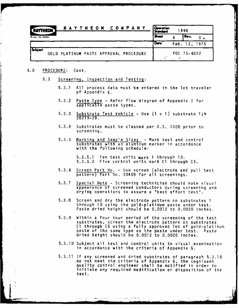
R A Y T H E ON C OM P A N Y Ow0 inrUY T "CI9 - P~w! 1498
P..m, 20-0044 Il w 7mliI 4 Rev8
Date Feb. 12, 1975
GOLD PLATINUM PASTE APPROVAL PROCEDURE POC 75-6022
5.0 PROCEDURE: Cont.
5.3 Screening, Inspection and Testing:
5.3.1 All process data must be entered in the lot travelerof Appendix E.
5.3.2 Paste T e - Refer flow diagram of Appendix I forapplicale paste types.
5.3.3 Substrate Test Vehicle - Use (1 x 1) substrate P/N26219-29.
5.3.4 Substrates must be cleaned per O.S. 1000 prior toscreening.
5.3.5 Marking and Sampie Sizes - Mark test and controlsubstrates with an al -uminum marker in accordancewith the following schedule:
5.3.5.1 Ten test units mark 1 through 10.5.3.5.2 Five cortrol units mark Cl through C5.
5.3.6 Screen Part No. - Use screen (electrode and pull testpattern) Part No, 30409 for all screenings.
5.3.7 Special Note - Screening technician should note visualappearance of screened conductors during screening anddrying operations to assure a "best effort test".
5.3.8 Screen and dry the electrode pattern on substrates 1through 10 using the gold-platinum paste under test.Paste dried height should be 0.0012 to 0.0020 inches.
5.3.9 Within a four hour period of the screening of the testsubstrates, screen the electrode pattern on substratesCl through C5 using a fully approved lot of gold-platinumpaste of the same type as the paste under test. Pastedried height should be 0.0012 to 0.0020 inches.
5.3.10 Subject all test and control units to visual examinationin accordance with the criteria of Appendix G.
5.3.11 If any screened and dried substrates of paragraph 5.3.10do not meet the criteria of Appendix G, the cognizantquality control engineer shall be notified in order toinitiate any required modification or disposition of thetest.
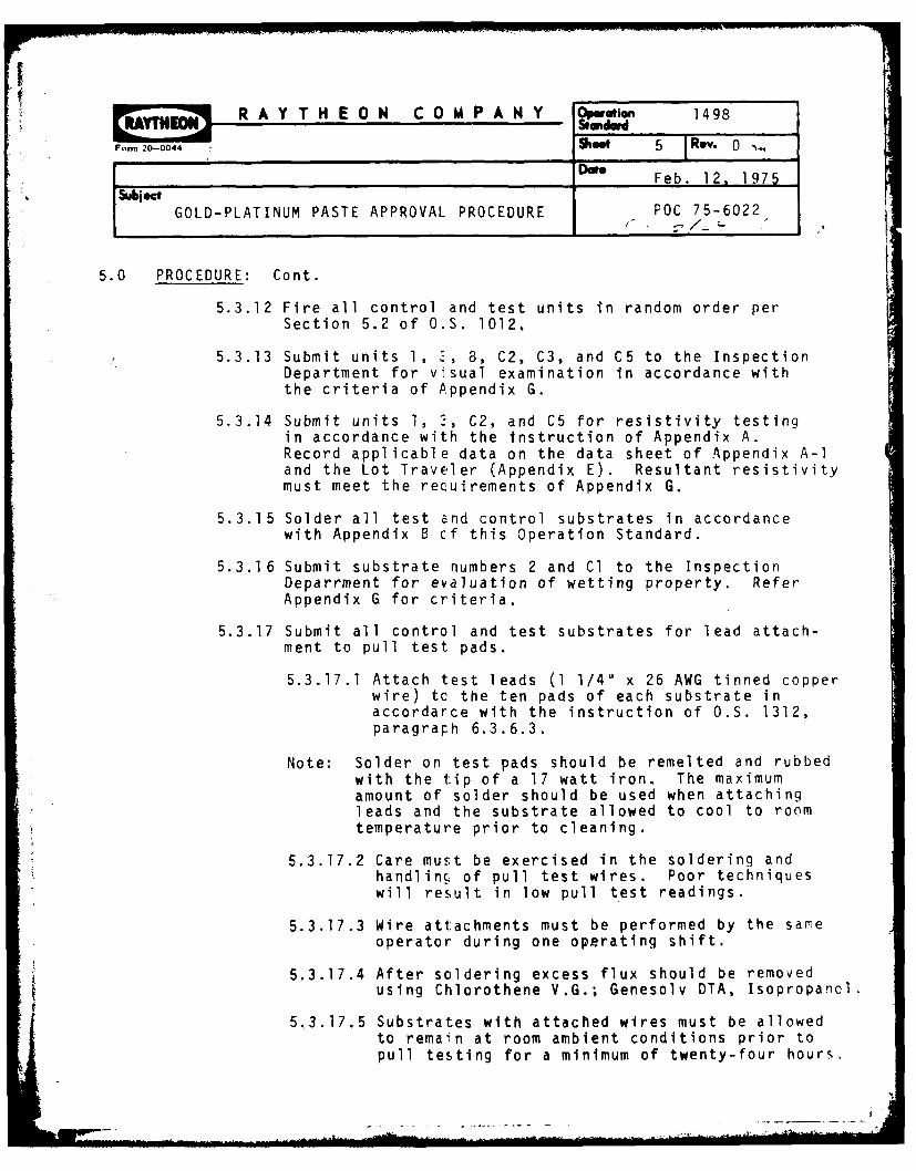
II R AY TH EO0N COM P ANHY Oeaon 1498
Form 20-0044Sho 5 Rv 0iL l~me Feb. 12, 1975
SubiectGOLD-PLATINUM PASTE APPROVAL PROCEDURE POC 75-6022,
5.0 PROCEDURE: Cont.
5.3.12 Fire all control and test units in random order perSection 5.2 of O.S. 1012,
5.3.13 Submit units 1, C, 8, C2, C3, and C5 to the InspectionDepartment for visual examination in accordance withthe criteria of Appendix G.
5.3.14 Submit units 1, _, C2, and C5 for resistivity testingin accordance with the instruction of Appendix A.Record applicable data on the data sheet of Appendix A-Iand the Lot Traveler (Appendix E). Resultant resistivitymust meet the recuirements of Appendix G.
5.3.15 Solder all test and control substrates in accordancewith Appendix B cf this Operation Standard.
5.3.16 Submit substrate numbers 2 and Cl to the InspectionDeparrment for evaluation of wetting property. ReferAppendix G for criteria.
5.3.17 Submit all control and test substrates for lead attach-ment to pull test pads.
5.3.17.1 Attach test leads (1 1/4" x 26 AWG tinned copperwire) tc the ten pads of each substrate inaccordarce with the instruction of O.S. 1312,paragraph 6.3.6.3.
Note: Solder on test pads should be remelted and rubbedwith the tip of a 17 watt iron. The maximumamount of solder should be used when attachingleads and the substrate allowed to cool to roomtemperature prior to cleaning.
5.3.17.2 Care must be exercised in the soldering andhandling of pull test wires. Poor techniqueswill result in low pull test readings.
5.3.17.3 Wire attachments must be performed by the sameoperator during one operating shift.
5.3.17.4 After soldering excess flux should be removedusing Chlorothene V.G.; Genesolv DTA, Isopropanol.
5.3.17.5 Substrates with attached wires must be allowedto remain at room ambient conditions prior topull testing for a minimum of twenty-four hours.
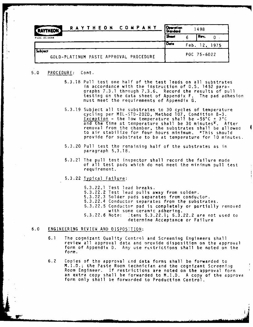
R A Y T H E 0 H C 0 M P A N Y Opw. ionR T O C P s 1498
Fom 20-0044 Shoot 6 R&v. 0
D ; Feb. 12, 1975:-, ubioct
GOLD-PLATINUM PASTE APPROVAL PROCEDURE POC 75-6022
5.0 PROCEDURE: Cont.
5.3.18 Pull test one half of the test leads on all substratesin accordance with the instruction of OS. 1452 para-graphs 7.3.1 through 7.3.6. Record the results of pulltesting on the data sheet of Appendix F. The pad adhesionmust meet the requirements of Appendix G.
5.3.19 Subject all the substrates to 30 cycles of temperaturecycling per MIL-STD-202D, Method 107, Condition B-3.Exception - the low temperature shall be -550 C + 30Cand the time at temperature shall be 30 minutesv. Afterremoval from the chamber, the substrates shall be allowedto air stabilize for four hours minimum. *This shouldprovide for substrate to be at temperature for 10 minutes.
5.3.20 Pull test the remaining half of the substrates as inparagraph 5.3.18.
5.3.21 The pull test inspector shall record the failure modeof all test pads which do not meet the minimum pull testrequirement.
5.3.22 Typical Failure:
5.3.22.1 Test lead breaks.5.3.22.2 Test lead pulls away from solder.5.3.22.3 Solder pads separates from conductor.5.3.22.4 Conductor separates from the substrates.5.3.22.5 Conductor pad is completely or partially removed
with some ceramic adhering.5.3.22.6 Note: tems 5.3.22.1; 5.3.22.2 are not used to
determine Acceptance or Failure
6.0 ENGINEERING REVIEW AND DISPOSITION:
6.1 The cognizant Quality Control and Screening Engineers shallreview all approval data and orovide disposition on the approvalform of Appendix D. Any use rL.trictions shall be noted on theform.
6.2 Copies of the approval E.nd data forms shall be forwarded toM.I.D.; the Paste Room technician and the cognizant ScreeningRoom Engineer. If restrictions are noted on the approval forman extra copy shall be forwarded to M.I.D. A copy of the approvaform only shall be forwarded to Production Control.
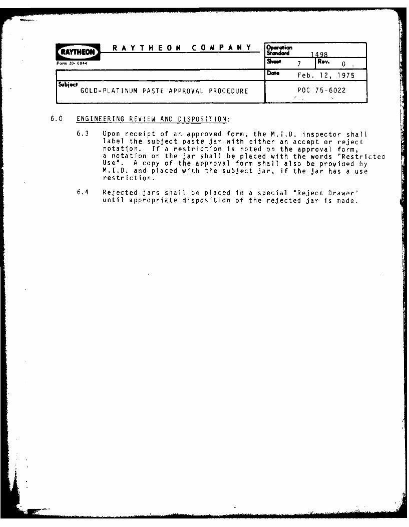
R A Y T H E 0 N C 0 M P A N Y Oeao
Foho 20-00447 Rev. 0Date Feb. 12, 1975
subiectGOLD-PLATINUM PASTE APPROVAL PROCEDURE POC 75-6022
6.0 ENGINEERING REVIEW AND DISPOSITION:
6.3 Upon receipt of an approved form, the M.I.D. inspector shalllabel the subject paste jar with either an accept or rejectnotation. If a restriczion is noted on the approval form,a notation on the jar shall be placed with the words "RestrictedUse'. A copy of the approval form shall also be provided byM.I.D. and placed with the subject jar, if the jar has a userestriction.
6.4 Rejected jars shall be placed in a special "Reject Drawer"until appropriate disposition of the rejected jar is made.
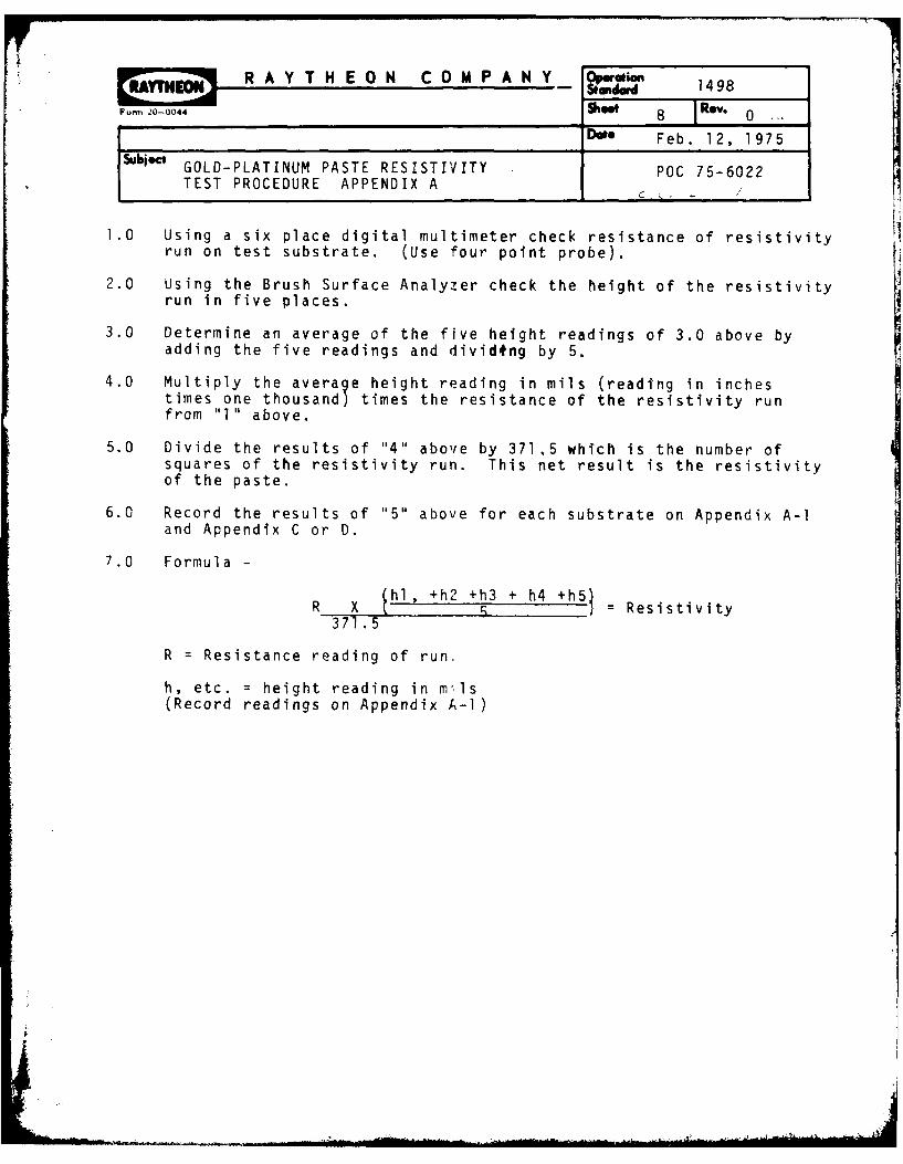
-t
R A Y T H E O N C O M P A N Y O piwa tn= 1498
F.m 20-0044 8 Rev. o
DIt. Feb. 12, 1975
Sibi GOLD-PLATINUM PASTE RESISTIVITY POC 75-6022
TEST PROCEDURE APPENDIX A C i , . /"
1.0 Using a six place digital multimeter check resistance of resistivityrun on test substrate. (Use four point probe).
2.0 Using the Brush Surface Analyzer check the height of the resistivityrun in five places.
3.0 Determine an average of the five height readings of 3.0 above byadding the five readings and dividing by 5.
4.0 Multiply the average height reading in mils (reading in inchestimes one thousand) times the resistance of the resistivity runfrom "I" above.
5.0 Divide the results of "4" above by 371.5 which is the number ofsquares of the resistivity run. This net result is the resistivityof the paste.
6.0 Record the results of "5" above for each substrate on Appendix A-land Appendix C or D.
7.0 Formula -
hl, +h2 +h3 + h4 +h5)R X U' = Resistivity
371.5
R = Resistance reading of run.
h, etc. = height reading in m-ls(Record readings on Appendix A-l)
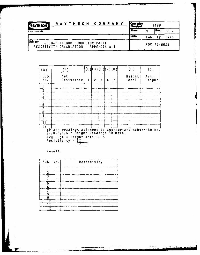
R AY TH EO0N COM P A N Y iu 1498Fonn 20-0044 Show 9 Rev. 0
Do* Feb. 12, 1975
Sbet GOLD-PLATINUM CONDUCTOR PASTE O7562RESISTIVITY CALCULATION APPENDIX A-i1O 562
(A) B)(C)(D)(E)(F)(G) (H) (I)
Sub. Net Height Avg.No. Resistance 1 2 3 4 5 Total Height
2 ____________
23__4_ __ ___
5______
7___
58______
Avg -g =-egt oa - ___
Resistivity BI371 . 5
Result:
1ub No. Resistivity____
23 __________ ___
4 __ _____ _____
5 ___ ___ _____
6 __
7 ______________________
8 ____ ________
9
12__ _ _ __ _ _ _ _ _ _ _ _ _
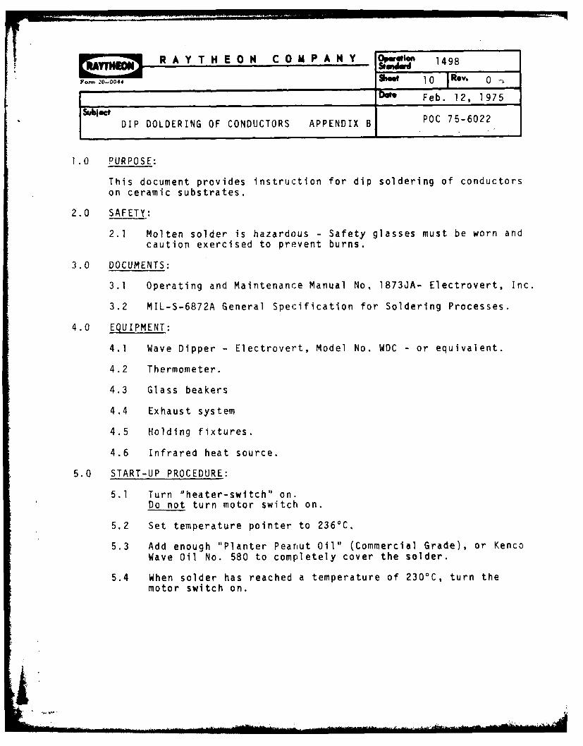
R AY T HEO0N CO0MP A NY oP= 1498
Form 20-0044 w 10 Rev. 0
Daft Feb. 12, 1975
subjectDIP DOLDERING OF CONDUCTORS APPENDIX B POC 75-6022
1.0 PURPOSE:
This document provides instruction for dip soldering of conductorson ceramic substrates.
2.0 SAFETY:
2.1 Molten solder is hazardous - Safety glasses must be worn andcaution exercised to prevent burns.
3.0 DOCUMENTS:
3.1 Operating and Maintenance Manual No, 1873JA- Electrovert, Inc.
3.2 MIL-S-6872A General Specification for Soldering Processes.
4.0 EQUIPMENT:
4.1 Wave Dipper - Electrovert, Model No. WDC - or equivalent.
4.2 Thermometer.
4.3 Glass beakers
4.4 Exhaust system
4.5 Holding fixtures.
4.6 Infrared heat source.
5.0 START-UP PROCEDURE:
5.1 Turn "heater-switch" on.Do not turn motor switch on.
5.2 Set temperature pointer to 236 0 C.
5.3 Add enough "Planter Peanut Oil" (Commercial Grade), or KencoWave Oil No. 580 to completely cover the solder.
5.4 When solder has reached a temperature of 230 0 C, turn themotor switch on.
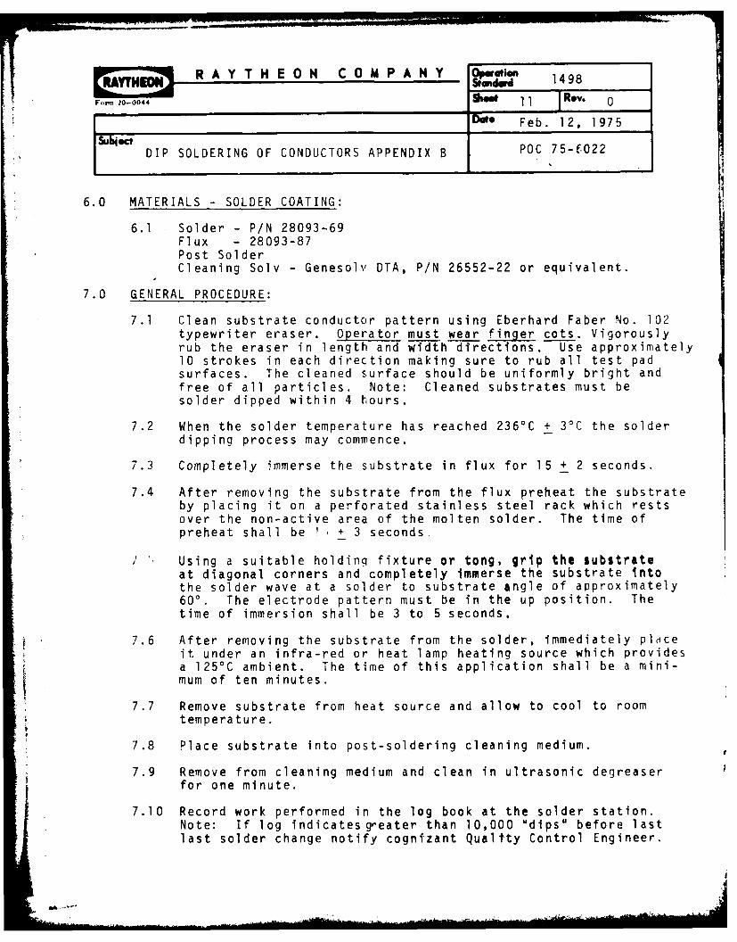
R A Y T H E O N C O M P A N Y O-watinAT Seidwd 1498L 4 .l NJ Sho 9 8
F,,m 20-0044 ee 11 Hy, 0 "
t Feb. 12, 1975abiect f
DIP SOLDERING OF CONDUCTORS APPENDIX B POC 75-CO22
6.0 MATERIALS - SOLDER COATING:
6.1 Solder - P/N 28093-69Flux - 28093-87Post SolderCleaning Solv - Genesolv DTA, P/N 26552-22 or equivalent.
7.0 GENERAL PROCEDURE:
7.1 Clean substrate conductor pattern using Eberhard Faber No. 102typewriter eraser. peprator must wear finger cots. Vigorouslyrub the eraser in length and width directions. Use approximately10 strokes in each direction making sure to rub all test padsurfaces. The cleaned surface should be uniformly bright andfree of all particles. Note: Cleaned substrates must besolder dipped within 4 hours.
7.2 When the solder temperature has reached 236°C + 3C the solderdipping process may commence.
7.3 Completely immerse the substrate in flux for 15 + 2 seconds.
7.4 After removing the substrate from the flux preheat the substrateby placing it on a perforated stainless steel rack which restsover the non-active area of the molten solder. The time ofpreheat shall be + - 3 seconds
S. Using a suitable holding fixture or tong, grip the substrateat diagonal corners and completely immerse the substrate intothe solder wave at a solder to substrate angle of approximately600. The electrode pattern must be in the up position. Thetime of immersion shall be 3 to 5 seconds.
7.6 After removing the substrate from the solder, immediately placeit under an infra-red or heat lamp heating source which providesa 125 0 C ambient. The time of this application shall be a mini-mum of ten minutes.
7.7 Remove substrate from heat source and allow to cool to roomtemperature.
7.8 Place substrate into post-soldering cleaning medium.
7.9 Remove from cleaning medium and clean in ultrasonic degreaserfor one minute.
7.10 Record work performed in the log book at the solder station.Note: If log indicates g-eater than 10,000 udips" before lastlast solder change notify cognizant Qualtty Control Engineer.
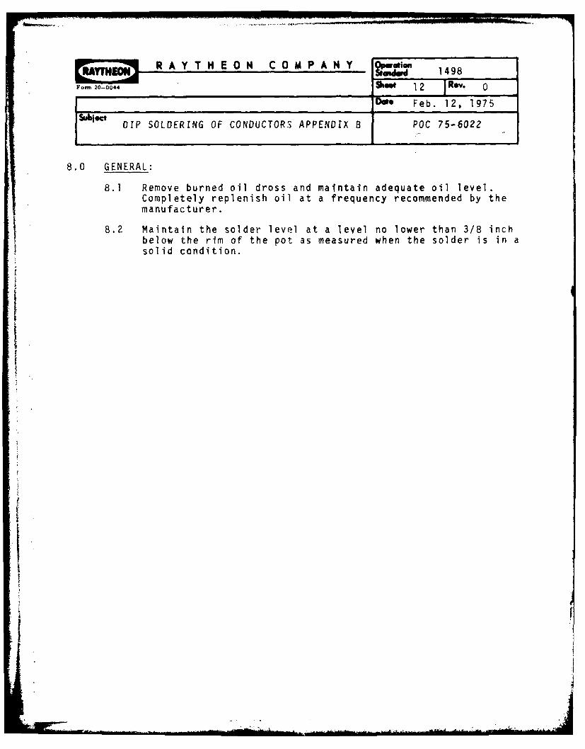
R A Y T H E O N C O M P A N Y O m 1498
Form 20-0044 12 ]Rev. 0
D * Feb. 12, 1975
DIP SOLDERING OF CONDUCTORS APPENDIX B POC 75-6022
8.0 GENERAL:
8.1 Remove burned oil dross and maintain adequate oil level.Completely replenish oil at a frequency recommended by themanufacturer.
8.2 Maintain the solder level at a level no lower than 3/8 inchbelow the rim of the pot as measured when the solder is in asolid condition.
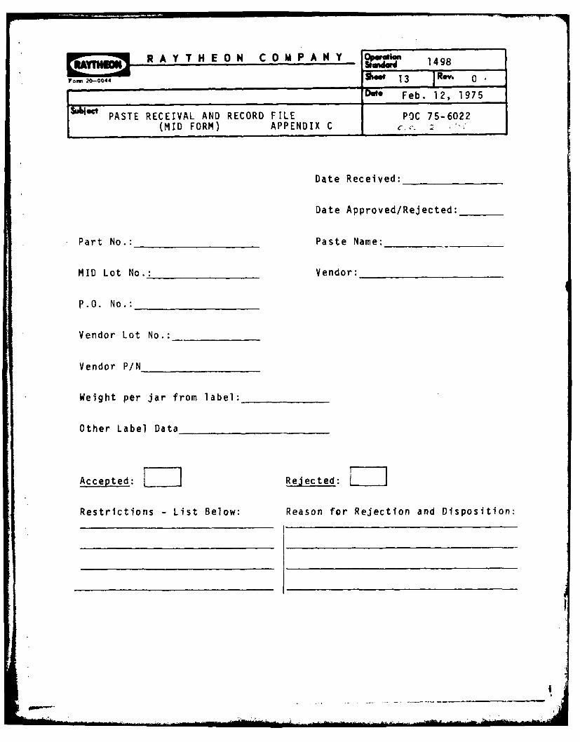
Formi 20-0044 Shw 13 Rev. 0
Do* Feb. 12) 1975
&Modsc PASTE RECEIVAL AND RECORD FILE P')C 75-6022
(MID FORM) APPENDIXC
Dote Received:_________
Date Approved/Rejected: ____
Part No.: ___________Paste Name; __________
MID Lot No.: Vendor:_____________
P.O. No.: ___________
Vendor Lot No.:________
Vendor P/N__________
Weight per jar from label: _______
Other Label Data______________
Accepted: Rejected: ERestrictions -List Below: Reason for Rejection and Disposition:
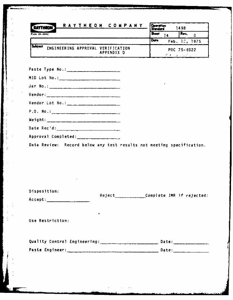
Foom 20-0044 5~Sho 4 Rv_________________________________Deft_ Feb.__l2,__1975
SbetENGINEERING APPROVAL VERIFICATION POC 75-6022APPENDIX D
Paste Type No.: ___________
MID Lot No.:__ _ _ _ _ _ _ _ _ _ _
* - Jar No.:__ _ _ _ _ _ _ _ _ _ _ _ _
Vendor.: _ _ _ _ _ _ _ _ _ _ _ _ _ _ _
Vendor Lot No.:____ _______
P.O. No.:_ _ _ _ _ _ _ _ _ _ _ _ _
Weight: _ _ _ _ _ _ _ _ _ _ _ _ _ _ _ _
* Date Rec'd: _ _ _ _ _ _ _ _ _ _ _ _ _
Approval Completed:
Data Review: Record below any test results not meeting specification.
DioiS S1ti on:Reject Complete IMR if rejected:
Accept:_______ ___
Use Restriction:
Quality Control Engineering: _____________Date: _______
Paste Engineer: _____________________Date: ________
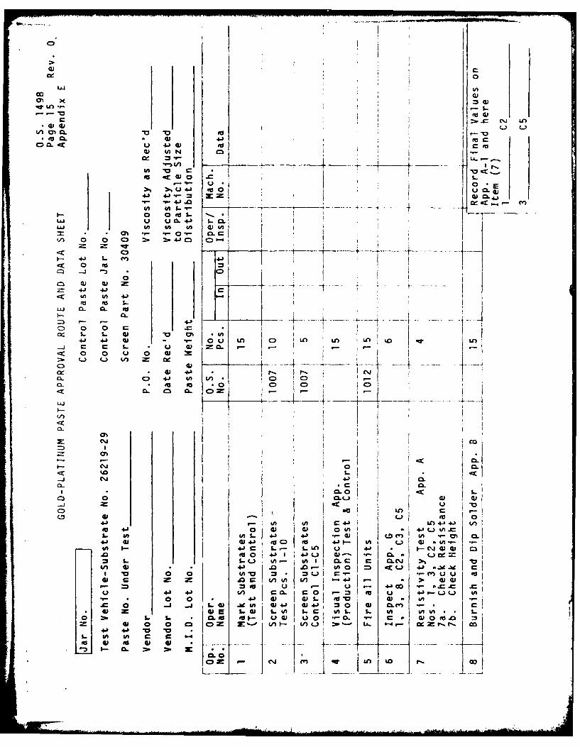
L..J
Om x
.0101 C.)1.
> u 4.) 0) to.i
to 44 ~ 0 S
1 4U 4-) 0E41 4.). Im 06
(A fA I-v
LW w too IA i
V)~U Cl > w) C) WC)
F- 4-) ~) 4 jI
-j -C*0-n->l* I- -
4J 443
Lij c00__'
o 4J (n CDlto M a .0 C0 C)
-0 m
CL m). )(.()~
.0 'aXL3 . C.)Z Qi
cz LL LLa 0)- IS 0 C .'J4J 0 *4 In .0. r-C 41 LO 43 4
*0 4J 0 0 V)) 4J W 0L) M '(
V- w 4J .0 .0 # 0 U 4J -L)CJ -U )
0C 0 43 %- 01 Ioi 01. CA
0 10L. L 0L~o .fif 01 u43 04 -, 13. 01 0.E.0
C)
co
.1l
too C3
CD a-.-C
o Il
z -c
4--I
0 - u O (-) LO L
C-4 C%%4 IV
I cn
CCDG
o D av W 40 - C- a0 Ui
39c; go ' eJ Lgo 9-'r_ K u
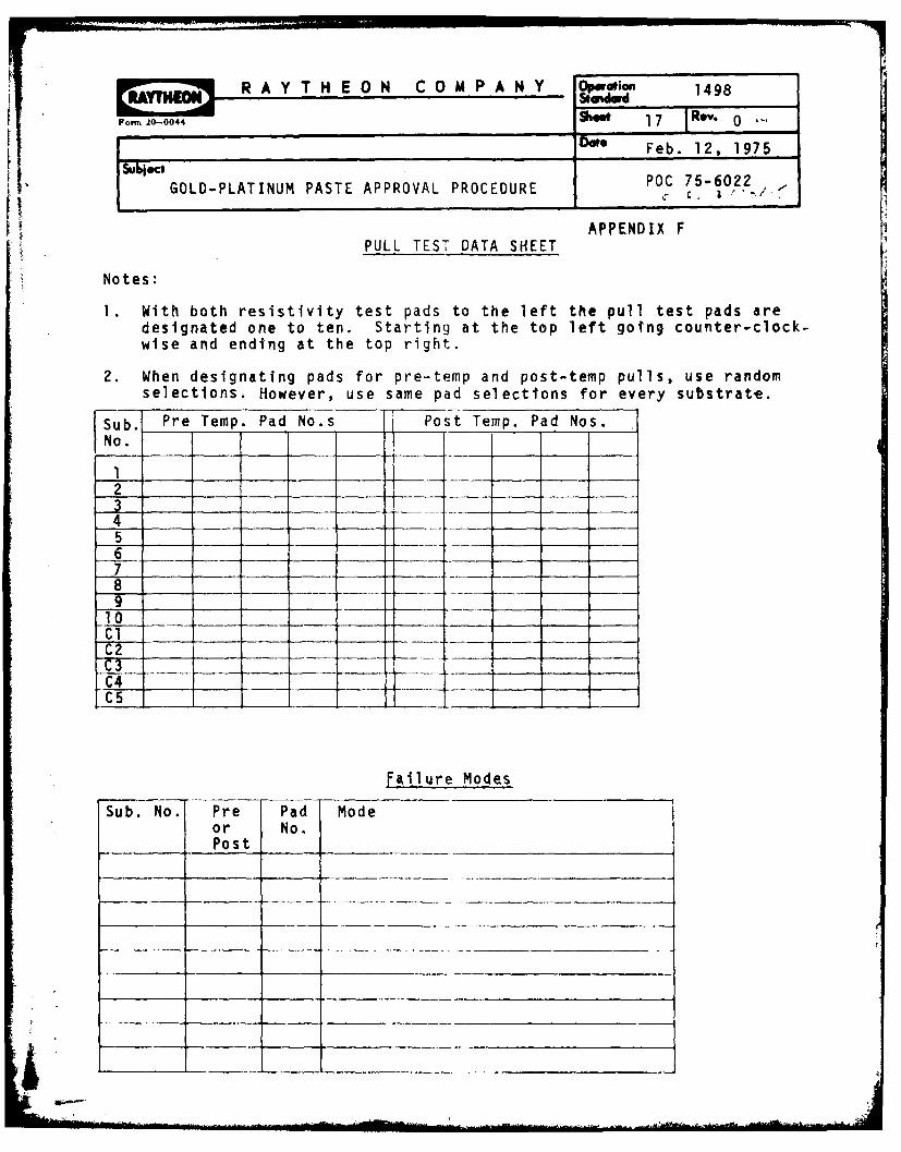
RAY HEO COMPAN Wr 1498
Form 20-0044 So 17 Rev. 0
De Feb. 12, 1975
GOLD-PLATINUM PASTE APPROVAL PROCEDUREPO 7562
APPENDIX FPULL TEST1 DATA SHEET
Notes:
1. With both resistivity test pads to the left the pull test pads aredesignated one to ten. Starting at the top left going counter-clock-wise and ending at the top right.
2. When designating pads for pre-temp and post-temp pulls, use randomselections. However, use same pad selections for every substrate.
Sub. Pre Temp. Pad No.s PostTemp.__Pad Nos.
N ol____________ ____________ ___________ ___________ ___________ _________ __________ ___________ ____________ ____________
1 __________ _____ _____ __________
2 ______ _ _ __ ___ ___ __
43__ ___ __
4 ___ ___ ___ ___ ___
65___ ___ __ ___ ___
7 6__ ___ ___ ______ ___ ___
7 ___ ___ _ _
98 ___ ___ ______
10 __ _ _ _ ____ __ _ __ _ _ _
Cl 1 _ _ ____ _ __ _ _
Fallure Modes
Sub. No. Pre Pad Modeo r No.
____ ____ Post _ _ _ _ __ _ _ _ _ _ _ _ _ _ _ _ _
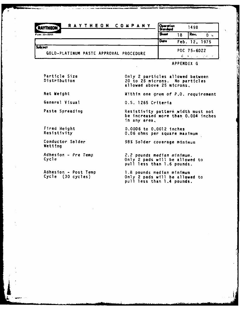
R A Y T H E O N C 0 M P A N Y Operion 1498
Form, 20-0044 Shw 18 Rev. 0Date Feb. 12, 1975ISui hC POC 75-6022
GOLD-PLATINUM PASTE APPROVAL PROCEDURE
APPENDIX G
Particle Size Only 2 particles allowed betweenDistribution 20 to 25 microns. No particles
allowed above 25 microns,
Net Weight Within one gram of P.O. requirement
General Visual O.S. 1265 Criteria
Paste Spreading Resistivity pattern ,width must notbe increased more than 0.004 inchesin any area,
Fired Height 0,0006 to 0,0012 inchesResistivity 0,06 ohms per square maximum
Conductor Solder 98% Solder coverage minimumWetting
Adhesion - Pre Temp 2.2 pounds median minimum.Cycle Only 2 pads will be allowed to
pull less than 1.6 pounds.
Adhesion - Post Temp 1.8 pounds median minimumCycle (30 cycles) Only 2 pads will be allowed to
pull less than 1.4 pounds.
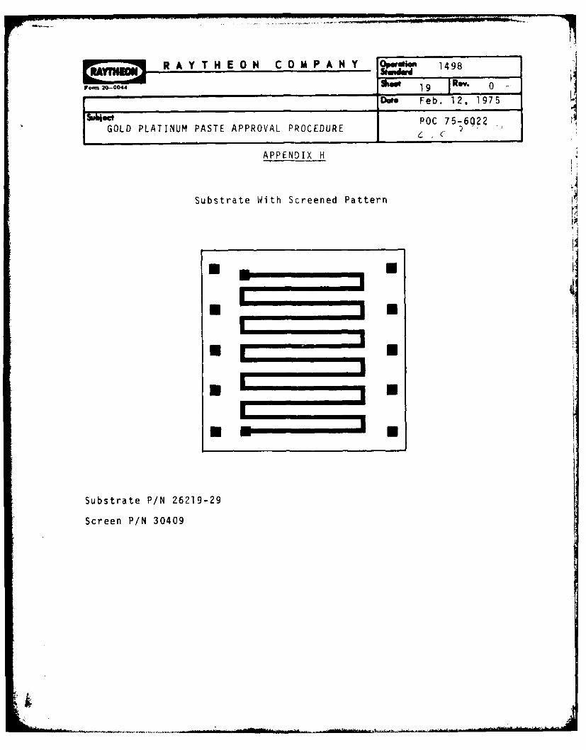
R AY TH EO0N CO0M P A NY ~~1498
Fonm 20-0044 i Re. 0
GOLD PLATINUM PASTE APPROVAL PROCEDURE 7-O?6.C
APPENDIX H
Substrate With Screened Pattern
Substrate P/N 26219-29
Screen P/N 30409
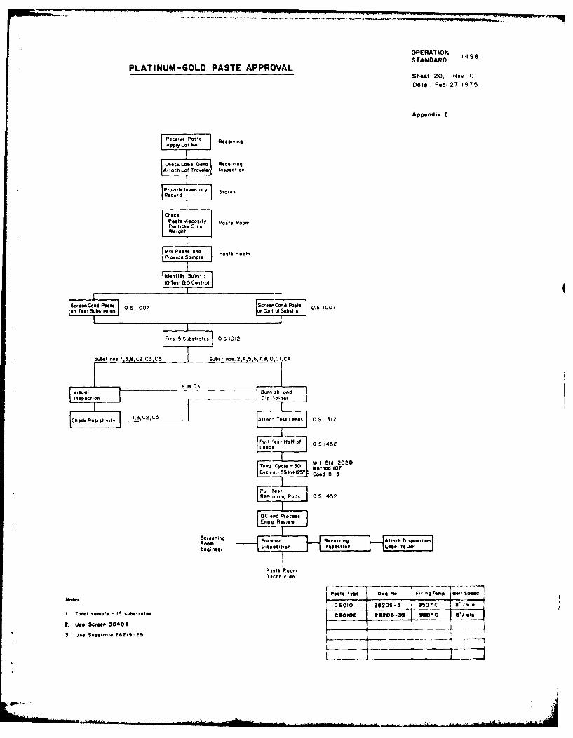
OPERATION 1498STANDARD
PLATINUM-GOLD PASTE APPROVALSheet 20. Rev 0
Dote Feb. 27, 1975
Appendix I
Receve Pst. Receiving
Ctreh Lbel ata ReceivingAttat, ot ravle instpection
Provide lesentor, StoresRecord
Posteviscoa Paste RoomParticle SizeWeight
1011 Paste and posts Room
or ov do Sample
Fideetify S-.t'10OTell-8 a ro
ScrenCottd Past 0 S 1007 ScreevCond. Poll. 0.5 1007
Subsrat4*0an o~tr~ol Subst's
Subst nlos 1,3,8,C2 C5 C5 subt nas.2 4,5,6,7,910 CI C4
Chec Resstivty ",C2,5 AtaiTo sl Leads 0S 1312
Pl etHolt 0' 0 S 1452
T~mtCycl -~ Mil-Std-202DTemf ycle_ 30 Method 107CVI-55t04l25a' Coed B -
RmogPods OS 1452
OC rd FProcess
'nginger clB osilon leepectioc Label to Ja
P~ste Roo.T c he~c,a,
Paste Type I Owe Na Firing Tomp- 00e Speoe47
Notes I-C6010 2205-3 950"' C am
Itotal Sample - is 0subltrot igoo9 NOOC 6fmij
2. Use Screen 30409
3Use Substrate 282 19-29
SR A Y T H E O N C O M P A N Y Operatiok.mdwd 1500
Ponn 20-0044 Shoe 1 Re 1SDate March 19, 1976
RESISTOR PASTE APPROVAL PROCEDURE POC 76-6063
1.0 Purpose
This procedure details the steps for approval of resistor paste used onthick film microelectronic substrates.
2.0 Scope
This procedure provides instruction for the handling, processing, and test-ing of resistor paste material from the time of receival to final evaluationand disposition. Tests include particle size distribution, resistivity,interface resistivity, TCR and visual criteria.
3.0 Documents
Drawing No. 29468O.S. 1005 - Resistor Paste Approval0.S. 1007 - Electrode ScreeningO.S. 1008 - Screening ResistorsO.S. 1009 - Resistor FiringO.S. 1012 - Firing Profiles, Chatacteristics, Freq.O.S. 1039 - Temp. Coefficient Test ProcedureO.S. 1450 - Qual, Procedure for the Honeywell Substrate ProgramO.S. 1475 - Particle Size DistributionO.S. 1487 - Res. Paste Stati'c Electricity Shift
4.0 Equipment, Tooling, Gauges
4.1 Prescco Screener or equivalent
4.2 Set of screens 29469, 29470
4.3 Conveyor dryer 110 - 120 0C
4.4 W. J. resistor furnace
4.5 W. J. conductor furnace
4.6 Hewlett Packard 3440A digital voltmeter
4.7 Substrate marking pencil
4.8 Surfanalyzer
4.9 3KV Power Supply
4.10 Test box for static charge shift test
4,11 Stero zoom microscope lOX - 30X with backllghting capability
1 2 3 4 5 6 7 8 9 10 11 12 13 14 15
00 000000000000 00
R A Y T H E O N C O M P A N Y O 1500
,o 20-0044 Sk9 2 Rev. 0
Date 5/8/75subioct
Resistor Paste Approval Procedure
5.0 Procedure
5.1 Receipt of Paste from Vendor
5.1.1 NO delay shall be allowed in the handling of gold paste materialsfrom receipt of paste until delivery to Stores.
5.1.2 The Material Inspection Dept. shall review paste label data for con-formance with purchase order requirements.
5.1.3 The label data shall be recorded on an appropriate data sheet alongwith received date, lot no. and issue date to Stores. (See Appendix B)
5.1.4 If any discrepancies are noted during this examination, the cognizantQuality Control Engineer shall be consulted for disposition of thematerial.
5.1.5 A paste approval data form (Appendix D) shall be forwarded with thelot to Stores.
5.1.6 Store room personnel shall record pertinent information on inventoryrecords and forward the paste to the "Paste Room" on the same day.
5.1.7 Paste room personnel shall record the receival of the paste and main-
tain segregation and security of the unapproved material.
5.2 Paste Room Sampling and Analysis
5.2.1 The paste room technician shall check and record:paste viscosity, net weight and particle size distribution.Refer specification sheet of Appendix G.
5.2.1.1 Paste viscosity shall be checked using the Roto-Visco Unit accordingto O.S. 1034.
5.2.1.2 Net weight of paste shall be measured to the nearest gram. A standard weightfor the container and cover shall be assumed.
5.2.1.3 Particle size distribution shall be measured in accordance with O.S. 1475.
5.2.1.4 If lots are rejectable to net weight and/or particle size distributioncriteria, disposition of the lot shall be made prior to continuance oflot approval.
~~~R A Y T H E 0 N C 0 M P A N Y OliR Y E CN 7 1500
Fono 20-0044 R3"
SDac 5/8/75+ Subgect
Resistor Paste Approval Procedure
~5.0 Cont.
5.2.2 Paste Sampling for Paste Approval:
5.2.2.1 The paste technician shall mix the paste with a clean spatula forten minutes.
5.2.2.2 Approximately one to two ounces shall be transferred to a 1 fl. ounceplastic jar provided for testing purposes. The weight of the sampleshall be recorded in the material usage log book. Paste sample shallbe properly identified.
5.2.2.3 The paste sample shall be delivered to the paste approval screening
technician with the data form of Appendix D.
5.3 Screening of Sample Substrates
NOTE: All process and test/inspection data must be recorded on the traveller.Appendix
5.3.1 Paste Types
5.3.1.1 Refer to flow diagram of Appendix for applicable paste types.
5.3.2 Substrate Test Vehicle - Use substrate P/N 26219-29.
5.3.3 Clean substrates per O.S. 1000.
5.3.4 Marking - Using an aluminum marker identify the reverse side of eachsubstrate with the numbers "1"; "2"; and "3".
5.3.5 Conductor Screening - Using a fully approved C6010 conductor material(P/N28205-3or 39) screen the pattern of screen No. 29469 on thethree substrates. (Refer O.S. 1007)
5.3.6 Fire the 3 substrates per O.S. 1012. The fired height must be between.0006" to .0012".
5.3.7 Screen the resistor paste under test using screen no. 29470.Refer O.S. 1008
5.3.8 Fire the screened substrates per O.S. 1009
The fired resistor height must be between .006" to .0012".
5.3.9 Deliver the three samples and documentation to the inspection department.
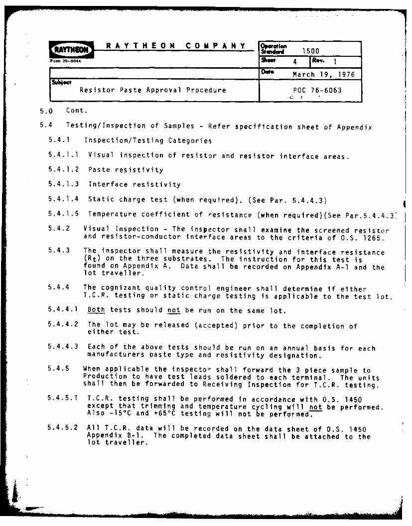
R A Y T H E O N C O M P A N Y O#pgwlw 1500
Foon 20-0044 s 4 Rv. ID___ March 19, 1976
Resistor Paste Approval Procedure POC 76-6063
5.0 Cont.
5.4 Testing/Inspection of Samples - Refer specification sheet of Appendix
5.4.1 Inspection/Testing Categories
5.4.1.1 Visual inspection of resistor and resistor interface areas.
5.4.1.2 Paste resistivity
5.4.1.3 Interface resistivity
5.4.1.4 Static charge test (when required). (See Par. 5.4.4.3)
5.4.1.5 Temperature coefficient of resistance (when required)(See Par.5.4.4.3'
5.4.2 Visual Inspection - The inspector shall examine the screened resistorand resistor-conductor interface areas to the criteria of O.S. 1265.
5.4.3 The inspector shall measure the resistivity and interface resistance(Rt) on the three substrates. The instruction for this test isfound on Appendix A. Data shall be recorded on Appendix A-l and thelot traveller.
5.4.4 The cognizant quality control engineer shall determine if eitherT.C.R. testing or static charge testing is applicable to the test lot.
5.4.4.1 Both tests should not be run on the same lot.
5.4.4.2 The lot may be released (accepted) prior to the completion ofeither test.
5.4.4.3 Each of the above tests should be run on an annual basis for eachmanufacturers paste type and resistivity designation.
5.4.5 When applicable the inspector shall forward the 3 piece sample toProduction to have test leads soldered to each terminal. The unitsshall then be forwarded to Receiving Inspection for T.C.R. testing.
5.4.5.1 T.C.R. testing shall be performed in accordance with O.S. 1450except that trimming and temperature cycling will not be performed.Also -15'C and +650 C testing will not be performed.
5.4.5.2 All T.C.R. data will be recorded on the data sheet of O.S. 1450Appendix B-l. The completed data sheet shall be attached to thelot traveller.
.d
R A Y T H E 0 N C 0 M P A N Y 150
Form 20-0044 1940 5 -jRev. 0
Do* 5/8/75
Resistor Paste Approval Procedure
5.0 Cont.
5.4.6 When applicable, the inspector will test the sample for static voltageapplication in accordance with O.S. 1487. The data *ill be recordedon Appendix C.
5.5 Engineering Review and Disposition
5.5.1 The cognizant Quality Control and Screening Engineers shall review allapproval data and provide disposition on the approval form of Appendix E.Any use restrictions shall be noted on the form.
5.5.2 Copies of the approval and data forms shall be forwarded to M.I.D.; thePaste Room technician, and the cognizant Screening Room Engineer. Ifrestrictions are noted on the approval form an extra copy shall be for-warded to M.I.D. A copy of the approval form only shall be forwardedto Production Control.
5.5.3 Upon receipt of an approved form, the M.I.D. inspector shall label thesubject paste jar with either an accept or reject notation. If arestriction is noted on the approval form, a notation on the jar shallbe placed with the words "Restricted - Use". A copy of the approvalform shall also be provided by M.I.D. and placed with the subject jar,if the jar has a use restriction.
5.5.4 Rejected jars shall be placed in a special "Reject Drawer" untilappropriate disposition of the rejected jar is made.
I
@ON A T HE 0H ' 0 MP AH Y1500i l1 R e,"
Foim 20-0044 So 60l ' ~ee' 5/8/75
Resistor Paste Approval Procedure POC 75-6103
APPENDIX A
Resistivity Test Procedure
1.0 This Appendix provides instruction for the determination of resistivityand interface resistance (Rt).
2.0 Note: A total of 30 height readings and 30 resistance readings will be
taken. Each of the 3 substrates contains 5 "1" square and 5 - "2" squareresistors.
3.0 Using a six place digital multimeter, check the resistance of eachresistor and record results on the data sheet of Appendix A-1.
4.0 Using the Brush Surf Analyzer check the height of each resistor andrecord results on the data sheet of Appendix A-1.
5.0 Multiply each height reading in mils (reading in inches times 1000)
times its respective resistance reading in ohms. Record this calculationon the data sheet of Appendix A-1.
6.0 Add the calculated results from paragraph 5.0 for "I" square resistorsand "2" square resistors. Record these two totals on the data sheetof Appendix A-1. As a matter of convenience the total of "1" squareresistor calculations shall be called "B"; and the total of "2" squareresistor calculations shall be called "A".
7.0 Resistivity can now be calculated using the formula.
Resistivity A B (answer is in ohms/square)15 15
Record results on data sheet.
8.0 Rt can now be calculated using the formula.Bt
Rt - Resistivity (answer in ohms)
R 15
Record results on data sheet
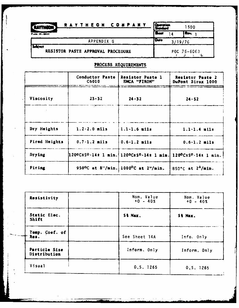
IIAYIION R A Y T N E 0ON C 0 M P A N YE ml 500
,o 0-0044 14 10".
APPENDIX G Do* 3/19/76
RESISTOR PASTE APPROVAL PROCEDURE POC 76-60C3I _ _ __ _ __ _I C
PROCESS REQUIREMENTS
Conductor Paste Resistor Paste 1 Resistor Past. 2C6010 E4CA "PIRON" DuPont Birox. 1000
Viscosity 23-32 24-32 24-S2
Dry Heights 1.2-2.0 mils 1.1-1.6 ails 1.1-1.4 mils
Fired Heights 0.7-1.2 ails -0.6-1.2 ails 0.6-1.2 ails
Drying 120oCSO-14t 1 rmin. 120oCtSO-14t 1 main. 1200CtS°-14t 1 ruin.
Firing 9SOOC at 8"/min. 10000 C at 2"/min. 850C at 2A/min.A
Resistivity Nom, Value Nom. Value+0 - 40% +0 - 40%
Static Elec. St Max. St Max.Shift
......Temp. oejf. of" Res. See Sheet 14A Info. Only
Particle Size Inform. Only Inform. OnlyDistribution
Visual O,S. 1265 O,S. 1265
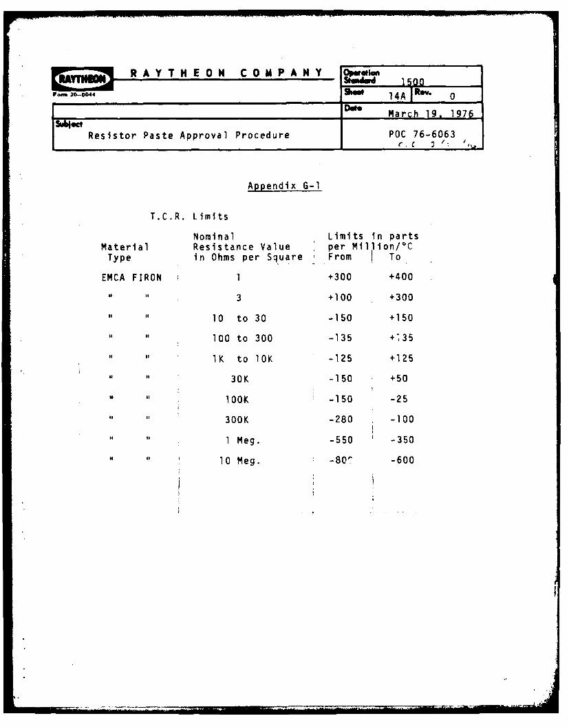
Foum 20-004414AIRv 0f Resistor Paste Approval Procedure POC 76-6063
Appendix G-1
T.C.R. Limits
Nominal Limits in partsMaterial Resistance Value per Mlllion/OCType in Ohms per Square From IToEMCA FIRON 1 +300 +400
H it 3 +100 +300
10 to 30 -150 +150
100 to 300 -135 +-.35
1K to 10K -125 +125
U I30K -150 +50
100K -150 -25
It300K -280 -100
1 Meg. -550 -350
10 Meg. -80',' -600
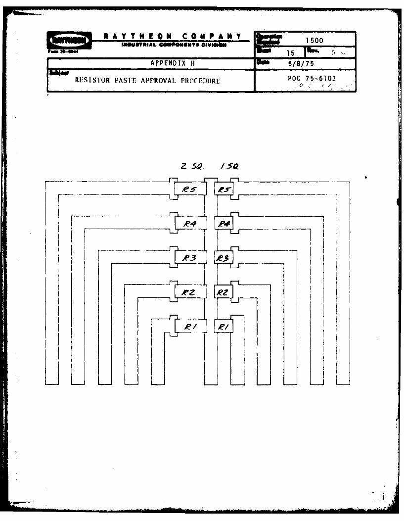
M A~Q Y5 T S MPANY10
____MIA ___"NT £5 - - -
~*t f40
A PENI H £3187
PC 75210
R E S I S T O P A S T A P R VL iRC D U EC
kp .3'
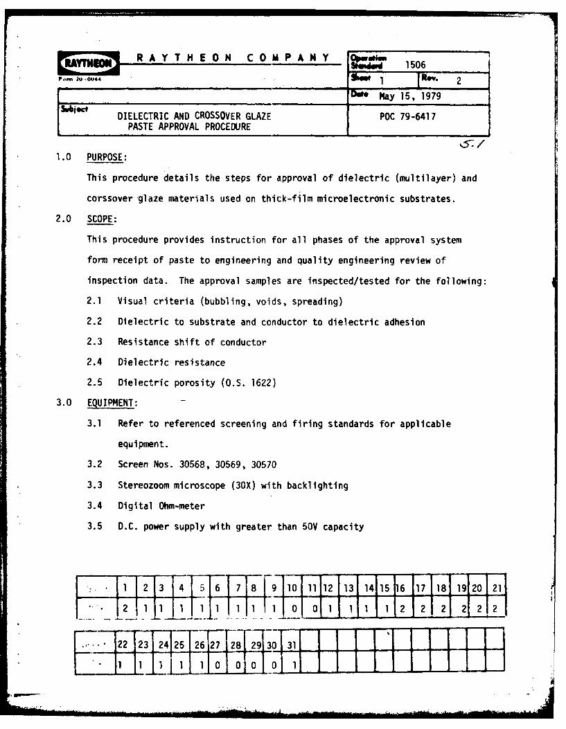
RAYTHEON COMPANY 1506
,,.oo1 Re, taw. 2_ _ _ __M May 15, 1979
M DIELECTRIC AND CROSSOVER GLAZE POC 79-6417PASTE APPROVAL PROCEDURE
1.0 PURPOSE:
This procedure details the steps for approval of dielectric (multilayer) and
corssover glaze materials used on thick-film microelectronic substrates.
2.0 SCOPE:
This procedure provides instruction for all phases of the approval system
form receipt of paste to engineering and quality engineering review of
inspection data. The approval samples are inspected/tested for the following:
2.1 Visual criteria (bubbling, voids, spreading)
2.2 Dielectric to substrate and conductor to dielectric adhesion
2.3 Resistance shift of conductor
2.4 Dielectric resistance
2.5 Dielectric porosity (O.S. 1622)
3.0 EQUIPMENT:
3.1 Refer to referenced screening and firing standards for applicable
equipment.
3.2 Screen Nos. 30568, 30569, 30570
3.3 Stereozoom microscope (30X) with backlighting
3.4 Digital Ohm-meter
3.5 D.C. power supply with greater than 50V capacity
! -- 1i 1 1,-1. 2 3I45 7 910 11 12 13 14 15 16 17 18 19 20 212 11 111 1 0 0 1 1_[ 1 222 222
22 23 24 25 26 27 28 291 31
I I 1 1 0 0
R A Y T H E O N C O 14 P A N Y OpeatioiSimdwd 1506
, - .. .... Sh oe w 2 | R e v.
Date September 20. 1977subiect DIELECTRIC AND CROSSOVER GLAZE POC 77-6344
PASTE APPROVAL PROCEDURE
3.0 EQUIPMENT: Cont.
3.6 Particle size analysis wedge.
3.7 Diamond scribe (Phono-point diamond tip).
3.8 Rotovisco viscosity analyzer.
4.0 DOCUMENTATION:
See referenced specifications.
5.0 PROCEDURE:
5.1 Receipt of paste from vendor:
5.1.1 The Material Inspection Dept. shall review paste
label data for conformance with purchase order require-
ments.
5.1.2 The label data shall be recorded on an appropriate
data sheet along with received date, lot no. and
issue date to Stores. (See Appendix B)
5.1.3 If any discrepancies are noted during this examina-
tion, the cognizant Quality Control Engineer shall
be consulted for disposition of the material.
5.1.4 A paste approval data form (Appendices C & C) shall
be forwarded with the lot to Stores.
5.1.5 Store room personnel shall record pertinenet infor-
mation on inventory records and forward the paste
to the "Paste Room" on the same day.
5.1.6 Paste room personnel shall record the receival of
the paste and maintain segregation and security of
unapproved material.
R A Y T H E 0 N C 0 14 P A N Y OperationE E -sadard 1506
3 1Date Sevtember 20, 1977
ubiect DIELECTRIC AND CROSSOVER GLAZE
PASTE APPROVAL PROCEDURE pOC 77-6344
5.0 PROCEDURE: Cont.
5.2 Paste Room Sampling and Analysis:
5.2.1 The paste room technician shall check and record:
paste viscosity, net weight, and particle size
distribution. Refer specification sheet of Appen-
dix G.
5.2.1.1 Paste viscosity shall be checked using the Roto-
Visco Unit according to O.S. 1034.
5.2.1.2 Net weight of paste shall be measured to the near-
est gram. A standard weight for the container and
cover shall be assumed.
5.2.1.3 Particle size distribution shall be measured in
accordance with O.S. 1475.
5.2.1.4 If lots are rejectable to net weight and/or particle
size distribution criteria, disposition of the lot
shall be made prior to continuance of lot approval.
5.2.2 Paste Sampling for Paste Approval:
5.2.2.1 The paste technician shall mix the paste with a
clean spatula for ten minutes.
5.2.2.2 Approximately one to two ounces shall be trans-
ferred to a 1 fl. ounce plastic jar provided for
testing purposes. The weight of the sample shall
be recorded in the material usage log book. Paste
sample shall be properly identified.
rATIFM R A Y T H E 0 N C 0 14 P A N Y Op 7i 50COIPAN Stid4 1506
I- .. ... " 144 Rev.4 1Dw.September 20, 177
s ub i e t 9 7DIELECTRIC AND CROSSOVER GLAZE POC 77-634
PASTE APPROVAL PROCEDURE
5.0 PROCEDURE: Cont.
5.2.2.3 The paste sample shall be delivered to the paste
approval screening technician with the data forms
of Appendices C, D and E.
5.2.2.4 During the mixing procedure or at any other stage
of paste sampling, the technician shall assure that
no visible contamination is present. if contamina-
tion is found the test shall be stopped and the
cognizant Q.C. Engineer notified.
5.3 Screening and Inspection Procedure For Dielectric Used
In Multilayered Substrates.
NOTE: Referenced O.S.'s pertaining to screening, drying, and firing
are for reference only. Schedules with respect to temp-
erature and speed as found on the flow diagram will supersede.
5.3.1 Clean sixteen (16) substrates per O.S. 1000. Use
substrate P/N 26219-29.
5.3.2 Mark eight (8) substrates with numbers 1 to 8 and 8
substrates with numbers Cl to C8.
5.3.3 Using the dielectric under test, screen substrates
1 through 8 using screen number 30568. Refer O.S. 1010.
5.3.4 Allow the screened substrates to dry at room ambient
conditions for 10 minutes.
_R A Y T H E 0 N C 0 14 P A N Y Opweriof.AC kodrd 1506
F M"W 5 1Rev.1Date September 20, 197
subioct DIELECTRIC AND CROSSOVER GLAZE
PASTE APPROVAL PROCEDURE POC 77-6344
5.0 PROCEDURE: Cont.
5.3.5 Radiant dry thescreened substrates using the belt
dryer. Refer flow diagram. (Appendix H-2)
5.3.6 Fire the test samples in accordance with the flow
diagram of Appendix H-2. (Refer O.S. 1010).
5.3.7 Under 30X magnificationusing a stereozoom microscope
with backlighting, check for visual and dimensional
criteria per Appendix G. The microscope should con-
tain a reticule for dimensional inspection.
5.3.8 Rescreen the pattern of P/N 30568 and follow the
steps of paragraph 5.3.3 through 5.3.5. (Screening
through Radiant Drying).
5.3.9 Perform dimensional check only as in paragraph 5.3.7.
5.3.10 Fire the test samples in accordance with the flow
diagram of Appendix H-2. (Refer O.S. 1010).
5.3.11 Under 30X magnification, using a stereozoom micro-
scope with backlighting, check for visual and dim-
ensional criteria per Appendix G. The microscope
should contain a reticule for dimensional inspection.
5.3.11.1 Remove six (6) substrates (6,7,8 and C6,C7, C8) for
dye check of porosity per O.S. 1622. Record results
in the data column of the routing sheet. (App.D)
rtATM R AY T H EON COMJdP A NY 0Opwian= 1506
S Rev.D September 20, 1977
subiect DIELECTRIC AND CROSSOVER GLAZE
PASTE APPROVAL PROCEDURE POC 77-6344
5.0 PROCEDURE: Cont.
5.3.12 Using a previously approved dielectric paste of the
same type as the paste under test, perform all screen-
ing drying, firing and inspection operations on sub-
strates Cl-C8 (Control) following the instructions of
paragraphs 5.3.3 through 5.3.11 inclusive.
5.3.13 Screen and dry the applicable gold conductor materialon tcn (10) substrates (1-5 and Cl-C5) using screenNo. 30569.
NOTE: The gold screened conductor must be allowed to air
dry for fifteen (15) minutes at room ambient con-
ditions prior to radiant (belt) drying. Refer pic-
torial of Appendix F-2.
5.3.14 Fire all ten (10) substrates per the schedule on the
flow diajram of appendix H-2. (References: O.S. 1007
and 1012).
5.3.15 Inspect visually for bubbling and voids on the elec-
trode surface in accordance with the specification
of Appendix G. (10 substrates)
5.3.16 Fire substrates 1,2, Li and C2 thirteen (13) times
per the schedules on the flow chart of Appendix H-2.
.. 17 Check substrates 1,2, Cl and C2 for bubbling and
voids as in paragraph 5.3.15.
4 check substrates 1,2, Cl and C2 for conductor and die-
-,ric- adhesion in accordance with the instruction
kipendix A and the specification of Appendix G.
rlAT "4 R A Y T H E 0 N C 0 A4 P A N Y ,,i1*
Sbji t Dco* September 20, ' 1977
DIELECTRIC AND CROSSOVER GLAZE
PARTE APPROVAL PROcEnTIRE _P_ 77-644
5.0 PROCEDURE: Cont.
5.3.19 Seal substrates 1,2, Cl and C2 in an envelope and
attach to the lot traveler.
5.3.20 Check substrates 3,4,5,C3,C4, C5, for electrode
resistance. Record data on Appendix E.
5.3.21 Rescreen test dielectric on substrates 3,4,5 and the
control dielectric on substrates C3,C4 and C5,
using screen no. 30568. Follow the instructions of
paragraphs 5.3.3 through 5.3.12 inclusive except
that no dimensional inspections will be made.
PLEASE NOTE: After these screenings, the six (6) substrates should
have two (2) dielectric screenings; one gold screen-
ing followed by two (2) dielectric screenings.
5.3.22 Check substrates 3,4,5,C3,C4, and C5 for electrode
resistance. Record data on Appendix E. Determine per-
cent resistance shift for each substrate.
5.3.23 Screen and dry the second electrode using the appli-
cable gold paste and screen P/N 30570 on the six (6)
substrates.
NOTE: Gold screened conductor must be allowed to air dry for
fifteen (15) minutes at room ambient conditions prior
to radiant (belt) drying. Refer pictroial of
Appendix F-4, Reference O.S. 1007.
o 0 . - S.a
N c ., r_In01 O -,~ to .0- W a
S4-) 0..4J
41 I
#A S.. in'a(
* . 9-4-
-cc 1 _ _ 1
cc 4 4 1 .
C 00 'u 0
cx 4- C E 044V wC1
-J
CL
L*J .4 L
M n ri O 0 0 00 0 0 01 0 rGD 4) 0 C I0
.0 C) CL.r
CSI
wO 4A. w 0 FA #A $A004 U
4U 4 54. W0 4J U . 00 1-'4 - 0 0 -J-'-,0a 0 o .. to vo L&. r. ro 4A
0-1 0 *0 CM 4* 0 04J W P- 0~ 4J *r CC -o 1.L 4.I1a . c 4V fW4 oI .4 e cC
InI
4) jcm*I
ld CL 41C, CLc
II I
-
to 0
w 4.)
r
CD
U ------- ----
4) w o 'W Iz
CL U' LO cl0 0.L
C3 u 0 0 CD CL C - C
-J 0 E-j >) C14IL to 0' CA , ~.
4A o 0- V).- Uva; r- U) >)r p 4A S 41 a)4- 4
o 4)I 4-) 1 4J~U 4 4J W S o 0 u - oto im .lE- 0 1 4 ~ E
4-2 0 S- rI - m S- 4-44- o) 4J im 0) w 4- in0 V-0 IA U)4J #
-J c 0 CL in U,. a 4 C 04J a c~O'
Io o C L )- )t 1 _u+j1. ( ULUGV 4-J (U eq
ro .4 a) 0 V4)
'
04. LA_ V) 0C si :1WJ LL 0 j 00~~t ~ ~ ~ "" LU0 g n 1 m Lt) E )L-0
0 6 -. 0 1 0 Uc o
' U * - ' ' ' 4~. . VCD MH cm ~ IN
In w
I4 Qto f t
IU u
U to I4JIV)I
co fn
IAI- LLJ:114 *IZD
0 0 LOLOOMx u g C ) DC
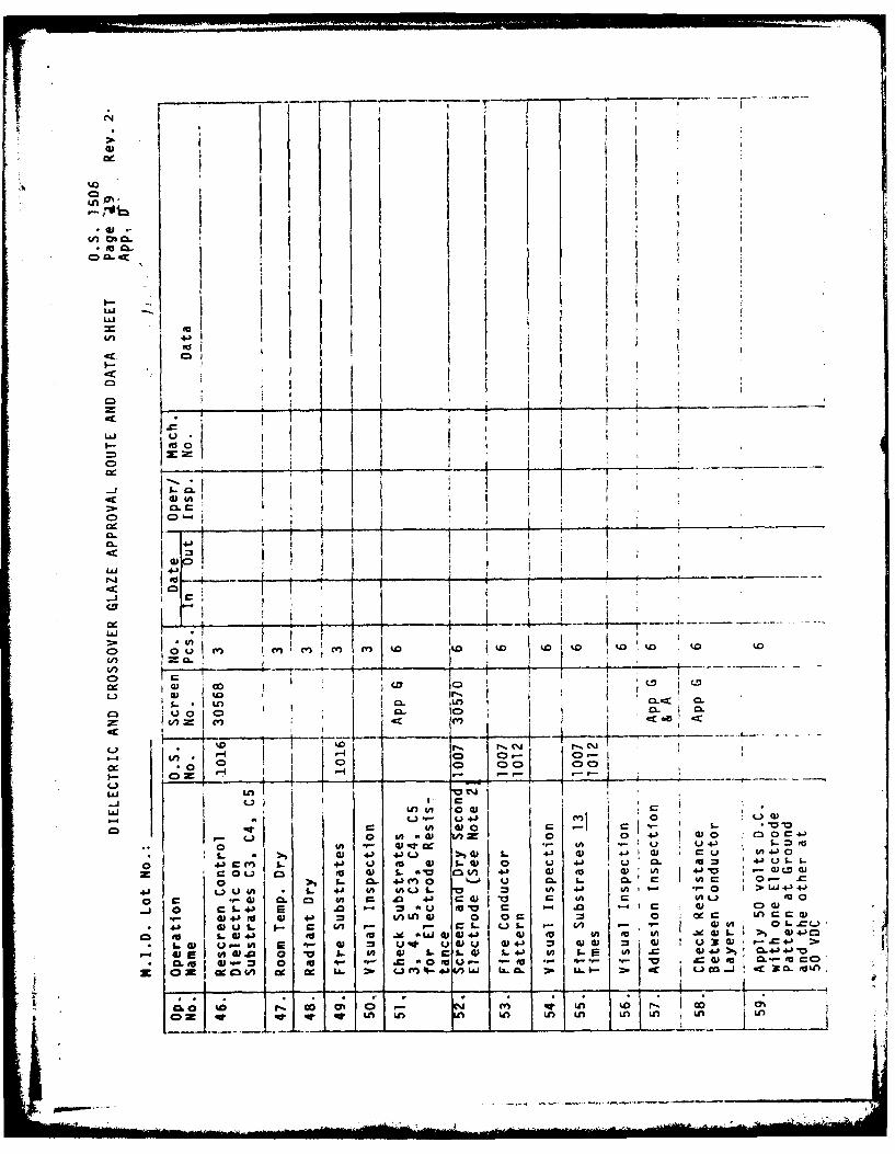
1 I
LA 4
cmIqj I
cri
01L c
91.. 41i- -
C3I rU
>I I
4.) cu tn LC) Iri
__ __ C)..,...I....................~... .r---(n 0 K0 0 t
-cc ItoD tUr- CM K-------
C-) oI ,I_ I IC3 WI4) 0 0 c 0- I
C> o 41 4 a -W 1 4JU 0)P L. 4 )W ru 4 .
I..41 04-1) ' 6 - C c W c 0
c - W C3 n a 4J c0 uoC~ L-4) v w0) C 04)O
41 to4. w 41 V) w .a 0 0 W c I.'U
W w - u v V ~ V )43 0 D W 4) >
4# 40 Ic v' 4. . 44 V)L G c $-w L 4) 0 0 W 41>- 04- 4 -
zU Ci U, (A cr ce L. :- j * L LA CL :0 LA I.- ]ca C
-~ ~~ - - A- t- I _ _ - -. U '- ~ ~ e ~ -*~~a 0'E C
cz 2=C "t qw "r W& uLu LLO, -n J____ L . -. C- - -
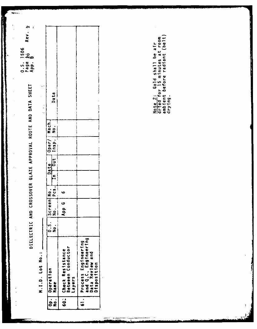
I 5-41-~~5 .0 C .
#A 0 0
00
410) 4-04-) o
~~4 .0 .
LtAO
*41 I -4.
~~fl c"0*0 .. 0c
CL.C5
Go,.9
0 nLn 2m 0.-.
CDP 4
cc C;
LAJ ICOC
w
wc c
"-- 4
-JJ099c -
4- 0 A 0 - CO
C 4 ra) u 194 u fuC
6 0-13, 0-4Wmo c0 # .ct o
0 t c c Im wC
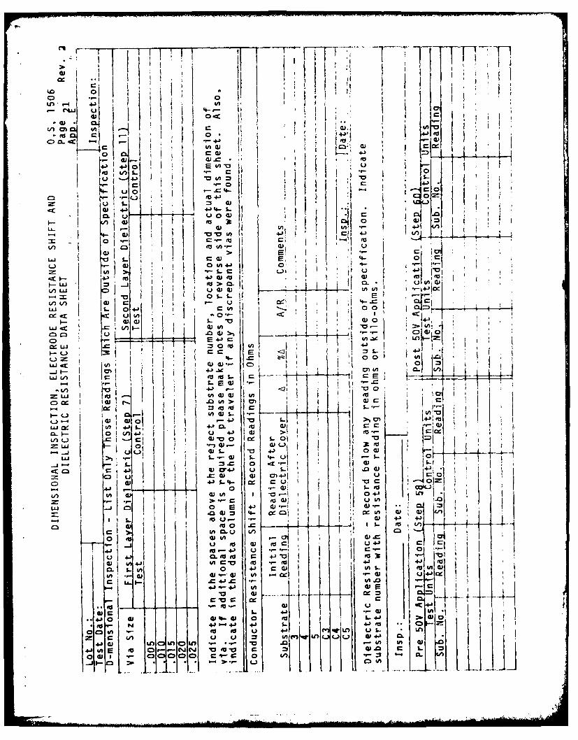
r) r I 43(
w 0
06UaH
4) !I . -
LL4. .) K -I1'
0 4- r_ 0
4- )4 s
06 U W U)0'
V)~~- w oIw~* .0'0I7'I -1 -a)J .0u L. l "
- w 0') W 4LiC
ciJ tio ~ a. (oQ
V)LAJ u w w4I
o S- S...
LI') U)I0) a)) I oI 4
V, 'In9 0 I 0 4
(U (D I -
C)t wiaEU C u~ . 4) 1" I iW L" 3 t 4J4E
0l C.) CLG) 0 I u .EU4J -I.C a-- V
LLI- V) toE
I 0~~~~-0 0 EUj L->oi .. U E U 4'(UL r_
Z: cc r,' .0 I ) n .A04. .
F-.-~ U. b4A *9 a) I-
001~- 0 0 ) 4- 'a 40 0 W- II-
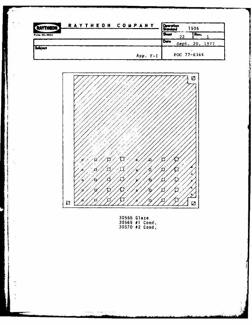
I Sept. 20, 1977
App. F-I POC 77-6344
30568Glaz
306 #1Cod
307/2Cn,
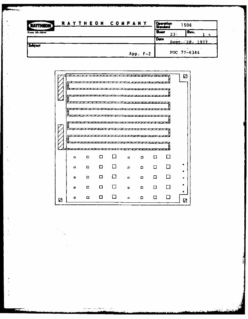
Dwe
App. F-2 POC 77 6344
13 1 0 13 i 0
a 03 0 5 30
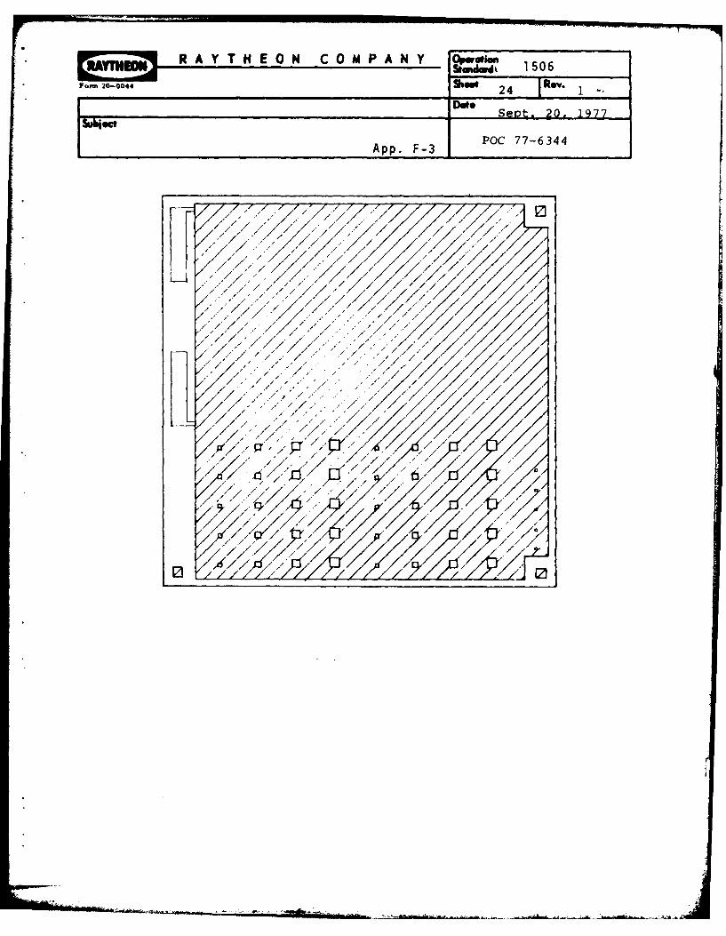
Foram 20-0044 Show 2 4 R. 1I-
App. F-3 POC 77-6344
/1
/ 4' /7 ~o/
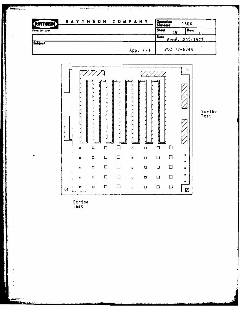
Ponm 20-00 4So
App. F-4 POC 77-644"
0 o 3 0 LI 0 o 0 IoU
1 0 0 0
0 0 0i 0 i o La 0 0 0]a 0 l L
0 0 0l 0l 0I a 0 0 0
Scr01 0ScebTest0 0 Ts
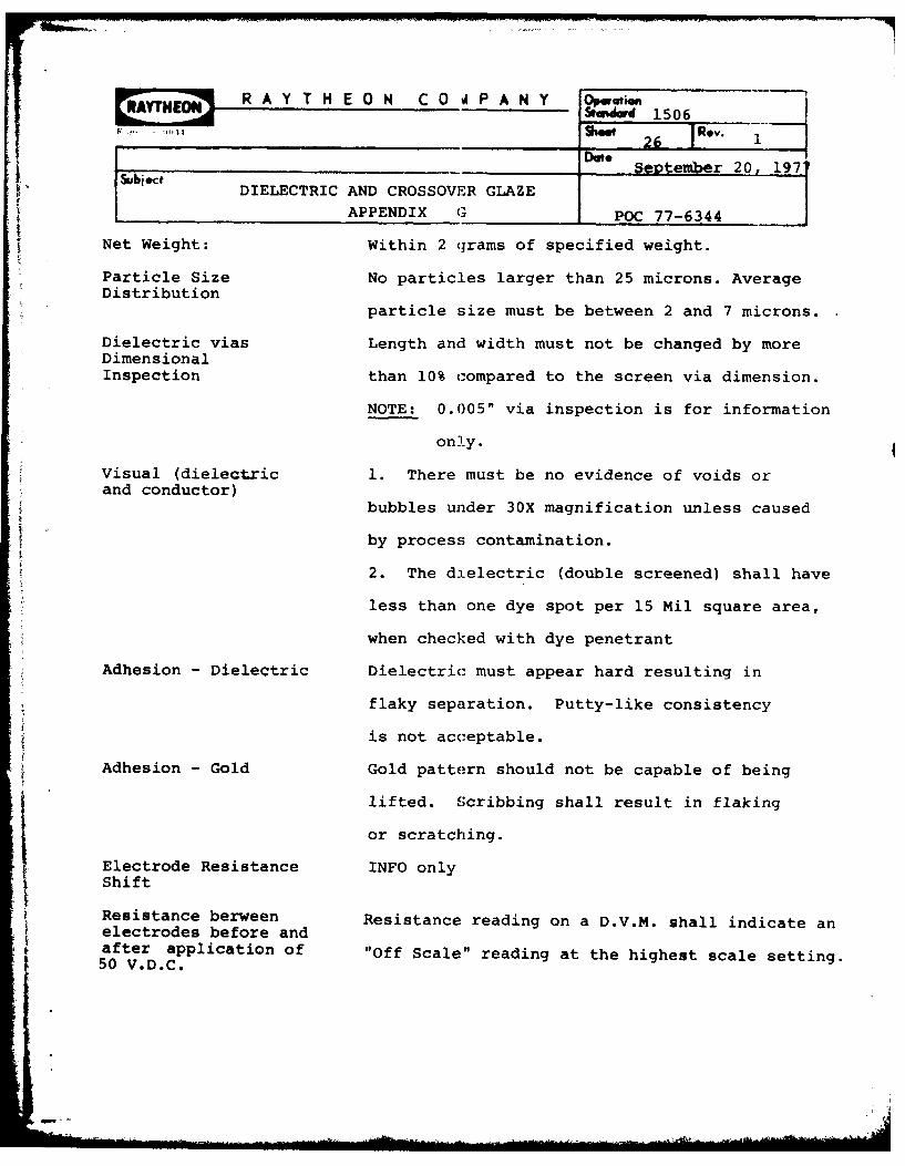
R A Y T H E O N C 0 P A N Y Op,.rUod,,,d 15 0 6; .. . .. , Sho ot 2 6 . 1 *v.
Do*September-20, 17swbi~t DIELECTRIC AND CROSSOVER GLAZE
APPENDIX G POC 77-6344
Net Weight: Within 2 grams of specified weight.
Particle Size No particles larger than 25 microns. AverageDistribution
particle size must be between 2 and 7 microns.
Dielectric vias Length and width must not be changed by moreDimensionalInspection than 10% compared to the screen via dimension.
NOTE: 0.005" via inspection is for information
only.
Visual (dielectric 1. There must be no evidence of voids orand conductor)
bubbles under 30X magnification unless caused
by process contamination.
2. The dielectric (double screened) shall have
less than one dye spot per 15 Mil square area,
when checked with dye penetrant
Adhesion - Dielectric Dielectric must appear hard resulting in
flaky separation. Putty-like consistency
is not acceptable.
Adhesion -Gold Gold pattern should not be capable of being
lifted. Scribbing shall result in flaking
or scratching.
Electrode Resistance INFO onlyShift
Resistance between Resistance reading on a D.V.M. shall indicate anelectrodes before andafter application of "Off Scale" reading at the highest scale setting.50 V.D.C.
oDx(n -4 -I
*a)G)
a4-
0 -, M I-
a) I1 0 I
044- U).- z~~I>1> 0, 4
0 4J 4J
(aJO (a _ _ _ _ __I_ _ _
0% 41 4 4 11 0 ): a)Cf0
04m 0 *z04
000 CO4J4- 4JQ
0 0 00 M (
U
00 10 0 0 o .
-- r
H0 U UiQ r- CN 0 , 0E- 2D 0 0 -4 04 04 '- - I
0-)0 0 *0 Q 0 04~ 04 0 ;:w PZ4 z0Z -z -41 ~-4 I- <
H 0$4 2 0 a) W4Ja) a~~() U) 0 .~ 0u c.0 4.3 4Cf 0 0 e 0 4 34 -4r)
0 00. . 4 ( 41~ a) 4J j C :,020 (D .41 4 u 0 r1. ) 413 43 () CL
V 00 6M 413 10 3 TA H9 M) ~ u c U 'U9~. U) z z 4 U)n r.0J' r 0- () 0"- 0 0 -
-~0 0 . 00 H 00 E- $4 U S- El 0)0 4.34. 4q 2 0 4-1 4.1 -J3 0 -4.,14. C/0 04Jr u - u c r-u E n -4
0 .4 0) a) ljM 1 :3 a) (D I a) (az~~~ ~ to Ix~ I'' a ul ) -4'~ a)r00 a0 0 a. -4 (a0 0 .1 H4 ~0 u~ H u .4 00-.--41 t V 0 Nz 020 U > 00 L 0U)2M U 0O ~ ~~~I
M )00r. __ __-4_IX __ 4_ >_ )
0 z 4 ~ - -r- 0
AD-AO86 344 RAYTHEON CO QUINCY MASS INDUSTRIAL COMPONENTS OPERATION F/6 9/1MANUFACTURING METHODS AND TECHNOLOGY ENGINEERING (MM AND TE) PR--ETCIU)APR 80RI M ZILBERSTEIN OAA007-76-C AIlq
UNCLASSIFIED DELET-TR-76-8119-F VOL 2 NL
MEO
132
I.3 6
IIIJIL25 1 16
MICROCOPY RI SOLUION I ST CHART
HAON I W I I 0 1 ,N , W, , ,,, ,, A
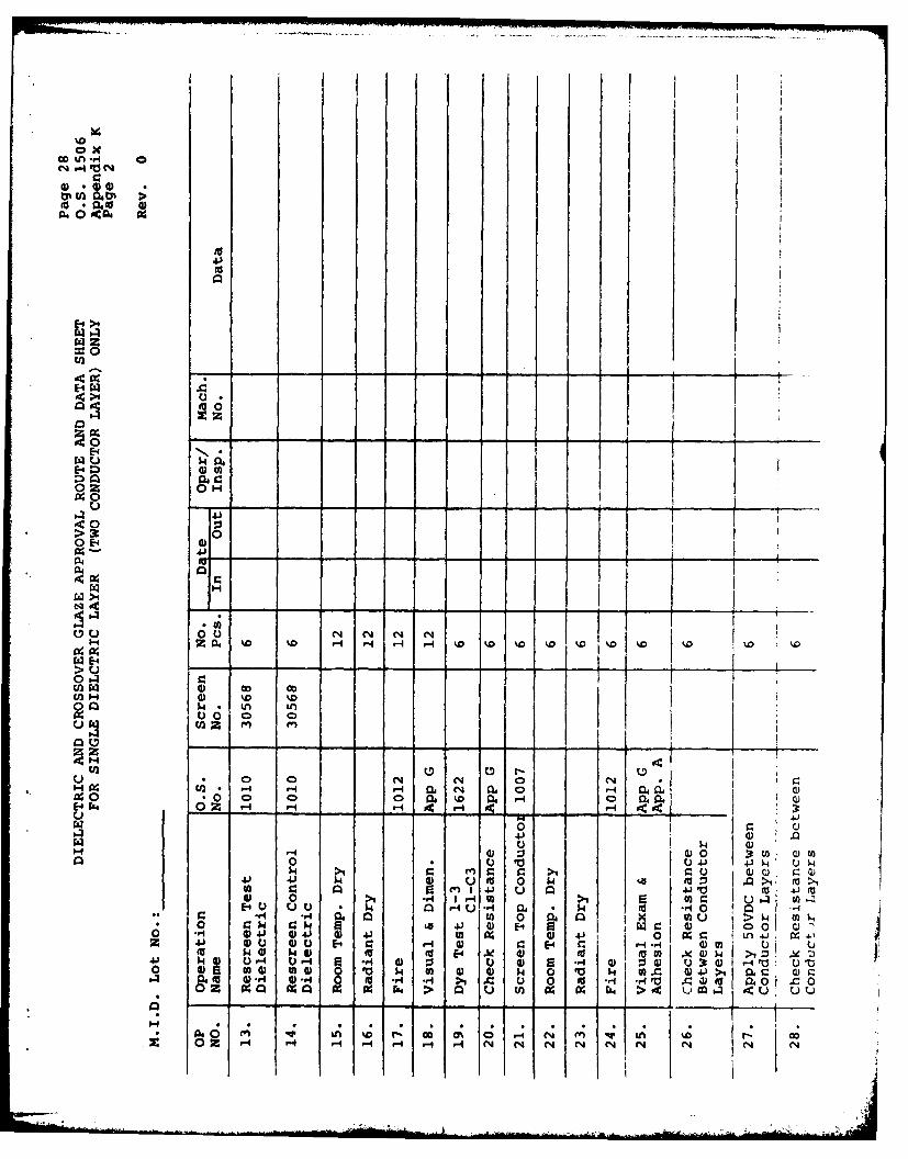
~000U)c -AC*4 r-4 to 4
4) 4)040N
= 0
0.
00
1'1
00 0 N C~
> u.
04 l
0 04 0
204~~ ~O 'O cI cI . - 0 '0 0 N 0HC14 o
000 0
E-4 P 0 Z6
u m -w--- 440I
*~ 4)-)
0 44 0)?A 9 0(nI 4J U 0W 410 (aCf4) 0 * 0z .(n 40) 4~4
E-0 i U t I H 0 Im -M) 4) t40 o 0 i W u .> .$41 W
0 f 9' ;* 0 p w~l4 0 a) 0t 4J0.H 0 *.1 w s 0w 9 tn-. z*04 4J 1 w c-U4 O * 140PI 0 izc 4JI 04 0 0 04E" C: r-4U i>E-4to 04 -$~4 to1 ~ ~ ~ 0J
00 0 0 to w w)0 0 . 0 0 0)W 0 4)> 04~ 0)0. I 3A' 0> 0D (a *c. 0 Cc4 0
* 0e u) Wn Ix) '.0 >- 4 Ot0-I m(44
z 02 -I -4 - 4 -4 -I r-4 ('4 N %4'C44 N .
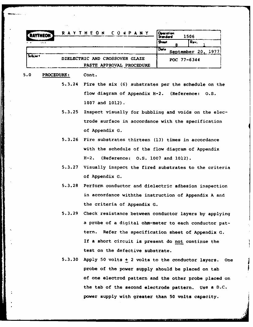
Rj ; AECRAYTHPANY OONrCOiofiNStdad 1506
Date September 20,_ 1977
DIELECTRIC AND CROSSOVER GLAZE POC 77-6344
PASTE APPROVAL PROCEDURE .....___
5.0 PROCEDURE: Cont.
5.3.24 Fire the six (6) substrates per the schedule on the
flow diagram of Appendix H-2. (Reference: O.S.
1007 and 1012).
5.3.25 Inspect visually for bubbling and voids on the elec-
trode surface in accordance with the specification
of Appendix G.
5.3.26 Fire substrates thirteen (13) times in accordance
with the schedule of the flow diagram of Appendix
H-2. (Reference: O.S. 1007 and 1012).
5.3.27 Visually inspect the fired substrates to the criteria
of Appendix G.
5.3.28 Perform conductor and dielectric adhesion inspection
in accordance withthe instruction of Appendix A and
the criteria of Appendix G.
5.3.29 Check resistance between conductor layers by applying
a probe of a digital ohm-meter to each conductor pat-
tern. Refer the specification sheet of Appendix G.
If a short circuit is present do not continue the
test on the defective substrate.
5.3.30 Apply 50 volts + 2 volts to the conductor layers. One
probe of the power supply should be placed on tab
of one electrod pattern and the other probe placed on
the tab of the second electrode pattern. Use a D.C.
power supply with greater than 50 volts capacity.
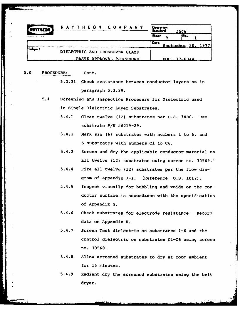
R A Y T H E 0 N C 0 0 P A N Y Oped 10rRAYTHW 150 6, .... ... a .Sho 9 -- R Oev.Re.1
_ _ DateSeptember 2._1227DIELECTRIC AND CROSSOVER GLAZE
. ......_PASTE APPROVAL HROCEDURE POr 77-6144
5.0 PROCEDURE: Cont.
5.3.31 Check resistance between conductor layers as in
paragraph 5.3.29.
5.4 Screening and Inspection Procedure for Dielectric used
in Single Dielectric Layer Substrates.
5.4.1 Clean twelve (12) substrates per O.S. 1000. Use
substrate P/N 26219-29.
5.4.2 Mark six (6) substrates with numbers 1 to 6, and
6 substrates with numbers Cl to C6.
5.4.3 Screen and dry the applicable conductor material on
all twelve (12) substrates using screen no. 30569.'
5.4.4 Fire all twelve (12) substrates per the flow dia-
gram of Appendix J-1. (Reference O.S. 1012).
5.4.5 Inspect visually for bubbling and voids on the con-
ductor surface in accordance with the specification
of Appendix G.
5.4.6 Check substrates for electrode resistance. Record
data on Appendix K.
5.4.7 Screen Test dielectric on substrates 1-6 and the
control dielectric on substrates Cl-C6 using screen
no. 30568.
5.4.8 Allow screened substrates to dry at room ambient
for 15 minutes.
5.4.9 Radiant dry the screened substrates using the belt
dryer.
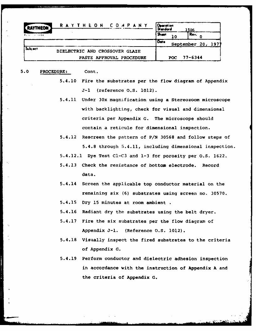
N EO' R A Y T H E 0 N C 0 4 P A N Y Oi:Me, i 0 10Shwdd 1506
Re.0
Do_ September 20, 1977Subg~t DIELECTRIC AND CROSSOVER GLAZE
PASTE APPROVAL PROCEDURE POC 77-6344
5.0 PROCEDURE: Cont.
5.4.10 Fire the substrates per the flow diagram of Appendix
J-1 (reference O.S. 1012).
5.4.11 Under 30x magnification using a Stereozoom microscope
with backlighting, check for visual and dimensional
criteria per Appendix G. The microscope should
contain a reticule for dimensional inspection.
5.4.12 Rescreen the pattern of P/N 30568 and follow steps of
5.4.8 through 5.4.11, including dimensional inspection.
5.4.12.1 Dye Test Cl-C3 and 1-3 for porosity per O.S. 1622.
5.4.13 Check the resistance of bottom electrode. Record
data.
5.4.14 Screen the applicable top conductor material on the
remaining six (6) substrates using screen no. 30570.
5.4.15 Dry 15 minutes at room ambient .
5.4.16 Radiant dry the substrates using the belt dryer.
5.4.17 Fire the six substrates per the flow diagram of
Appendix J-1. (Reference O.S. 1012).
5.4.18 Visually inspect the fired substrates to the criteria
of Appendix G.
5.4.19 Perform conductor and dielectric adhesion inspection
in accordance with the instruction of Appendix A and
the criteria of Appendix G.
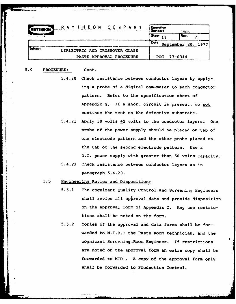
R A Y TH E O N C 0 4 P A N Y O nerae.RtWdrd ISOSho 1. .Rev. -
Dc*a September 20, 1977
sbg DIELECTRIC AND CROSSOVER GLAZE
PASTE APPROVAL PROCEDURE POC 77-6344
5.0 PROCEDURE: Cont.
5.4.20 Check resistance between conductor layers by apply-
ing a probe of a digital ohm-meter to each conductor
pattern. Refer to the specification sheet of
Appendix G. If a short circuit is present, do not
continue the test on the defective substrate.
5.4.21 Apply 50 volts +2 volts to the conductor layers. One
probe of the power supply should be placed on tab of
one electrode pattern and the other probe placed on
the tab of the second electrode pattern. Use a
D.C. power supply with greater than 50 volts capacity.
5.4.22 Check resistance between conductor layers as in
paragraph 5.4.20.
5.5 Engineering Review and Disposition:
5.5.1 The cognizant Quality Control and Screening Engineers
shall review a].l apbroval data and provide disposition
on the approval form of Appendix C. Any use restric-
tions shall be noted on the form.
5.5.2 Copies of the approval and data forms shall be for-
warded to M.I.D.; the Paste Room technician, and the
cognizant Screening.Room Engineer. If restrictions
are noted on the approval form an extra copy shall be
forwarded to MID . A copy of the approval form only
shall be forwarded to Production Control.
RAYT H E 0 N C 0 aiP A N Y Oiw,,ion*An N CA1dd . 1506
.. Show,, 12 Re,,. I
tD4 September 20, 197
15"E~c DIELECTRIC AND CROSSOVER GLAZE
PASTE APPROFAL PROCEDURE POC 77-6344
5.0 PROCEDURE: Cont.
5.5.3 Upon receipt of an approved form, the MID inspector
shall label the subject paste jar with either an
accept or reject notation. If a restriction is noted
on the approval form, a notation of the jar shall be
placed with the words "Restricted - Use". A copy
of the approval form shall also be provided by MID
and placed with the subject jar, if the jar has a
use restriction.
5.5.4 Rejected jars shall be placed in a special "Reject
Area" until appropriate disposition os the rejected
jar is made.
R A Y T H E O N C O M P A N Y o-t1= 150...... .,wd, 1506 - 2i
W E. '4~1 Rev.1
Do" Sept. 20, 1977ADHESION TEST PROCEDURE APPENDIX A POC 77-6344
1.0 EQUIPMENT:
Phono-Point Diamond Tip (750 Angle) and. Microscope with lOX to 30X
magnification.
2.0 PROCEDURE:
Use the diamond tool and microscope to perform the following test.
2.1 Metallization (Conductor) to Dielectric:
With the diamond tip scribe one electrode test pad with moderate
force at approximately a 450 angle from the surface of the substrate
and in a direction away from the tester. When testing the "second
electrode pattern" a separate gold conductor pattern has been provided
at the upper right of the substrate for this purpose. See Appendix F-4
pictorial.
2.2 Adhesion of Dielectric to Substrate and Dielectric Hardness:
Test as in 2.1 above except that the area to be scribed will be any
corner of the dielectric at the lower portion of the substrate. See
Appendix F pictorials.
3.0 OBSERVATION:
Record all observations in the Data Column of the lot traveler. Use
descriptive words indicating adhesion of dielectric and conductor materials.
Such words as flaking and peeling are appropriate. If the dielectric cuts
like "putty" make such a notation. The amount of hand pressure required to
scribe should be noted, such as light force, moderate force, etc. Also the
layer at which separation takes place should be noted.
4.0 Refer Appendix G for specifications.
E ol~r H O LOMPAN ke8d 1506_ _......._ _ _ _Show 14 R". 1
Dc-. Sept. 20, 1977iCf PASTE RECEIVAL AND RECORD FILE (MID FORM) POC 77-6344
APPENDIX B J
Date Received:
Date Approved/Rejected:
Paste Name:Part No.:
Vendor:MID Lot No.:
P.O. No.-.
Vendor Lot No.:
Vendor P/N:
Weight Per Jar From Label:
Other Label Data:
Accepted: Rejected:
Restrictions - List Below: Reason For Rejection And Disposition:
____________ _ ____ ___ Sept. 20, 1977
Sabject
ENGINEERING APPROVAL VERIFICATION POC 77-6344________________ APPENDIX C___________
Paste Type No.: _________
MID Lot No.:___________
Jar No.:______________
Vendor:_______________
Vendor Lot No.:___________
P.O. No.:_____________
Weight:_______________
Date Rec'd:____________
Approval Completed:_________
Data Review: Record below any test results not meeting specification.
Di spositi on:
Accept:__________ Reject: Complete IMR If Rejected
Use Restriction:
Quality Control Engineering:___________ Date:_________I Paste Engineer:__________________ Date:_________
RA 1.R A Y PL.. .PAN Y Opwaoe.... . .... . ..... .. ... .. .. ... .. . siw od w 1 6 8 5
.. .... WO- 1. Rev. 0o
Feb. 21, 1978
tPOC 78-6061PASSIVE LASER TRIM/ LOAD & UNLOAD
1.0 PURPOSE:
To laser trim fired resistors to specified values by reducingthe effective area of the resistor.
2.0 SAFETY:
Hands will remain outside the work area (under hood) whiletrimming.
3.0 EQUIPMENT:
ESI, model 44, laser trim system with proper substrate nest.Passive trim program.
4.0 PRODUCT REQUIREMENT:
See applicable OS # for screening, laser trimmable, substrates.
5.0 PROCESS REQUIREMENT:
A. Set Up
1. Technician, or engineer, will access passive trim program.
2. Adjust, aliqn and position substrate for proper probe contact.
3. The actual trim path will be checked and corrected as neccessary.
4. Verify the laser measurement system with an off line bridge.
6.0 PRODUCTION RUN:
A. Trim
1. Technician will call laser system into run mode.
2. Position substrate- using required bank points, on handler.
3. Depress foot peddle, position subtrate in work area, andrelease foot peddle.
1 2
0 !0. I I I I .
~~~R A Y T H E 0 N C 0 M P A N Y " 18COMPA Y .= 1685
.. ' 2 Re'v. 0
0* .Feb. 21, 1978i ' POC 78-6061
PASSIVE LASER TRIM/LOAD & UNLOAD
6.0 PRODUCTIVE RUN: Cont.
4. Press the proceed button on the console.
5. While substrate is being trimmed load the next substrate.
6. An accept, and/or reject light will inform the operatorwhether or not substrate is acceptable.
7. After trim completion, depress peddle and slide handlerto position next substrate. Release peddle and removetrimmed substrate.
8. Press the procede button.
9. Repeat steps 2 through 9 until 5 pieces have been trimmed.
10. Give the first 5 pieces to Q.C., for visual and posttrim, in process inspection.
11. Upon Q.C. acceptance, switch man/auto switch to auto,and proceed with steps 2 through 9. While in auto, theprocede button does not have to be used.
7.0 SALVAGE:
All rejects will be inspected by laser personel and salvaged,if possible.
=" August 16, 1978TCVCXO CRYSTAL CONTROL POC 78-6441
1.0 This instruction provides details for the control of crystals used in theTCVCXO module. (ECOM Program) Note: Crystals and crystal curves for thisprocram are supplied by the government. Universal, Raytheon, I.C.O. proceduresare applicable to this program except as modified herein.
2.0 RECEIVING:
2.1 The receiving department shall apply an identification lot number to theshipping container. Copies of the receiving report shall be distributedto the DCAS representative and the Government Property Administrator.After normal administrative receiving procedures have been completed theproduct shall be delivered to the receiving inspection department (MID).
2.2 The receiving inspection department (MID) shall perform all normal ad-ministrative functions and provide inspection in accordance with theapplicable receiving inspection instruction (detail sheet).
2.3 MID personnel shall apply the lot number and "Letter Designation" (Seepara. 2.4) to all graph sheets and other pertinent received documentsand MID data sheets. After the markings have been affixed a copy ofeach received document shall be made and forwarded with the product.The original documents shall be maintained on file in MID.
2.4 Letter Designation - Each lot number shall have a corresponding letterdesignation. A chart shall be maintained in MID to show the correspondingletter designation for each lot. The letter designation shall comencewith A. The second twenty six lots shall be labeled AA, AB, AC, etc.the third group of twenty six lots shall be labeled BA, BB, BC, etc.
2.5 Labeling of Crystals - The lot letter designation shall be applied toeach crystal using pencil.
Ceramic packaged crystals - apply directly to ceramicOval crystal can package - apply to gummed label already on canTO 5 package - apply to gummed label and stick to can. Use onlylabels which require wetti of adhesive.
2.6 Crystal identification log - MID personnel shall provide the crystalidentification log form. (App. A) They shall fill out the MID sectionof this form and forward the form to stores with the accepted product.The column labeled "Turning Pt.,&.Hz" requires calculated data derivedfrom the curves supplied. In addition the trimmed values of R47 andR48 of the TCFG module shall be determined from the turning point.These values shall be recorded in the appropriate columns. A table
f I will h and R_
R A Y T H E O N C OM P A NY 1721SAugust 16, 1978
TCVCXO CRYSTAL CONTROL POC 78-6441
2.0 RECEIVING: CONT.
2.7 Rejected material - A material review form shall be filled out and therequired signature obtained. In addition the DCAS representative shallbe notified by the cognizant quality control engineer on a verbal basis.A copy of any resulting Material Review Disposition Report shall be for-warded to the Government Property Administrator.
2.8 Delivery to stores - The accepted crystals, the applicable graphs (curves)and the crystal identification log shall be forwarded to the stockroom.
3.0 STOCKROOM:
3.1 Stores personnel shall store the crystals in an area (shelf) designated"Government Furnished Material". The accompanying curves shall bestored with the product. The crystal identification log sheet shall beplaced in a permanent "Crystal Log" notebook,
3.2 VCXO Kit Assembly - Stores personnel shall provide VCXO Kits for produc-tion control requirements. The kits shall be organized into lots andidentified with the standard six digit hyphenated lot number. Stockroom personnel shall provide three documents for each kit. These are:
3.2.1 The standard lot traveler
3.2.2 The crystal - VXCO Identification Log (see para. 3.4)
3.2.3 Stores issue sheet which will provide traceability for all semi-conductor, capacitor, and substrate lots,
NOTE: The crystal is part of the VCXO Kit.
3.3 TCFG Kit Assembly - Stores personnel shall provide TCFG Kits for produc-tion assembly in accordance with production control requirements. Thekits shall be organized into lots and identified with the standard sixdigit hyphenated lot number. Stock room personnel shall provide threedocuments.
3.3.1 The standard lot traveler
3.3.2 The crystal - TCFG Identification log (see para. 3.5)
3.3.3 Stores issue sheet which will provide traceability for all semi-conductors, capacitors, and substrate lots,
A THE C0M N Yi 1721
13 June 1978
TCVCXO CRYSTAL CONTROL POC 78-6321
3.0 STOCKROOM: CONT.
3.4 The Crystal - VCXO Identification Log (See App. C)
3.4.1 Stockroom personnel shall initiate the crystal - VCXO log andmaintain a copy in stores. An equal number of crystals shallbe assigned to the lot. The Crystals letter lot designation andserial nos. shall be recorded in their respective columns.
3.4.2 The VCXO serial number range shall be assigned to each VCXO lot.The number shall consist of a hyphenated five (5) digit code.The first three (3) digits shall be the last three (3) digits ofthe lot number. A hyphen shall follow. The number shall endwith a two (2) digit sequential number. The serial number rangeshall be recorded in the appropriate spaces of the Crystal-VCXOidentification log. A copy of the Crystal-VCXO log shall be atta-ched to the VCXO lot traveler.
3.5 The Crystal - TCFG Identification log (See app. D.)
3.5.1 Stockroom personnel shall initaite the crystal TCFG log and main-tain a copy in stores. A VCXO lot shall be astigned to theTCFG lot. The R47 and R48 values associated with each crystalshall be recorded on the TCFG log. These values may be obtainedfrom the crystal identification log.
3.5.2 TCFG serial numbers shall be assigned to each TCFG lot. Thenumber shall consist of a hyphenated five (5) digit code. Thefirst three (3) digits shall be the last three (3) digits of thelot Aumber. A hyphen shall follow. The number shall end witha 2 digit sequential number. These range of serial numbers shallbe recorded in the appropriate spaces of the Crystal-TCFG identi-fication log. A copy of the Crystal-TCFG log shall be attachedto the TCFG lot traveler.
3.6 Completed VCXO and TCFG lots shall be returned to stores. Productionshall form kits using the above modules for marriage of the VCXO andTCFG modules. The Crystal identification log should be used to match theappropriate VCXO and TCFG lots.
3.7 Defective modules with good crystals - Good crystals removed from defec-tive modules shall be returned to stores. Stores personnel shall reassignthe crystal to other VCXO and TCFG units. PrOper notation of this trans-fer shall be made on all log sheets. Line numbers on the crystal identi-fication log are provided so that reference may be made by line numberto indicate the transfer of the crystal.
3.8 Defective crystals shall be returned to stores and a new crystal assignedto the applicable VCXO and TCFG modules. All logs should reflect thisnew assignment. The defective crystal shall be transferred to MID whereappropriate administrative action shall take place.
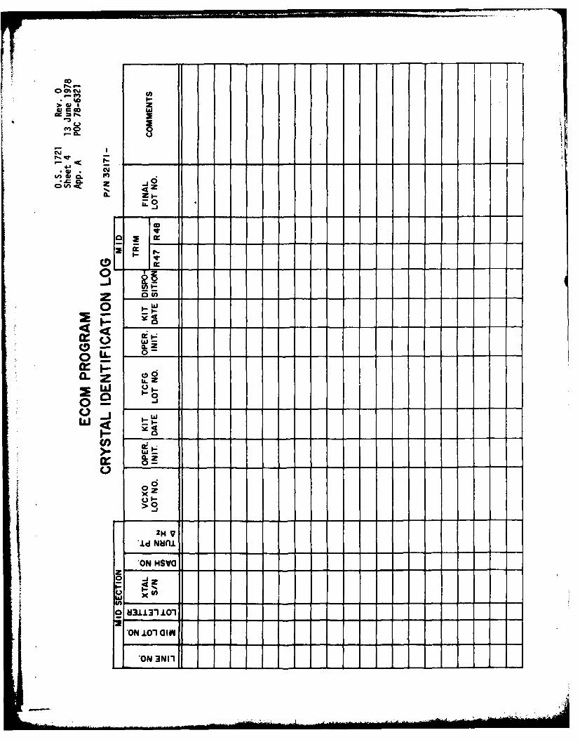
cO C.
w cooIC.AI
41~
.4 . CY
.. c CL
cl- 44OI2z_
0.0
[LI- T
0-0 LL.
0
ozx0 '->0q
0
X
H31A±±3101
ON 101 OIN
-0N 3N11I
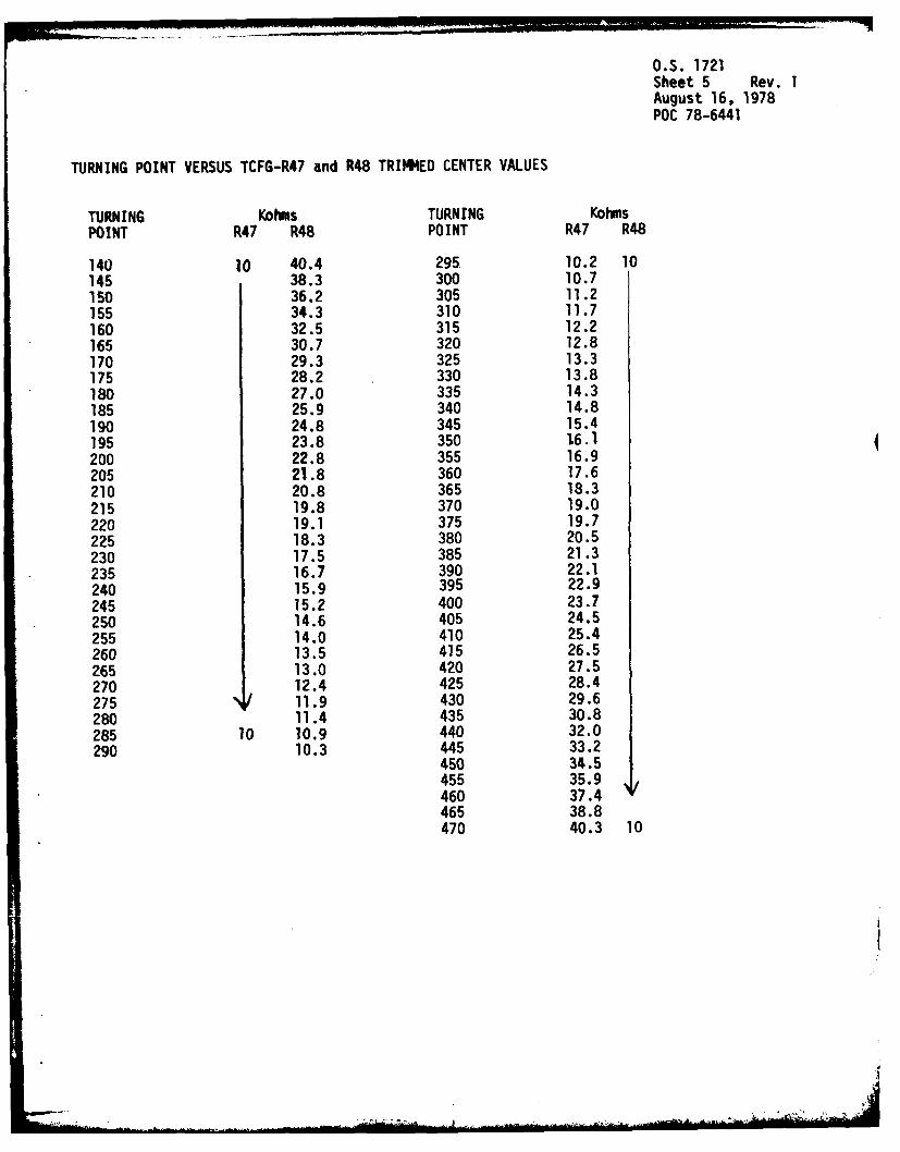
O.S. 1721Sheet 5 Rev. 1August 16, 1978POC 78-6441
TURNING POINT VERSUS TCFG-R47 and R48 TRIMMED CENTER VALUES
TURNING Kohms TURNING KohmsPOINT R47 R48 POINT R47 R48
140 10 40.4 295 10.2 10145 38.3 300 10.7150 36.2 305 11.2155 34.3 310 11.7160 32.5 315 12.2165 30.7 320 12.8170 29.3 325 13.3175 28.2 330 13.8180 27.0 335 14.3185 25.9 340 14.8190 24.8 345 15.4195 23.8 350 16.1200 22.8 355 16.9205 21.8 360 17.6210 20.8 365 18.3215 19.8 370 19.0220 19.1 375 19.7225 18.3 380 20.5230 17.5 385 21.3235 16.7 390 22.1240 15.9 395 22.9
245 15.2 400 23.7250 14.6 405 24.5255 14.0 410 25.4260 13.5 415 26.5265 13.0 420 27.5270 12.4 425 28.4275 11.9 430 29.6280 11.4 435 30.8285 10 10.9 440 32.0290 10.3 445 33.2
450 34.5455 35.9460 37.4465 38.8470 40.3 10
I *~- - .~'
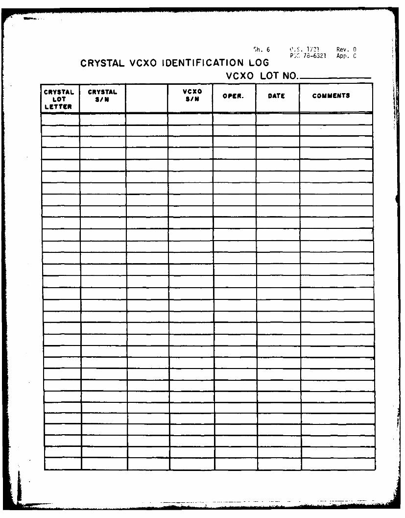
")h. 6 C li.172 Rev. 0P'-" 78-6321 App. C
CRYSTAL VCXO IDENTIFICATION LOGVCXO LOT NO.
CRYTA CRSTAL VCX OPEN. DATE COMMENTSLETTER
Sh. 7 O.S. 1721 Rev. 0
CRYSTAL TCFG IDENTIFICATION LOG PC7-31Ap_____ ___ __ _ ____ TCFG LOT NO. _ _ _ _ _ _
CRYSTAL CRYSTAL TRIM TCF6 OPER. DATE COMMENTSLOT S/N S/N
LETTER Rt47 R11S_______~~~ ~ it___ _ K KA __ _ _ _ __ _ _ _ __ _ _ _ _ _ _ _ _ _ _ _
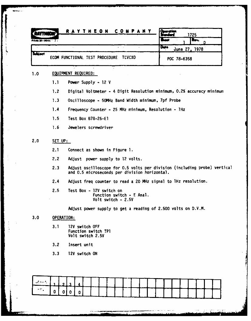
• / RA Y T H E 0 Hl C 0 M P A N Y 12
1725
_June 27, 1978
ECOM FUNCTIONAL TEST PROCEDURE TCVCXO POC 78-6358
1.0 EQUIPMENT REQUIRED:
1.1 Power Supply - 12 V
1.2 Digital Voltmeter - 4 Digit Resolution minimum, 0.2% accuracy minimum
1.3 Oscilloscope - 50MHz Band Width minimum, 7pf Probe
1.4 Frequency Counter - 25 MHz minimum, Resolution - IHz
1.5 Test Box B78-25-El
1.6 Jewelers screwdriver
2.0 SET UP:
2.1 Connect as shown in Figure 1.
2.2 Adjust power supply to 12 volts.
2.3 Adjust oscilloscope for 0.5 volts per division (including probe) verticaland 0.5 microseconds per division horizontal.
2.4 Adjust freq counter to read a 20 MHz signal to 1Hz resolution.
2.5 Test Box - 12V switch onFunction switch - E Anal.Volt switch - 2.5V
Adjust power supply to get a reading of 2.500 volts on D.V.M.
3.0 OPERATION:
3.1 12V switch OFFFunction switch TPIVolt switch 2.5V
3.2 Insert unit
3.3 12V switch ON
- - -- -m4
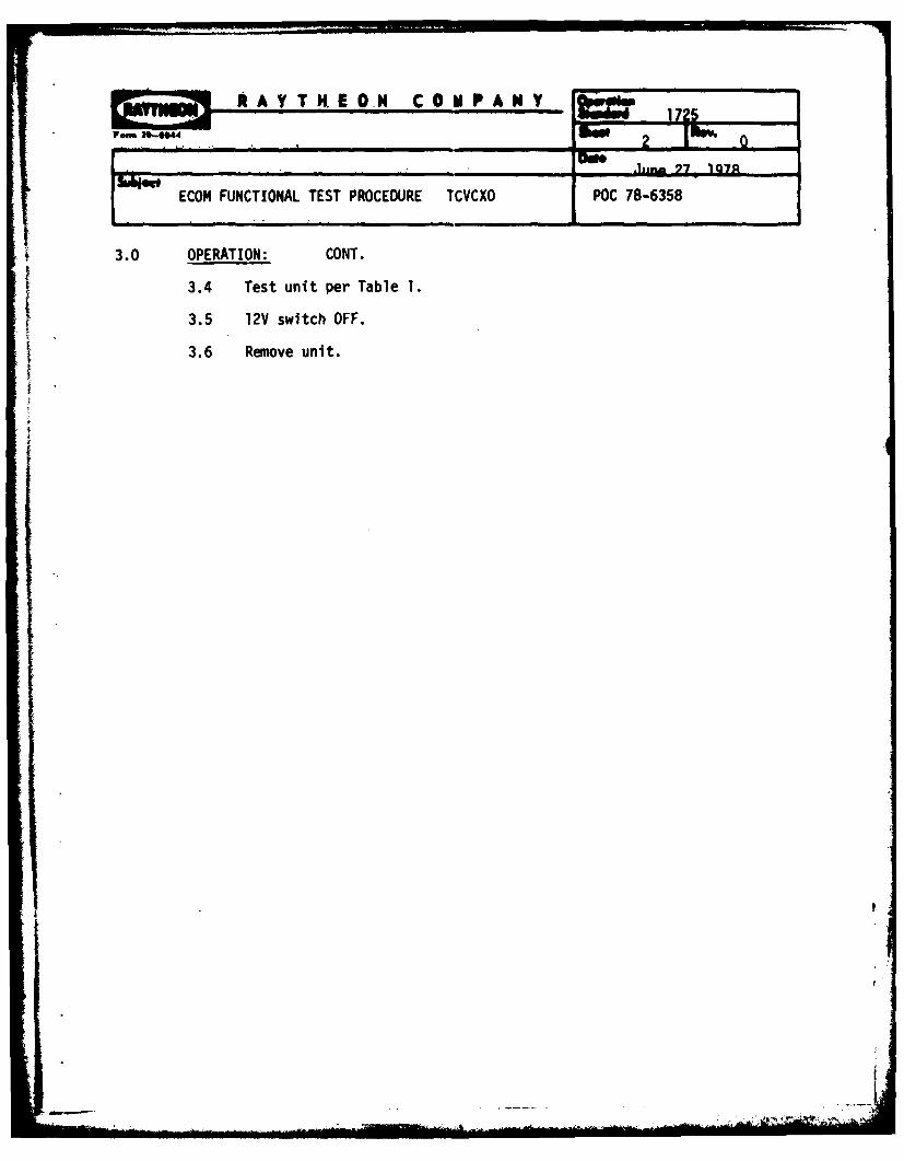
3.0 OP RAN: CONMP N
ILW 17J
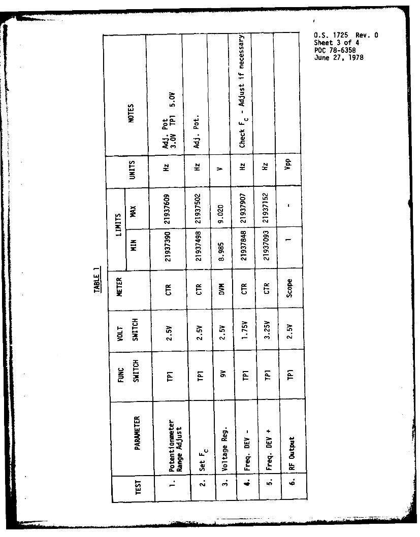
-- 0.S. 1725 Rev. 0Sheet 3 of 4
4A POC 78-6358u June 27, 1978
C
4~-
41,
Lnn
I--
240C 4.' C U"00 IL..O
a. a.P l-
ON C NON NCh
oD 0o 0o cIt) ONi q "
mu u o ~ c'.J Cv
0% 03N
Zo -l . O
Cu Cu On r- Cui
i-i (.. 0- C .. L)
U. V- F.-.~. U
0 2j LA
In~c 4JC u ,- () C
W 0. L. o . . A-LhL V) LA -- L. -
C. W
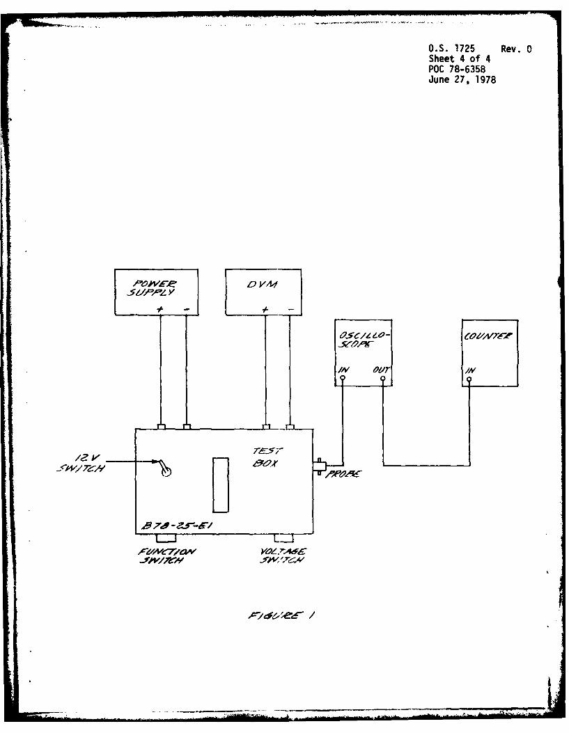
0.S. 1725 Rev. 0Sheet 4 of 4POC 78-6358June 27, 1978
//,'L YD Y
* - /
O5C/Z / O- CEO6'/-/i'7-
ii L1J-/ Par
.Ar I ,* VO .4A~
-W/VI 7 # -ell t~t
,Li '.E
Fem -0044 . . ... o 1 iftW " 0
J -Dowe Oct. 19, 1978
ECOM-TCFG PASSIVE TRIM SET-IP POC 78-6572
1.0 REQUIRED MATERIAL:
1.1 Model 44, ESi Laser Trim System
1.2 TCFG Substrate Nests (2)
1.3 Software Programs:
A. TK2B. Pass 1. TCFC. Pass 2. TCFD. Focus
2.0 SET UP:
2.1 Insure all Quality Inspection Gates have bee. completed beforetrimming substrates.
2.2 Locate mount, and properly position substrate nests on handler.
3.0 LASER FOCUSING:
3.1 Call focus from floppy di:sk into the PDP-11/04 computer. Thisis done in the following manner.
RL__jFocus if on FDN diskRU'JFDI: Focus i. on FDl disk
3.2 Focus will ask for power, speed of cut, length of cut, andoffset. The proper responses will be determined by thetechnician.
3.3 After executing focus, inspect substrate sample.
4.0 FOCUS INSPECTION:
4.1 Look for excessive kerf (laser trimmed area) width of X and Y.
4.2 Excessive substrate penetration ('8 um) should be addressed first.
4.3 After determining power and speed requirements, reiterate focus.
4.4 Inspect for kerf width's X & Y (they should be the same).
1 2 3 1
0 0 0 0
M P AN Y 1748
Iro, 2004 2 1Rv. 0_ _..Deft_ Oct. 19, 1978
ECOM-TCFG PASSIVE TRIM SET-UP POC 78-6572
4.0 FOCUS INSPECTION: Cont.
4.5 Inspect for substrate penetration X and Y. (They should bethe same).
4.6 Once kerf width is 1 to 2 mils, substrate penetration 4 to 8microns, the laser is properly focused. Lock lense in place.
5.0 PROBE CARD ALIGNMENT AND ADJUSTMENT:5.1 This procedure will be repeated twice. TCFG substrates require
two trimming passes.
5.2 Pass 1 requires pass I.TCF software support and TCFG-I probe card.
Pass 2 requires pass 2.TCF software support and TCFG-2 probe card.
Note: Cards and software are not interchangeable.
5.3 Mount probe card adapter and fasten firmly.
5.4 Insure proper handler height before installing fixed probe card.Adjust to maximum height initially.
5.5 Adjust down travel limit, on handler, for minimum down travelinitially.
5.6 Run TK2, get proper software support, and proceed. TK2 willallow joy stick control of table.
5.7 After initial handler adjustments, gently insert probe card intoadapter without bumping probes.
5.8 Firmly adjust slide fails on probe card. Do not tightenat this time.
5.9 Locate substrate on nest and rotate handler into work area.
5.10 Align X, Y, i on substrate holder (nest) until all probes arein approximately the right area.
5.11 Slowly adjust down travel, insuring probes clear all obstructions(corral), to approx. 1/16 of an inch above substrate.
5.12 Re-align substrate nest. and card holder until all probes areproperly located.
5.13 Adjust handler up travel limit for 20 mils minimum clearance ofcorral. Lock in place with thumb screw located top rear centerof handler.
iR A, tE0H
! " Oct. 19, 1978
ECOM-TCFG PASSIVE TRIM SET-UP POC 78-6572
5.0 PROBE CARD ALIGNMENT AND ADJUSTMENT: Cont.
5.14 Adjust down travel limit for 5 to 10 mils overdrive (travel belowsubstrate surface) and lock in place.
5.15 With laser off verify system probe operation by runningprogram. If an invalid measurement is recorded, recheck thealignment of substrate and probe card.
5.16 Repeat steps 10 thru 15, as required.
5.17 If a problem still exists and cannot be resolved, engineeringassistance may be required.
5.18 Do not proceed unless system is measuring all resistors.
6.0 TRIMMING:
6.1 Disengage computer (control C), open floppy disk doors, turnsystem power switch off, and disconnect model 44 wall plug.
6.2 Insert key in laser power supply and turn on and off severaltimes to surge water.
6.3 Wait approx. 30 seconds and depress start button,located frontpanel of laser power supply, to start laser. Repeat asnecessary. If lamp fails to start assistance may be required.Lamp will usually fire within 5 minutes.
6.4 With laser "ON", plug system power in and boot strap model 44.
6.5 Run TK2, pass 1. TCF or pass 2. TCF.
6.6 Step though trim sequence using "sing", to determine cut travelparameters.
6.7 Adjust trim parameters or load new positions as necessary.
6.8 Before activating laser recheck all trim positi6ns andmeasurements.
6.9 Adjust laser to recommended power level.
6.10 Turn laser from "stand-by" to "on", and trim 2 pieces.
6.11 Open all resistor loops and verify measured values with lasermeasurement system.
6.12 Correct (minor adjustments) power densities, if needed.
ii~qr111ll R A Y T H E 0 N C 0 M P A N Y opwatwo 178
orni i0-0044 14 0e"
' Oct. 19, 1978
ECOM-TCFG PASSIVE TRIM SET-UP OC 78-6572
6.0 TRIMMING:
6.13 Once everything seems acceptable, trim 5 pieces for QC evaluation.
6.14 If QC accepts product then trimming should proceed accordingto O.S. 1685, if not, make the required modifications andresubmit a 5 piece sample.
7.0 SAFETY:
No trimming with interlocks cheated. Hand must remain outside workarea when laser is on.
8.0 INSPECTION:
Random sampling should occur during trimming as required by O.S.#.
7020 0044 Se 10
[___October 30, 1978H CRYSTAL ATTACH - PRE TRIM POC 78-6579
1.0 PURPOSE:
To attach crystal to substrate.
2.0 SAFETY:
Normal precautions used around hot soldering equipment.
3.0 EQUIPMENT:
3.1 Tweezer - #3C or equivalent3.2 Wire Cutters3.3 Flux - alpha 611 or equivalent3.4 Soldering iron: 12 watt - with variac3.5 Heat column (100 C +0) with vacuum hold-down
-5
3.6 Variac for heat column3.7 Microscope - B&L 7X to 30X Stueozovm or equivalent3.8 60/40 solder
3.9 Beaker filled with Genesolve DTA3.10 Stiff Flux brush3.11 Crystals
4.0 PRODUCT REQUIREMENTS:
4.1 A good solder joint should exhibit a smooth hard surface with a brightmetallic luster and the edges should feather out to a thin line.
4.2 Solder shall wet the entire surface of the crystal lead contiguousto the solder pad area. The sides of the crystal lead shall have asmooth fillet of solder. Solder shall extend over the top of the crystal
lead and shall cover at least 50% of the lead which extends over thesolder pad area.
5.0 PROCESS REQUIREMENTS:
5.1 Cut crystal leads to length of approx. 1/2 inch.
5.2 Place substrate on heat column.
5.3 Dip crystal elads into flux.5.4 With crystal leads parallel to substrate and located over mounting
pads, apply solder with hot iron being sure to have a sufficientsolder joint as per para. 4.0 above.
5.5 Remove substrate from heat column.
5.6 After substrate has cooled down, clean solder joints by dipping theflux brush into the beaker of Genesolve DTA and brushing vigorouslyover pads, being very careful not to damage wire bonds internal tothe corral area.
iI
1758
0t
I - 'October 30, 1978
POTENTTOMETER AND CRYSTAL MoUNTING POC 78-6579
1.0 PURPOSE:
To mount potentiometer and ciystal onto sealed VCXO module.
2.0 SAFETY:
Polyethelene gloves should be worn on both hands since skin can become
sensitized when in repeated contact with epoxy.
3.0 EQUIPMENT & MATERIALS:
3.1 Potentiometer alignment jig3.2 #4 Boston clips3.3 crystals3.4 potentiometers3.5 1 - 7cc tube Ablestick 293-1 epoxy3.6 100 C +0 oven
-53.7 2 - 12" X 18" metal cookie trays
3.8 Degreaser - genesolve DTA3.9 Mesh basket for degreaser3.10 1 pr. #3C tweezers3.11 Metal spacer - part #31871-13.12 Wire cutters
3.13 #26 guage teflon coated copper wire3.14 60/40 solder3.15 Alpha 611 flux3.16 Artist brush3.17 Hot wire stripper3.18 17 watt soldering iron with variac
4.0 PROCESS REQUIREMENTS:
4.1 Clean all modules by placing in mesh basket and placing in clean
side of degreaser for 30 seconds. Remove and spray with wand for
30 seconds.
4.2 Remove modules from basket and place in clean metal tray to dry.
4.3 Remove 293-1 epoxy from freezer and allow to thaw for approximately5 minutes.
0 -- 0 0-..,..~ ~ ~... ---o_ ---- _ .. 1 1 !
M R A Y T H E 0 N C 0 % P A N Y 152. 1o .0
]Do* October 30, 1978
POTENTIOWITER AND CRYSTAL MOU1NTING POC 78-6579
4.0 PROCESS REQUIREMENTS: Cont.
4.4 Place sealed VCXO module on alignment jig so that the substratesits in the slot with the leads facing the front of the fixture.
The back of the substrate should sit flush against the back ofthe fixture.
4.5 Squeeze a drop of epoxy onto the bottom side of the potentiometer.
4.6 Place the potentiometer towards the rear of the cover so that thepotentiometer cap lines up and sits into the hole in the fixture.Once in place, press the potentiometer down into place.
4.7 When aligned, be sure that the back of substrate is still flushagainst the back of the fixtu'e.
4.8 Carefully slide the module out of the fixture.
4.9 Holding the module horizontally in one hand, carefully place aclip over the potentiometer to hold it in place. Bc very carefulto insure that the potentiometer doesn't move when the cip is puton.
4.10 Squeeze a drop of epoxy onto tho back sidt of a metal spacer.(Note: If -1 oval crystal is to be used on the module, no
spacer is needed).
4.11 On the cover, on the front side of the module, mount the metalspacer so that it is approximately 0.125 inch away from the frontedge of the cover. Use the measuring guide to set this distance.The tapered edges of the spacer should be face up and flush withthe side edges of the cover. When the spacer is aligned, pressdown so that it sets into epoxy.
4.12 There are two different kinds of spacers for different crystals -
one spacer has a hole in it, the other does not.
4.13 If the crystal to be mounted is in a round, TO5 can (-4) place a
small dot of epoxy on the tot) of the can and place top-down intothe hole in the spacer so that the leads are up. The crystalshould be mounted so that the two leads are parallel to the
front of the cover. Press into place, being sure not to movethe spacer.
4.14 Place a clamp over the crystal to hold it in place
4.15 If the crystal to be mounted is in a ceramic flat-pack, (-3),place a small dot of epoxy onto the flat side (without a number),and center it onto the spacer with the two leads facing the front.
Press into place, being sure not to move spacer.
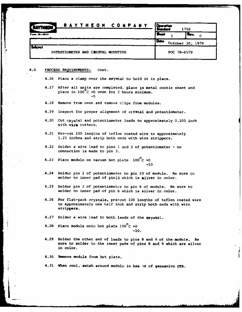
RA Y T H E0 N C 0 M P A Y
4 1758
43 0
_ _ _ _ _ _ _ _ Doe October 30,_1978
POTENTIOMETER AND CRYSTAL MOUNTING POC 78-6579
4.0 PROCESS REQUIREMENTS: Cont.
4.16 Place a clamp over the crystal. to hold it in place.
4.17 After all units are completed, place in metal cookie sheet andplace in 1000C +0 oven for 2 hours minimum.
-5
4.18 Remove from oven and remove clips from modules.
4.19 Inspect for proper alignment of crystal and potentiometer.
4.20 Cut crystal and potentiometer leads to approximately 0.100 inchwith wire cutters.
4.21 Pre-cut 100 lengths of teflon coated wire to approximately1.25 inches and strip both ends with wire strippers.
4.22 Solder a wire lead to pins 1 and 2 of potentiometer - noconnection is made to pin 3.
4.23 Place module on vacuum hot plate 100 C +0-10
4.24 Solder pin 1 of potentiometer to pin 10 of module. Be sure tosolder to inner pad of pinlo which is Silver in color.
4.25 Solder pin 2 of potentiometer to pin 6 of module. Be sure tosolder to inner pad of pin 6 which is silver in color.
4.26 For flat-pack crystals, pre-cut 100 lengths of teflon coated wireto approximately one half inch and strip both ends with wirestrippers.
4.27 Solder a wire lead to both leads of the crystal.
04.28 Place module onto hot plate 100 C +0-10.
4.29 Solder the other end of leads to pins 8 and 9 of the module. Besure to solder to the inner pads of pins 8 and 9 which are silverin color.
4.30 Remove module from hot plate.
4.31 When cool, swish around module in bea ir of genesolve DTA.
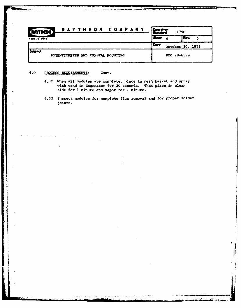
RAY HEO do 17ANY
,.n 0-004, 4 0 0" " ' ' ' ' DIN October 30, 1978
POTENTIOMETER AND CRYSTAL MOUNTING POC 78-6579
4.0 PROCESS REQUIREMENTS: Cont.
4.32 When all modules are complete, place in mesh basket and spraywith wand in degreaser for 30 seconds. Then place in cleanside for 1 minute and vapor for 1 minute.
4.33 Inspect modules for complete flux removal and for proper solderjoints.
i
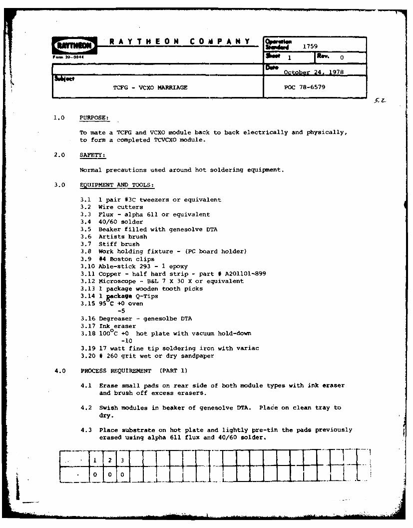
R A Y T H E 0 N C 0 At P A N Y z7
o... 20-0044 5W 1 0
_________-Oc___Otober 24, 1978
TCFG - VCXO MARRIAGE POC 78-6579
1.0 PURPOSE:
To mate a TCFG and VCXO module back to back electrically and physically,
to form a completed TCVCXO module.
2.0 SAFETY:
Normal precautions used around hot soldering equipment.
3.0 EQUIPMENT AND TOOLS:
3.1 1 pair #3C tweezers or equivalent3.2 Wire cutters3.3 Flux - alpha 611 or equivalent3.4 40/60 solder3.5 Beaker filled with genesolve DTA3.6 Artists brush3.7 Stiff brush3.8 Work holding fixture - (PC board holder)3.9 #4 Boston clips3.10 Able-stick 293 - 1 epoxy3.11 Copper - half hard strip - part # A201101-8993.12 Microscope - B&L 7 X 30 X or equivalent3.13 1 package wooden tooth picks3.14 1 gackage Q-Tips3.15 95 C +0 oven
-53.16 Degreaser - genesolbe DTA3.17 Ink eraser3.18 1000C +0 hot plate with vacuum hold-down
-103.19 17 watt fine tip soldering iron with variac3.20 # 260 grit wet or dry sandpaper
4.0 PROCESS REQUIREMENT (PART 1)
4.1 Erase small pads on rear side of both module types with ink eraserand brush off excess erasers.
4.2 Swish modules in beaker of genesolve DTA. Place on clean tray todry.
4.3 Place substrate on hot plate and lightly pre-tin the pads previouslyerased using alpha 611 flux and 40/60 solder.
1 2 3
o
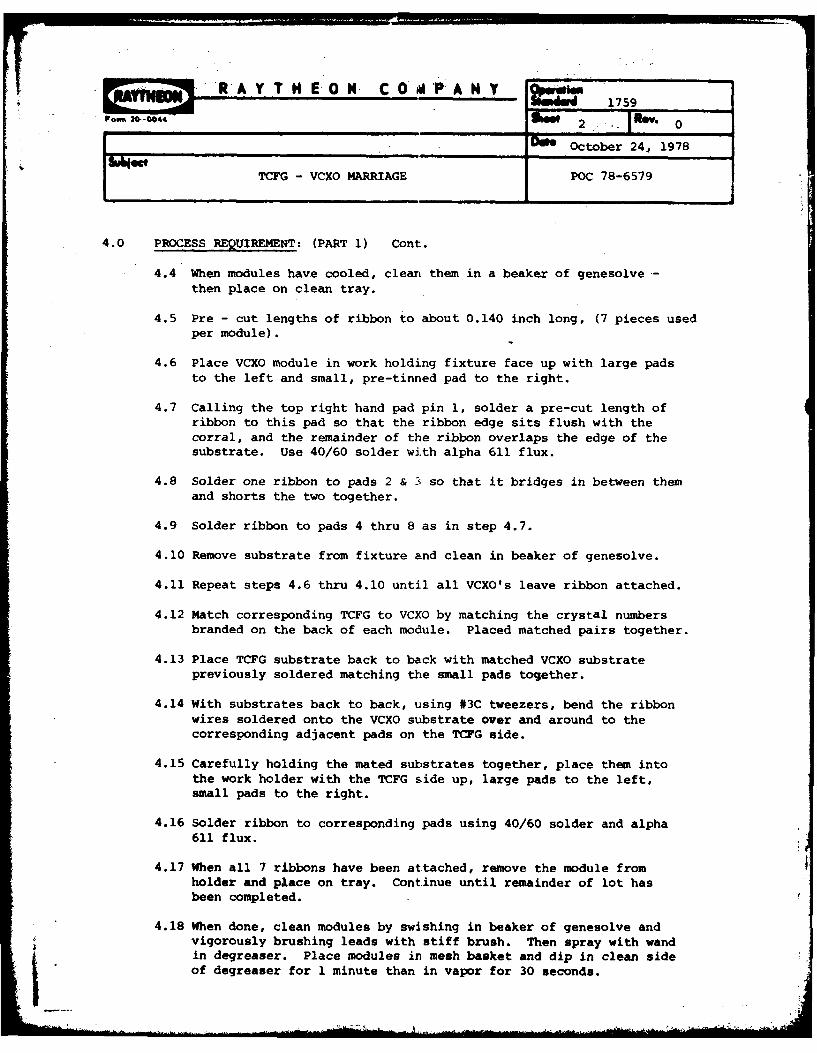
'RAY THEON. COMPAN Y_ ~ 15
ram 310-0044 2 - . 0
_-___October 24, 1978
TCFG - VCXO MARRIAGE POC 78-6579
4.0 PROCESS REQUIREMENT: (PART 1) Cont.
4.4 When modules have cooled, clean them in a beaker of genesolvethen place on clean tray.
4.5 Pre - cut lengths of ribbon to about 0.140 inch long, (7 pieces usedper module).
4.6 Place VCXO module in work holding fixture face up with large padsto the left and small, pre-tinned pad to the right.
4.7 Calling the top right hand pad pin 1, solder a pre-cut length ofribbon to this pad so that the ribbon edge sits flush with thecorral, and the remainder of the ribbon overlaps the edge of thesubstrate. Use 40/60 solder with alpha 611 flux.
4.8 Solder one ribbon to pads 2 & 3 so that it bridges in between themand shorts the two together.
4.9 Solder ribbon to pads 4 thru 8 as in step 4.7.
4.10 Remove substrate from fixture and clean in beaker of genesolve.
4.11 Repeat steps 4.6 thru 4.10 until all VCXO's leave ribbon attached.
4.12 Match corresponding TCFG to VCXO by matching the crystal numbersbranded on the back of each module. Placed matched pairs together.
4.13 Place TCFG substrate back to back with matched VCXO substratepreviously soldered matching the small pads together.
4.14 With substrates back to back, using #3C tweezers, bend the ribbonwires soldered onto the VCXO substrate over and around to thecorresponding adjacent pads on the TCFG side.
4.15 Carefully holding the mated substrates together, place them intothe work holder with the TCFG side up, large pads to the left,small pads to the right.
4.16 Solder ribbon to corresponding pads using 40/60 solder and alpha611 flux.
4.17 When all 7 ribbons have been attached, remove the module fromholder and place on tray. Continue until remainder of lot hasbeen completed.
4.18 When done, clean modules by swishing in beaker of genesolve andvigorously brushing leads with stiff brush. Then spray with wandin degreaser. Place modules in mesh basket and dip in clean side1* iof degreaser for 1 minute than in vapor for 30 seconds.
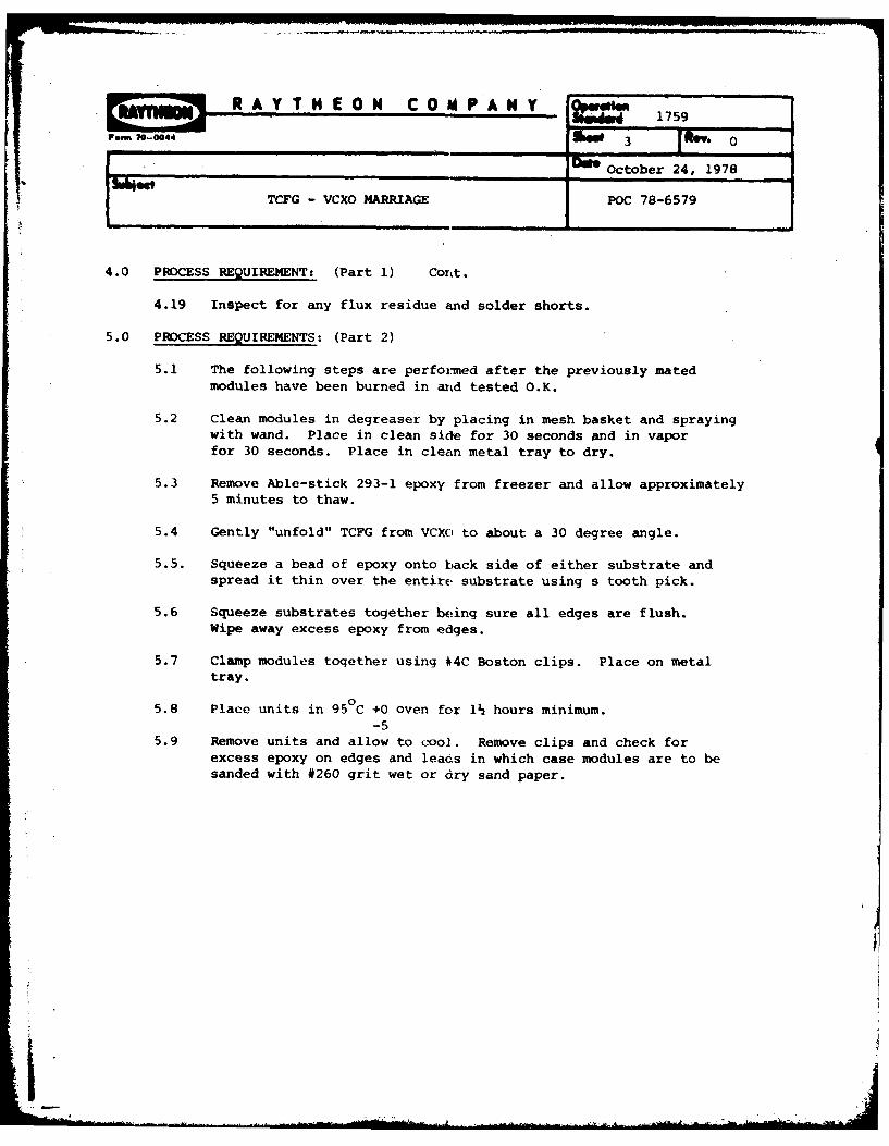
R A Y T H E 0 N C F 0 PA.I CO M N Y al 1759
r.o-o i004 3 Rev. 0
__________________________________Daft_ October 24, 1978
TCFG - VCXO MARRIAGE POC 78-6579
4.0 PROCESS REQUIREMENT: (Part 1) Cornt.
4.19 Inspect for any flux residue and solder shorts.
5.0 PROCESS REQUIREMENTS: (Part 2)
5.1 The following steps are performed after the previously matedmodules have been burned in and tested O.K.
5.2 Clean modules in degreaser by placing in mesh basket and sprayingwith wand. Place in clean side for 30 seconds And in vaporfor 30 seconds. Place in clean metal tray to dry.
5.3 Remove Able-stick 293-1 epoxy from freezer and allow approximately5 minutes to thaw.
5.4 Gently "unfold" TCFG from VCXO to about a 30 degree angle.
5.5. Squeeze a bead of epoxy onto back side of either substrate andspread it thin over the entire substrate using s tooth pick.
5.6 Squeeze substrates together being sure all edges are flush.Wipe away excess epoxy from edges.
5.7 Clamp modules toqether using 44C Boston clips. Place on metaltray.
5.8 Place units in 950C +0 oven for 12 hours minimum.-5
5.9 Remove units and allow to cool. Remove clips and check forexcess epoxy on edges and leads in which case modules are to besanded with #260 grit wet or dry sand paper.
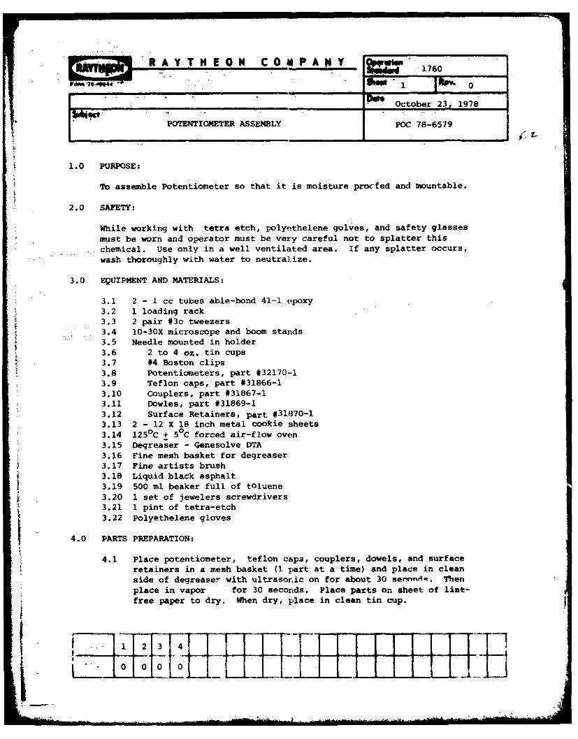
A VT H 1 E 0 N C 0 M P A Y 1
_______________________________________ October_23,_1978
POTENTIOMETER ASSEMBLY POC 78-6579
1.0 PURPOSE:
To assemble Potentiometer so that it is moisture procfed and mountable.iK
2.0 SAFETY:
While working with tetra etch, polyethelene golves, and safety glassesmust be worn and operator must be very careful not to splatter thischemical. Use only in a well ventilated area. If any splatter occurs,wash thoroughly with water to neutralize.
3.0 EQUIPMENT AND MATERIALS:
3.1 2 - 1 cc tubes able-bond 41-1 epoxy3.2 1 loading rack3.3 2 pair #3c tweezers3.4 10-30X microscope and boom stands3.5 Needle mounted in holder3.6 2 to 4 oz. tin cups3.7 #4 Boston clips3.8 Potentiometers, part #32170-13.9 Teflon caps, part #31866-13.10 Couplers, part #31867-1
* 3.11 Dowles, part #31869-13.12 Surface Retainers, part #31870-13.13 2 - 12 X 18 inch metal cookie sheets
03.14 1250C + 5 C forced air-flow oven3.15 Degreaser - Genesolve DTA3.16 Fine mesh basket for degreaser3.17 Fine artists brush3.18 Liquid black asphalt3.19 500 ml beaker full of toluene3.20 1 set of jewelers screwdrivers3.21 1 pint of tetra-etch3.22 Polyethelene gloves
4.0 PARTS PREPARATION:
4.1 Place potentiometer, teflon caps, couplers, dowels, and surfaceretainers in a mesh basket (1 part at a time) and place in cleanside of degreaser with ultrasonic on for about 30 emnna. Thenplace in vapor for 30 seconds. Place parts on sheet of 1int-free paper to dry. When dry, place in clean tin cup.
1 2 30 _ ..
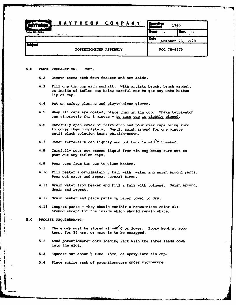
1760
om20- 0044 2 0e
. , October 23, 1978
P OTE NTIONETER ASSEMBLY POC 78-6579
4.0 PARTS PREPARATION: Cont.
4.2 Remove tetra-etch from freezer and set aside.
4.3 Fill one tin cup with asphalt. With artists brush, brush asphalton inside of teflon cap being careful not to get any onto bottomlip of cap.
4.4 Put on safety glasses and ployethelene gloves.
4.5 When all caps are coated, place them in tin cup. Shake tetra-etchcan vigorously for 1 minute - be sure cup is tightly closed.
4.6 Carefully open cover of tetra-etch and pour over caps being sureto cover them completely. Gently swish around for one minuteuntil black solution turns whitish-brown.
4.7 Cover tetra-etch can tightly and put back in -40°C freezer.
4.8 Carefully pour out excess liquid from tin cup being sure not topour out any teflon caps.
4.9 Pour caps from tin cup to glass. beaker.
4.10 Fill beaker approximately full with water and swish around parts.Pour out water and repeat several times.
4.11 Drain water from beaker and fill k full with toluene. Swish around,
drain and repeat.
4.12 Drain beaker and place parts on paper towel to dry.
4.13 Inspect parts - they should exhibit a brown-black color allaround except for the inside which should remain white.
5.0 PROCESS REQUIREMENTS:
05.1 The epoxy must be stored at -40 C or lower. Epoxy kept at room
temp. for 24 hrs. or more is to be scrapped.
5.2 Load potentiometer onto loading rack with the three leads downinto the slot.
5.3 Squeeze out about tube ( cc,' of epoxy into tin cup.
5.4 Place entire rack of potentiometers under microscope.
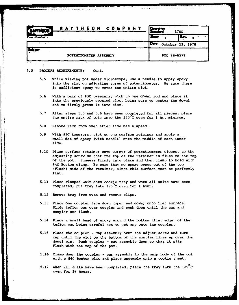
1760
3 No. 0
October 23, 1978
POTENTIOMETER ASSEMBLY POC 78-6579
5.0 PROCESS REQUIREMENTS: Cont.
5.5 While viewing pot under microscope, use a needle to apply epoxyinto the slot on adjusting screw of potentiometer. Be sure thereis sufficient epoxy to cover the entire slot.
5.6 With a pair of #3C tweezers, pick up one dowel rod and place itinto the previously epoxied slot, being sure to center the doweland to firmly press it into slot.
5.7 After steps 5.5 and 5.6 have been completed for all pieces, place
the entire rack of pots into the 125°C oven for 1 hr. minimum.
5.8 Remove rack from oven after time has elapsed.
5.9 With #3C tweezers, pick up one surface retainer and apply asmall dot of epoxy (with needle) onto the middle of each innerside.
5.10 Place surface retainer onto corner of potentiometer closest to theadjusting screw so that the ton of the retainer is flush to the topof the pot. Squeeze firmly into place and then clamp to hold with#4C Boston clamp. Be sure that no epoxy oozes out of the top(flush) side of the retainer, since this surface must be perfectlyflat.
5.11 Place clamped unit onto cookie tray and when all units have beencompleted, put tray into 125 0C oven for 1 hour.
5.12 Remove tray from oven and remove clips.
5.13 Place one coupler face down (open end down) onto flat surface.Slide teflon cap over coupler and push down until the cap andcoupler are flush.
5.14 Place a small bead of epoxy around the bottom (flat edge) of theteflon cap being careful not to get any onto the coupler.
5.15 Place the coupler - cap assembly over the adjust screw and turncap until the slot on the bottom of the coupler lines up over thedowel pin. Push coupler - cap assembly down so that it sitsflush with the top of the pot.
5.16 Clamp down the coupler - cap assembly to the main body of the potwith a #4C Boston clip and place assembly onto a cookie sheet.
5.17 When all units have been completed, place the tray into the 125 0Coven for 2N hours.
1760
___ ___ __ ___ ___ _ October 23, 1978
POTENTIOMETER ASSEMBLY POC 78-6579
5.0 PROCESS REQUIREMENTS: Cont.
5.18 Remove tray from oven and remove clips.
5.19 Inspect assemblies, looking for misalligned cups.
5.20 With a jewelers screwdriver, turn the set screw inside the tefloncup. If it does not turn, the assembly is no good and should bescrapped.
-- * .....-
Ponm 20-0044 b 1 N - 0
_ _._ _....._ _ _ __ October 18, 1978
POC 78-6564BURN IN PROCEDURE FOR ECOM MODULES H60388
1.0 EQUIPMENT:
1.1 50 socket burn in tray drawing C78-59-E1.
1.2 Blue-M Burn in oven
1.3 Sorensen power type ORD15-2 or equivalent.
2,0 SET UP PROCEDURE:
2.1 Adjust power supply for 412.OV
2.2 Switch off power supplv
2.3 Plug modules into tray making sure thaL each socket in theburn in tray is fitted with a fiber qlass spacer. This spacershould be positioned to block off the two left side terminalslooking at the front of the tray.
2,4 Slide burn in tray into slides in oven so that the rearconnector on the tray is engaged in the oven socket.
2.5 Switch on 12V power supply and confirm voltage setting iscorrect by monitoring pin 5 on any of the module socket -back row left hand side looking at top of tray. Readjustif necessary.
2.6 Close up oven, set for 125°C and switch on.
N = 7 1762
Fon 20-0044 1 0
Feb. 19, 1979INSPECTION OF ECOM MODULES TCVCXO POC 79-6112
H60388
1.0 PURPOSE:
The purpose of this instruction is to provide criteria for the inspectionof TCVCXO modules. Para. 5.0 Pre-Pot. Para. 6.0 Final Q.C. Inspection.
2.0 FREQUENCY:
All (100%) modules shall be inspected.
3.0 EQUIPMENT:
lOX magnification as required, calipers or spacers.
4.0 PRE-INSPECTION PERUSAL:
Referring to the applicable assembly drawing check to assure that allcomponents and connections are in their proper location. Check toassure that all bond Prdia have been cured (soft or tacky epoxyis not acceptable). Components or wires may not appear damaged, seperatedor broken.
5.0 PRE-POT INSPECTION CRITERIA:
5.1 Soldering criteria shall be as specified in paragraph 4.2.1 ofO.S. 1265, except as modified in paragraphs below.
5.2 Spacing Requirements:
5.2.1 Potentiometer leads must be maintained at least .010"above case.
5.2.2 The end of the potentiometer shall be flush with the edgeof the substrate within .005".
5.2.3 The potentiometer shall be positioned as per dimensionsindicated on Assy. Drawing 31380.
5.2.4 With the module lying flat, the projection of the crystaland potentiometer wires shall not extend beyond the die-electric line printed on the terminals. (Drawing 31380)
5.2.5 Crystals shall be positioned as per dash number type withref. to drawing 31380.
0 0 0 0 0
~~~R A Y T H E 0 N C 0 M P A N Y 16
2:= 1762,o,2-0,, 4w4t 2 j- . 0
NFeb. 19, 1979INSPECTION OF ECOM MODULES TCVCXO POC 79-6112
H60388
5.2 Spacing Requirements: Cont.
5.2.6 All crystals shall be centered with respect to the width of
the substrate as per drawing 31380 dimensions.
5.2.7 Edges of back to back substrates shall be flush within .010".
5.2.8 A .005" spacing must be maintained between conductor terminalson the wrap-around end.
5.2.9 Crystal Mounting:
5.2.9.1 T05 type crystals must be mounted in the hole of thespecified spacer with the leads parallel to the edgeof substrate. Ref. Drawing 31380.
5.2.9.2 Ceramic type crystals must be mounted to spacer with-out hole. Ref. Drawing 31380.
5.2.9.3 Crystal-can type crystals shall be mounted to spacerwithout hole. Ref. Drawing 31380.
5.2.10 Miscellaneous:
5.2.10.1 There shall be no evidence of peeling blistered orcut metalization.
5.2.10.2 There shall be no epoxy on edge surfaces of substrateor extending on any lead surface.
5.2.10.3 Substrates must be free of chip outs or cracks asviewed under lOX magnification.
5.2.10.4 All crystal and potentiometer leads shall be insulatedwith a sleeve.
5.2.10.5 Solder on long terminals shall not extend beyond whitedielectric line printed on the terminals.
5.2.10.6 The crystal number shall be indicated on the white labelattached to the crystal and also scribed into the VCXOcover next to the potentiometer.
NOTE: This number also serves as the module serial number.
5.2.10.7 Covers may not appear dented, distorted or otherwisedamaged.
...Ii" ..... . . 'f ' ell [ .- I ..
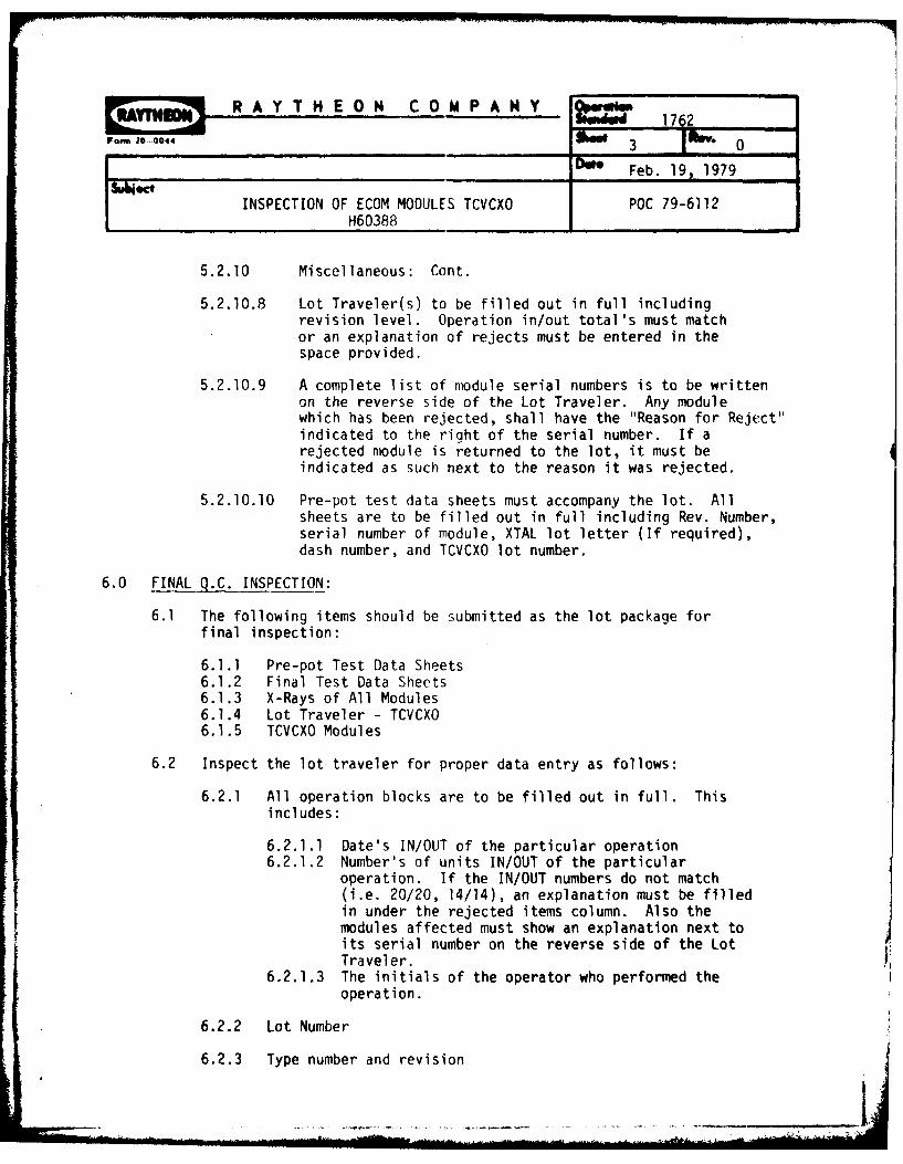
Pam 20-0044 owe
Doe Feb. 19, 1979
INSPECTION OF ECOM MODULES TCVCXO POC 79-6112H60388
5.2.10 Miscellaneous: Cont.
5.2.10.8 Lot Traveler(s) to be filled out in full includingrevision level. Operation in/out total's must matchor an explanation of rejects must be entered in thespace provided.
5.2.10.9 A complete list of module serial numbers is to be writtenon the reverse side of the Lot Traveler. Any modulewhich has been rejected, shall have the "Reason for Reject"indicated to the right of the serial number. If arejected module is returned to the lot, it must beindicated as such next to the reason it was rejected.
5.2.10.10 Pre-pot test data sheets must accompany the lot. Allsheets are to be filled out in full including Rev. Number,serial number of module, XTAL lot letter (If required),dash number, and TCVCXO lot number.
6.0 FINAL Q.C. INSPECTION:
6.1 The following items should be submitted as the lot package forfinal inspection:
6.1.1 Pre-pot Test Data Sheets6.1.2 Final Test Data Sheets6.1.3 X-Rays of All Modules6.1.4 Lot Traveler - TCVCXO6.1.5 TCVCXO Modules
6.2 Inspect the lot traveler for proper data entry as follows:
6.2.1 All operation blocks are to be filled out in full. Thisincludes:
6.2.1.1 Date's IN/OUT of the particular operation6.2.1.2 Number's of units IN/OUT of the particular
operation. If the IN/OUT numbers do not match(i.e. 20/20, 14/14), an explanation must be filledin under the rejected items column. Also themodules affected must show an explanation next toits serial number on the reverse side of the LotTraveler.
6.2.1.3 The initials of the operator who performed theoperation.
6.2.2 Lot Number
6.2.3 Type number and revision
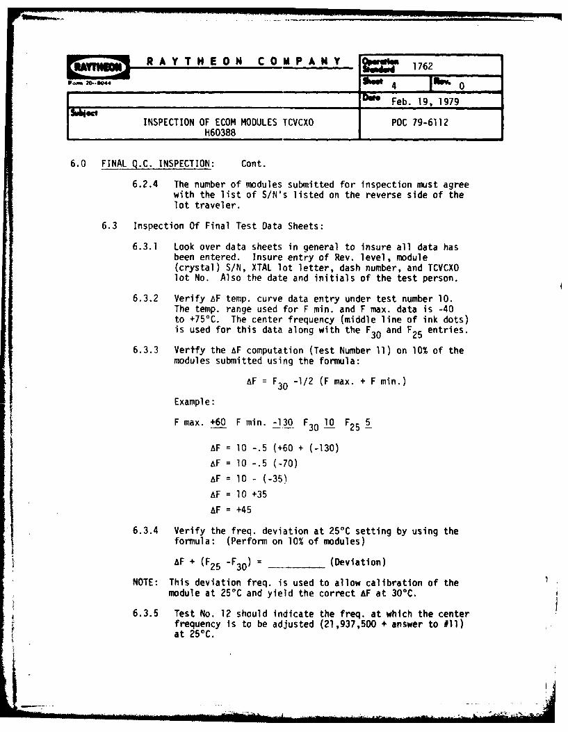
R A Y T H E 0 N C 0 ¥ P A N Y 161762
Dole Feb. 19, 1979
INSPECTION OF ECOM MODULES TCVCXO POC 79-6112H60388
6.0 FINAL Q.C. INSPECTION: Cont.
6.2.4 The number of modules submitted for inspection must agreewith the list of S/N's listed on the reverse side of thelot traveler.
6.3 Inspection Of Final Test Data Sheets:
6.3.1 Look over data sheets in general to insure all data hasbeen entered. Insure entry of Rev. level, module(crystal) S/N, XTAL lot letter, dash number, and TCVCXOlot No. Also the date and initials of the test person.
6.3.2 Verify AF temp. curve data entry under test number 10.The temp. range used for F min. and F max. data is -40to +75°C. The center frequency (middle line of ink dots)is used for this data along with the F30 and F25 entries.
6.3.3 Verify the AF computation (Test Number 11) on 10% of themodules submitted using the formula:
AF = F30 -1/2 (F max. + F min.)
Example:
F max. +60 F min. -130 F30 LO F25 5
AF = 10 -.5 (+60 + (-130)
AF = 10 -.5 (-70)
AF = 10 - (-35)
AF = 10 +35
AF = +45
6.3.4 Verify the freq. deviation at 25C setting by using theformula: (Perform on 10% of modules)
AF + (F2 5 -F30) = (Deviation)
NOTE: This deviation freq. is used to allow calibration of themodule at 25C and yield the correct AF at 300C.
6.3.5 Test No. 12 should indicate the freq. at which the centerfrequency is to be adjusted (21,937,500 + answer to #11)at 25*C.
.... . ...... ~ l ............... .. n]i i -
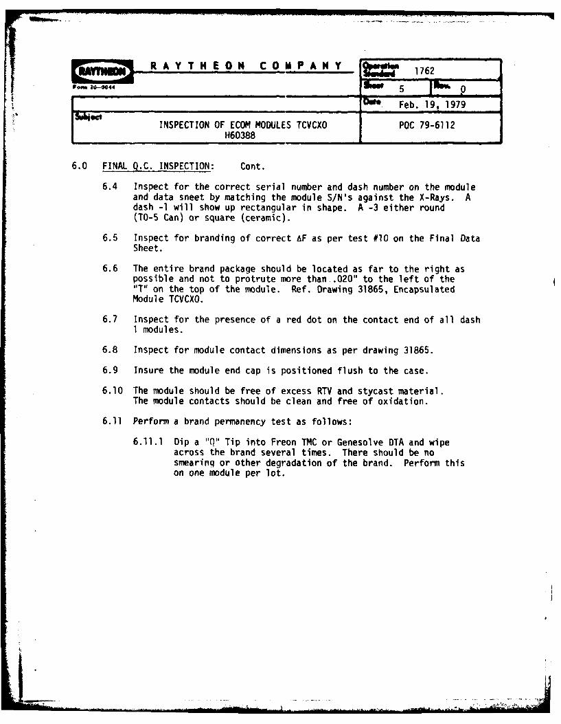
IIAlflIIIII R A Y T H E 0 N C 0 M P A N Y '16_..1762
ro 004sei 5 0____ _ Feb. 19, 1979
INSPECTION OF ECOM MODULES TCVCXO POC 79-6112H60388
6.0 FINAL Q.C. INSPECTION: Cont.
6.4 Inspect for the correct serial number and dash number on the moduleand data sneet by matching the module S/N's against the X-Rays. Adash -1 will show up rectangular in shape. A -3 either round(TO-5 Can) or square (ceramic).
6.5 Inspect for branding of correct AF as per test #10 on the Final DataSheet.
6.6 The entire brand package should be located as far to the right aspossible and not to protrute more than.020" to the left of the"T" on the top of the module. Ref. Drawing 31865, EncapsulatedModule TCVCXO.
6.7 Inspect for the presence of a red dot on the contact end of all dash
1 modules.
6.8 Inspect for module contact dimensions as per drawing 31865.
6.9 Insure the module end cap is positioned flush to the case.
6.10 The module should be free of excess RTV and stycast material.The module contacts should be clean and free of oxidation.
6.11 Perform a brand permanency test as follows:
6.11.1 Dip a "Q" Tip into Freon TMC or Genesolve DTA and wipeacross the brand several times. There should be nosmearing or other degradation of the brand. Perform thison one module per lot.
............................................y.
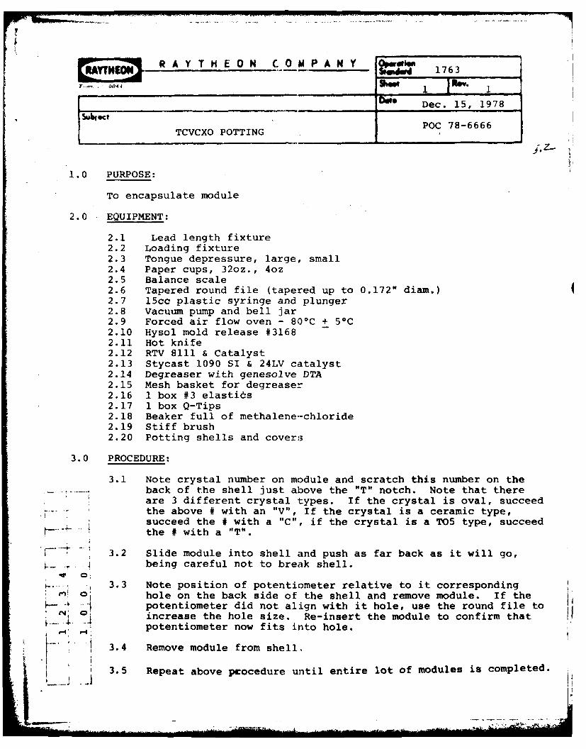
R A Y T H E 0 N C 0 M P A N Y 16
.T... MY 7 1763
4Dec. 15, 1978
SAJ~ctPOC 78-6666TCVCXO POTTING
1.0 PURPOSE:
To encapsulate module
2.0 EQUIPMENT:
2.1 Lead length fixture2.2 Loading fixture2.3 Tongue depressure, large, small2.4 Paper cups, 32oz., 4oz2.5 Balance scale2.6 Tapered round file (tapered up to 0.172" diam.)2.7 15cc plastic syringe and plunger2.8 Vacuum pump and bell jar2.9 Forced air flow oven - 80C + 5C2.10 Hysol mold release #31682.11 Hot knife2.12 RTV 8111 & Catalyst2.13 Stycast 1090 SI & 24LV catalyst2.14 Degreaser with genesolve DTA2.15 Mesh basket for degreaser2.16 1 box #3 elastics2.17 1 box Q-Tips2.18 Beaker full of methalene-chloride2.19 Stiff brush2.20 Potting shells and covers
3.0 PROCEDURE:
3.1 Note crystal number on module and scratch this number on theback of the shell just above the "T" notch. Note that thereare 3 different crystal types. If the crystal is oval, succeed
... .the above # with an "V", If the crystal is a ceramic type,succeed the # with a "C", if the crystal is a T05 type, succeedthe # with a "T".
3.2 Slide module into shell and push as far back as it will go,. being careful not to break shell.
.3.3 Note position of potentiometer relative to it correspondinghole on the back side of the shell and remove module. If the
potentiometer did not align with it hole, use the round file toincrease the hole size. Re-insert the module to confirm thatpotentiometer now fits into hole.
4 3.4 Remove module from shell.
- 3.5 Repeat above pcocedure until entire lot of modules is completed..Lif.
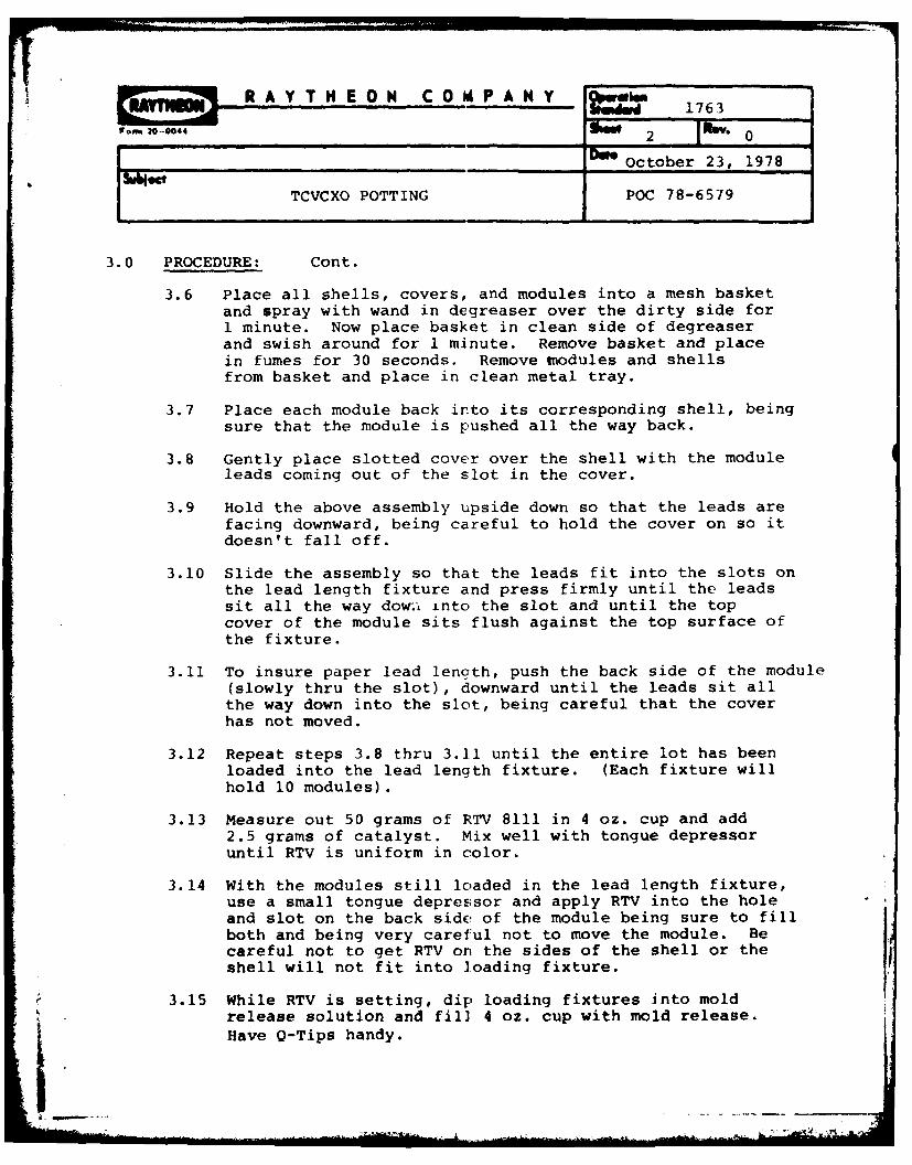
R A Y T H E 0 N C 0 M P A N Y 1763
Orm 0- 044 2 7 7
' _ _ _ _ _ _ _ __..... . .. ... _ D October 23, 1978
TCVCXO POTTING POC 78-6579
3.0 PROCEDURE: Cont.
3.6 Place all shells, covers, and modules into a mesh basketand spray with wand in degreaser over the dirty side for1 minute. Now place basket in clean side of degreaserand swish around for 1 minute. Remove basket and placein fumes for 30 seconds. Remove modules and shellsfrom basket and place in clean metal tray.
3.7 Place each module back into its corresponding shell, beingsure that the module is pushed all the way back.
3.8 Gently place slotted cover over the shell with the moduleleads coming out of the slot in the cover.
3.9 Hold the above assembly upside down so that the leads arefacing downward, being careful to hold the cover on so itdoesn't fall off.
3.10 Slide the assembly so that the leads fit into the slots onthe lead length fixture and press firmly until the leadssit all the way dow 1 into the slot and until the topcover of the module sits flush against the top surface ofthe fixture.
3.11 To insure paper lead lenath, push the back side of the module(slowly thru the slot), downward until the leads sit allthe way down into the slot, being careful that the coverhas not moved.
3.12 Repeat steps 3.8 thru 3.11 until the entire lot has beenloaded into the lead length fixture. (Each fixture willhold 10 modules).
3.13 Measure out 50 grams of RTV 8111 in 4 oz. cup and add2.5 grams of catalyst. Mix well with tongue depressoruntil RTV is uniform in color.
3.14 With the modules still loaded in the lead length fixture,use a small tongue depressor and apply RTV into the holeand slot on the back side of the module being sure to fillboth and being very careful not to move the module. Becareful not to get RTV on the sides of the shell or theshell will not fit into loading fixture.
3.15 While RTV is setting, dip loading fixtures into moldrelease solution and fill 4 oz. cup with mold release.Have Q-Tips handy.
.
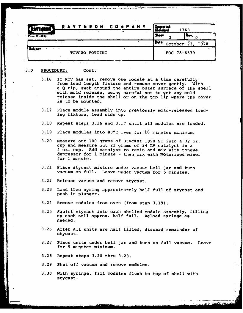
17633 10;7
-October 23, 198
TCVCXO POTTING POC 78-6579
3.0 PROCEDURE: Cont.
3.16 If RTV has set, remove one module at a time carefullyfrom lead length fixture and remove cover gently. Witha Q-tip, swab around the entire outer surface of the shellwith mold release, being careful not to get any moldrelease inside the shell or on the top lip where the coveris to be mounted.
3.17 Place module assembly into previously mold-released load-ing fixture, lead side up.
3.18 Repeat steps 3.16 and 3.17 until all modules are loaded.
3.19 Place modules into 80*C oven for 10 minutes minimum.
3.20 Measure out 100 grams of Stycast 1090 SI into a 32 oz.cup and measure out 23 grams of 24 LV catalyst in a4 oz. cup. Add catalyst to resin and mix with tonguedepressor for 1 minute - then mix with motorized mixerfor 1 minute.
3.21 Place stycast mixture under vacuum bell jar and turnvacuum on full. Leave under vacuum for 5 minutes.
3.22 Release vacuum and remove stycast.
3.23 Load 15cc syring approximately half full of stycast andpush in plunger.
3.24 Remove modules from oven (from step 3.19).
3.25 Squirt stycast into each shelled module assembly, fillingup each sell approx. half full. Reload syringe asneeded.
3.26 After all units are half filled, discard remainder ofstycast.
3.27 Place units under bell jar and turn on full vacuum. Leavefor 5 minutes minimum.
3.28 Repeat steps 3.20 thru 3.23.
3.29 Shut off vacuum and remove modules.
3.30 With syringe, fill modules flush to top of shell withstycast.
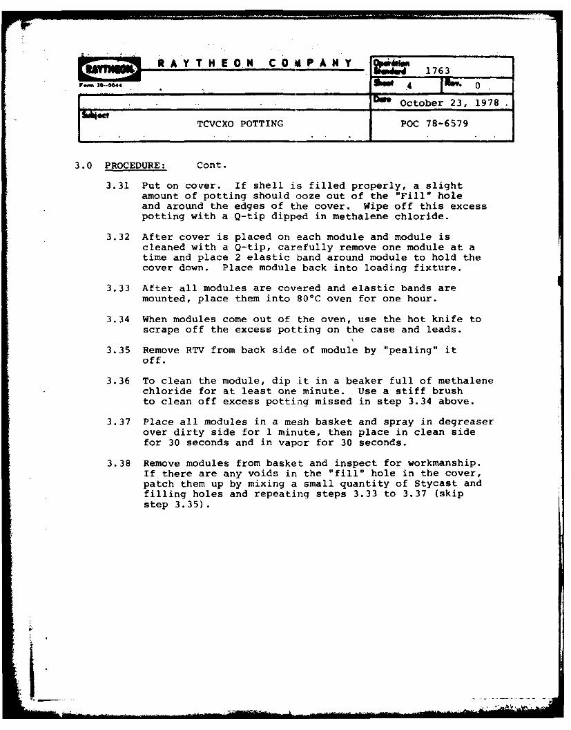
NN 4 *0
____________________________Doe_
October_23,_1978-lTCVCXO POTTING POC 78-6579
3.0 PROCEDURE: Cont.
3.31 Put on cover. If shell is filled properly, a slightamount of potting should ooze out of the "Fill" holeand around the edges of the cover. Wipe off this excesspotting with a Q-tip dipped in methalene chloride.
3.32 After cover is placed on each module and module iscleaned with a Q-tip, carefully remove one module at atime and place 2 elastic band around module to hold thecover down. Place module back into loading fixture.
3.33 After all modules are covered and elastic bands aremounted, place them into 80'C oven for one hour.
3.34 When modules come out of the oven, use the hot knife toscrape off the excess potting on the case and leads.
3.35 Remove RTV from back side of module by "pealing" itoff.
3.36 To clean the module, dip it in a beaker full of methalenechloride for at least one minute. Use a stiff brushto clean off excess potting missed in step 3.34 above.
3.37 Place all modules in a mesh basket and spray in degreaserover dirty side for 1 minute, then place in clean sidefor 30 seconds and in vapor for 30 seconds.
3.38 Remove modules from basket and inspect for workmanship.If there are any voids in the "fill" hole in the cover,patch them up by mixing a small quantity of Stycast andfilling holes and repeating steps 3.33 to 3.37 (skipstep 3.35).
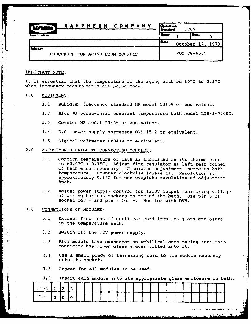
UP!H R A Y T H E 0 N C 0 M P A N Y 1765
Foe 20 "0044 S 1765
D___October 17, 1978
PROCEDURE FOR AGING ECOM MODULES POC 78-6565
IMPORTANT NOTE:
It is essential that the temperature of the aging bath be 600 C to 0.10C
when frequency measurements are being made.
1.0 EQUIPMENT:
1.1 Rubidium frequency standard HP model 5065A or equivalent.
1.2 Blue N1 versa-whirl constant temperature bath model LTB-l-P200C.
1.3 Cotinter HP model 5345A or equivalent.
1.4 D.C. power supply sorrensen QRD 15-2 or equivalent.
1.5 Digital voltmeter HP3439 or equivalent.
2.0 ADJUSTMENTS PRIOR TO CONNECTING MODULES:
2.1 Confirm temperature of bath as indicated on its thermometeris 60.0'C + 0.10 C. Adjust fine regulator at left rear cornerof bath when necessary. Clockwise adjustment increases bathtemperature. Counter clockwise lowers it. Resolution isapproximately 0.5*C for one complete revolution of adjustmentknob.
2.2 Adjust power suppl' control for 12.0V output monitoring voltaqeat wiring harness sockets on top of the bath. Use pin 5 ofsocket for + and pin 3 for -. Monitor with DVM.
3.0 CONNECTIONS OF MODULES:
3.1 Extract free end of umbilical cord from its glass enclosurein the temperature bath.
3.2 Switch off the 12V power supply.
3.3 Plug module into connector on umbilical cord making sure thisconnector has fiber glass spacer fitted into it.
3.4 Use a small piece of harressing cord to tie module securelyonto its socket.
3.5 Repeat for all modules tc be used.
3.6 Insert each module into its appropriate glass enclosure in bath.
* .' I, 1 2 3i 0 0
•m 0-0-...,- 2 lft"- 0__... ... . October_17,_1978
PROCEDURE FOR AGING ECOM MODULES POC 78-6565
4.0 TESTING MODULES IN AGING BATH:
4.1 Switch on +12V power supply.
4.2 Monitor pin I at each of the sockets in the wiring harness onthe top nf the bath which have modules connected to theirumbilical cords with the DVM. Voltage must be 9.OV + 0.1V.
4.3 Connect 5MHZ signal output from rubidium frequency standardto external frequency standard input BNC Jack at rear ofcounter.
4.4 Use counter to monitor each module frequency and record onData Sheet together with its lot and serial number.
4.5 Repeat 4.4 every 24 hours during the aging cycle.
I
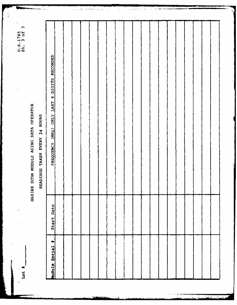
.w 0cn~
0
E-.
o 5
<u
z
z
z~00 H
Z In4:
co
mm
r41 01
z U )
V-4
0 *
.,G 064 9i. ... "W 1 1 ItvDe December 5, 1978
BRANDING OF TCVCXO POC 78-6640
1.0 PURPOSE:
To define a process for applying and curing of branding ink to TCVCXOfinal assembly.
2.0 EQUIPMENT AND MATERIALS:
2.1 Hand stamp, Pullman XCPN - 009 or equivalent
2.2 Flat rubber stamp pad made according to print #32561
2.3 Plate glass of convenient size (at least 1 foot sq.), mounted ontable top.
2.4 Standard rojafix ink roller
2.5 Raytheon Ink, Red #ZZIO-2 (303450-5)
2.6 Raytheon Ink, White #ZZ1O-9 (303450-19)
2.7 Morkem #320 cleaner
2.8 Lint-free cloth
2.9 1000C +0 oven-5
2.10 Double sided stick tape
2.11 Finger cots
2.12 Metal cookie sheet - 12 X 18 inches
3.0 CLEANING BEFORE BRANDING:
3.1 Operator must wear finger cots while cleaning and branding.
3.2 Using a clean, lint-free cloth, wipe surface to be branded withmorkem #320 cleaner.
3.3 After cleaner has evaporated, repeat step 3.2 with clean cloth.
3.4 Modules should be branded soon after cleaner evaporates.
i 2
R H E 0 N C 00 ww
~~jY N E O N ~ M PA Y ~ n 1766
Date December 5,7
BRANDING OF TCVCXO POC 78-6640
4.0 APPLICATION OF BRAND:
4.1 Apply double - sided stick tape to back side of rubber stamp andstick stamp onto glass table top.
4.2 Place a small amount of ink onto the glass plate and roll to aneven layer.
4.3 After rolling over the ink with roller, roll over the rubber stamp,being sure to cover all numbers uniformly with ink. If coverageis not uniform, wipe stamp with cloth wet with m kem cleaner andre-roll with ink.
4.4 Grasp TCVCXO module with both hands and roll it over the rubberstamp so that the brand is oriented as shown on the final assemblyprint #31865-2.
4.5 If, after rolling, the brand is too thick or mis-oriented, wipe itoff with a cloth wet with markem cleaner and re-brand after cleanerevaporates.
4.6 Using a Pullman XCPN - 009 hand stamp, or equivalent, stamp in datecode, type number (-I or -3) and serial number. Note: If module isa type -1, the -l is to be branded in red along with a red dot onthe rear of the module as shown on print #31865-2.
4.7 After all modules are complete, place on a clean metal cookie sheetand place in a 1000C +0 oven for 2 hours minimum.
-54.8 Modules are now ready to submit to Final Test.
4.9 After modules have been final tested, a sheet of "deltas" will besubmitted with the lot to the brander. Brand the delta to thecorresponding module in the space provided. (See print #31865-2)
4.10 Cure as in step 4.7.
4.11 All branding is now completed and modules should be submitted toQ.C. for inspection.
ELECTRONICS TECHNOLOGY AND DEVICES LABORATORY
MANDATORY CONTRACT DISTRIBUTION LIST
101 Defense Technical Information CenterATTN: DTIC-TCACameron Station (BLDG 5)
012 Alexandria, VA 22314
203 GIDEP Engineering & Support DeptTE SectionPO Box 398
001 NORCO, Ca 91760
205 DirectorNaval Research LaboratoryATTN: CODE 2627
001 Washington, DC 20375
301 Rome Air Development CenterATTN: Documents Library (TILD)
001 Griffiss AFB, NY 13441
437 Deputy for Science & TechnologyOffice, Asst Sec Army (R&D)
001 Washington, DC 20310
438 HQDA (DAMA-ARZ-D/Dr. F. D. Verderame)001 Washington, DC 20310
482 DirectorUS Army Materiel Systems Analysis ActvATTN: DRXSY-T
001 Aberdeen Proving Ground, MD 21005
563 Commander, DARCOMATTN: DRCDE5001 Eisenhower Avenue
001 Alexandria, VA 22333
564 Cdr, US Army Signals Warfare LabATTN: DELSW-OSVint Hill Farms Station
001 Warrenton, VA 22186
579 Cdr. PM Concept Analysis CentersATTN: DRCPM-CACArlington Hall Station
001 Arlington, VA 22212
ELECTRONICS TECHNOLOGY AND DEVICES LABORATORY
MANADATORY CONTRACT DISTRIBUTION LIST (CONT'D)
602 Cdr, Night Vision & Electro-OpticsERADCOMATTN: DELNV-D
001 Fort Belvoir, VA 22060
603 Cdr, Atmospheric Sciences LabERADCOMATTN: DELAS-SY-S
001 White Sands Missile Range, NM 88002
607 Cdr, Harry Diamond LaboratoriesATTN: DELHD-CO, TD (In Turn)2800 Powder Mill Road
001 Adelphi, MD 20783
609 Cdr, ERADCOMATTN: DRDEL-CG, CD, CS (In Turn)2800 Powder Mill Road
001 Adelphi, MD 20783
612 Cdr, ERADCOMATTN: DRDEL-CT2800 Powder Mill Road
001 Adelphi, MD 20783
680 CommanderUS Army Electronics R&D Command
000 Fort Monmouth, NJ 077031 DELET-IT (O.P. Layden)1 DELEW-D1 DELET-DD1 DELSD-L (Tech Library)2 DELSD-L-S (STINFO)5 Originating Office (DELET-MF)1 DELET-MQ (J. VIG)1 DELET-MF (S. Schodowski)
681 CommanderUS Army Communications R&D CommandATTN: USMC-LNO
001 Fort Monmouth, NJ 07703
ELECTRONICS TECHNOLOGY AND DEVICES LABORATORY
MANDATORY CONTRACT DISTRIBUITON LIST (CONT'D)
705 Advisory Group on Electron Devices201 Varick Street, 9th Floor
002 New York City, NY 10014
Project Manager Firefinder/RembassFort Monmouth, NJ 07703DRCPM-FFR
002 ATTN: H. Mazurczyk
DirectorUS Army Industrial Base Engineering ActivityRock Island ArsenalRock Island, IL 61201
001 ATTN: DRXIB-MT (Mr. C. McBurney)
RCA/Government and Commercial SystemsP.O. Box 588Burlington, MA 01803
001 ATTN: E. Waldron
Motorola, Inc.2553 N. Edgington StreetFranklin Park, IL 60131
001 ATTN: D. Reifel
General Electric Neutron Devices DeptP.O. Box 11508St. Petersburg, FL 33733
001 ATTN: R. Ney
Honeywell, Inc.13350 US19St. Petersburg, FL 33733
001 ATTN: P. Miranda
.|ff= A'