Embed Size (px)
Citation preview
Identification of skill needsin nanotechnology
TI-73-06-631-EN-C
EN
Europe 123, GR-570 01 Thessaloniki (Pylea)Postal address: PO Box 22427, GR-551 02 ThessalonikiTel. (30) 23 10 49 01 11, Fax (30) 23 10 49 00 20E-mail: [email protected]: www.cedefop.eu.intInteractive website: www.trainingvillage.gr
European Centre for theDevelopment of Vocational Training
Free of charge – On request from Cedefop
Identification of skill needs in nanotechnology
5170 EN
ISBN 92-896-0429-8
The development of nanotechnology is often considered as a fundamental rev-olution in technology and compared with the discovery of antibiotics, televisionor computer technologies. Nanotechnology is expected to generate great oppor-tunities not only for science and research but also for manufacturing and poten-tially for the every-day life of people. Which skills and qualifications will be indemand in the future?This publication reviews recent developments and trends in different fields ofnanotechnology and their related skill needs. The study was also presented asa keynote contribution to the international workshop ‘Emerging technologies:new skill needs in the field of nanotechnology’ in Stuttgart, Germany in July2005. Research results from Europe and other industrialised countries such asJapan and the United States provide estimates and forecasts of the scientificand technological developments in nanotechnology. These are assessed toanalyse future demand for skills on the labour market. Particularly, the analy-sis reviews research into demands for basic and new skills, and occupationsemerging in nanotechnology. Finally, it proposes measures to implement Europe-wide innovative qualifications and training in this technology. The publication alsoprovides an inventory of major institutions involved in the analysis of the futureskill and qualification needs in nanotechnology.More information can be found at www.trainingvillage.gr (look for ‘Skillsnet’under the ‘Project and Networks’ section).
kg602356CEE_cover 8/02/06 9:14 Page 1

Identification of skill needs in nanotechnology
Lothar Abicht Henriette Freikamp
Uwe Schumann
Cedefop Panorama series; 120
Luxembourg: Office for Official Publications of the European Communities, 2006

A great deal of additional information on the European Union is available on the Internet. It can be accessed through the Europa server (http://europa.eu.int).
Cataloguing data can be found at the end of this publication.
Luxembourg: Office for Official Publications of the European Communities, 2006
ISBN 92-896-0429-8 ISSN 1562-6180
© European Centre for the Development of Vocational Training, 2006 Reproduction is authorised provided the source is acknowledged.
Printed in Belgium

The European Centre for the Development of Vocational Training (Cedefop) is the European Union’s reference centre for vocational education and training. We provide information on and analyses of vocational education and training systems, policies, research and practice. Cedefop was established in 1975 by Council Regulation (EEC) No 337/75. Europe 123 GR-57001 Thessaloniki (Pylea) Postal Address: PO Box 22427 GR-55102 Thessaloniki Tel. (30) 23 10 49 01 11 Fax (30) 23 10 49 00 20 E-mail: [email protected] Homepage: www.cedefop.eu.int Interactive website: www.trainingvillage.gr Authors: Lothar Abicht Henriette Freikamp Uwe Schumann Institute for structural policies and economic development (isw) Edited by: Cedefop Manfred Tessaring, Olga Strietska-Ilina, Alena Zukersteinova, Project managers
Published under the responsibility of: Aviana Bulgarelli, Director Christian Lettmayr, Deputy Director

The information contained in this publication does not necessarily reflect either the position or the views of the European Commission or of Cedefop.
1
Foreword
The rapid development of nanotechnology is often considered as a fundamental revolution in technology and compared with the discovery of antibiotics, television, nuclear weapons, or computer technologies. Nanotechnology is a key technology and refers to a wide range of scientific or technological activities that study and work with phenomena or properties of the nanometer scale (around 0.1-100nm; one nanometer is one millionth of a meter).
Nanotechnology generates great opportunities, not only for science and research but also for industrial production and potentially in the everyday life of individuals. Even modest predictions estimate an over 30 % future average growth rate per year in nanotechnology, surpassing bio- and information technology growth. Europe holds a significant share in the growth potential which could create new jobs at different occupational levels: for researchers and scientists holding university and post-graduate degrees and also for a range of technicians and specialists with secondary, post-secondary and non-university tertiary education. However, skill gaps and skill shortages in the nanofield may occur if education and training systems do not react in time. This may significantly diminish its growth potential and employment effects.
This publication provides an analytical overview and was also presented as a keynote for the international workshop, Emerging technologies: new skill needs in the field of nanotechnology, held in Stuttgart, Germany in July 2005. The workshop addressed a number of issues related to skill needs in this area. The event was organised by Cedefop’s network on early identification of skill needs Skillsnet, jointly with the Fraunhofer Institute for Industrial Engineering (Fraunhofer IAO), the German Federal Ministry of Education and Research (BMBF), and the Institute of Structural Policies and Economic Development (isw).
This study looks at the latest trends and developments in various fields of nanotechnology and their related skill needs. It includes a definition of nanotechnology, and fields and sectors of its application in Europe. It examines potentials, trends and developments at international level and analyses labour market developments and the future demand for qualified workers. The analysis reviews research into specific and basic skills and, in particular, innovative skills and new occupations emerging in nanotechnology. Finally, it proposes qualification and training measures in nanotechnology at European level.
Olga Strietska-Ilina
Manfred Tessaring
Alena Zukersteinova
Cedefop, Skillsnet

3
Table of contents
Executive summary .................................................................................................................... 7
1. Introduction......................................................................................................................... 9
2. Research objectives........................................................................................................... 10
3. Methodological approach ................................................................................................. 12
3.1. Secondary analysis ................................................................................................. 12
3.2. The systematisation matrix..................................................................................... 13
4. Results............................................................................................................................... 17
4.1. Nanotechnology sectors.......................................................................................... 17
4.1.1. Fields of nanotechnology .......................................................................... 18
4.1.1.1. Nanoanalysis ............................................................................. 18
4.1.1.2. Nanobiotechnolgy/nanomedical technology ............................. 18
4.1.1.3. Nanomaterials/nanochemistry................................................... 19
4.1.1.4. Nanoelectronics......................................................................... 19
4.1.1.5. Nanooptics ................................................................................ 19
4.1.1.6. Applications of nanotechnology................................................ 20
4.2. Potential, trends and developments of nanotechnology at international level ....... 22
4.2.1. International promotion of nanotechnology.............................................. 22
4.2.2. Economical significance of nanotechnology............................................. 24
4.2.3. Selected research in nanotechnology ........................................................ 25
4.2.4. National activities, initiatives, programmes and networks ....................... 26
4.2.4.1. Nanotechnology across Europe................................................. 26
4.2.4.2. Worldwide................................................................................. 29
4.2.4.3. Asia ........................................................................................... 30
4.3. Labour market developments and future demand for qualified staff ..................... 31
4.4. Skill needs in nanotechnology................................................................................ 33
4.4.1. Demands for qualified staff....................................................................... 33
4.4.2. Fields of activity in nanotechnology ......................................................... 37
4.4.2.1. Research and development (R&D) ........................................... 38
4.4.2.2. Production and manufacture ..................................................... 38
4.4.2.3. Quality assurance ...................................................................... 38
4.4.2.4. Documentation .......................................................................... 38
4.4.2.5. Marketing and distribution........................................................ 38
4
4.4.3. Skill and competence gaps ........................................................................ 39
4.4.3.1. Professional competence........................................................... 39
4.4.3.2. Methodological competences.................................................... 41
4.4.3.3. Social competences ................................................................... 41
4.4.4. Suggestions for qualification profiles below university level ................... 42
4.5. Implementing and verifying education and training across Europe ....................... 44
4.5.1. Analysis of nanotechnology and its institutions in Europe and worldwide.................................................................................................. 44
4.5.2. Survey of scientific-technological development ....................................... 44
4.5.3. Identification of new demands for qualifications (competences) ............. 45
4.5.4. Development of qualification profiles ...................................................... 45
4.5.5. Development and testing of new education and training measures throughout Europe..................................................................................... 45
4.5.6. Generalisation and broad implementation of new education and training measures ...................................................................................... 46
5. Conclusions....................................................................................................................... 47
List of abbreviations ................................................................................................................. 49
References ................................................................................................................................ 50
Recommended links ................................................................................................................. 52
Glossary.................................................................................................................................... 53
Annex 1: Selective research in nanotechnology.................................................................... 58
Annex 2: Institutions of early identification of skill needs and their activities regarding nanotechnology ..................................................................................... 63
5
List of tables and figures
Tables
Table 1: The systematisation matrix ‘complex application systems’ (extract) ................... 16
Table 2: Overview of nanotechnology sectors .................................................................... 17
Table 3: A review of nanotechnological branches and applications ................................... 20
Table 4: Fields of nanotechnology that are promoted by governments............................... 23
Table 5: Estimates of public funds for nanoscale science and nanotechnology.................. 28
Table 6: Manpower requirement by companies in nanotechnology in Germany in 2007......... 32
Table 7: New courses of study on nanotechnology in Germany ......................................... 34
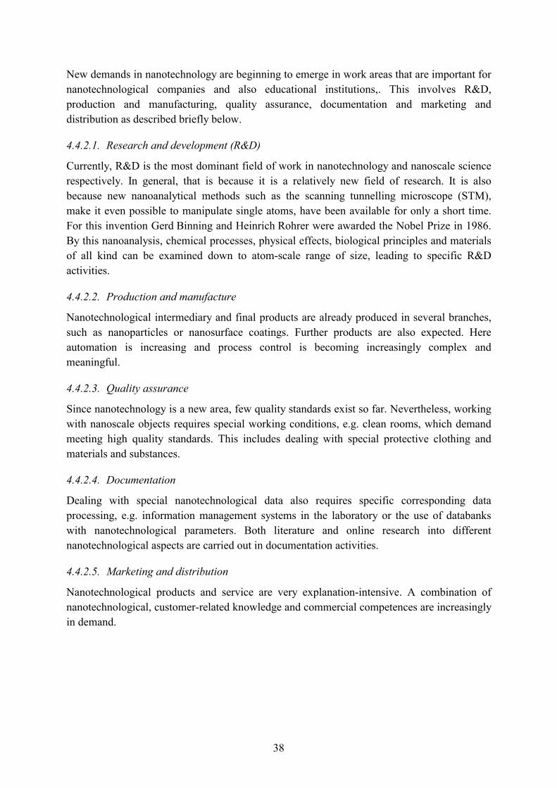
Table 8: Interdisciplinary fields of nanobiotechnology....................................................... 40
Table 9: Examples of professional competences in the field of nanochemistry.................. 40
Table 10: Procedures of nanobiotechnology ......................................................................... 41
Table 11: Soft skills............................................................................................................... 41
Table 12: Overview of qualification profiles......................................................................... 42
Table 13: Interdisciplinary qualification profile (16): specialist for nanosurface treatment................................................................................................................ 43
Table 14: Model of further education modules in nanotechnology....................................... 46
Figures
Figure 1: Classification of technology as a science .............................................................. 14
Figure 2: Phase structure of technological processes............................................................ 14
Figure 3: The cross sectional quality of nanotechnology...................................................... 17
Figure 4: Applications of nanoanalysis................................................................................. 18
Figure 5: Public funds for nanotechnology worldwide......................................................... 22
Figure 6: World market prognoses for nanotechnology ....................................................... 24
Figure 7: National and international nanotechnology networks in Europe by country of coordinator 2003 ............................................................................................... 27
Figure 8: Number of graduate courses and degrees on nanotechnology............................... 33
Figure 9: Which graduates are needed? ................................................................................ 34
Figure 10: Undergraduate degrees/courses in nanotechnology............................................... 35
Figure 11: Number of short courses in nanotechnology ......................................................... 36
Figure 12: Main hurdles in the development of nanotechnologies......................................... 36
Figure 13: Recruiting adequately qualified personnel ............................................................ 37

7
Executive summary Nanotechnology is set to play a key role worldwide in the 21st century. It is trend-setting across industrial areas where nanoscale and typical quantum mechanical phenomena are prevalent, bringing new functions and properties to improve or develop new products and application possibilities. Nanotechnology is a cross-sector technology which is increasingly relevant to economic areas such as chemistry, medical technology, automobile and the food industry. All current prognoses assume a dramatic increase in the economic significance of nanotechnology, making qualified staff an urgent precondition for the effectiveness of associated research and production.
In this context, the secondary analysis in this document presents the latest selective research, development tendencies and trends in the different fields and sectors of nanotechnology, and their related skill needs. The study is based on research results from Europe and competing industrial nations such as Japan and the US. It includes a definition of nanotechnology, with fields and sectors of its application, particularly in Europe. It reviews estimates and forecasts of the significance and scientific-technological developments of nanotechnology in various fields. The study analyses future demand for skills in the nanotechnology labour market, indicating major sources and institutions involved in investigating the future demand for appropriate qualifications. The analysis presents a review of research results on specific and basic skills, particularly of innovative skills required and emerging new occupations. Finally, it proposes ways of implementing and verifying Europe-wide innovative qualification and training measures.
Additionally, the study is based on previous research results on qualification requirements in nanotechnology in Germany (1).These results allow assessment of nanotechnology applications, typical fields of work at an intermediate qualification level (specialists) and expertise of institutions active in nanotechnology from the point of view of their relevance and transferability across Europe and beyond.
Primary and secondary data from available resources, mainly online, was assessed using a special systematisation instrument in the form of a matrix based on principles of ‘general technology’. Typical matrix parameters are technological processes, technical devices and systems. This approach allows examination of different manifestations of nanotechnology in technical systems and processes to identify related skill needs.
Trends in research and development (R&D) and related skill needs are presented for nanoanalysis, nanobiotechnology, nanochemistry, nanoelectronics and nanooptics. Applications of several nanotechnological developments are described for energy and environment, life science, medicine, pharmacy, cosmetics, chemistry, textile and food industry, information and communication technologies, automotive, household and sports equipment.
Nanotechnology is becoming increasingly significant worldwide, reflected not least in expenditure on support measures in industrial nations. Alarmingly, nanotechnology education is only supported by the EU, India and the US.
(1) The isw implemented between 2002 and 2005 a project regarding identification of skill developments in
nanotechnology in Germany.
8
As well as its assessment of several key research questions and application fields, the study presents a list of relevant initiatives, programmes and networks at national and international level.
Demand for qualified nanotechnology personnel is increasing in R&D. The development of new products and services also demands more well-trained staff in manufacturing, quality assurance, marketing and distribution. The study presents qualitative and quantitative information. For instance, in 2004 the European network Nanoforum conducted an online survey to assess responses to the European Commission’s proposed document Towards a European strategy for nanotechnology. Altogether 749 persons were questioned across Europe. In this context it is especially noticeable, that there is an urgent need to develop nanotechnology education and training, with 90 % of participants indicating that interdisciplinarity is considered to be crucial (Malsch and Oud, 2004).
As well as a review of existing education and training opportunities in Europe, the US and Asia, the study presents the results of qualitative research in Germany regarding the identification of trend-setting skills in nanotechnology. New skill requirements in companies were analysed and summarised within so-called qualification profiles for R&D, manufacturing, quality assurance, documentation of analyses, research and production processes, marketing and distribution.
Referring to the overall analysis of skill development in nanotechnology, the study proposes a six steps route to implementing and verifying innovative training measures in Europe. Following analysis of nanotechnology and its institutions in Europe and worldwide, a survey of scientific-technological development, identification of innovative demands for qualification and the development of qualification profiles, new training measures throughout Europe have to be developed and tested. The next step is the generalisation and broad implementation of new education and training measures.
The authors conclude, on the basis of international comparison, that there is extensive public promotion of sciences and technological research. Unfortunately few activities can be found regarding identification and development of the required human resources. As far as these activities are promoted, they are usually a component of science and technology research and lead to individual solutions without involving the neighbouring areas. In the medium-term this could cause a shortage of qualified employees, which could be a limiting factor for the successful transfer from nanotechnological research to nanotechnological production.
It is recommended to use a significant part of promotional funds (e.g. 5 %) to identify skill needs and to develop and test training, so preventing obstacles to economic utilisation of research results caused by a shortage of human resources. Risks of emergence of patchwork solutions are to be met by a systemic approach both for initial education and further education and training; a monitoring programme is urgently recommended to identify skill needs from qualitative and quantitative points of view. The results should be transferred into an action plan for education and training. Additionally, the European Social Fund (ESF) could be used for developing and testing practical training measures. Institutions for vocational education and training, centres of excellence and the exchange of best practice in the area of nanotechnology should be more strongly promoted in Europe.
9
1. Introduction
Nanotechnology (2) is set to play a key role worldwide in the 21st century. It is trend-setting in all industrial areas and is advancing through an ever-growing number of discoveries. Due to the nanoscale and the typical quantum mechanical phenomena prevalent in industry, new functions and properties are added to improve or develop new products and application possibilities. Nanotechnology is a cross-sector technology, which is increasingly relevant economic areas such as chemistry, medical technology, automobile and foodstuff industries. Current prognoses assume a dramatic increase in the economic significance of nanotechnology, making qualified staff an urgent precondition for the effectiveness of research and production.
The European Commission (EC, 2004a) calls upon Member States to contribute to:
(a) identifying educational demands on nanotechnology and providing examples of best practice or results of pilot studies;
(b) encouraging the definition and implementation of new courses and curricula, teacher training and educational material for promoting interdisciplinary approaches to nanotechnology, both at school and graduate level;
(c) integrating complementary skills into post-graduate and lifelong training, e.g. entrepreneurship, health and safety issues at work, patented inventions, ‘spin-off’ mechanisms, communication, etc.
In this context the study will demonstrate new demands for qualification in nanotechnology and the need to improve training and higher education. Introducing nanotechnological qualification contents into professional and vocational training will be decisive in maximising nanotechnology’s potential. Companies with nanotechnological business activities need an increasing number of qualified staff. Even though the economic significance of nanotechnology is increasing, many applications are currently at the level of research or applied R&D, with numerous trends and development tendencies having growth potential but not being seen as sufficiently concrete. Due to nanotechnology’s enormous innovation potential, R&D jobs are mainly carried out by higher education at present indicating an increasing need for graduates. In addition, further achievements in intermediate skill needs are necessary, i.e. vocational training, to process research results in nanotechnological production. Investigation into demands at qualification intermediate level plays an important role in this secondary analysis. To be able to fill the demand for adequately qualified staff in the relevant nanotechnology fields of work, exploration into innovative job and qualification requirements is necessary.
This analysis contains a review of research into the demand for qualification and skills in nanotechnology.
(2) Nanotechnology is the production, examination and application of structures, molecular material and inner
border areas and surfaces with at least one critical dimension or production tolerance under 100 nm (nanometers) (Bachmann, 1998).
10
2. Research objectives
The overview is drafted on the basis of available research results in Europe and in other competing economies such as Japan and the US.
Key points of the research have been the following:
(a) definition of nanotechnology, its fields and sectors of its application and implementation, particularly in Europe.
The range of application and implementation of nanotechnology is rather broad. Nanotechnological products are used worldwide to solve many problems, e.g. in medical technology (new cancer fighting methods), electronics (larger data storage capacity) and in promoting new energy supply (more efficient solar technology). To carry out a review of technological processes and products, a specific systematisation instrument was needed;
(b) review of estimates and forecasts of significance and scientific-technological developments of nanotechnology in various fields.
The economic potential of nanotechnology is very differently assessed around the world. All current prognoses assume a dramatically increasing economic significance of nanotechnology. It was necessary to provide significant estimates and forecasts to review them;
(c) future demand in the nanotechnology labour market.
A growing number of companies develops and manufactures nanotechnological products in cooperation with research institutes. Companies with such nanotechnological business activities need more skilled staff, so it was necessary to assess the development of the nanotechnology labour market;
(d) identification of and the main bodies involved in investigating future qualification demands for nanotechnology.
This required reviews of relevant actors in nanotechnology, such as companies, scientific institutions, networks and competence centres;

11
(e) review of research results on specific and basic skills and particularly the innovative skills required and new occupations emerging in nanotechnology;
Fast changes in nanotechnology in science, engineering and technology require dynamic qualification development for employees. The early identification of basic qualifications and new/innovative qualifications was the object of the isw project Investigation into trend-setting qualification in the nanotechnology sector (3) in which, relevant research results have already been assessed. For a current overview, new relevant research results were identified and assessed;
(f) propose ways of implementing and verifying Europe-wide innovative qualification and training measures in nanotechnology.
Well-defined qualification requirements are the starting point for developing innovative qualification measures. Proposals on qualification and training contents have been developed to modify existing qualifications or to create new education and training programmes, e.g. a modular system. The proposals are based on Europe-wide implementation of education and training.
(3) The fields nanooptic, nanomaterial, nanoanalysis, nanobiotechnology and nanoelectrics have been analysed
to identify new/innovative qualification developments in Germany. Additional general/basic skill requirements have been identified during the research process.
12
3. Methodological approach
The analysis is based on research by the isw on qualification requirements in nanotechnology in Germany (4). A number of research results have been assessed for relevance and transferability for European and international contexts:
(a) nanotechnology links to implementation and application;
(b) typical fields of work at an intermediate qualification level (specialists);
(c) expertise of active institutions in nanotechnology;
This procedure allowed the definition of guidelines for secondary analysis to answer the key points and questions of the research.
In addition, nanotechnology networks and competence centres were contacted to make sure that relevant literature and data were analysed. In some European cases it was necessary to conduct telephone-based research with experts and active institutions to analyse further data and relevant expertise so guidelines for questioning respondents were developed.
3.1. Secondary analysis
Secondary analysis is an analysis of data collected by primary researchers for another aim or within another context. The analysis of available research on demands for qualification and skills in nanotechnology generated a compilation of research results as well as a review of actual skill needs. Sources for the secondary analysis were found on the Internet, in data banks and libraries. In addition, isw project results on early identification of trend-setting skills in nanotechnology were used. Apart from the regular analysis of economic data, trends and statistics it was necessary to arrange the huge technology-based data set. Therefore, a new instrument was used to systematise different technology-oriented information. The matrix, based on the principles of ‘general technology’, helped to systemise data using the parameters of technological processes, technical devices and systems, and skill demands. This instrument allows evaluation of both primary and secondary data, especially in nanotechnology.
(4) isw project to identify trend-setting skills in the nanotechnology sector in Germany, project title Ermittlung
von Trendqualifikationen im Bereich der Nanotechnologie, project homepage: www.isw-institut.de/nano.
13
3.2. The systematisation matrix
The matrix was developed to create an instrument for systemising and analysing the different manifestations of nanotechnology, as there are technical systems, processes, principles and effects, systematically towards trend-setting qualifications (5). When there are new or changed technical systems or technological processes within the field of activity of qualified staff, their skills and competences are developed. Changes in use of material require different skills. Against this background, technological processes proved to be the most meaningful ordinal criterion of the different manifestations, hence they became the preamble of the matrix, which soon proved to be a systematic matter of study. The development of the systematisation matrix is documented in detail in a special methodical paper (Abicht et al., 2003a).
Technological processes from nanotechnology are rarely systematically analysed like other technological fields (Grupp, 1995).
Because no systematic registration of nanotechnological processes could be found to allow conclusions about current skills, an instrument to systematise technological processes that takes technology as a science into account, which records the logical level of manifestation and which reveals the connections, has been worked out by the isw. With the help of a first search it should be clarified:
(a) whether announcements are relevant for the qualification research;
(b) which terms (product, production process, technical system) the observation of technological appearance is related to;
(c) if there is any complementary information to be found in other fields after the classification.
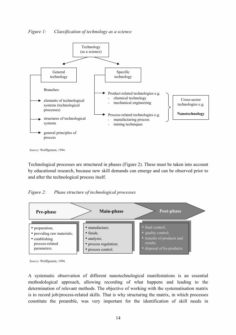
Technology as a science is an important basis for systemising, with specific characteristics of technologies differentiated and examined. Nanotechnology, due to its interdisciplinary character, contains product-related as well as process-related technologies (Figure 1).
(5) The isw project Ermittlung von Trendqualifikationen im Bereich der Nanotechnologie (Identification of
trend–setting skills in the nanotechnology sector) developed a new instrument to systemise different technology-oriented information.
14
Source: Wolffgramm, 1994.
general principles of process
General technology
Branches:
elements of technological systems (technological processes)
structures of technological systems
Specific technology
Product-related technologies e.g. - chemical technology - mechanical engineering
Process-related technologies e.g. - manufacturing process - mining techniques
Technology (as a science)
Cross-sector technologies e.g.
Nanotechnology
Phasenstruktur technologischer VerfahrenPre-phase Main-phase Post-phase
• manufacture; • finish; • analysis; • process regulation; • process control.
• preparation; • providing raw materials; • establishing
process-related parameters.
• final control; • quality control; • transfer of products and
results; • disposal of by-products.
Source: Wolffgramm, 1994.
Figure 1: Classification of technology as a science
Technological processes are structured in phases (Figure 2). These must be taken into account by educational research, because new skill demands can emerge and can be observed prior to and after the technological process itself.
Figure 2: Phase structure of technological processes
A systematic observation of different nanotechnological manifestations is an essential methodological approach, allowing recording of what happens and leading to the determination of relevant methods. The objective of working with the systematisation matrix is to record job/process-related skills. That is why structuring the matrix, in which processes constitute the preamble, was very important for the identification of skill needs in
15
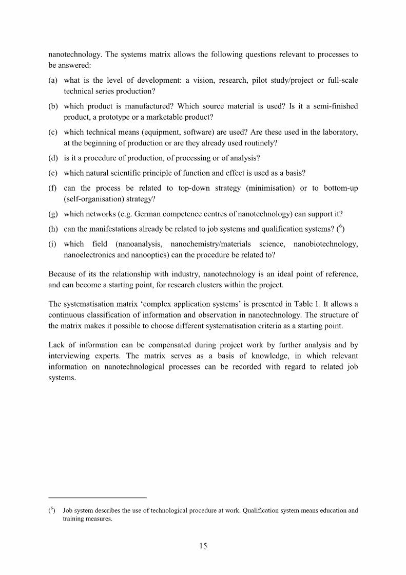
nanotechnology. The systems matrix allows the following questions relevant to processes to be answered:
(a) what is the level of development: a vision, research, pilot study/project or full-scale technical series production?
(b) which product is manufactured? Which source material is used? Is it a semi-finished product, a prototype or a marketable product?
(c) which technical means (equipment, software) are used? Are these used in the laboratory, at the beginning of production or are they already used routinely?
(d) is it a procedure of production, of processing or of analysis?
(e) which natural scientific principle of function and effect is used as a basis?
(f) can the process be related to top-down strategy (minimisation) or to bottom-up (self-organisation) strategy?
(g) which networks (e.g. German competence centres of nanotechnology) can support it?
(h) can the manifestations already be related to job systems and qualification systems? (6)
(i) which field (nanoanalysis, nanochemistry/materials science, nanobiotechnology, nanoelectronics and nanooptics) can the procedure be related to?
Because of its the relationship with industry, nanotechnology is an ideal point of reference, and can become a starting point, for research clusters within the project.
The systematisation matrix ‘complex application systems’ is presented in Table 1. It allows a continuous classification of information and observation in nanotechnology. The structure of the matrix makes it possible to choose different systematisation criteria as a starting point.
Lack of information can be compensated during project work by further analysis and by interviewing experts. The matrix serves as a basis of knowledge, in which relevant information on nanotechnological processes can be recorded with regard to related job systems.
(6) Job system describes the use of technological procedure at work. Qualification system means education and
training measures.
16
Source: Abicht et al., 2003a.
Sol-gel-procedure
x
x
x
x
x
x
Metal alcoholate, Si-Alcoxidesa.o.,
percipitating agent
(ceramics) nanoparticles, fibres,
coatings, aerogels (porous gels)
Sol-gel-reactors
Reaction rate (relation rate of
formation/growth rate), quantity
and sort of basic materials,
temperature, pH
Wet - chemical reaction
1. Sol production, basic materials got
hydrolised, means brought into solution;
2. by condensation of the sol a
reorganisation of the solutes to a gel
takes place (polymerisation).
Rössler et al. (2001)
CVD - chemical
vapor deposition
x
x
x
x
x
x
Products or educts of chem. Vapor
synthesis, e.g. titanium oxide
Nanoparticles, coatings, films
Hot-wall and cold-wall reactors, low-
pressure flame reactors, plasma
reactors, laser reactors
Temperature, reaction rate
(relation coagulating rate/
growth rate) pressure,
composition of basic materials
chemical reaction
By means of the CVD gaseous
reactants are put on a substrate
surface as solid coating by chemical
reactions.
Unrecht (2001)
CVS - chemical
vapor sythesis
x
x
x
x
x
?
Precursor: Gas (TiCl4,
SiCl4, Fe(CO)5, Si2O(CH3)6)
Nanoparticles of (metal)-oxids
e.g. TiO2, SiO2, Fe3O4, soot, silicate
Low-pressure flame reactors, hot-wall
reactors, plasma reactors, laser
reactors Sputtering-procedure
Temperature, reaction rate
(relation coagulating rate/
growth rate) pressure,
composition of basic materials
chemical reaction
The precursors corrode in a reactor
by the supply of high temperature.
Either the products got steady
synthesised by the chem. reaction or
the supersaturate Precursor gas
quickly cools down
Rössler et al. (2001)
Producing
Processing
Apply
Measure/
control
Nanoelektronics
Nanooptics
Nanochemistry
Nanobiotech.
Nanoanalysis
Nano-materials
Nanoclub Lateral
NanOp
Ultra-thin funct. Coat.
NanoChem
Ultra-precise Surf.
Nano-analysis
Nanomat
Nano.bionet
not available
available
observable
not available
available
observable
Initial
condition
Final
condition
Area of
procedure
Process of change
(technology)
Strategy
Top-down Bottom-up
Nanobranches
Centre of
competence
Job system
Sytem of
qualification
Source
Product
System of change
(technical means)
Parameter/control
Natural scientific
principle
Description
Table 1: The systematisation matrix ‘complex application systems’ (extract)
17
Nanotechnology
Pharmacy Textile industryAutomobile
industry
Medical technology
Biotechnology
Chemical industry
Environmental technology
Food industry
Source: isw figure
4. Results In this chapter the following topics are presented: nanotechnology fields and sectors; international potential, trends and developments; future demand for qualified staff/development of the labour market, skill needs in nanotechnology; institutions to work on early identification of skill needs. In addition, ways of implementing and verifying innovative qualification and training measures across Europe are detailed.
4.1. Nanotechnology sectors
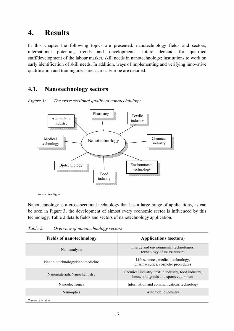
Figure 3: The cross sectional quality of nanotechnology
Nanotechnology is a cross-sectional technology that has a large range of applications, as can be seen in Figure 3; the development of almost every economic sector is influenced by this technology. Table 2 details fields and sectors of nanotechnology application.
Table 2: Overview of nanotechnology sectors
Fields of nanotechnology Applications (sectors)
Nanoanalysis Energy and environmental technologies, technology of measurement
Nanobiotechnology/Nanomedicine Life sciences, medical technology, pharmaceutics, cosmetic procedures
Nanomaterials/Nanochemistry Chemical industry, textile industry, food industry, household goods and sports equipment
Nanoelectronics Information and communications technology
Nanooptics Automobile industry
Source: isw table
18
Innovative interdisciplinary
skill needs
Nano-analysis
Nanochemistry
Nanobiotechnology
Nanooptics
Nanoelectronics
Source: isw figure
4.1.1. Fields of nanotechnology
4.1.1.1. Nanoanalysis
Nanoanalysis refers to special techniques for determining the atomic structures of materials. It is a cross-sectoral discipline which supplies analytic methods and means for recording basic phenomena and for characterising products and, further, results in analytical quality assurance by making a contribution to national and international standardisation. Nanoanalytical techniques offer many possibilities to make scientific information available to physics, chemistry, biology, materials science and engineering on a nanometer scale. Steady miniaturisation requires understanding and control of processes on the nanoscale.
Nanoanalysis and the process of analysis and measuring devices make it possible to do specific surveys and manipulation in the nanocosmos. Therefore, it is of crucial importance to nanotechnology.
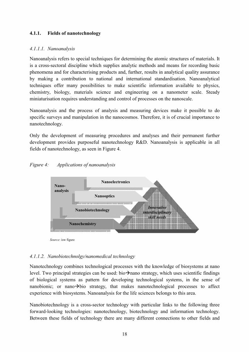
Only the development of measuring procedures and analyses and their permanent further development provides purposeful nanotechnology R&D. Nanoanalysis is applicable in all fields of nanotechnology, as seen in Figure 4.
Figure 4: Applications of nanoanalysis
4.1.1.2. Nanobiotechnolgy/nanomedical technology
Nanotechnology combines technological processes with the knowledge of biosystems at nano level. Two principal strategies can be used: bio nano strategy, which uses scientific findings of biological systems as pattern for developing technological systems, in the sense of nanobionic; or nano bio strategy, that makes nanotechnological processes to affect experience with biosystems. Nanoanalysis for the life sciences belongs to this area.
Nanobiotechnology is a cross-sector technology with particular links to the following three forward-looking technologies: nanotechnology, biotechnology and information technology. Between these fields of technology there are many different connections to other fields and
19
branches, e.g. molecular simulation, nanomedicine or biological computer science. Further, nanobiotechnology offers high innovation potential for the food industry, agriculture and ecology. Some important natural scientific fields linked with nanobiotechnology are molecular biology, genetics, colloid chemistry, biochemistry, surface physics and quantum mechanics. From the technical point of view, engineering is significant to developing and implementing nanobiotechnological products, systems, processes and methods. In particular, the medical and pharmaceutical branches of diagnostics and therapeutics, with their different R&D fields, occupy an important part of nanobiotechnology.
4.1.1.3. Nanomaterials/nanochemistry
There are different views worldwide on what exactly can be assigned to the field of nanochemistry, which deals with creating and manipulating nanoactive chemical systems. Supramolecular functional systems are the basic principles for forming new materials. Nanochemistry – which is not internationally standardised – means chemical changes in systems, which work exclusively on the nanoscale. Nanochemistry specifically includes functional supramolecular systems, e.g. transport of active agents, systems that can be switched or controlled, systems with adjustable characteristics, functional coatings and the formation processes of nanoparticles (particles, colloids, fluids, nanotube) (7). Müller and Righi (2002) believe it is possible that the paradigm in materials’ science is being changed by nanotechnology; away from a top-down method of adapting materials step by step for new demands to the bottom-up construction of materials atom by atom to obtain the desired characteristics.
4.1.1.4. Nanoelectronics
The field of nanoelectronics is not strictly defined because the transition from microelectronics to nanoelectronics is fluid. Currently, microelectronics deals in the realm of up to 90 nm (nanometers). Integrated circuits (significantly) below the 100 nm scale are called nanoelectronics. It is reckoned on a further miniaturisation (top-down approach) down to 23 nm (10-9 m) within the next decade. Optical lithography reaches its limits for physical laws (wavelength), so that a change in technology can be expected in the near future.
4.1.1.5. Nanooptics
Nanooptics includes the research, development and production of optical components, structures and systems on the nanometer scale. Nanooptics deals with several branches such as ultraprecision optics that manufactures nanometer precise lenses and lens systems used in appliance optics and medical optics. Laser technology, which is used for optoelectronical components in information and communication technology, is another important branch.
(7) VDI, Bachmann 2002.
20
In optics or photonics, nanotechnological aspects are important in different areas. Photonics deals with technologies for production and application of light and other radiant energies, based on photons. The range of application of photonics is wide and diverse; it extends over energy production, detectors, telecommunications and informatics.
4.1.1.6. Applications of nanotechnology
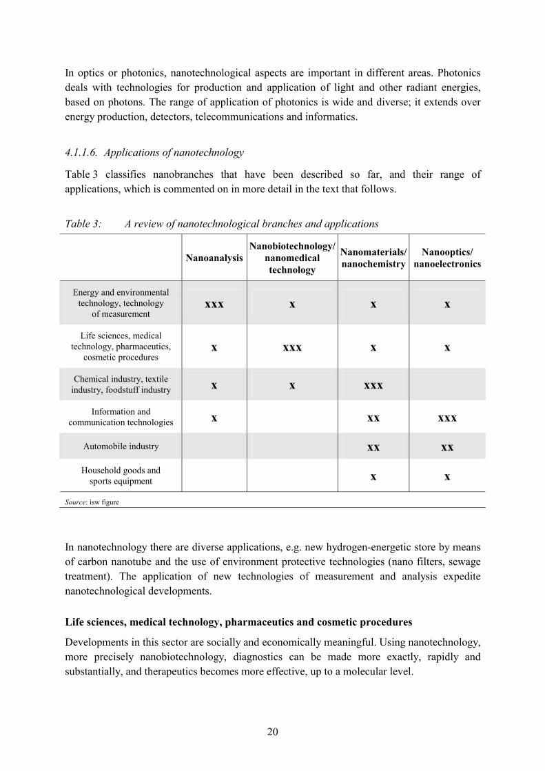
Table 3 classifies nanobranches that have been described so far, and their range of applications, which is commented on in more detail in the text that follows.
Table 3: A review of nanotechnological branches and applications
NanoanalysisNanobiotechnology/
nanomedical technology
Nanomaterials/ nanochemistry
Nanooptics/ nanoelectronics
Energy and environmental technology, technology
of measurement xxx x x x
Life sciences, medical technology, pharmaceutics,
cosmetic procedures x xxx x x
Chemical industry, textile industry, foodstuff industry x x xxx
Information and communication technologies x xx xxx
Automobile industry xx xx
Household goods and sports equipment x x
Source: isw figure
In nanotechnology there are diverse applications, e.g. new hydrogen-energetic store by means of carbon nanotube and the use of environment protective technologies (nano filters, sewage treatment). The application of new technologies of measurement and analysis expedite nanotechnological developments.
Life sciences, medical technology, pharmaceutics and cosmetic procedures
Developments in this sector are socially and economically meaningful. Using nanotechnology, more precisely nanobiotechnology, diagnostics can be made more exactly, rapidly and substantially, and therapeutics becomes more effective, up to a molecular level.
21
Chemical industry, textile industry, foodstuff industry
Chemical application is the basis for many diverse developments. Surfaces coated with nanoparticles, functional coatings, composition of different materials and structures lead to totally new characteristics. At present this is a growing sector. The development of specific sensors (freshness, tracing back, etc.) functional packaging and additives are fields of application in food industry.
Information and telecommunication technologies
Information technology and telecommunications are among those fields with high growth rates expected within coming years. Labelling products with RFID (radio frequency identification) makes applications possible in many industrial branches and trades that are hardly imaginable. Innovative lithography and manufacturing processes lead to new generations of processors and non-volatile memory chips. Development and application of organic light-emitting diodes (OLED) lead to new ranges of application and communication. Intelligent textiles, with electronic components and coatings on the nanoscale, make applications of mobile information and communication technologies possible.
Automotive industry
Nanotechnology in this sector has potential for growth. It contributes to making vehicles safer, more environment- and user-friendly, and energy-saving. Nanotechnological developments promote the reduction of wear and tear of tyres and motors. New paints make automobiles safer from environmental influences and damage.
Household goods and sports equipment
Nanotechnology made its entrance in this sector as well. There are already cleaning agents on the market that, using components on nanoscale, make new effects in maintenance possible. Nanotechnology can also be found in sports equipment with, for example, tennis rackets reinforced by nanotubes or skiwaxes with nanoparticles.
22
Estimated government nanotechnology R&D investments worldwide
0
200
400
600
800
1000
1200
USD Mio
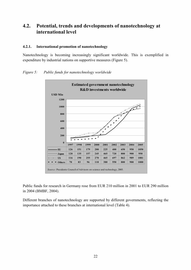
EU 126 151 179 200 225 400 650 950 1050
Japan 120 135 157 245 465 720 800 900 950
US 116 190 255 270 465 697 862 989 1081
Others 70 83 96 110 380 550 800 900 1000
1997 1998 1999 2000 2001 2002 2003 2004 2005
Source : Presidents Council of Advisors on science and technology, 2005.
4.2. Potential, trends and developments of nanotechnology at international level
4.2.1. International promotion of nanotechnology
Nanotechnology is becoming increasingly significant worldwide. This is exemplified in expenditure by industrial nations on supportive measures (Figure 5).
Figure 5: Public funds for nanotechnology worldwide
Public funds for research in Germany rose from EUR 210 million in 2001 to EUR 290 million in 2004 (BMBF, 2004).
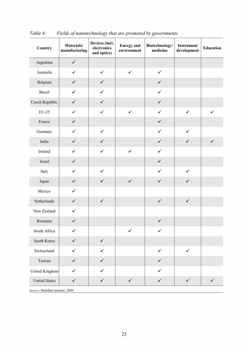
Different branches of nanotechnology are supported by different governments, reflecting the importance attached to these branches at international level (Table 4).
23
Table 4: Fields of nanotechnology that are promoted by governments
Country Materials/ manufacturing
Devices (incl. electronics and optics)
Energy and environment
Biotechnology/ medicine
Instrument development Education
Argentina
Australia
Belgium
Brazil
Czech Republic
EU-25
France
Germany
India
Ireland
Israel
Italy
Japan
Mexico
Netherlands
New Zealand
Romania
South Africa
South Korea
Switzerland
Taiwan
United Kingdom
United States
Source: Meridian Institute, 2004.
24
Different prognoses for world market potentials of nanotechnology
0
200
400
600
800
1000
1200
2005 2008 2010 2015
in bn EUR resp. in bn USD
Mitsubishi Research InstituteDG-BankSal. OppenheimNSFEvolution CapitalNanoBusinessAlliance
Source : isw figure according to various sources, 2002 (see legend).
It is clear that branch materials/manufacturing in particular has priority in public funding, because it is supported by all nations. Next in importance are biotechnology/medicine and devices (including electronics and optics).
Alarmingly, nanotechnology education is only supported by the EU, India and the US.
It should be noted that the data in the table refer to a questionnaire survey conducted in the framework of an international conference and thus may not be complete (Meridian Institute, 2004).
4.2.2. Economical significance of nanotechnology
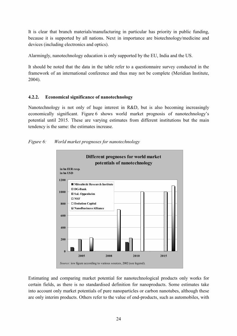
Nanotechnology is not only of huge interest in R&D, but is also becoming increasingly economically significant. Figure 6 shows world market prognosis of nanotechnology’s potential until 2015. These are varying estimates from different institutions but the main tendency is the same: the estimates increase.
Figure 6: World market prognoses for nanotechnology
Estimating and comparing market potential for nanotechnological products only works for certain fields, as there is no standardised definition for nanoproducts. Some estimates take into account only market potentials of pure nanoparticles or carbon nanotubes, although these are only interim products. Others refer to the value of end-products, such as automobiles, with
25
single components based on nanotechnology (e.g. the paints). As a result there are significant differences among these estimates.
While Europe has a leading position in chemistry and medicine/pharmacy, the US are leading in nanostructuring, and Asia in the field of nanoelectronics.
Europe and the US are producing good results in the field of nanostructured materials.
4.2.3. Selected research in nanotechnology
The following text presents some selected research trends in nanotechnology branches and applications (for detailed information see Annex 1):
(a) Nanoanalysis
There is a R&D trend of full-scale analysis instruments and more effective mass analyses (e.g. in the research of active agents to high throughput screening) and of highly specialised analytical instruments with a rather small range of application. The combination of different methods of proof in an analysis system is increasingly important, because they can measure several qualitative and/or quantitative parameters of a sample parallel, almost at the same time. The use of different methods of measurement – on optical, optoelectronical or a mechanical basis, or the basis of (bio)chemical-physical interrelation and biohybridised principles – is possible.
(b) Life sciences, nanomedical technology/nanobiotechnology/cosmetics
Innovative methods of analysis and diagnosis have been developed. They allow faster and lower-cost test methods with a small number of samples.
Personalised medicines, e.g. specific drugs for the individual’s need, innovative drugs and therapies, have been developed. Tissue engineering for therapies of damaged tissue or biometric and bio-compatible materials allow therapies that fit exactly for teeth, bone and cartilage tissue in the sense of a regenerative medicine. Another research key point is the development of functional nanoparticles that are used as carriers for drugs or other substances and that can clearly improve not only their addressing, transport and measuring out but also their effectiveness.
For cosmetic products, suntan lotions with high protection factors have been developed by using nanoparticles of titanium and zinc oxide as additives. In addition, skin creams with special lipoid acid, toothpaste, lipsticks or anti-microbial coatings and sprays have been developed.
(c) Chemical industry, nanomaterials/nanochemistry
A key point for R&D is the production of nanoparticles and the combination of different materials and structures that provide new characteristics. Examples are functional ultra-thin surface coatings, catalysts, enzymes, cleaning agents or dirt-resistant surfaces.
26
(d) Nanotechnology in the textile industry
For nanotechnology in the textile industry, research focuses on nanosurface coatings of textiles, e.g. with deodorant substances, smart clothes, such as intelligent textile provided with sensors taking one’s pulse or instruments for communication, or even the integration of active agents capsules in textiles (e.g. with vitamin C).
(e) Nanotechnology in the food industry
Research key points for the use of nanotechnology in the food industry are functional packing for food, additives or sensors to measure freshness, deep-frozen throughout.
(f) Electrics/electronics, nanoelectronics, information and communication technologies
R&D trends are innovative methods of lithography to produce more efficient electronics that make, for example, restarts of computers unnecessary. Innovative micro- or nanoelectronic-mechanical systems provide new sensors and actuators in car manufacture. In addition, a particular technology provides more data communications by using specific labels on all products. This helps to improve logistics.
(g) Optical industry, nanooptics
Development and production of highly precise optical elements such as lenses, mirrors and crystals provides modern outstanding performing optics as well as ultra precision optics. Laser techniques and laser optimised by nanotechnology become increasingly brilliant and less energy-intensive, therefore they have a wider range of application, e.g. lighting installation in vehicles. They provide new energy-saving and mechanically flexible displays that are already used for digital cameras (Kodak). New optical memory mediums using blue laser offer vast data capacity and are going to replace DVD techniques.
(h) Automotive industry
Key points of R&D in automotive are effective catalysts, soot particles filters, scratch-proof paints (Daimler-Chrysler) as well as surface coating.
4.2.4. National activities, initiatives, programmes and networks
As well as the study of selected research and applications of nanotechnology, currently several national activities, initiatives, programmes and networks referring to nanotechnology at international and national level are established. Therefore, there can be no assumption that all activities are covered
4.2.4.1. Nanotechnology across Europe (a) Under the Sixth Framework Programme (FP6) of the EU there is a specific programme
devoted to nanotechnology materials and production processes with funds of EUR 1 429 billion.
27
National and international nanotechnology networks by country of coordinator 2003
0
2
4
6
8
10
12
14
16
18
EC AT BE CH CZ DE DK ES FI FR GR HU IE IT LT LU NL PL PT RO SE SI SK UK
Number of networks
national
international
Source : Folea, 2003.
(b) Nanoforum is a European nanotechnology network, which was founded by the Fifth Framework Programme (FP5) of the EU to provide information on European nanotechnology efforts and to support the European nanotechnology community.
(c) European Nanoelectronic Initiative Advisory Council (ENIAC) - a European initiative to strengthen nanoelectronics.
(d) European NanoBusiness Association (ENA) founded in 2002:
(i) members from venture capital;
(ii) representing the whole spectrum of nanobusiness;
(iii) addresses global and local issues from standards for education and legislation.
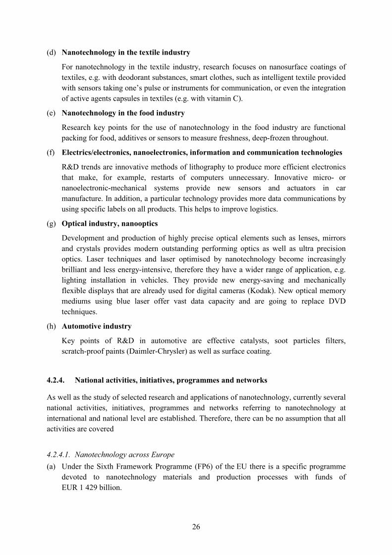
In research-intensive technology sectors, networks of research institutes, enterprises and other institutions provide promising models, allowing the know-how of different groups to be shared. There are already several networks at national and international level which have been set up across Europe, as seen in Figure 7.
Figure 7: National and international nanotechnology networks in Europe by country of coordinator 2003
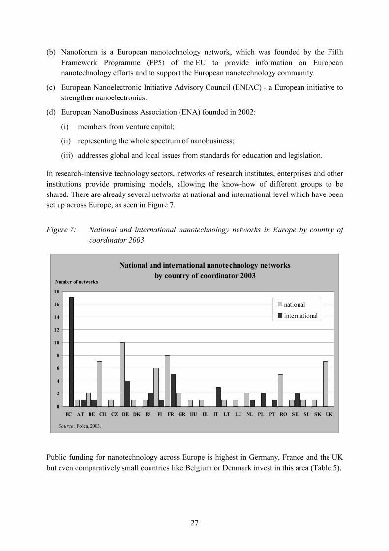
Public funding for nanotechnology across Europe is highest in Germany, France and the UK but even comparatively small countries like Belgium or Denmark invest in this area (Table 5).
28
Table 5: Estimates of public funds for nanoscale science and nanotechnology
EUR Mio
Country 1997 1998 1999 2000
Belgium 0.9 1 1,1 1.2
Denmark 3 1.9 2 2
Germany 47 49 58 63
Greece 0.2 0.2 0.3 0.4
Spain 0.3 0.3 0.4 0.4
France 10 12 18 19
Ireland 0.4 0.4 0.5 3.5
Italy 1.7 2.6 4.4 6.3
Netherlands 4.3 4.7 6.2 6.9
Austria 1.9 2 2.2 2.5
Portugal 0.2 0.2 0.3 0.4
Finland 2.5 4.1 3.7 4.6
Sweden 2.2 3.4 5.6 5.8
United Kingdom 32 32 35 39
Source: Ilfrich and Kunert, 2005.
Austria Austrian nano initiative is supported by the BMVIT, Federal Ministry for Transport,
Innovation and Technology;
Austrian nano forum is a part of this initiative; the forum approves the national programme for nanotechnology.
France From 2005, and for the following three years, the French government increased
expenditure on research to EUR 70 million, with primary focus on nanotechnology;
Laboratory of Electronics and Information Technologies (LETI) deals with nanotechnology among others.
Germany Nine competence centres (CCs) supported by the Bundesministerium für Bildung und
Forschung (BMBF) which focus on different nanotechnological themes, CC Nanochem, CC NanOP, CC NanoBioNet, CC NanoMat, etc.;
29
BMBF campaign ‘nanoTruck’ with own vehicles for display purposes throughout Germany;
about 450 enterprises referring to nanotechnology in Germany (Luther et al., 2004);
Fraunhofer Centre for Nanoelectronic Technologies (CNT) in Dresden;
CeNTech Centre for Nanotechnology in Minster.
Switzerland
The initiative Top Nano 21 is a programme focused on technology and addressed to representatives of science and industry.
United Kingdom National Micro- and Nanotechnology (MNT) initiative of the UK government;
the Institute of Nanotechnology deals exclusively with nanotechnological themes.
4.2.4.2. Worldwide
International workshops and conferences are organised by the Global Nanotechnology Network (GNN).
The leading countries in nanotechnology worldwide are the US, Japan, China and Germany (8).
United States National Nanotechnology Initiative (NNI), multi-agency, multi-disciplinary programme
supporting all aspects of nanoscale science, engineering and technology;
Nanoscale science, engineering and technology (NSET);
National Centre for Learning and Teaching (NCLT) in nanoscale size and engineering;
Nano education programmes:
- research experience for undergraduates (REU);
- materials research internships for minority undergraduates (MRI);
- research experience for science teachers (REST);
- materials world modules programme (MWM);
- nanoscience and technology programmes in colleges and universities;
- nanoscale science and engineering education (NSEE);
(8) Helmut Kaiser Consultancy 2003, www.hkc22.com/nanochina.html.
30
Sematech consortium on development of technology, joined by: Advanced Micro Devices (AMD), Freescale, Hewlett-Packard, International Business Machines (IBM), Infineon, Intel, Panasonic, Philips, Samsung, Spansion, Taiwan Semiconductor Manufacturing Company (TSMC), Texas Instruments;
Dakota County Technical College (DCTC) featuring a formal nanoscience technician programme. The college received a USD 900 000 grant from the National Science Foundation (NSF) in 2004 to begin the programme in partnership with the University of Minnesota. Cost is USD 200, however all participants will receive a USD 250 grant, sponsored by the NSF;
Chippewa Valley Technical College has teamed up with UW-Eau Claire, UW-Stout and several other technical colleges to create the first national nanoscience technology degree programme.
4.2.4.3. Asia
Asia nano forum (ANF) includes 13 member states: Australia, China, Hong Kong, India, Indonesia, Japan, Malaysia, New Zealand, Singapore, South Korea, Taiwan, Thailand and Vietnam.
Japan
The (Nano)Electronic initiative Selete (Semiconductor Leading Edge Technologies, Inc.) (www.selete.co.jp) was founded in 1996, with a staff of 250 employees and the following shareholders: Fujitsu Ltd; Matsushita Electric Industrial Co., Ltd; NEC Electronics Corporation; Oki Electric Industry Co., Ltd; Renesas Technology Corporation; Rohm Co., Ltd; Sanyo Electric Co., Ltd; Seiko Epson Corporation; Sharp Corporation; Sony Corporation; Toshiba Corporation.
China more than 600 companies deal with nanotechnology (9);
sub-themes:
- nanomaterials and preparation; - self-assembly technology; - nanoelectronics devices and nanophotonics devices; - micro-electronic-mechanical systems (MEMS) and nano-electronic-mechanical systems
(NEMS); - nanobiotechnology; - nanomedicine;
(9) Helmut Kaiser Consultancy 2003, www.hkc22.com/nanochina.html.
31
- characterisation and measurement of nanostructure; - computation and modelling at nanoscale; - consumer nanotechnologies and applications;
60 universities offer courses on nanoscale science and nanotechnology;
general education programme for undergraduates;
postgraduate advanced programme (80 hours course).
Taiwan
The Taiwan government started a six-year national programme on nanoscience and nanotechnology in 2003, which is supported by the public funds of seven different departments to promote R&D in this sector. The total budget is more than USD 600 million.
4.3. Labour market developments and future demand for qualified staff
With the focus on nanotechnology research comes an increasing demand for qualified staff. With the development of new products and services, the demand for well trained staff in industrial fields of work, such as production, quality assurance and in marketing and distribution will also increase.
Quantitative statements on the development of personnel demand already exist. Therefore, the European network Nanoforum conducted in 2004 an online survey to assess responses to the European Commission’s proposed document Towards a European strategy for nanotechnology (Malsch and Oud, 2004). Altogether 749 people responded. A total of 720 people participated via an online questionnaire and 29 wrote directly. Of those questioned 93 % came from 32 European countries. Thus, this opinion poll is one of most extensive across Europe. In addition to representatives from R&D, opinions were also sought from journalists, lecturers and representatives from commerce and industry. Among other results the survey came up with the following findings:
(a) nanotechnology will exert a strong impact on European industry (90 % agreement) and European citizens (80 %) within 10 years;
(b) Europe’s position is behind the US in nanoscale science (76 %) as well as in transferring nanotechnologies to industries (77 %);
(c) the influence of nanotechnology is particularly foreseen in the branches of chemistry and materials, information an telecommunication technologies, health service and security/defence;
(d) European public funds supporting nanotechnology should be increased significantly (79 %);
32
(e) 64 % support setting up new institutions at European level, e.g. in nanomedicine, nanomaterials and information technologies, to meet the demand for a suitable European infrastructure;
(f) human resources is a priority, participants expect a shortage of skilled personnel for nanotechnology within ten years (almost 50 %) or even within five years (25 %);
(g) there is an urgent need to develop nanotechnology education and training with 90 % of participants indicating that interdisciplinarity is crucial;
(h) aspects of health service, security and pollution should be taken into account early by research (75 %), therefore a matter of priority should be bridging the gaps in the knowledge about free nanoparticles (72 %);
(i) Europe should monitor the effects of nanotechnology on society (75 %) so more dialogue is needed;
(j) cooperation with developed (96 %) and less developed (76 %) countries is important and an international code of conduct would be welcome (87 %).
In this context it is particularly remarkable, that about 75 % of those questioned already expect a lack of qualified and interdisciplinary trained personnel within five to ten years. This makes clear how important it is to prepare early for new demands for qualification and training in nanotechnology. These estimates are confirmed by the recently published study by the VDI Technologiezentrum (Luther et al., 2004), stating that an increase in employment of 10 000 to 15 000 jobs in nanotechnology is expected throughout Germany within 2006.
According to the Business Communication Company (Edwards, 2003), worldwide manpower in nanobiotechnology alone by the year 2015 is estimated at around 160 000. It can thus be assumed that there is a growing need of manpower worldwide in nanotechnology.
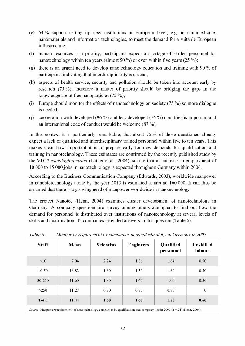
The project Nanotec (Henn, 2004) examines cluster development of nanotechnology in Germany. A company questionnaire survey among others attempted to find out how the demand for personnel is distributed over institutions of nanotechnology at several levels of skills and qualification. 42 companies provided answers to this question (Table 6).
Table 6: Manpower requirement by companies in nanotechnology in Germany in 2007
Staff Mean Scientists Engineers Qualified personnel
Unskilled labour
<10 7.04 2.24 1.86 1.64 0.50
10-50 18.82 1.60 1.50 1.60 0.50
50-250 11.60 1.80 1.60 1.00 0.50
>250 11.27 0.70 0.70 0.70 0
Total 11.44 1.60 1.60 1.50 0.60
Source: Manpower requirements of nanotechnology companies by qualification and company size in 2007 (n = 24) (Henn, 2004).
33
0
2
4
6
8
10
12
14
16
18
20
AT BE BG CZ DK FR DE EL HU IL IT NL NO PL SI SE CH TR UK
Number
Source : Nanoforum, 2005, p. 9.
Enterprises in nanotechnology, irrespective of their size, indicate roughly an equally strong demand for natural scientists, engineers and intermediate qualified workers for 2007. Staff are required on a short- and medium-term basis as much as graduates but, semi- and unskilled personnel are little needed, so employers first ask for well-qualified personnel with advanced and intermediate qualifications.
4.4. Skill needs in nanotechnology
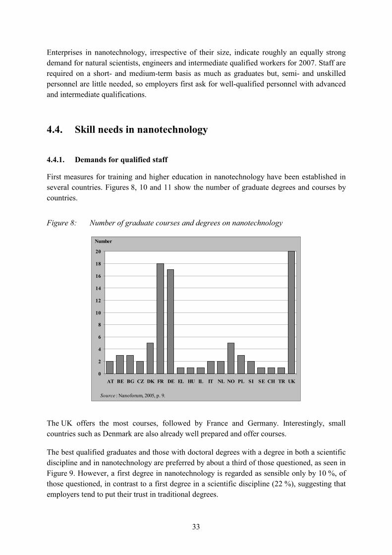
4.4.1. Demands for qualified staff
First measures for training and higher education in nanotechnology have been established in several countries. Figures 8, 10 and 11 show the number of graduate degrees and courses by countries.
Figure 8: Number of graduate courses and degrees on nanotechnology
The UK offers the most courses, followed by France and Germany. Interestingly, small countries such as Denmark are also already well prepared and offer courses.
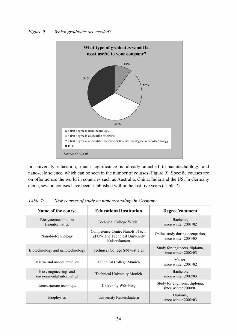
The best qualified graduates and those with doctoral degrees with a degree in both a scientific discipline and in nanotechnology are preferred by about a third of those questioned, as seen in Figure 9. However, a first degree in nanotechnology is regarded as sensible only by 10 %, of those questioned, in contrast to a first degree in a scientific discipline (22 %), suggesting that employers tend to put their trust in traditional degrees.
34
What type of graduates would be most useful to your company?
10%
22%
34%
34%
a first degree in nanotechnologya first degree in a scientific discipline
a first degree in a scientific discipline with a masters degree in nanotechnologyPh.D.
Source : ENA, 2005
Figure 9: Which graduates are needed?
In university education, much significance is already attached to nanotechnology and nanoscale science, which can be seen in the number of courses (Figure 9). Specific courses are on offer across the world in countries such as Australia, China, India and the US. In Germany alone, several courses have been established within the last five years (Table 7).
Table 7: New courses of study on nanotechnology in Germany
Name of the course Educational institution Degree/comment
Biosystemtechniques Bioinformatics Technical College Wildau Bachelor,
since winter 2001/02
Nanobiotechnology Competence Centre NanoBioTech, ZFUW and Technical University
Kaiserslautern
Online study during occupation, since winter 2004/05
Biotechnology and nanotechnology Technical College Südwestfalen Study for engineers, diploma, since winter 2002/03
Micro- and nanotechniques Technical College Munich Master, since winter 2001/02
Bio-, engineering- and environmental informatics Technical University Munich Bachelor,
since winter 2002/03
Nanostructure technique University Würzburg Study for engineers, diploma, since winter 2000/01
Biophysics University Kaiserslautern Diploma, since winter 2002/03
35
Undergraduate degrees and courses
0
2
4
6
8
10
CZ DK DE IL PL SE CH UK
Number
Source : Nanoforum, 2005, p. 10.
Name of the course Educational institution Degree/comment
Nanostructure science – nanostructure
and molecular science University Kassel Diploma,
since winter 2003/04
Micro- and nanostructures University of the Saarland Diploma, since winter 2000/01
Nanomolecular science International University Bremen Master, since 2003
Biophysics, nanosciences, molecular biotechnology University Bielefeld Experimental Bachelor,
since winter 2004/05
Engineer nanotechnology Bundesagentur für Arbeit Nürnberg Diploma (University)
Molecular science University Erlangen- Nürnberg Bachelor/Master
Hard body physics and nanotechnology University Munich Diploma
Source: isw figure
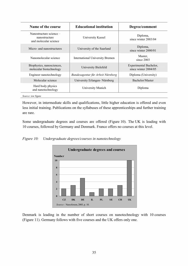
However, in intermediate skills and qualifications, little higher education is offered and even less initial training. Publications on the syllabuses of these apprenticeships and further training are rare.
Some undergraduate degrees and courses are offered (Figure 10). The UK is leading with 10 courses, followed by Germany and Denmark. France offers no courses at this level.
Figure 10: Undergraduate degrees/courses in nanotechnology
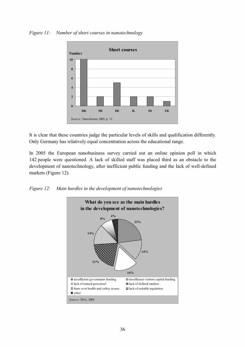
Denmark is leading in the number of short courses on nanotechnology with 10 courses (Figure 11). Germany follows with five courses and the UK offers only one.
36
Short courses
0
2
4
6
8
10
DK FR DE IL ES UK
Number
Source : Nanoforum, 2005, p. 11.
What do you see as the main hurdles in the development of nanotechnologies?
23%
14%
16%
21%
14%
8%4%
insufficient government funding insufficient venture capital fundinglack of trained personnel lack of defined marketsfears over health and safety issues lack of suitable regulationother
Source : ENA, 2005.
Figure 11: Number of short courses in nanotechnology
It is clear that these countries judge the particular levels of skills and qualification differently. Only Germany has relatively equal concentration across the educational range.
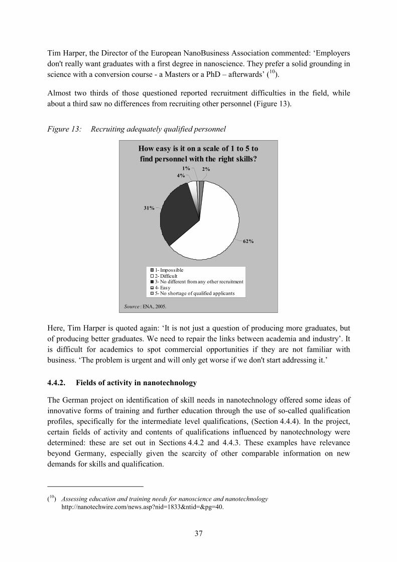
In 2005 the European nanobusiness survey carried out an online opinion poll in which 142 people were questioned. A lack of skilled staff was placed third as an obstacle to the development of nanotechnology, after inefficient public funding and the lack of well-defined markets (Figure 12).
Figure 12: Main hurdles in the development of nanotechnologies
37
How easy is it on a scale of 1 to 5 to find personnel with the right skills?
2%1%4%
62%
31%
1- Impossible2- Difficult3- No different from any other recruitment4- Easy5- No shortage of qualified applicants
Source : ENA, 2005.
Tim Harper, the Director of the European NanoBusiness Association commented: ‘Employers don't really want graduates with a first degree in nanoscience. They prefer a solid grounding in science with a conversion course - a Masters or a PhD – afterwards’ (10).
Almost two thirds of those questioned reported recruitment difficulties in the field, while about a third saw no differences from recruiting other personnel (Figure 13).
Figure 13: Recruiting adequately qualified personnel
Here, Tim Harper is quoted again: ‘It is not just a question of producing more graduates, but of producing better graduates. We need to repair the links between academia and industry’. It is difficult for academics to spot commercial opportunities if they are not familiar with business. ‘The problem is urgent and will only get worse if we don't start addressing it.’
4.4.2. Fields of activity in nanotechnology
The German project on identification of skill needs in nanotechnology offered some ideas of innovative forms of training and further education through the use of so-called qualification profiles, specifically for the intermediate level qualifications, (Section 4.4.4). In the project, certain fields of activity and contents of qualifications influenced by nanotechnology were determined: these are set out in Sections 4.4.2 and 4.4.3. These examples have relevance beyond Germany, especially given the scarcity of other comparable information on new demands for skills and qualification.
(10) Assessing education and training needs for nanoscience and nanotechnology
http://nanotechwire.com/news.asp?nid=1833&ntid=&pg=40.
38
New demands in nanotechnology are beginning to emerge in work areas that are important for nanotechnological companies and also educational institutions,. This involves R&D, production and manufacturing, quality assurance, documentation and marketing and distribution as described briefly below.
4.4.2.1. Research and development (R&D)
Currently, R&D is the most dominant field of work in nanotechnology and nanoscale science respectively. In general, that is because it is a relatively new field of research. It is also because new nanoanalytical methods such as the scanning tunnelling microscope (STM), make it even possible to manipulate single atoms, have been available for only a short time. For this invention Gerd Binning and Heinrich Rohrer were awarded the Nobel Prize in 1986. By this nanoanalysis, chemical processes, physical effects, biological principles and materials of all kind can be examined down to atom-scale range of size, leading to specific R&D activities.
4.4.2.2. Production and manufacture
Nanotechnological intermediary and final products are already produced in several branches, such as nanoparticles or nanosurface coatings. Further products are also expected. Here automation is increasing and process control is becoming increasingly complex and meaningful.
4.4.2.3. Quality assurance
Since nanotechnology is a new area, few quality standards exist so far. Nevertheless, working with nanoscale objects requires special working conditions, e.g. clean rooms, which demand meeting high quality standards. This includes dealing with special protective clothing and materials and substances.
4.4.2.4. Documentation
Dealing with special nanotechnological data also requires specific corresponding data processing, e.g. information management systems in the laboratory or the use of databanks with nanotechnological parameters. Both literature and online research into different nanotechnological aspects are carried out in documentation activities.
4.4.2.5. Marketing and distribution
Nanotechnological products and service are very explanation-intensive. A combination of nanotechnological, customer-related knowledge and commercial competences are increasingly in demand.
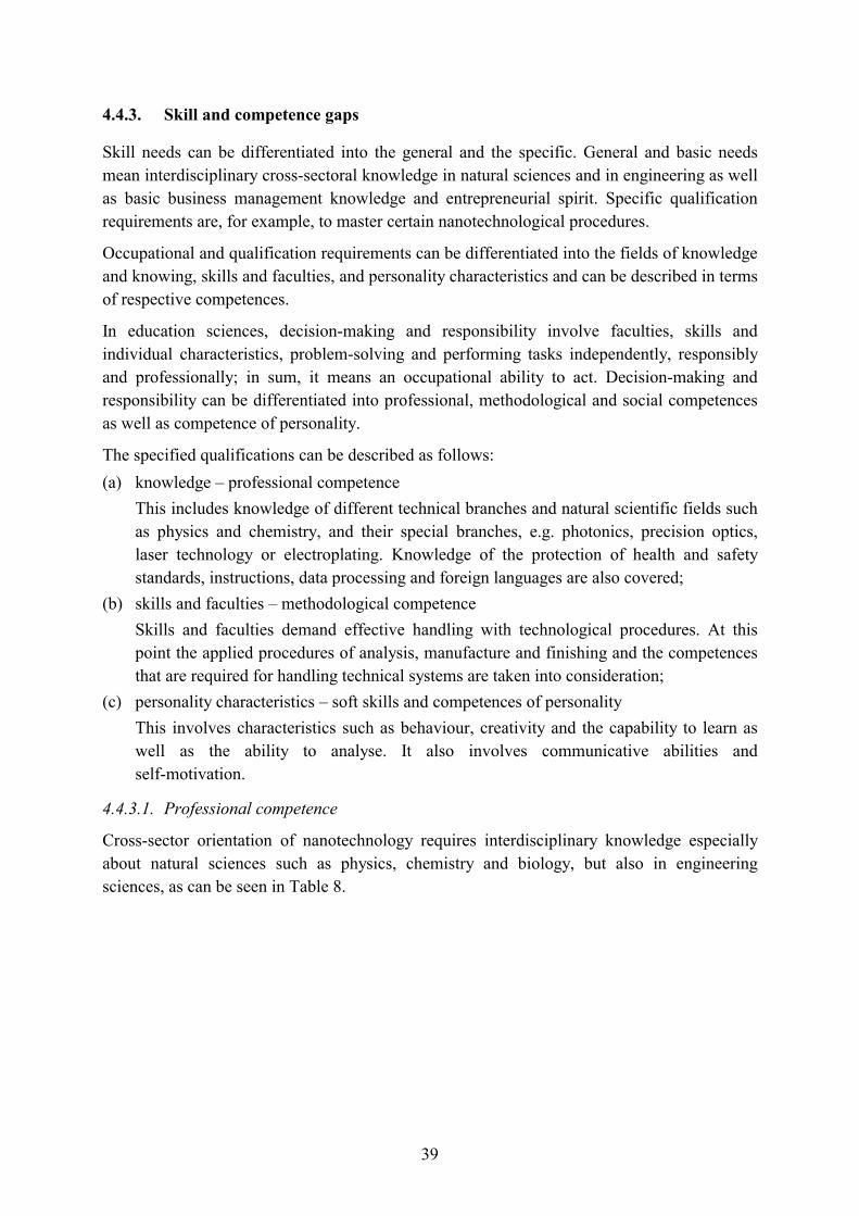
39
4.4.3. Skill and competence gaps
Skill needs can be differentiated into the general and the specific. General and basic needs mean interdisciplinary cross-sectoral knowledge in natural sciences and in engineering as well as basic business management knowledge and entrepreneurial spirit. Specific qualification requirements are, for example, to master certain nanotechnological procedures.
Occupational and qualification requirements can be differentiated into the fields of knowledge and knowing, skills and faculties, and personality characteristics and can be described in terms of respective competences.
In education sciences, decision-making and responsibility involve faculties, skills and individual characteristics, problem-solving and performing tasks independently, responsibly and professionally; in sum, it means an occupational ability to act. Decision-making and responsibility can be differentiated into professional, methodological and social competences as well as competence of personality.
The specified qualifications can be described as follows: (a) knowledge – professional competence
This includes knowledge of different technical branches and natural scientific fields such as physics and chemistry, and their special branches, e.g. photonics, precision optics, laser technology or electroplating. Knowledge of the protection of health and safety standards, instructions, data processing and foreign languages are also covered;
(b) skills and faculties – methodological competence Skills and faculties demand effective handling with technological procedures. At this point the applied procedures of analysis, manufacture and finishing and the competences that are required for handling technical systems are taken into consideration;
(c) personality characteristics – soft skills and competences of personality This involves characteristics such as behaviour, creativity and the capability to learn as well as the ability to analyse. It also involves communicative abilities and self-motivation.
4.4.3.1. Professional competence
Cross-sector orientation of nanotechnology requires interdisciplinary knowledge especially about natural sciences such as physics, chemistry and biology, but also in engineering sciences, as can be seen in Table 8.
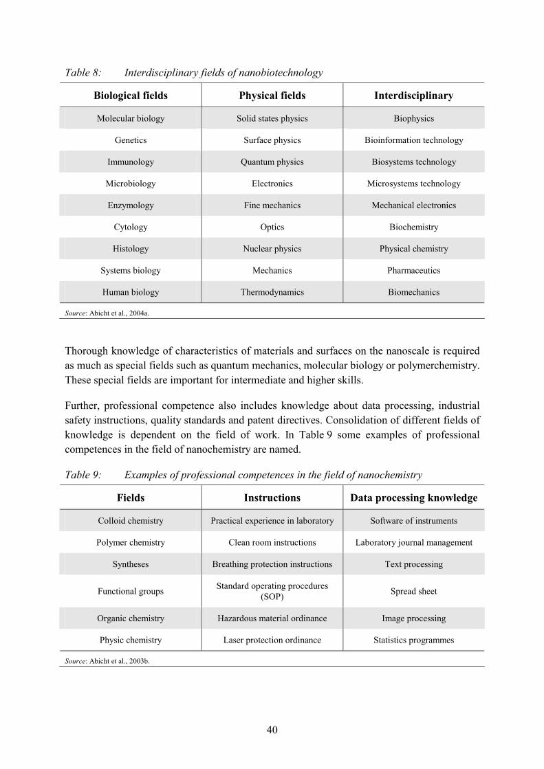
40
Table 8: Interdisciplinary fields of nanobiotechnology
Biological fields Physical fields Interdisciplinary
Molecular biology Solid states physics Biophysics
Genetics Surface physics Bioinformation technology
Immunology Quantum physics Biosystems technology
Microbiology Electronics Microsystems technology
Enzymology Fine mechanics Mechanical electronics
Cytology Optics Biochemistry
Histology Nuclear physics Physical chemistry
Systems biology Mechanics Pharmaceutics
Human biology Thermodynamics Biomechanics
Source: Abicht et al., 2004a.
Thorough knowledge of characteristics of materials and surfaces on the nanoscale is required as much as special fields such as quantum mechanics, molecular biology or polymerchemistry. These special fields are important for intermediate and higher skills.
Further, professional competence also includes knowledge about data processing, industrial safety instructions, quality standards and patent directives. Consolidation of different fields of knowledge is dependent on the field of work. In Table 9 some examples of professional competences in the field of nanochemistry are named.
Table 9: Examples of professional competences in the field of nanochemistry
Fields Instructions Data processing knowledge
Colloid chemistry Practical experience in laboratory Software of instruments
Polymer chemistry Clean room instructions Laboratory journal management
Syntheses Breathing protection instructions Text processing
Functional groups Standard operating procedures (SOP) Spread sheet
Organic chemistry Hazardous material ordinance Image processing
Physic chemistry Laser protection ordinance Statistics programmes
Source: Abicht et al., 2003b.
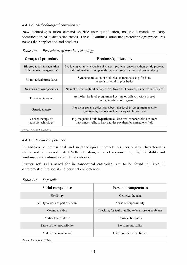
41
4.4.3.2. Methodological competences
New technologies often demand specific user qualification, making demands on early identification of qualification needs. Table 10 outlines some nanobiotechnology procedures names their application and products.
Table 10: Procedures of nanobiotechnology
Groups of procedure Products/applications
Bioproduction/fermentation (often in micro-organisms)
Producing complex organic substances, proteins, enzymes, therapeutic proteins - also of synthetic compounds, genetic programming and protein design
Biomimetical procedures Synthetic imitation of biological compounds, e.g. for bone or teeth material in prosthetics
Synthesis of nanoparticles Natural or semi-natural nanoparticles (micelle, liposome) as active substances
Tissue engineering At molecular level programmed culture of cells to restore tissues or to regenerate whole organs
Genetic therapy Repair of genetic defects at subcellular level by creeping in healthy genotype by vectors such as nanoparticles or virus
Cancer therapy by nanobiotechnology
E.g. magnetic liquid hyperthermia, here iron-nanoparticles are crept into cancer cells, to heat and destroy them by a magnetic field
Source: Abicht et al., 2004a.
4.4.3.3. Social competences
In addition to professional and methodological competences, personality characteristics should not be underestimated. Self-motivation, sense of responsibility, high flexibility and working conscientiously are often mentioned.
Further soft skills asked for in nanooptical enterprises are to be found in Table 11, differentiated into social and personal competences.
Table 11: Soft skills
Social competence Personal competences
Flexibility Complex thought
Ability to work as part of a team Sense of responsibility
Communication Checking for faults, ability to be aware of problems
Ability to empathise Conscientiousness
Share of the responsibility De-stressing ability
Ability to communicate Use of one’s own initiative
Source: Abicht et al., 2004b.
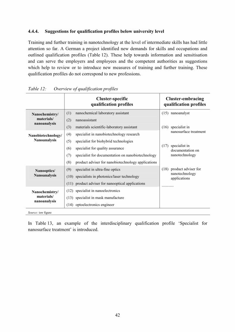
42
4.4.4. Suggestions for qualification profiles below university level
Training and further training in nanotechnology at the level of intermediate skills has had little attention so far. A German a project identified new demands for skills and occupations and outlined qualification profiles (Table 12). These help towards information and sensitisation and can serve the employers and employees and the competent authorities as suggestions which help to review or to introduce new measures of training and further training. These qualification profiles do not correspond to new professions.
Table 12: Overview of qualification profiles
Cluster-specific qualification profiles
Cluster-embracing qualification profiles
Nanochemistry/ materials/
nanoanalysis
(1) nanochemical laboratory assistant
(2) nanoassistant
(3) materials scientific-laboratory assistant
Nanobiotechnology/ Nanoanalysis
(4) specialist in nanobiotechnology research
(5) specialist for biohybrid technologies
(6) specialist for quality assurance
(7) specialist for documentation on nanobiotechnology
(8) product adviser for nanobiotechnology applications
Nanooptics/ Nanoanalysis
(9) specialist in ultra-fine optics
(10) specialists in photonics/laser technology
(11) product adviser for nanooptical applications
Nanochemistry/ materials/
nanoanalysis
(12) specialist in nanoelectronics
(13) specialist in mask manufacture
(14) optoelectronics engineer
(15) nanoanalyst
(16) specialist in nanosurface treatment
(17) specialist in documentation on nanotechnology
(18) product adviser for nanotechnology applications
............
Source: isw figure
In Table 13, an example of the interdisciplinary qualification profile ‘Specialist for nanosurface treatment’ is introduced.
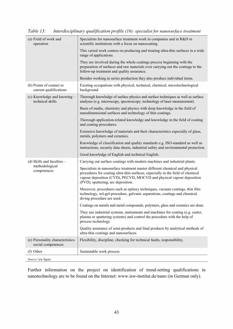
43
Table 13: Interdisciplinary qualification profile (16): specialist for nanosurface treatment
(a) Field of work and operation
Specialists for nanosurface treatment work in companies and in R&D in scientific institutions with a focus on nanocoating.
This varied work centres on producing and treating ultra-thin surfaces in a wide range of applications.
They are involved during the whole coatings process beginning with the preparation of surfaces and raw materials over carrying out the coatings to the follow-up treatment and quality assurance.
Besides working in series production they also produce individual items.
(b) Points of contact to current qualifications
Existing occupations with physical, technical, chemical, microtechnological background
(c) Knowledge and knowing – technical skills
Thorough knowledge of surface physics and surface techniques as well as surface analyses (e.g. microscopy, spectroscopy, technology of laser measurement).
Basis of maths, chemistry and physics with deep knowledge in the field of nanodimensional surfaces and technology of thin coatings.
Thorough application-related knowledge and knowledge in the field of coating and coating procedures.
Extensive knowledge of materials and their characteristics especially of glass, metals, polymers and ceramics.
Knowledge of classification and quality standards e.g. ISO-standard as well as instructions, security data sheets, industrial safety and environmental protection.
Good knowledge of English and technical English.
(d) Skills and faculties – methodological competences
Carrying out surface coatings with modern machines and industrial plants.
Specialists in nanosurface treatment master different chemical and physical procedures for coating ultra-thin surfaces, especially in the field of chemical vapour deposition (CVD), PECVD, MOCVD and physical vapour deposition (PVD), sputtering, arc deposition.
Moreover, procedures such as epitaxy techniques, vacuum coatings, thin film technology, sol-gel-procedure, galvanic separations, coatings and chemical diving procedure are used.
Coatings on metals and metal compounds, polymers, glass and ceramics are done.
They use industrial systems, instruments and machines for coating (e.g. caster, plasma or sputtering systems) and control the procedure with the help of process technology.
Quality assurance of semi-products and final products by analytical methods of ultra-thin coatings and nanosurfaces.
(e) Personality characteristics- social competences
Flexibility, discipline, checking for technical faults, responsibility.
(f) Other Sustainable work process
Source: isw figure
Further information on the project on identification of trend-setting qualifications in nanotechnology are to be found on the Internet: www.isw-institut.de/nano (in German only).
44
4.5. Implementing and verifying education and training across Europe
Improvement of training and further training in nanotechnology is presented in the following six steps. Some of these points have been already discussed in this study.
4.5.1. Analysis of nanotechnology and its institutions in Europe and worldwide
The first step demonstrates what nanotechnology means and where in Europe it is used, taking into account the present state of nanotechnology, prognoses and estimates of the economic viability of several main focuses. In this way European nanotech-companies and scientific institutions, cooperative associations and networks of nanotechnology can be detailed.
The European Commission has recognised the economic significance of nanotechnology and applies new standards for its development in Europe in its policy paper Towards a European strategy for nanotechnology. Nanotechnological applications take place in many different branches such as materials science, information technology, health service, diagnosis devices, energy, safety and space travel.
In the research support Sixth Framework Programme (FP6) the EU explicitly plans to push the development of nanotechnology (11).
The call for consultation process of the EU of 12 May 2004 points out development tendencies and focuses on all sectors affected by nanotechnology. It centres on investment in human resources in particular. Nanotechnology, as a new and dynamic field, presents a golden opportunity to attract a greater number of young scientists and other skilled personnel to careers in research (EC, 2004a, p. 14).
4.5.2. Survey of scientific-technological development
Once the institutions of nanotechnology are mapped, the scientific-technological developments and trends have to be analysed. Therefore, instruments for registration, assessment and classification of nanotechnological manifestations throughout Europe, namely technological procedures, products, natural scientific principles, etc., are needed. In the authors’ view the systematisation matrix can provide these instruments. A systematic survey on nanotechnology should be created, from which demands for qualification can be deduced.
(11) Examples of project support by the EU are the following nanotechnology projects:
Microchem deals with the controlling of water treatment by means of chemical analyses; DNA arrays and biochips are used in genome research, research into diseases and the development of
medicine; PolymerMicroSensorFab deals with the development of a one-way-biochips for low-cost DNA analysis; Nanomag deals with the development of corrosion-resistant coatings on the basis of magnesium alloy for
automobiles.
45
It can also serve the transfer of knowledge between science-science and economy-economy as well as science-economy and, therefore, the building of cooperative associations and networks.
4.5.3. Identification of new demands for qualifications (competences)
This step centres on the identification of current skill needs and new requirements for qualifications. The findings gained from the steps I and II are to be taken into account. Trend-setting developments of nanotechnology, relevant fields of application, and job and work systems in companies and institutions of nanotechnology give rise to new job requirements which constitute the basis for identification new skill needs. These are differentiated according to professional competence into knowledge, according to methodological competence - namely skills and faculties – and into social competence as well as competence of personality, to which soft skills belong.
4.5.4. Development of qualification profiles
Qualification profiles contain characteristics of knowledge, skills and faculties, which are a prerequisite for certain jobs in nanotechnology. They cover recommendations for further education, the development of intermediate qualifications and possibly also academic degrees.
The construction of qualification profiles should be modular. A corresponding acknowledgement of degrees at international level can be guaranteed by the use of a recognised credit-transfer system, e.g. the European credit transfer system (ECTS), for academic recognition, allowing transparency and recognition of vocational education and training can be promoted. Besides validation and recognition of training by a credit transfer system, a qualitative assessment and validation of prior learning should be conducted to stress more strongly the didactic approach/method of training measures.
4.5.5. Development and testing of new education and training measures throughout Europe
New demands for qualifications are the basis for developing innovative measures in education and training. After a testing phase, new forms and contents of education and further education could be implemented throughout Europe. At work level, a structure of qualification offers should be developed and implemented by modifying present qualifications or creating new measures of training and further training, e.g. by a modular system. Therefore, certain consequences for initial and continuing vocational training throughout Europe arise:
(a) initial vocational education and training (modification, reorganisation, new vocational training, new bachelor courses);
(b) further training (new modules, qualifications, modular qualification system).

46
Another – more rapid - approach would to develop modular courses of further training in different nanobranches, taking into account all relevant fields of work from R&D to quality assurance. These modules could be incorporated into several fields, such as nanochemistry/materials, nanobiotechnology, nanoelectronics and nanooptics. In addition, the modules of further training themselves should be combined and be based on each other.
An example of contents of these modules can be found in Table 14. The modules can be combined, as shown, either in horizontal or in vertical reading depending on the need.
Table 14: Model of further education modules in nanotechnology Introduction/
basics Research and development
Production/ process
Quality assurance Documentation
Nanochemistry/ Materials
Nano Modul
Nano Modul
Nano Modul
Nano Modul
Nano Modul
Nanobio- technology
Nano Modul
Nano Modul
Nano Modul
Nano Modul
Nano Modul
Nanoelectronics Nano Modul
Nano Modul
Nano Modul
Nano Modul
Nano Modul
Nanooptics Nano Modul
Nano Modul
Nano Modul
Nano Modul
Nano Modul
Source: isw figure
4.5.6. Generalisation and broad implementation of new education and training measures
To verify and apply new education and training measures, implementation models – specifically developed and tested – are needed. Further, European standards that provide content and quality of qualifications are also needed.
47
5. Conclusions
1. Nanotechnology is not a mere reduction of existing technologies. It is based on different working principles and theoretical models from traditional technologies, including microtechnologies. A particular characteristic is the application of quantum effects as well as self-organisation processes. Nanotechnological skill and qualification needs reflect this change of paradigms and transfer them into applications relevant for production. Potential ethical, medical and ecological aspects of this new technology also have to be taken into account.
2. Measures to increase public perception and acceptance of the new technology are needed to transport the distribution of the nanotechnology as the key technology of the 21st century and create conditions to provide qualified staff. Therefore, pupils and students should already be targeted for the new technology. Further, employees should be trained in nanotechnology.
3. Specific knowledge and qualifications are needed particularly for the production of nanotechnological products and the control of nanotechnological production methods. However, it is not recognised that users of nanotechnological products need special qualifications at present. At this point nanotechnology is basically different from the information technologies that caused broad qualification demands for users.
4. Nanotechnology as production technology is currently in a transitional phase from basic research or applied science to production. At this stage of development only first attempts can be defined regarding the medium-term demand for personnel with intermediate-level qualifications.
5. The current scope of research activities in nanotechnology is the reason for the high demand for personnel with primarily university degrees. The demand for staff with qualifications below university level is comparatively low at present. Nevertheless, the study records a number of cases of lack of qualified staff below university level.
6. With the extension of nanotechnological production there is a good chance for structural changes in enterprises. Because of a high degree of automation, such work activities as process control, quality assurance and documentation will increasingly be assigned to qualified employees with a qualification below university level. New fields of activity occur in the area of marketing and sales. Financial points of view (wage costs) are important for the assignment of work tasks to employees with qualifications below university level. Employees with lower qualifications incur lower wage costs.
7. Employees with qualifications below university level need particular interdisciplinary knowledge and strong social competences to take part in cooperation and innovation processes in the enterprises.
48
8. At the moment the required knowledge and skill components are mainly offered in the form of additional qualifications, building on the basis of existing qualifications (occupations) in the fields of physics, chemistry or biology. Because of the comparatively low number of those involved, this form of training will further dominate in the short-term. In the short term, modular training offers or a further training system are needed.
9. With the increasing demand for employees with qualifications below university level (number of people) as well as with the increasing need for integration of new knowledge components, it can be expected that enrichment of existing qualification by additional knowledge and skills (courses) does not qualitatively satisfy enterprises any more. It is time for the innovation of occupational profiles and the subsequent construction of new qualifications. Typical features of nanotechnology, such as work with quantum effects or processes of self-organisation, are at the heart of those occupations.
10. Nanotechnology is currently a largely heterogeneous field of research and work with different influences arising from nanoelectronics, nanochemistry, nano-biotechnology, nanooptics and nanoanalyses. A systemic basis is needed to summarise the variety of nanotechnological appearances to develop qualification profiles, new occupations and modular training offers. Such a systemic approach can be developed by using theoretical models of the general technology.
11. International comparison reveals extensive public promotion of natural sciences and technology research, but few activities to identify and develop necessary human resources. As far as these activities are promoted, they are usually a component of scientific or technological research and lead to individual solutions without involving neighbouring areas in a systematic manner. This can cause a shortage of qualified personnel in the medium term. A shortage of qualified staff could be a limiting factor for the successful transition from nanotechnological research to nanotechnological production.
12. A significant proportion of public funds (e.g. 5 %) should be used to identify skill needs and to develop and test training to prevent obstacles to the economic utilisation of research results through a shortage of human resources. Individual solutions are to be augmented by a systemic approach both for initial education and for further training. A monitoring programme is urgently recommended to identify skill needs from qualitative and quantitative points of view. The results should be transferred into an action plan for education and training. Additionally the ESF could be used to develop and test practical training measures.
13. Institutions for vocational education and training, centres of excellence and exchange of best practice in the area of nanotechnology should be more strongly promoted in Europe.
49
List of abbreviations
AFM Atomic force microscope AMD Advanced micro devices ANF Asia nano forum BMBF Bundesministerium für Bildung und
Forschung BMVIT Federal Ministry for Transport, Innovation
and Technology CC Competence centres CCN Competence centres on nanotechnology CNT Fraunhofer Centre for Nanoelectronic
Technologies CVD Chemical vapour deposition DCTC Dakota County technical college DGB German confederation of trade unions DNA Deoxyribonucleic acid EBL Electron beam lithography EC European Commission ECTS European credit transfer system ENA European NanoBusiness Association ENIAC European nanoelectronic initiative
advisory Council ESF European Social Fund EU European Union EUL Extreme ultraviolet light EUR-OP Office for official publications of the
European Communities EUVL Extreme ultraviolet lithography FRAM Ferroelectric random access memory GNN Global Nanotechnology Network IBM International Business Machines ICs Integrated circuits LED Light emitting diode LETI Laboratory of electronics and information
technologies MEMS Microelectro mechanical systems MNT National micro- and nanotechnology MOCVD Metal organic chemical vapour deposition
MRAM Magneto resistive random access memory MRI Materials research internships for minority
undergraduates MWM Materials world modules programme MWNT Multiwalled nanotube NCLT National centre for learning and teaching NEMS Nanoelectromechanical systems NNI National nanotechnology initiative NSEE Nanoscale science and engineering
education NSET Nanoscale science, engineering and
technology NSF National science foundation OLED Organic light emitting diode PECVD Plasma enhanced chemical vapour
deposition PLED Polymer light emitting diode PRAM Permanent random access memory PVD Physical vapour deposition QD Quantum-dot REST Research experience for science teachers REU Research experience for undergraduates RFID Radio frequency identification SAM Self-assembled monolayers SOP Standard operating procedures SPM Scanning probe technique SPN Scanning probe nanolithography STM Scanning tunnelling
microscope/microscopy STX Saxitoxin SWNT Single walled nanotube TSMC Taiwan semiconductor manufacturing
Company UFS Ultra-thin functional coatings UPOB Ultra-precise surface treatment WTEC World technology
50
References Abicht, L. et al. Ermittlung von Trendqualifikationen als Basis zur Früherkennung von Qualifikationsentwicklungen Ziele – theoretische Frundlagen – Vorgehensweise. Halle: isw, 1998.
Abicht, L.; Schlicht, E.; Schumann, U. Entwicklung einer Systematisierungsmatrix für die Nanotechnologie zur Identifikation von Trendqualifikationen. Halle: isw, 2003a.
Abicht, L.; Schlicht, E.; Schumann, U. Untersuchungscluster: Nanochemie/Materialien und Nanoanalytik. Halle: isw, 2003b.
Abicht, L.; Schlicht, E.; Schumann, U. Untersuchungscluster: Nanobiotechnologie und Nanoanalytik. Halle: isw, 2004a.
Abicht, L.; Schlicht, E.; Schumann, U. Untersuchungscluster: NanoOptik und Nanoanalytik. Halle: isw, 2004b.
Abicht, L.; Schlicht, E.; Schumann, U. Abschlussbericht Trendqualifikationen im Bereich der Nanotechnologie. Halle: isw, 2005.
Bachmann, G. Innovationsschub aus dem Nanokosmos: Technologieanalyse. Düsseldorf: VDI-Technologiezentrum, Abt. Zukünftige Technologien, 1998.
Bachmann, G. Überblick: Forschungsbereiche und Anwendungsfelder. VentureCapital Magazin ‘Nanotechnologie’, 2002, p. 18-22.
BMBF–Bundesministerium für Bildung und Forschung. Nanotechnologie erobert Märkte. Deutsche Zukunftsoffensive für Nanotechnologie. Berlin: BMBF, 2004 Available from Internet: www.bmbf.de/pub/zukunftsoffensive_nanotechnologie.pdf [cited 7.10.2005].
Drexler, K.E. Das molekulare Fließband. Spektrum der Wissenschaft Spezial 2/01, 2001, p. 64-65.
EC – European Commission. Towards a European strategy for nanotechnology. Luxembourg: EUR-OP, 2004a. Available from Internet: http://europa.eu.int/comm/research /industrial_technologies/pdf/nanotechnology_communication_en.pdf [cited 7.10.2005].
EC – European Commission. Vision 2020 Nanoelectronics at the centre of change. Luxembourg: EUR-OP, 2004b. Available from Internet: http://europa.eu.int/comm/research/ industrial_technologies/pdf/nanoelectronics_june2004_en.pdf [cited 7.10.2005].
EC – European Commission. Nanosciences and nanotechnologies: an action plan for Europe 2005-2009. Brussels: European Commission, 2005 (COM(2005) 243).
Edwards, S. Biomedical applications of nanoscale devices. Report. Norwalk, Connecticut: Business Communication Company, 2003.
ENA – European NanoBusiness Association. The 2005 European NanoBusiness. Brussels: ENA, 2005. Available from Internet: www.nanoeurope.org/files/The%202005%20European %20NanoBusiness%20Survey.pdf [cited 7.10.2005].
51
Folea, A. Survey of networks in nanotechnology. Brussels: European Commission, Research DG, 2003.
Grupp, H. Technologie am Beginn des 21. Jahrhunderts. Heidelberg: Physica-Verl., 1995.
Hartmann, U. Nanobiotechnologie: eine Basistechnologie des 21. Jahrhunderts. Saarbrücken: Zentrale für Produktivität und Technologie Saar, 2001.
Heimer, T.; Malanowski, N. Nanotechnologie als wirtschaftlicher Wachstumsmarkt. VentureCapital Magazin ‘Nano-/Mikrotechnologie’, October 2003, p. 32-33.
Henn, S. Gründungen in der Nanotechnologie. Clusterentwicklung und Förderung. isw-workshop ‘Nanobiotechnologie Entwicklungstendenzen und Qualifikationsanforde-rungen’, Berlin, 15.4.2004.
Hinze, S.; Gaisser, S. Nanotechnologie und Life Sciences. Study in the context of TAB project ‘Nanotechnologie’. Karlsruhe: Fraunhofer ISI, 2003.
Horx, M. Aufbruch in die Nano-Welt Nanotechnologie macht schnellere Fortschritte als erwartet. Der Zukunftsletter, 2001, No 9, p. 6-7.
Ilfrich, T.; Kunert, G. Nano + Mikrotech II. Entwicklung der Nano- und Mikrotechnologie. Berlin: BoD GmbH, Norderstedt, 2005.
Jopp, K. Nanotechnologie – Aufbruch ins Reich der Zwerge. Wiesbaden: Gabler, 2003.
Lauterwasser, Ch. (ed.) Small sizes that matter: opportunities and risks of nanotechnologies. Report in cooperation with the OECD international future programme. Munich/Paris: Allianz AG/OECD, 2005.
Luther, W. Marktpotentiale in der Nanotechnologie. VentureCapital Magazin ‘Nano-/Mikro-technologie’, 2003, p. 27-29.
Luther, W. et al. Nanotechnologie als wirtschaftlicher Wachstumsmarkt. Innovations- und Technikanalyse. Düsseldorf: Zukünftige Technologien Consulting der VDI Technologie-zentrum, 2004.
Malanowski, N.; Zweck, A. Nanotechnologie aus der Perspektive der Innovations- und Technikanalyse. TA-Datenbank-Nachrichten, 2001, No 3/10, p. 82-85.
Malsch, J.; Oud, M. Outcome of the open consultation of the European strategy for nanotechnology. Düsseldorf: Nanoforum, 2004.
Mazolla, L. Commercializing nanotechnology. Nature Biotechnology, 2003, No 10/03, p. 1137-1143.
Meridian Institute. International dialogue on responsible research and development of nanotechnology. Final report. Washington DC: Meridian Institute, 2004.
Müller, G.; Righi, M.L. Nanochemie und Nanomaterialien. VentureCapital Magazin ‘Nanotechnologie’, 2002, p. 28-29.
Nanoforum. European nanotechnology education catalogue. Düsseldorf: Nanoforum, 2005.
52
Presidents Council of Advisors on science and technology. The national nanotechnology initiative at five years. Washington DC: Office of Science and Technology Policy, 2005. Available from Internet: www.ostp.gov/PCAST/PCASTreportFINALlores.pdf [cited 7.10.2005].
Schlicht, E.; Schumann, U. Ermittlung von Trendqualifikationen im Bereich der Nanotechnologie. In: Windelband, L.; Dworschak, B.; Schmidt, L. (eds) Qualifikationen für die Arbeit von morgen erkennen. Bielefeld: W. Bertelsmann Verlag, 2004.
Wolffgramm, H. Allgemeine Technologie. Vol. 1. Hilesheim: Verlag Franzbecker, 1994.
WTEC. Russian research and development activities on nanoparticles and nanostructured materials. Proceedings of WTEC workshop held in St. Petersburg, Russia, on 21 August 1997. Baltimore, Maryland: International Technology Research Institute, World Technology (WTEC) Division, 1997. Available from Internet: www.wtec.org/loyola/nano/Russia/ nanorussia.pdf [cited 7.10.2005].
Recommended links
www.nanotech-now.com Internationally focused platform offers general, economic and scientific information towards nanotechnology.
www.nanoforum.org European Internet portal with much information to different aspects of nanotechnology.
www.techportal.de German Internet portal to different fields of technology, especially the new competence centres on nanotechnology are introduced.
www.isw-institut.de/nano Homepage of the project Ermittlung von Trendqualifikationen im Bereich der Nanotechnologie (Identification of trend-setting qualifications in nanotechnology) throughout Germany.
53
Glossary Atom The smallest unit of a chemical element, about a third of a nanometer in diameter. Atoms
make up molecules and solid objects.
Atomic force microscopy (AFM)
Atomic force microscopy (AFM) is a technique for analysing the surface topography with a resolution down to the level of the atom. The AFM detects forces acting on a probe which is in mechanical contact with the surface using a small spring or cantilever. The probe is scanned line by line over the area of interest, whereby the topography is derived from the bending or deflection of the cantilever. The AFM is closely related to another scanning probe technique (SPM), called scanning tunnelling microscopy (STM). The difference is that AFM does not require a conductive sample, whereas STM does. AFM is being used to understand materials problems in many areas, including data storage, telecommunications, biomedicine, chemistry, and aerospace.
Bottom-up Using small building blocks (e.g. atoms or molecules) to create larger items or structures. Diametrical method of a top-down process, mainly used by nature in biological systems or by chemists to construct larger objects by combining molecules.
Catalyst A substance that increases the rate of a chemical reaction by reducing the activation energy, but which is left unchanged by the reaction. A catalyst works by providing a convenient surface for the reaction to occur. The reacting particles gather on the catalyst surface and 1) collide more frequently with each other; 2) more of the collisions result in a reaction between particles because the catalyst can lower the activation energy for the reaction.
Chemical vapour deposition (CVD)
A coating technique where coating material condenses from different gas phases and a chemical reaction is involved. Volatile chemicals are brought in a reaction chamber where the chemical reaction is initiated due to temperature, pressure or a plasma.
Chromatography Chromatography is a physical method of separation in which the components to be separated are distributed between two phases, one of which is stationary while the other moves in a definite direction. Chromatography is widely used for the separation, identification, and determination of the chemical components in complex mixtures.
Belgium BE Italy IT Austria AT Czech Republic CZ Cyprus CY Sweden SE
Denmark DK Latvia LV Poland PL Germany DE Lithuania LT Portugal PT
Estonia EE Luxembourg LU Slovenia SI Greece EL Hungary HU Slovakia SK
Spain ES Malta MT Finland FI France FR Netherlands NL United Kingdom UK
Country codes (ISO codes)
Ireland IE
Dendrimer A dendrimer (from Greek dendra for tree) is an artificially manufactured or synthesised branched molecule built up from monomers. Basically, a dendrimer is a polymer and its name is derived from ‘dendritic polymer’.
DNA Acronym for deoxyribonucleic acid, usually 2'-deoxy-5'-ribonucleic acid. The double-stranded DNA molecule carries the genetic information, which is encoded in a sequence of base pairs (adenine and thymine, guanine and cytosin).
Electron-beam lithography (EBL)
Similar to photolithography, but instead of light the focused electron beam of a scanning electron microscope is used to modify a sensitive layer (resist) which was cast on a silicon wafer e.g. A mask is not involved since the impact or dose of the electron beam can be adjusted, e.g. areas to be structured receive a higher dose.
54
Enzymes Molecular machines found in nature, made of proteins, which can catalyse (speed up) chemical reactions.
Epitaxy Production of geometrically perfect layers on a crystalline surface by evaporation or sputtering techniques. The evaporated layer forms a single crystal.
EUV/EUVL Extreme ultraviolet light. Extreme ultraviolet lithography (EUVL) allows the production of smaller transistors to the semiconductor industry.
Fullerene General name for a class of molecules based on pure carbon. Because some fullerenes take a shape similar to a soccer ball or a geodesic dome, it is sometimes referred to as a buckyball after the inventor of the geodesic dome, Buckminster Fuller (1895-1983), after whom the fullerene is more formally named. Sometimes referred to as Buckminsterfullerenes.
Interface In physics or chemistry: the area or boundary separating two phases, e.g. liquid-gas, solid-liquid, solid-gas or liquid-liquid.
LED, light emitting diode
A sandwich structure of two semi-conductors (p-n-junction). Light of a specific wavelength or colour is emitted from this junction when a current runs through it. The colour can be adjusted by choosing different semi-conductors and process engineering.
Lithography A general top-down method to write structures on a surface with a certain probe. This probe can be light in the case of the common photolithography or electrons when using electron-beam lithography. Literally, it means stone writing (Greek).
MEMS Acronym for microelectro mechanical systems. Refers to a technology used to integrate various electro-mechanical functions onto integrated circuits. A typical MEMS device combines a sensor and control logic to perform a monitoring function. Examples include sensing devices used to control the deployment of airbags in cars and switching devices used in optical telecommunications cables.
Molecular sieve Porous structures with adjustable pore size in the nanometer range, used to adsorb molecules from a liquid or a gas (see Zeolite) exhibiting the basic function of a nanoscaled filter.
Molecule The smallest unit of a certain material consisting of at least two or more atoms connected by chemical bonds. Their size ranges from several nanometers up to macroscopic dimensions. The typical unit manipulated by nanotechnology.
Nano A prefix meaning one billionth (1/1 000 000 000).
Nanoanalysis Nanoanalysis refers to special techniques for determining the atomic structures of materials. It is a cross sectional science supplies analytic methods and means for recording basic phenomena and for characterising products and, further, causes an analytical quality assurance by making a contribution to national and international standardisation. Nanoanalytical techniques offer many possibilities of making scientific information available to the fields of physics, chemistry, biology, materials science and engineering on nanometer scale. Steady miniaturisation absolutely requires understanding in and control of processes on the nanoscale.
55
Nanobiotechnology/nanomedical technology
Nanotechnology combines technological processes with the knowledge of biosystems at nano level. Two principal strategies can be used: the bio nano strategy, which uses scientific findings of biological systems as pattern for developing technological systems, in the sense of nanobionic; the nano bio strategy, that makes nanotechnological processes affect experience with biosystems persistently. Nanobiotechnology is a cross sectional technology. Important natural scientific fields linked with nanobiotechnology are, e.g., molecular biology, genetics, colloid chemistry, biochemistry, surface physics and quantum mechanics.
Nanochemistry /nanomaterials
Nanochemistry deals with creating and manipulating nanoactive chemical systems. Supramolecular functional systems are the basic principles for forming new materials. Nanochemistry – which is internationally not standardised – means chemical changes in systems, which work exclusively on the nanoscale. Nanochemistry specifically includes functional supramolecular systems e.g. transport of active agents, systems that can be switched or controlled, systems with characteristics which can be regulated, functional coatings, and the formation processes of nanoparticles (particles, colloids, fluids, nanotube).
Nanoelectronics Nanoelectronics is not subject to a strict definition because the transition from microelectronics to nanoelectronics is fluid. At this time microelectronics deals in the realm up to 90 nm. Integrate circuits (significant) below the 100 nm scale are called nanoelectronics. It is reckoned on a further miniaturisation (top-down approach) down to 23 nm (10-9 m) within the next decade. The optical lithography reaches its limits for physical laws (wavelength), so that a change in technology can be expected in the near future.
Nanoelectro-mechanical systems (NEMS)
An integrated electro-mechanical nanoscaled device similar to MEMS but with nanometer dimensions.
Nanolithography Nanolithography is the art and science of etching, writing, or printing at the nanoscopic level, where the dimensions of characters are on the order of nanometers. This includes various methods of modifying semiconductor chips at the atomic level for the purpose of fabricating integrated circuits (ICs). Instruments used in nanolithography include the scanning tunnelling microscope (STM) and the atomic force microscope (AFM). Both allow surface viewing in fine detail without necessarily modifying it. Either the STM or the AFM can be used to etch, write, or print on a surface in single-atom dimensions.
Nanometer (nm) One billionth of a meter (1/1,000,000,000).
Nanooptics Nanooptics includes the research, development and production of optical components, structures and systems on the nanometer scale. Nanooptics covers several branches such as ultraprecision optics that manufactures nanometer precise lenses and lens systems used in appliance optics and medical optics. Laser technology, which is used for optoelectronical components in the information and communication technology, is a further important branch.
In optics or photonics nanotechnological aspects are important at different places. Phontonics deals with technologies for production and application of light and other radiant energies, which are based upon photons. The range of application of photonics is many and diverse; it extends over energy production, detectors, telecommunications and informatics.
Nanoscale Concerning the molecular and macromolecular level. Generally, the nanoscale is defined from 1 to 100 nm, whereas the range from 100 to 1000 nm is named the submicrometer scale.
Nanotechnology Areas of technology where dimensions and tolerances in the range of 0.1 nm to 100 nm play a critical role.
56
Nanotubes Cylindrical tubelike molecule consisting of graphite sheets. They are extremely strong materials and have a good thermal conductivity. Carbon nanotubes are extremely thin (their diameter is about 10 000 times smaller than a human hair). A single walled nanotube (SWNT) is composed of one graphite sheet, a concentrical formation of more than one sheet is named multiwalled nanotube (MWNT).
OLED, organic light emitting diode
A light emitting device similar to a LED, but where the semiconductors were replaced by one or a stacked layer of organic thin films. The organic molecules emit light when a current is applied. Unlike LEDs, the OLED technology provides the possibility for the production of high resolution displays. Displays based on OLEDs are supposed to be faster, lighter, brighter and cheaper than the common LCD displays.
Photolithography The most common structuring method. Depositing a light sensitive layer on, e.g., a silicon wafer. Illuminating this layer through a mask and developing the structure in a final step. The result can be either the structures of the used mask or its opposite for a positive or negative resist, respectively.
Photonic crystal A material with periodic gaps or variations in the dielectric constant in the range of the wavelength of light. The propagation of light of a certain wavelengths is forbidden resulting in a photonic band gap, resembling the electrical properties of a semiconductor. Photonic crystals can be used as sensors, as light ducts or as optical switches in data communication.
Physical vapour deposition (PVD)
Coating method to deposit material on a surface. The most common methods are evaporation and sputtering. Evaporation is achieved in a vacuum chamber in which the evaporation is done thermally by heating the material above its melting point. Sputtering is done with a gas plasma. Ions from the plasma are accelerated towards the target surface releasing atoms from the target which condense on the sample surface (and everywhere else). The advantage of sputtering is a lower temperature compared to thermal evaporation.
Plasma The fourth state of aggregation of matter (thermal plasma). Beyond the gas state where at least a significant amount of atoms are ionised. A plasma consists of atoms, ions and electrons, but the overall charge is zero (quasi-neutral). This is the most common state of matter in the universe.
Proteins The chemical building blocks from which our cells, organs and tissues like muscle are made of. Proteins also serve double-duty as hormones, enzymes and antibodies, which help our bodies fight off invading germs. Proteins are made of long chains of even smaller building blocks called amino acids. Amino acids determine the size, shape, and length of protein molecules. They also give protein molecules the odd ability to coil and uncoil like tiny, cellular snakes.
RFID Radio frequency identification. A method of identifying unique items using radio waves. Typically, a reader communicates with a tag, which holds digital information in a microchip. But there are chipless forms of RFID tags that use material to reflect back a portion of the radio waves beamed at them.
Quantum dot A dot with an extension of several nanometer constructed of metallic or semiconductive material describing a nearly zero-dimensional object. These quantum dots have unique electrical properties, which can be used to store electrons or to transform the colour of light. The quantum dot is considered to have greater flexibility than other fluorescent materials, which makes it suited to use in building nanoscale computing applications where light is used to process information. They are made from a variety of different compounds, such as cadmium selenide.
57
Quantum well A theoretical concept to understand the quantum mechanical energy distribution and behaviour of nanoscaled bonded systems (e.g. energy levels of bonded electrons, tunnelling effect).
Quantum wire A nanoscaled conductive wire resembling a nearly 1-dimensional object with different electrical properties from those of macroscopic wires.
Scanning probe microscopy (SPM)
Generic name for different scanning microscopes, where a local probe collects surface or topography related information through a specific interaction between this probe and the surface under investigation. This interaction can be the tunnel current for STM or the force or damping of an oscillation in the case of an AFM, etc.
Scanning probe nanolithography (SPN)
Generic name for lithographic techniques based on scanning probe microscopes. This can be a scanning tunnelling microscope (STM) and the associated lithography is based on a pulsed bias voltage or an atomic force microscope (AFM) combined with a force or voltage based surface modifying technique.
Scanning tunneling microscope (STM)
A scanning probe technique where a local metallic probe is scanning a conductive surface. The topographic information is deduced from the tunnel current which runs between probe and sample without mechanical contact. The electron shells, or clouds, surrounding the atoms on the surface produce irregularities that are detected by the probe and mapped by a computer into an image.
Self-assembly Spontaneous aggregation of molecules or other particles to complex and ordered systems. Referred to as self-assembled monolayers (SAM) in the case of quasi two-dimensional aggregating systems. Although self-assembly and self-organisation are very similar, the term self-assembly is normally used for systems where covalent bonds are involved whereas self-organisation points to weakly interacting systems as they can be found, for example, in biological systems.
Self-organisation General term for weakly interacting systems where order is spontaneously increased (so called dissipative structures). An example is biological systems where complex and ordered structures are formed from comparatively simple building blocks (e.g. lipids in cell membranes). See also self-assembly.
Semiconductor A semiconductor is a substance, usually a solid chemical element or compound, which has conductivity between a metal and an isolator (e.g. silicon, germanium). Its conductivity is adjustable (doping) making it a good medium for the control of the electrical current.
Tissue engineering Tissue engineering is the application of the principles and methods of engineering and the life sciences toward the fundamental understanding of structure/function relationships in normal and pathological mammalian tissues and the development of biological substitutes to restore, maintain, or improve functions.
Top-down A general approach going from large items to smaller ones. The opposite of bottom-up. In a lithographic sense it means to produce micro- or nanoscaled structures using macroscopic instruments. The most common method is photolithography, which is capable of producing sub-100 nm features. Other examples are electron beam lithography (EBL) and scanning probe nanolithography (SPN).
Zeolite Any one of a family of hydrous aluminium silicate minerals, whose molecules enclose cations of sodium, potassium, calcium, strontium, or barium, or a corresponding synthetic compound, used chiefly as molecular filters and ion-exchange agents. See ‘molecular sieve’.
58
Annex 1: Selective research in nanotechnology
Nanoanalysis
Analysis using instruments gains increasingly significance compared to wet-chemical methods of study/analysis;
the degree of automation of analysis instruments is increasing despite increasing complexity;
there is an upward trend to full-scale analysis instruments and more effective mass analyses as, for example, in the research of active agents to high throughput screening – and to highly specialised analysis instruments with a rather small range of application;
the combination of different methods of proof in an analysis system gains increasingly importance, because they can measure several qualitative and/or quantitative parameters of a sample parallel and almost at the same time;
probe screening or microscopy; two trends begin to emerge. On the one hand the parallel use of several probes at the same time, and on the other the search for physics effects with which the picture quality of the probe screening microscopes can be improved.
Different methods of measurement and corresponding examples will be expounded by the following overview:
on an optical basis: microscopy, spectroscopy, photometry;
on an optoelectronical basis: electron microscope, AFM, saxitoxin (STX);
on a mechanical basis: analytic ultracentrifugation;
on the basis of (bio)chemical-physical interrelation: chromatography, electrophorese, volumetrics, viscosity;
on the basis of biological interrelation: detection or sequencing of DNA and amino acids (proteins) on the basis of characteristic bonds;
on the basis biohybridised principles: microarrays/biochips (protein chip, DNA chip, cellular chips, lab-on-a chip) and biosensors.
Life sciences, nanomedical technology/nanobiotechnology/cosmetic procedures
innovative methods of analysis and diagnosis, lab-on-a-chip technologies, biochips, protein chips allows among other things faster and low-price test methods with a small numbers of samples;
tissue engineering, prosthesis;
personalised drugs, e.g. specific medicine for the individual’s need;
59
innovative drugs and therapies, drug-delivery, drug-targeting, drug-release;
suntan lotions with high protection factor using nanoparticles of titanium and zinc oxide as additives;
skin cream with special lipoic acid, toothpaste, lipsticks;
anti-microbial coatings and sprays;
R&D based on the bottom-up principle taking biological systems as a model, for creating new and more effective production processes;
general change of paradigm in life sciences from genomics to proteomics;
development of functional biological nanocoatings, e.g. based on lotus effect or new biopolymers, which, e.g. give implants an immunologically compatible surface;
development of antibacterial nanocoatings for surgical instruments or lecterns;
improved catalysts, e.g. provided with molecular biological substances like certain enzymes by nanozeolite;
further research on microfluidity for controlled handling of even smaller quantities of fluids in the form of nanofluidity;
individual medicine that, according to therapies and treatment with drugs, takes the genetic background of each patient into account and, therefore, can improve the curative effect and reduce side effects at the same time or even be excluded at all. Critics are afraid of a lack of data protection, namely patients who have no secrets or even discrimination of genetically marginal groups;
tissue engineering for therapies of damaged tissue; biomemetic and bio-compatible materials allow therapies that fit exactly for teeth-, bone- and cartilage tissue in the sense of a regenerative medicine;
biomembranes with nanoscale pores, that are used as filter systems, e.g. in pharmaceutical parting of substances or at water treatment in ecology;
development of functional nanoparticles (liposomes, dendrimers) that are used as carriers for drugs or other substances and that can clearly improve not only their addressing, transport and measuring out but also their effectiveness; further ranges of application are effective contrast mediums in diagnostics and fillings in teeth and bones;
development of biosensors based on biomolecular interactions, that are designed as highly sensitive, precise and low-price; at an innovative form of biosensors cantilevers are immobilised on a sensor; contacting the objective molecule the sensor ‘bends’ and the resulting angle is measured by a laser. Can be applied, e.g., for analysis of respiratory tracts;
miniaturising and parallelising as well as the development of biometric and diagnostic methods of measurement and analysis, e.g. by biochips or microarrays, and of methods for laboratories in form of lab-on-a-chip systems.
60
Chemical industry, nanomaterials/nanochemistry
production of nanoparticles, e.g. sol-gel-procedure of different materials for different use and application;
combination of different materials and structures in form of nanocompositions, e.g. ceramic nanoparticles with a special synthetic cover/involucre provides new characteristics;
functional ultra-thin surface coatings;
catalysts, enzymes, zeolite;
cleaning agents;
carbon nanotubes;
molecular forms such as fullerenes, dendrimers;
dirt-resistant surfaces by nanostructures, lotus effect.
Nanotechnology in textile industry
nanosurface coatings of textiles, e.g. with deodorant substances;
smart clothes: intelligent textile provided with sensors taking one’s pulse or instruments for communication;
integration of active agents capsule in textiles (e.g. with vitamin C).
Nanotechnology in food industry
functional packing for food;
additives;
sensors to prove e.g. freshness, deep-frozen throughout.
Electrics/electronics, nanoelectronics, information and communication technologies
innovative methods of lithography to produce more efficient electronics, e.g. EUV or immersion lithography;
new non-volatile memory components, making restarts of computers, that take up a great deal of time, unnecessary, because information is also kept without electricity, memories with different principles of function are FRAM (Ferroelectric random access memory), MRAM (Magneto resistive random access memory) and PRAM (Permanent random access memory;
MEMS/NEMS innovative micro- or nanoelectronic-mechanical systems provide new sensors and actuators in car manufacture;
61
RFID (radio frequency identification) provides more data communications by using specific labels on every kind of products, and therefore improves logistics.
Optical industry, nanooptics
many nanoanalytical methods like microscopy and spectroscopy are based on optical systems;
only ultra precision optics, producing highly precise optical elements such as lenses, mirrors and crystals provides modern outstanding performing optics;
laser techniques, laser can be applied in many different ways: as a tool for structuring and cutting, optical methods of measurement or as information carrier in the information and communications technologies;
LEDs are becoming increasingly brilliant and less energy-intensive, therefore they have a wider range of application, e.g. lighting installation in automotives;
PLEDs (polymer light emitting diode) and OLEDs (organic light emitting diode) provide new energy-saving and mechanically flexible displays, that already are used for digital cameras (Kodak);
photonic crystals, still at the level of development, provide controlled circuits of small amounts of light open up new possibilities to fast optical communications technologies;
quantum-dot (QD) lasers, at the level of research, will be applied for fast optical data transmission in future as well;
new optical memory mediums using blue laser offer a huge data capacity and are going to replace DVD techniques.
Automotive industry
effective catalysts;
soot particles filters;
new compositions for tyres;
innovative nanosynthetics with ultra-strong but lightweight characteristics;
nanoadhesives provide ultra-strong compounds;
sensors/actuators (tyre pressure sensors, acceleration sensors, etc.);
scratch-proof paints (Daimler-Chrysler);
surface coating.

62
Nanotechnology in energy sector and ecology
the general trend towards continuing miniaturisation of technical systems on nanoscale itself helps saving material and energy;
in photovoltaics low-price alternatives to silicon techniques (up to 16 % efficiency) are given by organic solar cells (about 5 % efficiency);
reversible hydrogen stores by metallic-organic systems;
portable energy stores, batteries, accumulators;
nanoporous membranes provide more selective and efficient filter systems, e.g. in sewage treatment plants.
Others, household goods and sports equipment
tennis rackets reinforced by carbon nanotubes in the synthetic material;
tennis balls;
skiwaxes;
cleaning agents, maintenance and care;
deodorant substances.
63
Annex 2: Institutions of early identification of skill needs and their activities regarding nanotechnology
Institutions and activities for early identification
In most EU Member States a single institute or network of institutions is responsible for early identification of qualification needs. An example of the diversity and interlinking of national initiatives for early identification in Germany is presented.
Due to the German initiative by the Department of Education and Research (Bundesministeriums für Bildung und Forschung - BMBF) Früherkennung von Qualifikationserfordernissen im Netz (FreQueNz), high-tech branches, such as biotechnology, renewable energies or microsystems technology are examined as well as traditional fields of research, such as trade or tourism. FreQueNz and the BMBF support additional activities of early identification in nanotechnology, as well as qualification need analysis, e.g. in optical technologies. Beside the institutes involved into the FreQueNz network, there are further institutes in Germany that deal with the problem of early identification of qualification demands or educational research (see listing below).
The German FreQueNz and its partners under www.frequenz.net:
Berufsfortbildungswerk Hamburg (bfw), www.bfw-hh.de
Federal institute for vocational education and training (BiBB), www.bibb.de
Forschungsinstitut betriebliche Bildung (f-bb), www.f-bb.de
Fraunhofer Institute for industrial engineering (IAO), www.pm.iao.fhg.de
German confederation of trade unions (DGB), www.dgb.de
German employers’ organisation for vocational training (KWB), www.kwb-berufsbildung.de
Helmut Kuwan Sozialwissenschaftliche Forschung und Beratung (HK-Forschung), www.hk-forschung.de
Infoman AG, www.infoman.de
Institute for structural policy and economic promotion (isw), www.isw-institut.de
Research Institute for vocational education and training in the crafts sector at the University of Cologne (FBH), www.uni-koeln.de/wiso-fak/fbh
Social Science Research Center Berlin (WZB), www.wz-berlin.de/amb/ab
TNS Infratest Sozialforschung, www.infratest-sofo.de
64
Further German activities and projects on early identification:
Berufsbildungsinstitut Arbeit und Technik (biat), www.biat.uni-flensburg.de/biat.www
Institute Labour and Economy (iaw), www.iaw.uni-bremen.de
Institut für Arbeitsmarkt- und Berufsforschung (IAB), www.iab.de
National addresses of educational research in Germany
Federal Ministry of Economics and Labour (BMWA), www.bmwi.de
Federal Ministry of Education and Research (BMBF), www.bmbf.de
Institute for Applied Social Sciences (Infas), www.infas.de
Institut für Sozialwissenschaftliche Forschung (ISF München), www.isf-muenchen.de
Michel Medienforschung und Beratung (MMB), www.mmb-michel.de
Sociological Research Institute at the University of Göttingen (SOFI), www.gwdg.de/sofi
Sozialforschungsstelle Dortmund (sfs), www.sfs-dortmund.de
VDI-Technologiezentrum, www.vdi.de/vdi/vditz/wueu.html and www.surface-net.de
Regional labour market monitoring in Germany:
Arbeitsmarkt- und Organisationsberatung Gettmann, www.arbeitsmarktmonitoring.de
Der Paritätische Wohlfahrtsverband in Nordrhein-Westfalen, www.paritaet.net and www.paritaet.net/fia/
Dialoge Beratungsgesellschaft, www.dialoge.net
Entwicklungsplanung Qualifikation im Land Bremen (EQUIB), www.iaw.uni-bremen.de/equib
Organisation for innovative employment promotion (G.I.B. NRW), www.gib-nrw.de
At international level, 29 institutes could be determined that deal with the problem of educational research and early identification of qualification developments (listing below).
International addresses of educational research and early identification:
Arbeitsmarktservice Österreich (AMS), www.ams.or.at
Australian council for educational research (ACER), www.acer.edu.au
Bureau of Labor Statistics (BLS), US Department of Labor, www.bls.gov
Centre for labour market and social research (CLS), Denmark, www.cls.dk
Centre for research on education, training and employment (Céreq), France, www.cereq.fr
Department of Labour, New Zealand, www.dol.govt.nz
Economic and social research Institute (ESRI), Ireland, www.esri.ie
65
Employment Observatory Research-Informatics (PAEP), Greece, www.paep.org.gr/
European centre for the development of vocational training (Cedefop), www.cedefop.eu.int
European Training Foundation (ETF), Italy, www.etf.eu.int
European training village (ETV), www.trainingvillage.gr
Expert group on future skill needs (EGFSN), Ireland, www.skillsireland.ie
Finland futures research Centre (FUTU), Finland, www.tukkk.fi/tutu/default_eng.asp
Human resources development Canada (HRDC), www.hrdc.gc.ca/en/home.shtml l
Institute for research on qualifications and training of the Austrian economy (ibw), Austria, www.ibw.at
Institute for the development of workers’ vocational training (ISFOL), Italy, www.isfol.it
Instituto para a Qualidade na Formação (IQF, ex-INOFOR), Portugal, www.inofor.pt
Leonardo da Vinci Community vocational training action programme, europa.eu.int/comm/ education/leonardo.html
National Centre on education and the economy (NCEE), US, www.ncee.org
National Observatory of employment and training, Czech Republic, www.nvf.cz/ observatory/enindex.htm
National policy and advisory board for enterprise, trade, science, technology and innovation (FORFAS), Ireland, www.forfas.ie
Organisation for economic cooperation and development, www.oecd.org
ProLearn - Competence Centre in professional learning, www.prolearn-online.com
Qualifications and Curriculum Authority (QCA), UK, www.qca.org.uk
Research Centre for Education and the Labour Market (ROA), the Netherlands, www.fdewb.unimaas.nl/roa
Skills and Labour Market Research Unit of FAS (SLMRU), www.fas.ie/information_ and_publications/slmru
Training and Employment Authority (FAS), Ireland, www.fas.ie
Unesco-Unovec International Centre for technical and vocational education and training, www.unevoc.de
Warwick Institute for employment research (IER) UK, www.warwick.ac.uk/ier
66
Early identification of skill needs in nanotechnology within educational research
A German study on trend-setting qualifications in nanotechnology was carried out by the isw Institute on behalf of the BMBF.
Responding to e-mail inquiry, 13 of the 29 international institutions listed above answered that they have neither conducted any early identification on qualification demand and skill need in nanotechnology nor do they plan to do so at the moment.
Skillsnet, the European network for early identification of qualification demands, initiated by Cedefop, wants to improve the transparency and cooperation between several countries and wants to contribute a multidisciplinary nation-embracing perspective at the same time. In nanotechnology this takes place a review of the subject, its developing tendencies, ranges of application and the demands of qualification derived from it, as well as the networking of several institutions involved in nanotechnology which participated in an international workshop in 11-12 July 2005 in Stuttgart.
Early identification of demands for qualification in nanotechnology as part of integrated approach
In addition to the institutions of early recognition of demands for qualification, only one of these, namely the German FreQueNz initiative, currently deals with early identification of demand for qualification in nanotechnology in particular. There are institutions that take up the problem of qualifications as part of their studies of nanotechnology or may do so in the future. In Germany these are the competence networks on nanotechnology that are supported by the BMBF. The BMBF-supported competence centres on nanotechnology (CCN) in Germany are:
CC-NanoChem – Network of Excellence for nanomaterials, Functionality through chemistry (Saarland),
HanseNanoTec (Hamburg),
Nanoanalysis (Munich),
Nanobioanalysis (Minster),
NanoBioTech (Kaiserslautern),
NanoMat (Karlsruhe),
NanOp Nanooptics (Berlin),
UFS – Ultra-thin functional coatings (Dresden),
UPOB – Ultra-precise surface treatment (Braunschweig).
67
These centres focus their work, research and promotion originally in technological support of enterprises. Determining qualification demands and the early recognition of future skill needs in the sector is of little importance so far.
The VDI Technologiezentrum (Luther et al., 2004) in Düsseldorf carried out an innovation and technology analysis in nanotechnology in Germany based on a company survey and, therefore, has taken into account labour effects and qualification. Besides listing courses of study offered in Germany, the results of the company survey are presented. With reference to the limited data scope and the subjective criterion of assessment in the summary, they state that the courses of study and training meet the demand of industry to a large extent at present. The increasing need of interdisciplinarity in training is satisfied by offering integral specialisations within the educational establishment.
The European network Nanotechnology at www.nanoforum.org runs a separate area ‘Education and training’, with information on training and further training. There is a 175-page catalogue of educational offers that are relevant for nanotechnology provided. General information - not specific for nanotechnology - about career options for scientists is available on the ESF-supported web page www.nextwave.org/europe.
The future educational need of research personnel in nanotechnology was discussed during the workshop Research training in nanosciences and nanotechnologies: current status and future needs, organised by the European Commission, DG Research on 14 and 15 April 2005 in Brussels. During a plenary event and four parallel workshops, different initial stages of training and further training of graduates was presented. The elaboration of respective courses of study has been conducted by analysing present educational needs in nanotechnology, especially in research. A list of all institutions, universities, etc., which took part, plus copies of several articles are to be found at: www.cordis.lu/nanotechnology/src/educationworkshop.htm.


Cedefop (European Centre for the Development of Vocational Training)
Identification of skill needs in nanotechnology Lothar Abicht Henriette Freikamp Uwe Schumann Luxembourg: Office for Official Publications of the European Communities
2006 – VI, 67 pp. – 21 x 29.7 cm
(Cedefop Panorama series; 120 – ISSN 1562-6180)
ISBN 92-896-0429-8
Cat. No: TI-73-06-631-EN-C
Free of charge – 5170 EN –

Identification of skill needsin nanotechnology
TI-73-06-631-EN-C
EN
Europe 123, GR-570 01 Thessaloniki (Pylea)Postal address: PO Box 22427, GR-551 02 ThessalonikiTel. (30) 23 10 49 01 11, Fax (30) 23 10 49 00 20E-mail: [email protected]: www.cedefop.eu.intInteractive website: www.trainingvillage.gr
European Centre for theDevelopment of Vocational Training
Free of charge – On request from Cedefop
Identification of skill needs in nanotechnology
5170 EN
ISBN 92-896-0429-8
The development of nanotechnology is often considered as a fundamental rev-olution in technology and compared with the discovery of antibiotics, televisionor computer technologies. Nanotechnology is expected to generate great oppor-tunities not only for science and research but also for manufacturing and poten-tially for the every-day life of people. Which skills and qualifications will be indemand in the future?This publication reviews recent developments and trends in different fields ofnanotechnology and their related skill needs. The study was also presented asa keynote contribution to the international workshop ‘Emerging technologies:new skill needs in the field of nanotechnology’ in Stuttgart, Germany in July2005. Research results from Europe and other industrialised countries such asJapan and the United States provide estimates and forecasts of the scientificand technological developments in nanotechnology. These are assessed toanalyse future demand for skills on the labour market. Particularly, the analy-sis reviews research into demands for basic and new skills, and occupationsemerging in nanotechnology. Finally, it proposes measures to implement Europe-wide innovative qualifications and training in this technology. The publication alsoprovides an inventory of major institutions involved in the analysis of the futureskill and qualification needs in nanotechnology.More information can be found at www.trainingvillage.gr (look for ‘Skillsnet’under the ‘Project and Networks’ section).
kg602356CEE_cover 8/02/06 9:14 Page 1