Embed Size (px)
Citation preview

STANFORD UNIVERSITY
Identifying and Characterizing Topological Insulators Using
Scanning Potentiometry
Andrew Marantan
5/27/2011
We present an examination of the use of scanning potentiometry in characterizing and possibly identifying topological insulators. Modeling conduction in a topological insulator with Laplace’s equation, we show through several simulations that there are significant differences between the potential on the surface of a topological insulator and a normal material. We offer a narrative of our attempt at performing scanning potentiometry on a sample of Bismuth Selenide and demonstrate the efficacy of our scanning potentiometer.
1
Table of Contents
Chapter Page
Introduction 2
1: The Experiment—Conceptualization 4
2: A Brief Overview of Topological Insulators 12
3: Simulating the Potential on the Surface of a Topological Insulator 13
4: The Experiment—Implementation 32
Conclusion 45
References 46

2
Introduction:
I am convinced that an honors thesis is more about an experience than an experiment.
Like a small glimpse of the world ahead, the pursuit of a thesis is both a capstone to an
undergraduate career and the first step towards academic maturity. In that sense, while the
experiment is the primary goal of the thesis, it is the accompanying journey which is most
valuable. Indeed I have to laugh at myself for repeating that little bit of wisdom, as it is
something that I would have quickly dismissed four years ago. I was once a man concerned only
with results; to me it didn’t matter how challenging or simple a task was, only how well I
performed at it. It is a relief to me that I have been able to adapt a new way of thinking,
otherwise I would be severely disappointed that I was not able to accomplish everything I hoped
in this particular endeavor.
What I have accomplished, however, through this process, is to root myself more firmly
in the real world. I have my advisor, Professor Malcolm Beasley, to thank for this, as he afforded
me the opportunity to approach my thesis in a very open manner. In reality this thesis had very
amorphous beginnings. I was allowed in the beginning to explore the concept of
superconductivity, to try my hand at designing various experimental systems, to see what
possibilities lay open for me to investigate. I admit I particularly enjoyed coming up with fancy
probe systems and scanning apparatuses and the like. I was enamored with the idea of making
the vacuum chamber in the lab more of a gadget than a real experimental device. That was
something I learned quite abruptly as I started to look at the costs of my proposed ideas. I began
to take to heart the old adage “if you have to ask, you can’t afford it”. Innovation isn’t cheap,
after all, but after a quarter of living in the world of ideals, I knew I had to come back to reality.
An inconvenient consequence of this period of discovery is that the end goal, (i.e. the
experiment) did not have the sharpest focus. I knew what tools I could (and would) use, and I
knew what kind of system I wanted to set up (I was still quite fascinated with scanning), but up
until winter quarter, I wasn’t sure what exactly I wanted to measure. Enter the Topological
Insulator (TI for convenience). Decidedly the most fashionable thing happening in the world of
Condensed Matter Physics, the topic of topological insulators seemed as good a place as any to
start. Of course the theory behind TI’s is nothing to laugh at, and the name itself suggests that it
involves a fair bit of mathematics. However, as an experimentalist, my primary concern was not
with the entire theory of TI’s, but with their physical properties. I recall first hearing about them
and wondering what the topological part actually meant (I had a fair understanding of the
insulating part). When I heard that TI’s are materials that inherently have a conducting surface
and an insulating bulk, I thought the name made sense, as that seemed to be a topological
distinction. It turns out the name is a little more mathematical in origin, but the important thing is
that the topic seemed interesting.
However at first I wasn’t quite sure where to go with it. Sure it’s novel that it conducts on
the outside but not on the inside, but so what? Then my advisor told me about an idea of one of
his graduate students, Weigang Wang. His insight was that one could possibly tell the difference
between a TI and a normal material by performing a 4-point measurement with a specifically
made probe. His argument: the geometrical difference of having an insulating bulk would change
the surface potential, allowing one to detect the presence of the insulating bulk. When he told me
about this, my face lit up. It was the idea I had been looking for—it was the kind of idea which

3
immediately sits well with you, and furthermore the kind of proposition that is definitely feasible
to carry out. I had found my topic.
Now Weigang’s original idea involved a specialized probe (which has its advantages, as I
will mention later); however I decided to go in a different direction. Working off the same
argument of the surface potential being different for a TI, my advisor and I opted to use the
scanning system I had previously programmed to do a scanning potentiometry measurement of
the surface of a TI. We argued that such a spatially resolved measurement would not only
display the same characteristic differences between the potential on the surface of normal
conductor and a TI, but would also allow us to see variations in the surface, which would give
some insight into the nature of the conducting layer. In addition, it appeared as though no one
had yet attempted such an experiment (a statement which still holds as of this writing), making
the idea even more exciting. Thus began my quest to try to identify and characterize topological
insulators using scanning potentiometry.
This thesis, then, is the result of that endeavor. It is as much an experimental report as it
is a narrative of my expeditions in that regard. With that in mind, I did not write this in the style
befitting a physics journal, but in the style fitting a journal of my adventures. After all, for me, it
is that journey that I will always remember.
4
Chapter 1: The Experiment—Conceptualization
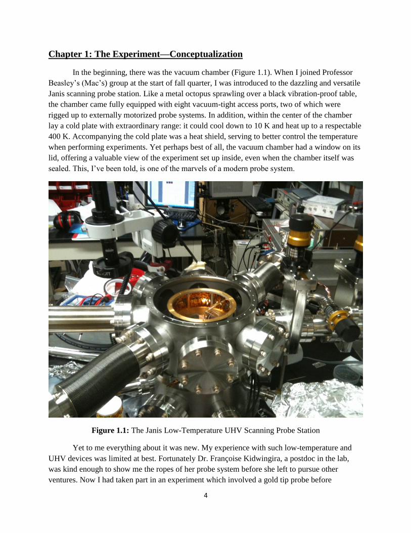
In the beginning, there was the vacuum chamber (Figure 1.1). When I joined Professor
Beasley’s (Mac’s) group at the start of fall quarter, I was introduced to the dazzling and versatile
Janis scanning probe station. Like a metal octopus sprawling over a black vibration-proof table,
the chamber came fully equipped with eight vacuum-tight access ports, two of which were
rigged up to externally motorized probe systems. In addition, within the center of the chamber
lay a cold plate with extraordinary range: it could cool down to 10 K and heat up to a respectable
400 K. Accompanying the cold plate was a heat shield, serving to better control the temperature
when performing experiments. Yet perhaps best of all, the vacuum chamber had a window on its
lid, offering a valuable view of the experiment set up inside, even when the chamber itself was
sealed. This, I’ve been told, is one of the marvels of a modern probe system.
Figure 1.1: The Janis Low-Temperature UHV Scanning Probe Station
Yet to me everything about it was new. My experience with such low-temperature and
UHV devices was limited at best. Fortunately Dr. Françoise Kidwingira, a postdoc in the lab,
was kind enough to show me the ropes of her probe system before she left to pursue other
ventures. Now I had taken part in an experiment which involved a gold tip probe before

5
embarking on this adventure, and I was expecting something of the same form. However, the tip
she was using was of a much different breed (Figure 1.2). The probe (in the form of a chip) had a
series of 4 miniscule contacts at its most pointed end, barely visible to the naked eye. They were
designed to flex when touched to a surface, such that they would make better (and softer) contact
with a given sample. The probe was intended to make local 4-point resistance measurements
through the 4 closely-spaced contacts. While a very reasonable design for that purpose, I
couldn’t help but be bothered with the painstaking care it took to align the probe properly. As I
watched Dr. Kidwingira try several times to rotate the chip holder so that the probes would all
touch down evenly on the gold surface, I wondered if there might be a better way to handle such
fine adjustments. But at the time I watched, hoping to remember what I could about the proper
procedures.
Figure 1.2: The probe chip. The contacts are at the tip of the gold rectangle but are too small to
be seen in this image.
Then it happened—the first accident of this project occurred less than a week in. A
graduate student in the lab was using the probe station for an experiment, and the heater was
accidentally left to its own devices. As the heater drove the temperature of the chamber higher
and higher, Dr. Kidwingira’s probe, “my” probe, began to melt away. The probe’s chip holder
was not suited to handle such high temperatures, and by the time we found it, it was merely a
black puddle clinging to the inside of the chamber.
I was surprised at this, of course, but I was no stranger to having mishaps in the lab. I was
not too worried about it at the time. Instead I saw in that amorphous pile of plastic a great
opportunity. In my naiveté I thought I could make the chip holder better, more adaptable, more
like one of James Bond’s playthings than a real piece of lab equipment. All the concerns I had
when watching Dr. Kidwingira align the probe came flooding back to my mind. Now I had the

6
chance to do something about them. I had the chance, I believed, to do something
technologically impressive. With that glimmer in my eye, I turned over many an idea in my
head, considering how I could fit so much functionality in so tight a space.
If you’re going to dream, why not dream big? I wanted to put everything I could in that
probe head: automated control of pitch and yaw, an automated scanning system, an improved
spring system to ease the probe touchdown, a more symmetric layout weighted to help keep
appropriate orientation, etc. (Figure 1.3). Needless to say, I was living in a very far away world.
Yet I contend that the ideas themselves had merit. Rather I had neither the experience nor the
resources to take on such an engineering product.
Figure 1.3: Original plan for the new probe head.
The rotational controls I was particularly passionate about. The difficulty in aligning the
probe head seemed to me the greatest problem to address. What I hadn’t appreciated was the
great difficulty in making such an automated system. While quite feasible in air, this probe head
had to deal with ultra-high vacuum and ultra-low temperatures. Most (affordable) actuators and
motors aren’t rated for such taxing conditions. Even fewer were small enough to fit in the less

7
than spacious confines of the chamber. But I looked around, searching for something that might
work, and I eventually hit gold. One company, Attocube, offered a miniature piezo rotation stage
that fit the bill. I was overjoyed to see it. It even fit my original plan for the probe head (Figure
1.3). Yet, as I said, I had hit gold, and as gold should be, it was prohibitively expensive. After a
representative happily gave me the exorbitant price point, I politely said I would get back to him
and began to look for opportunities elsewhere. My brief encounter with rotation stages came
unceremoniously to an end. While I was at first dejected, I realized I could still realize some
limited rotational motion with a linear actuator and a spring, and my hopes rose high again
(Figure 1.4). By mounting the chip holder on a rotatable disk, the linear actuator could push
against the spoke, thus rotating the disk and the chip. The springs would then provide resistive
force and keep the system stable. I hoped that in its simplicity it would be doable.
Figure 1.4: Schematic design using linear actuators to provide rotational movement
But my quest for a workable linear actuator was not a simple one. After having perused
the far reaches of the internet, I stumbled upon a peculiar linear actuator, the Squiggle motor.
The datasheets claimed it could handle the UHV and low-temperature conditions, all at a decent
price. I called up the vendors at once and inquired about the product, only to find out that their
8
price was for their standard model only, and that their claims about the UHV and low-temp
capabilities were for custom models. I had to accept the fact that my dreams were a little too
ambitious (at least for the time being).
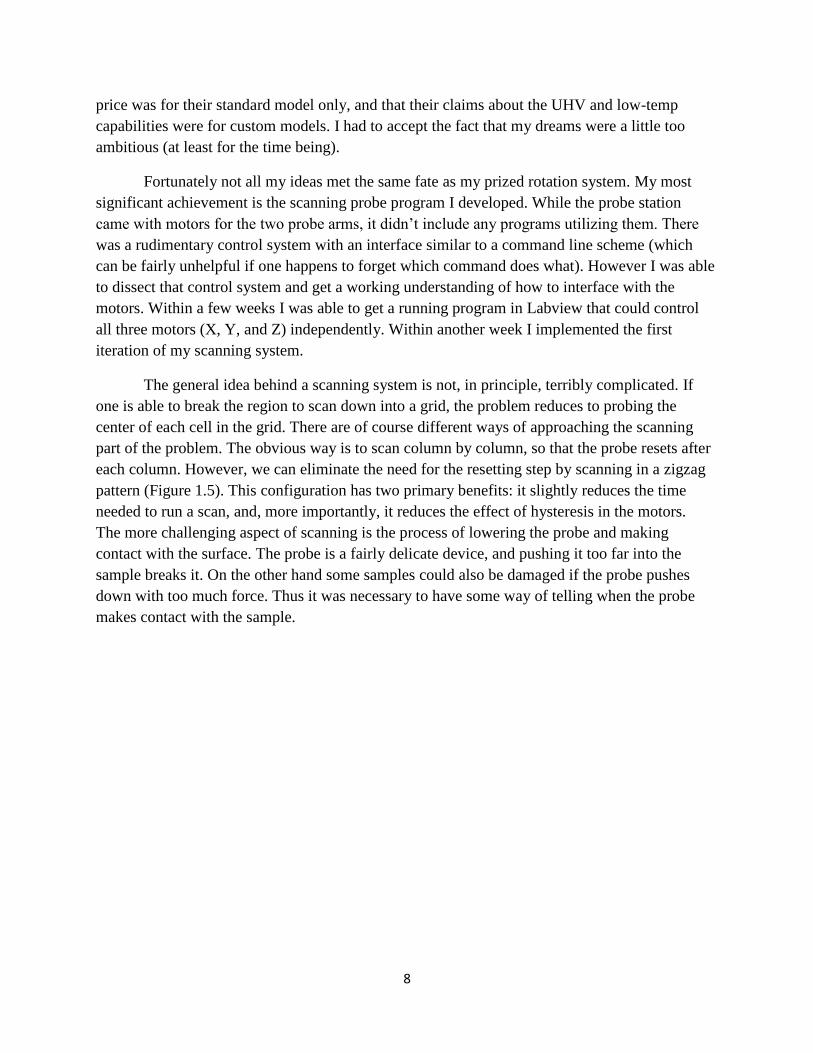
Fortunately not all my ideas met the same fate as my prized rotation system. My most
significant achievement is the scanning probe program I developed. While the probe station
came with motors for the two probe arms, it didn’t include any programs utilizing them. There
was a rudimentary control system with an interface similar to a command line scheme (which
can be fairly unhelpful if one happens to forget which command does what). However I was able
to dissect that control system and get a working understanding of how to interface with the
motors. Within a few weeks I was able to get a running program in Labview that could control
all three motors (X, Y, and Z) independently. Within another week I implemented the first
iteration of my scanning system.
The general idea behind a scanning system is not, in principle, terribly complicated. If
one is able to break the region to scan down into a grid, the problem reduces to probing the
center of each cell in the grid. There are of course different ways of approaching the scanning
part of the problem. The obvious way is to scan column by column, so that the probe resets after
each column. However, we can eliminate the need for the resetting step by scanning in a zigzag
pattern (Figure 1.5). This configuration has two primary benefits: it slightly reduces the time
needed to run a scan, and, more importantly, it reduces the effect of hysteresis in the motors.
The more challenging aspect of scanning is the process of lowering the probe and making
contact with the surface. The probe is a fairly delicate device, and pushing it too far into the
sample breaks it. On the other hand some samples could also be damaged if the probe pushes
down with too much force. Thus it was necessary to have some way of telling when the probe
makes contact with the sample.

9
Figure 1.5: The scanning potentiometer scans over the surface of the sample in a zigzag pattern
to save time and reduce the possible effects of hysteresis.
There were several techniques to consider in this regard, some more easily implemented
than others. Let us briefly describe a few of the methods considered.
Distance Method: For a reasonably flat sample, it is possible to keep track of how far
above the sample the probe is at all times. Then at each point on the grid (i.e. as in Figure
1.5), the probe is lowered by that distance, the measurement taken, and then the probe is
raised again so that it can be moved to the next point. There are some obvious
shortcomings to this method. For a non-uniform surface (or even if its plane does not lie
in the plane of the cold plate), this method fails to distinguish between points of different
heights, which means that it could potentially ruin the tip or sample in the process of
scanning. However it should be said that this measurement could be done in a more
sophisticated way. If one were able to measure the distance to the surface at each point,
say using a laser system attached to the probe, then this method could use that
information to make an adaptive scanning system. Of course this idea is again a little too
far into the clouds, and, while it would be nice to have, is not easily constructed in
practice. In any case, there are better alternatives to this method.
10
Capacitive Sensing: Capacitive sensing is an increasingly popular technology and would
theoretically fine for our system. Nevertheless it would be one of the more difficult
techniques to apply given the need for appropriate calibration. However this is definitely
a technology to consider for any further endeavors in this vein.
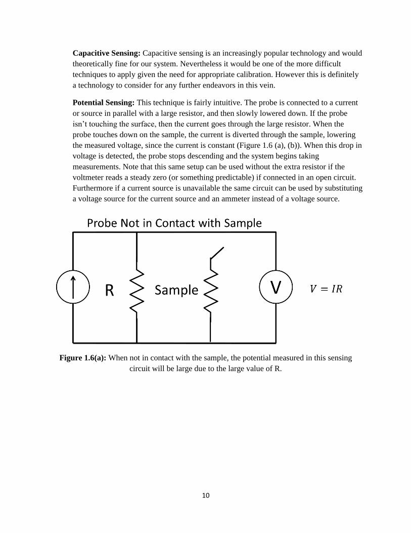
Potential Sensing: This technique is fairly intuitive. The probe is connected to a current
or source in parallel with a large resistor, and then slowly lowered down. If the probe
isn’t touching the surface, then the current goes through the large resistor. When the
probe touches down on the sample, the current is diverted through the sample, lowering
the measured voltage, since the current is constant (Figure 1.6 (a), (b)). When this drop in
voltage is detected, the probe stops descending and the system begins taking
measurements. Note that this same setup can be used without the extra resistor if the
voltmeter reads a steady zero (or something predictable) if connected in an open circuit.
Furthermore if a current source is unavailable the same circuit can be used by substituting
a voltage source for the current source and an ammeter instead of a voltage source.
Figure 1.6(a): When not in contact with the sample, the potential measured in this sensing
circuit will be large due to the large value of R.

11
Figure 1.6(b): When the probe makes contact with the sample, the measured potential drops
significantly since is chosen such that .
Of course, at this point, I didn’t yet know what exactly I was going to measure. I had
developed the scanning potentiometry system, but lacked something to try it on. Fortunately, that
was soon to come. In the first few weeks of winter quarter, I found my topic: Topological
Insulators.

12
Chapter 2: A Brief Overview of Topological Insulators
Given the fact that the focus of this project is on the properties of topological insulators,
it is only fitting that we discuss them in a little more detail. Of course, as mentioned in the
introduction, our methodology is largely based on the physical characteristics of topological
insulators. Nevertheless, there is much to be gained by getting a glimpse of the theory behind
their phenomenology (and their name). Of course, that being said, there is no middle ground in
this topic: one can either be very brief or very thorough. Since I have no intention of playing the
part of a theorist here, I opt for the former.
Recall for a moment the basic band gap model of the electron states in a material. An
insulating material is characterized by a band gap between the highest occupied states in the
valence band and the empty states in the conduction band. This model itself comes by treating
the material as an infinite periodic lattice, essentially assuming each atom is under the same
conditions as every other atom. However in reality materials are finite: there’s an edge
somewhere. In this sense we might wonder whether or not some phenomena occur at the
boundary of the material given this difference in symmetry in these regions.
As it turns out, in some cases the Hamiltonian describing the material is of the right form
so as to produce novel effects in those regions. In these surface regions the band structure looks
quite different from the band structure in the interior. While the electrons are confined to the
valence band in the insulating interior, the different boundary conditions at the surface allow for
the emergence of certain topologically-protected surface states, which can be occupied. These
states are topologically protected in the sense that their spin is locked to their momentum, such
that transitions between the states are reduced. Since the spins are locked to opposite momenta,
this means that the transitions from one topologically protected state to another take the form of
scattering phenomena. Thus with scattering heavily reduced, the electrons in these topologically
protected states can move about at the surface much as they would in a metal. This gives rise to
the statement that topological insulators have an exterior conductive surface and an insulating
bulk.
While the electrons in these topologically protected states exhibit other very interesting
properties (they are theorized to move about in a massless manner), we will be content with
considering only these conductive properties. There is a plethora of theoretical papers at the
moment as topological insulators continue to take hold of the condensed matter world, and the
field is continually evolving. In any case, much of this discussion above draws heavily on the
work of Fu and Kane, whose pioneering paper on TIs opened the way for this investigation [1].
13
Chapter 3: Simulating the Potential on the Surface of a Topological Insulator
Weigang’s idea, as aforementioned, was the type of statement that agreed well with
intuition. Of course, whereas my mind was quite satisfied by the claim that changing the interior
structure of a conductor would change the potential on its surface, I knew that a gut feeling
would be insufficient in such a project as this. More importantly, it is vital to run simulations to
model the potential on the surface of a topological insulator and for a normal conductor to check
that there actually is a significant difference between the two. After all, it would be entirely
possible that there would be differences of such small magnitude as to be practically
indistinguishable. Indeed if that were the case, then our attempt to probe the inner structure using
scanning potentiometry would be doomed to fail from the very beginning! Thus to allay these
concerns and provide a numerical background for our study, we proceed to investigate our
simulations of the potential on the surface of these two classes of materials.
As mentioned in our short theoretical digression, topological insulators owe their novel
properties to “topologically protected surface states”, a fact which, while theoretically
illuminating, is not a revelation that lends well to the task of simulation. However if we revisit
the basics of conduction in solids, we can make a large amount of headway. By focusing on the
primary physical characteristic of topological insulators—the insulating bulk and conductive
surface—we can show that significant differences arise between the potential on the surface of a
topological insulator and a normal conductor. In addition we will see that these differences are
dependent on the experimental setup, which allows for some optimization on the part of the
experimentalist.
Modeling the Electric Potential in a Conductor with Laplace’s Equation:
Let us revisit one of the most basic models of conduction in homogenous solids—Ohm’s
Law. In the following discussion, the variables are labeled following standard convention: is
the current density in the material, the corresponding electric field, and the conductivity of
the material, which in general is spatially dependent.
Assumption 1:
Justification: This is merely a general formulation of Ohm’s Law, an equation familiar
to anyone who has had the slightest exposure to circuits. It reduces to the more familiar
form in the case of a homogenous material (where is constant). In any case, this
is a standard model of conduction in solids and is an appropriate starting point for our
investigation.
Assumption 2:
Justification: This is a statement of current continuity in the material. That is, there
should be no “sources” or “sinks” in the interior. In essence, this reflects the fact that we
14
expect to have only one such source and sink in the system, in the form of the voltage
source or current source in our experimental setup. It is almost inconceivable that this
would break down in our experiment.
Assumption 3: uniform
Justification: This assumption might be considered the most suspect of the three. It is not
uncommon for materials to have non-uniform conductance, and in more careful studies is
something to be considered. It is interesting to note, however, that certain simple
anisotropies (say having different conductances along different axes) can be handled by a
change in variables along the respective dimensions. In this sense we can modify our
models to suit a fairly diverse class of materials, though more exotic conductances will
inevitably require more sophisticated simulations.
Working off of these three assumptions, we can take the divergence of Ohm’s Law to find
( )
( )
Then since
We have that
Finally, given that the conductance is constant, it follows that
Hence the potential distribution in an Ohmic material under the above assumptions satisfies
Laplace’s equation.
We can thus model the potential in a normal conductor as a solution of Laplace’s
equation. Of course we have not yet spoken of the boundary conditions, which determine the
unique solution to Laplace’s equation. These boundary conditions take the form of mixed
Dirichlet (fixed value) and Neumann (fixed derivative) conditions. Thus, for any point on the
surface of the material, either the potential is fixed, or its derivative is fixed (in this case 0). Of
course it is possible to have the more general Robin type condition (which is a condition on both
the value and derivative of the potential at the surface), but our experiment should not introduce

15
a need for such conditions. Now how do we interpret these boundary conditions experimentally?
Let us discuss this in a little detail:
Dirichlet Conditions: The fixed-potential condition has a very intuitive meaning.
Essentially those points on the surface with fixed potential are those points directly
connected to the voltage or current source (for DC current). Note that we must be more
careful with this condition if we use an AC source, but in such a case we must also be
careful about using Laplace’s equation, as we introduce time dependence in the system.
While it would be an interesting extension to work with AC sources, in this case
experiment we deal only with DC sources, and hence we assume this for the following
discussion.
Neumann Conditions: It would be very strange if we had current streaming out of the
material (not to mention unphysical), so this is something we must prevent by applying
appropriate boundary conditions. Recall that the electric field is proportional to the
derivative of the potential, and the electric field is what drives currents. Hence if we don’t
want current to stream off the material, we want no electric field perpendicular to the
surface of the material, and thus we want the derivative of the potential to be zero
perpendicular to the surface.
Recall that the boundary conditions are mixed; that is, we have both Dirichlet and Neumann
conditions on the surface in different regions. Wherever the potential isn’t set, we have the
Neumann condition instead. Of course, the experimentalist has free reign (practicalities aside)
over where to set the potential by choosing where to connect the material to the voltage/current
source, and by choosing how to connect (i.e. by wire bonding, epoxy, etc.). Figure 3.1 provides a
visual representation of our discussion of the boundary conditions on a normal conductor.
Figure 3.1: Demonstration of the location of Dirichlet and Neumann boundary conditions on the
exterior surface of a material.

16
Modeling the Electric Potential in Topological Insulators with Laplace’s Equation:
Having developed our model for normal conductors, we can attempt to apply the same
procedure to topological insulators. Assume for now that the conductive layer of the topological
insulator at hand obeys Laplace’s equation. That is, we assume that conduction in the topological
insulator (where it is conductive) is the same type of conductance seen in a normal conductor.
All we are assuming is that the conductance is Ohmic, which is a natural assumption to make. So
how then do we distinguish the model of a topological insulator from a model of a normal
conductor? The key, as is always the case with Laplace’s equation, is in the boundary conditions.
Recall that the defining physical feature of a topological insulator is its insulating bulk. It
goes without saying that this insulating interior must factor into the simulation in some form. The
only question is how to do it. The natural way to approach the problem is to follow the same type
of reasoning we did before. The insulating bulk of the topological insulator should have very
little current flowing through it since the surface layer is far more conductive. If we dare to
anthropomorphize the current for a minute, “the current wants to go the easy way around and
avoid the insulator”, as shown in Figure 3.2. Now this reminds us of a similar situation on the
boundary of the normal conductor. We wanted no current to flow off of the material into its
surroundings, and in this case we want no current to flow off of the conductive layer into the
interior. How were we able to account for this? Neumann boundary conditions! If we add
Neumann boundary conditions on the boundary between the conductive layer and the insulating
bulk, we effectively prevent current from flowing into the interior of the topological insulator,
simulating the effect of the insulating bulk.
Figure 3.2: Schematic of differences in current path between a normal conductor and a
topological insulator.

17
The only difference in our simulations of the potential in a normal conductor versus our
simulations in a topological insulator is the presence of this interior Neumann boundary. More
explicitly, the simulations for a normal conductor are solutions of Laplace’s equation with the
given external boundary conditions in a solid material, whereas for a topological insulator the
simulations are solutions of Laplace’s equation with the same external boundary conditions in a
conductive shell. Thus what we intend to compare is the difference in the potential on the surface
due only to the presence of the insulating bulk.
It should be noted, however, that this model may be inadequate to describe completely
the actual phenomenology of a topological insulator. Yet progress is a gradual thing. Our intent
is, in short, to see how well this simple model fares in an actual experiment. If what we see
supports our model, fine; if not, we make modifications where necessary. As the old saying goes,
“a journey of a thousand miles begins with a single step”. Let us now make that step.
Scale Invariance and Other Properties of Solutions of Laplace’s Equation:
Laplace’s equation is mathematically a very beautiful equation. Its simplicity and
geometric nature bestow it with several properties that serve us well in both simulations and in
experiments, the most important of which are its scale invariance and the mean value property.
These properties (among others) are explored in any textbook on partial differential equations or
harmonic functions, and it will be beneficial to look into them here as well.
Scale Invariance: The concept of scale invariance is a concept of symmetry; in fact it is
one particularly popular among theorists. And for good reason too, as scale invariance is
a very useful quality to have in a system. Pertaining to this particular case, Laplace’s
equation is Scale Invariant in the sense that a uniform scaling of spatial dimensions
leaves the equation unchanged. That is, for any scaling transformation of the form
Where is a nonzero constant, we have the same equation in the new variables as we did
in the old. This follows from an application of the chain rule:
18
However this is not the full extent of the scale invariance of Laplace’s equation. By a
similar argument as above, any rescaling of the potential leaves the equation invariant as
the left hand side is zero. This is quite useful in practice, as it permits the use of arbitrary
units. Thus we need only be concerned with where we set the potential to be fixed, not
with the actual values we set there. Then to get the potential for any set of boundary
conditions with the same geometry, we simply scale the potential. Note that the relative
values of the fixed potentials cannot be changed in this manner. For example, if one had
three wires at three different potentials contacting the material, any scaling would
preserve their relative order. Fortunately in our case we only consider systems with two
fixed values, so any potential can be obtained by scaling.
Mean Value Property: The second important property of Laplace’s equation is
significant because of the stability it affords to numerical techniques. Solutions to
Laplace’s equation have the remarkable property that the value of the solution at any
point is equal to the average value of the solution on any sphere centered around
contained within the boundaries of the region. In mathematical notation, let be the
region in which the solution is defined. Then for all , and all such
that , we have
(
)∫
As any background in analysis reveals, the limit of the sequence of averages of a
sequence is often better behaved than the limit of the sequence itself. In fact there are
cases when the average sequence converges even though the parent sequence does not
(for example the oscillating sequence 1,-1,1,-1,…). We will heavily exploit this property
to numerically solve Laplace’s equation, as it not only suggests a way to solve the
equation (by iteratively taking averages), but also guarantees the convergence and
stability of such numerical solutions.
These are by no means the only significant properties of Laplace’s equation, but the
others, while insightful, don’t bring much to the table in this situation. For instance, a solution to
Laplace’s equation takes its minimum and maximum values on its boundary. This can be helpful
in testing to see if a program is returning reasonable results, but this doesn’t play as key a role as
the previous two properties. Furthermore Laplace’s equation is a Sturm-Liouville operator,
which affords it many nice qualities, chief among which is the fact that its eigenfunctions are
complete in the norm. For example, the eigenfunctions of a rectangular solid are simply the
basis vectors in the three-dimensional Fourier series. While this is a profound result and
important in a theoretical sense, it is nontrivial to solve for the eigenfunctions in the case of the
topological insulator due to the fact that the model is a shell instead of a solid. For any more
complicated geometry the eigenfunctions are likely to be even more complex! In any case, the
19
numerical solutions we perform don’t rely on finding a complete orthonormal sequence of
eigenfunctions, so we will not pursue the matter further at this point.
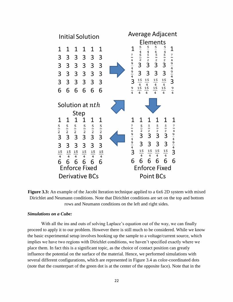
Numerically Solving Laplace’s Equation Using Jacobi Iteration:
The Mean Value Property suggests a very direct way of computing the solution to
Laplace’s Equation with given boundary conditions. Discretize the region, make a guess as to
what the potential should be everywhere, and then take averages and enforce boundary
conditions. Lather, rinse, and repeat. This is the technique of Jacobi Iteration, sometimes known
as the Relaxation Technique. There is a satisfying simplicity in this method—it not only makes
the algorithm easy to comprehend, but also easy to implement for relatively nice regions. Of
course things can get hairy if we choose to model vary strangely shaped materials, but such
situations are not outside of the realm of possibility. Note however that more complicated
regions would be better handled with more specialized techniques, such as the finite element
method, which take care to sample the region in such a way that critical parts are given more
attention. Let us investigate the workings of Jacobi Iteration further.
Discretization: Computers are, by nature, discrete things, and any numerical technique
must therefore involve some degree of discretization. This occurs in two ways when
solving Laplace’s Equation. First, the region in which the equation is to be solved must
be discretized, that is, reduced to a lattice of points on which the discrete solution is
defined. Second, the equation itself must be discretized to conform to this discretized
region.
Discretization of the Region: It would be convenient if we could perform
computations on a continuous domain, but computers can’t handle infinite
numbers of points, so we settle for less. Recall from our earlier discussion of scale
invariance that only relative distances matter, hence it is the geometry of the
region that is important. By choosing our mesh size (i.e. how many cells into
which we divide the region), we directly control the accuracy of the simulation.
Note that, for more complicated regions this discretization step must be handled
with care, as certain subregions might require a tighter mesh than others, in which
case the finite element method is the best choice for simulation.
Discretized Laplace’s Equation: The natural analog of taking the derivative at a
point in a continuous domain is to take the difference between two points in a
discrete one. Thus, without loss of generality, the derivative in the x direction
becomes

20
where is the distance between points in the direction. We follow a similar
procedure to obtain the second derivative (which is just the derivative of the first
derivative). However there is one ambiguity to consider in the discrete case. We
can choose to take the second derivative by taking the derivative again at the
point , or we can take the centered second derivative,
By extension, we also have
Now assume our lattice is uniform, , and relabel the point
with the indices , (i.e. ). Then we have
Notice that is merely a restatement of the Mean Value property! We have that the
potential at any point on the lattice is given by the average of the potential at
adjacent points. We could have guessed this relation without going through the
discretization process, but we now have it on firmer mathematical ground.
Initialization: In Jacobi iteration it is necessary to have an initial guess as to what the
potential should be. In theory the guess doesn’t matter; the algorithm should still
converge to the appropriate solution. However in practice a wise initial choice greatly
increases the convergence, which saves valuable computation time. In our case, we will
always have one region set to be fixed at a value of 100, with another fixed to 0, and so as
an initial guess we take the interior to be the average, 50. For more complicated systems
it can speed up computations considerably to take initialization into more consideration.
Iteration: The iterative step begins with averaging each of the elements according to the
discretized Laplace’s equation. This effectively disrupts the boundary conditions, and so
they must be reinstated after averaging.
Dirichlet Conditions: The Dirichlet (fixed-point) boundary conditions are quite
easy to enforce. After performing the averaging step, we need only set the
potential at those fixed points to the appropriate value.

21
Neumann Conditions: In contrast to the Dirichlet boundary conditions, it is a
little more difficult to enforce Neumann conditions. However it is not an
intractable problem. By setting the boundary cells to be equal to their adjacent
cells, we have zero derivative perpendicular to the boundary. This is convenient
for our simulations because the regions we are working with are rectilinear, so
“adjacent” is well defined. On the other hand, if we wished to run a simulation on
a sphere, we would have to adapt to the fact that the derivative must be zero in the
radial direction, which is more difficult to handle in this discretization scheme.
Again, for such cases it would be beneficial to switch to an alternate technique
which more carefully generates the mesh.
After averaging and enforcing boundary conditions, we check to see if the maximum
difference between the current iteration and the previous is under a certain limit, which
we call . We stop iterating when the maximum difference is below More explicitly,
the simulation ends at the th iteration, when
Having worked through the details, Figure 3.3 provides a concrete example in a two-dimensional
setting. Note that Dirichlet conditions are being enforced on the top two rows and Neumann
conditions on the left and right sides.
22
Figure 3.3: An example of the Jacobi Iteration technique applied to a 6x6 2D system with mixed
Dirichlet and Neumann conditions. Note that Dirichlet conditions are set on the top and bottom
rows and Neumann conditions on the left and right sides.
Simulations on a Cube:
With all the ins and outs of solving Laplace’s equation out of the way, we can finally
proceed to apply it to our problem. However there is still much to be considered. While we know
the basic experimental setup involves hooking up the sample to a voltage/current source, which
implies we have two regions with Dirichlet conditions, we haven’t specified exactly where we
place them. In fact this is a significant topic, as the choice of contact position can greatly
influence the potential on the surface of the material. Hence, we performed simulations with
several different configurations, which are represented in Figure 3.4 as color-coordinated dots
(note that the counterpart of the green dot is at the center of the opposite face). Note that in the

23
following simulations we take advantage of the scale invariance of Laplace’s equation and so use
arbitrary units for the axes and potential.
Figure 3.4: Contact points for our simulations of Laplace’s Equation on a cube. The
corresponding green dot is located on the center of the opposite face.
Contacts on One Surface of the Cube: This case represents a natural experimental
setup since it is often easiest to place the electrical contacts on the top face of the material
under test. However we don’t expect the difference between the potential on the surface
between a normal conductor and a topological insulator to be as dramatic as it could be
since the contacts are on the same face. That is, the presence of the insulating bulk does
not change the primary current path between the two contacts.
Figure 3.5(a): The following simulations model the potential on the yellow surface.
The normal case simulation (Figure 3.5(b)) displays sensible characteristics. Note
that the square regions in the two corners represent the wires connecting the sample to the
voltage/current source. We see a slowly varying gradient going across in the x direction
as the current flows from one contact to the other. We don’t see the uniform gradient
expected in a 2D conductor because the current is able to spread out throughout the
interior of the sample. In any case, this simulation has the most value when compared to
the topological case, which we have below.
24
Figure 3.5(b): Potential on the surface of a normal conductor.
Figure 3.5(c): Potential on the surface of a topological insulator.

25
Our simulation for the potential on the surface of a topological insulator (Figure
3.5(c)) displays some very interesting differences from the normal case. Note that the
positions of the contacts are the same; the external boundary conditions are unchanged.
However, the potential differs in magnitude as well as distribution. The potential falls
quickly away from the contacts in the normal case, reflecting the fact that current is
flowing throughout the interior of the cube. On the other hand, the gradient in potential is
much more gradual in the topological insulator case, which reflects the fact that the
current is essentially being forced to flow closer to the surface of the material.
This simulation is promising in that even this non-ideal case would seem to
display significant differences between the normal and topological states. It also
highlights the important feature that the difference between the potential in the normal
and TI case is not a uniform offset, but a spatial difference. The fact that we can use the
spatial pattern of the potential on the surface is an enormous asset. But let us continue
with the next case before discussing this further.
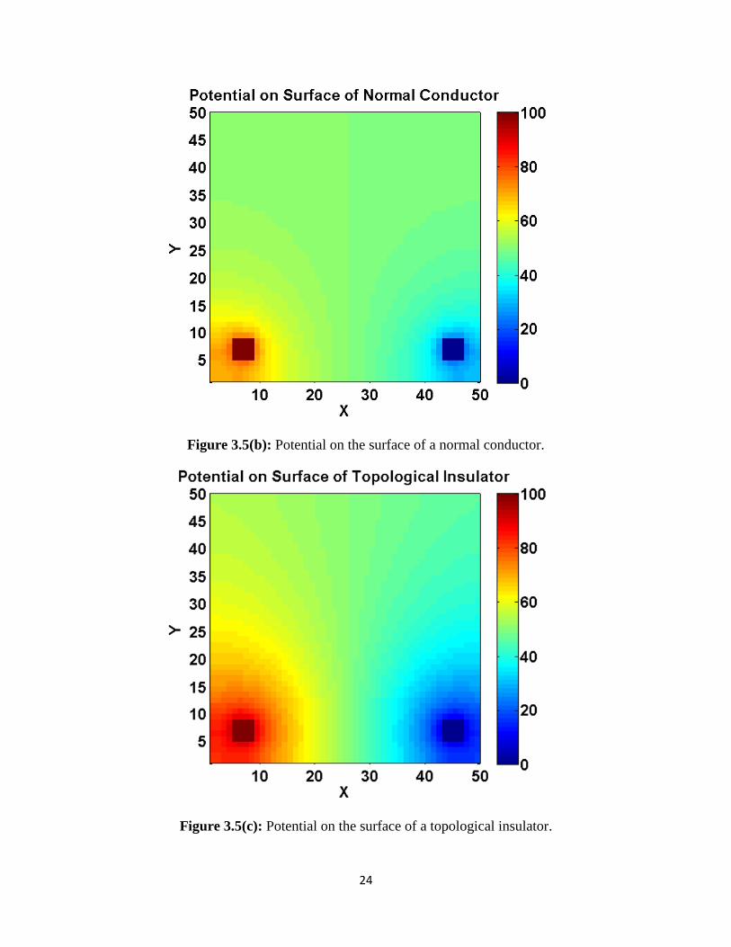
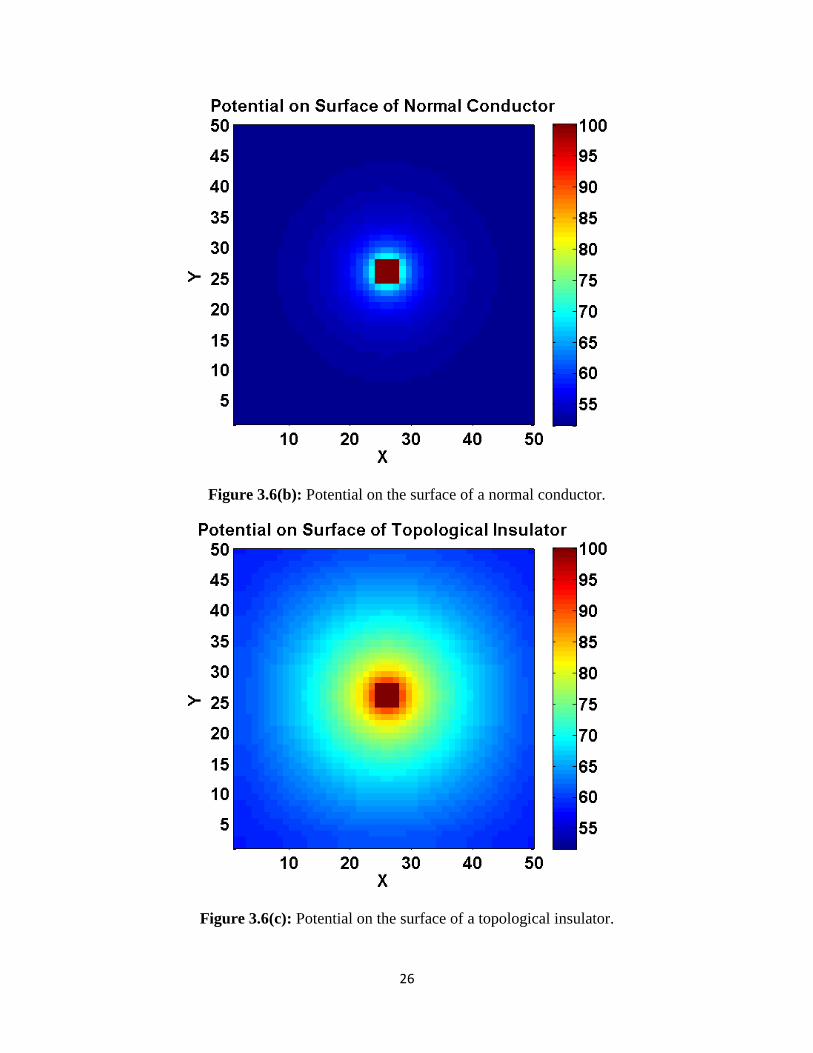
Contacts on Opposite Faces: This contact configuration would intuitively seem to be
one of the best for displaying differences between normal materials and topological
insulators. In a normal material, the majority of the current would flow through the center
of the material, something which is forbidden by a topological insulator. With that
reasoning in mind, we attempted a simulation of this configuration with beautiful results.
We will only show the simulation on the yellow face here. Though there are also
significant differences in the potential on the remaining orange faces, the differences still
are not as pronounced as the differences on the faces with the contacts.
Figure 3.6(a): The following simulations model the potential on the yellow surface.
26
Figure 3.6(b): Potential on the surface of a normal conductor.
Figure 3.6(c): Potential on the surface of a topological insulator.
27
The vast difference between the topologically insulating and normal materials is
evident as soon as one looks at the two images. The picture depicts our intuition in action.
In the normal case, the potential is nearly constant towards the edges, which of course
implies that the gradient of the potential is close to zero at those points, and hence that
little current is flowing through that part of the surface. Indeed it appears that the current
is working its way through the conductor by traveling through its interior.
In stark contrast, the potential on the surface of the topological insulator gradually
falls from the center, marking the path of the current flowing around the insulating bulk
to get to the contact on the other side. Note that there is a symmetry in the system which
is not quite rotational due to the fact that the region is a square, but otherwise the
potential displays this square symmetry.
Once again, this spatial difference, which here is quite prominent, aids us greatly
in our attempt to identify and characterize topological insulators.
Simulations on a Wafer:
The simulations on a cube were a nice starting point given its nice symmetries. However,
real samples don’t always come in cubes. Indeed, our own sample TI was shaped more like a
rectangular wafer—a thin piece of material with rectangular surfaces. This was at first quite
worrisome, as we thought that the thinness of the material would reduce what differences we
would see. Thus, to test whether or not this shape would prevent us from finding useful data, we
ran more simulations with this geometry. Note that the following simulations are carried out on
an object 92 by 92 by 16 pixels in dimension.
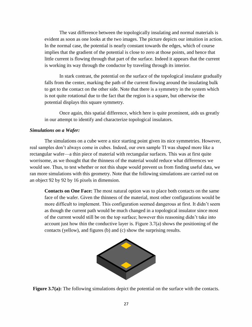
Contacts on One Face: The most natural option was to place both contacts on the same
face of the wafer. Given the thinness of the material, most other configurations would be
more difficult to implement. This configuration seemed dangerous at first. It didn’t seem
as though the current path would be much changed in a topological insulator since most
of the current would still be on the top surface; however this reasoning didn’t take into
account just how thin the conductive layer is. Figure 3.7(a) shows the positioning of the
contacts (yellow), and figures (b) and (c) show the surprising results.
Figure 3.7(a): The following simulations depict the potential on the surface with the contacts.
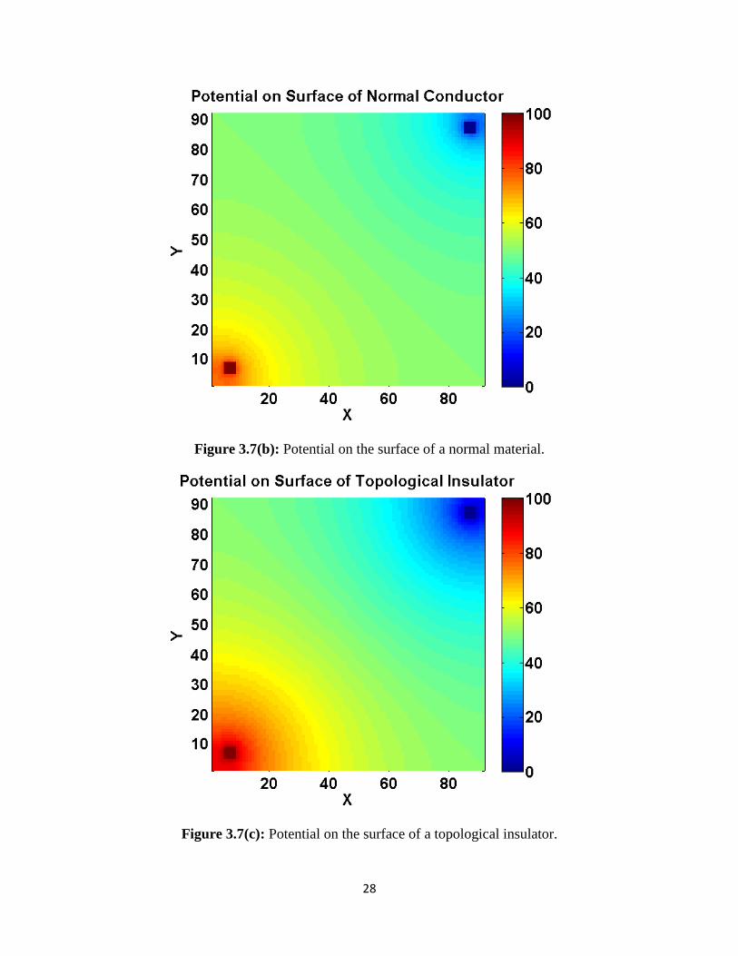
28
Figure 3.7(b): Potential on the surface of a normal material.
Figure 3.7(c): Potential on the surface of a topological insulator.

29
Fortunately the simulations showed that our concerns weren’t too much of a problem.
There is again a spatial difference in the potential, though somewhat slighter than what
we had seen in the analogous case for the cube. As usual, the gradient in potential is more
pronounced in the case of the topological insulator, reflecting the fact that more current
travels close to the surface.
We are beginning to see here a categorical difference between the potential on the
surface of normal materials and topological insulators. The decrease in potential as one
moves away from one contact tends to drop more quickly for a normal material than for a
topological insulator due to the diversion of current to the interior. This recurring
phenomenon is a good sign that we might have a nice way of indicating if our real data
looks appropriate.
Now even though this simulation showed resolvable differences, we thought we
could do better. We posited that attaching one surface to a ground plane and then placing
one contact on the opposite surface would result in an even greater difference.
Contact on Top and Ground Plane: In theory we thought it would be best to have the
ground plane only touch the bottom of the sample, but in practice it turned out that the
sides were accidentally attached to the ground plane as well. As it turns out, this change
in configuration, while seemingly significant, had a negligible effect on the potential on
the surface. Figure 3.8(a) shows a schematic of the contact configuration.
Figure 3.8(a): The following simulations depict the potential on the surface of the dark gray
region (labeled as to reflect the species of the actual sample).

30
Figure 3.8(b): Potential on the surface of a normal material.
Figure 3.8(c): Potential on the surface of a topological insulator.

31
The difference we see here between the normal and topologically insulating materials is
the most significant yet! Furthermore we see the same type of pattern we mentioned: the
potential drops off more quickly in the normal material than in the topological insulator.
This was a highly encouraging result, as what we had feared might be an insurmountable
problem turned into a considerable asset. By exploiting the geometry of the situation we
could make much more useful measurements. After seeing this simulation, I hurried to
prepare the sample of Bismuth Selenide in this configuration. Unfortunately I soon
realized that real materials aren’t as easy to deal with as computer simulations.
Identifying and Characterizing Topological Insulators:
Before moving on to the experimental side of things, it would be best to discuss here how
we could interpret our data to identify and characterize topological insulators. The main idea,
which should seem obvious, was to compare the data to the simulations. By capitalizing on the
spatial distribution of potential on the surface, we could make meaningful comparisons between
simulations and data. In addition, for any sample under test, it would be possible to make a
sample of the same shape and size out of a normal material, with which a control test could be
performed. Then one could directly compare the data from a normal and presumably topological
sample. This would again take advantage of the scale invariance of Laplace’s equation to remove
any problems with the scaling of the potential or differences in the resistance of the two samples.
Of course this still leaves many questions unanswered. For one, can we be sure that
seeing the predicted signatures actually means that a material is a topological insulator? In
practice, one cannot always be so sure. We have made some assumptions as to the properties of
the materials we considered, and it is possible that some materials might have properties exotic
enough to mimic the potentials we would like to associate to topological insulators. Nonetheless,
we can still use the scanning potentiometry measurement to characterize topological insulators.
Having spatial data gives us a window into the conduction patterns on the surface and allows us
to look at any irregularities that might arise. Of course any technique requires some refinement
before it can be applied with full confidence, and this technique, still in its infancy, requires
extensive testing.
32
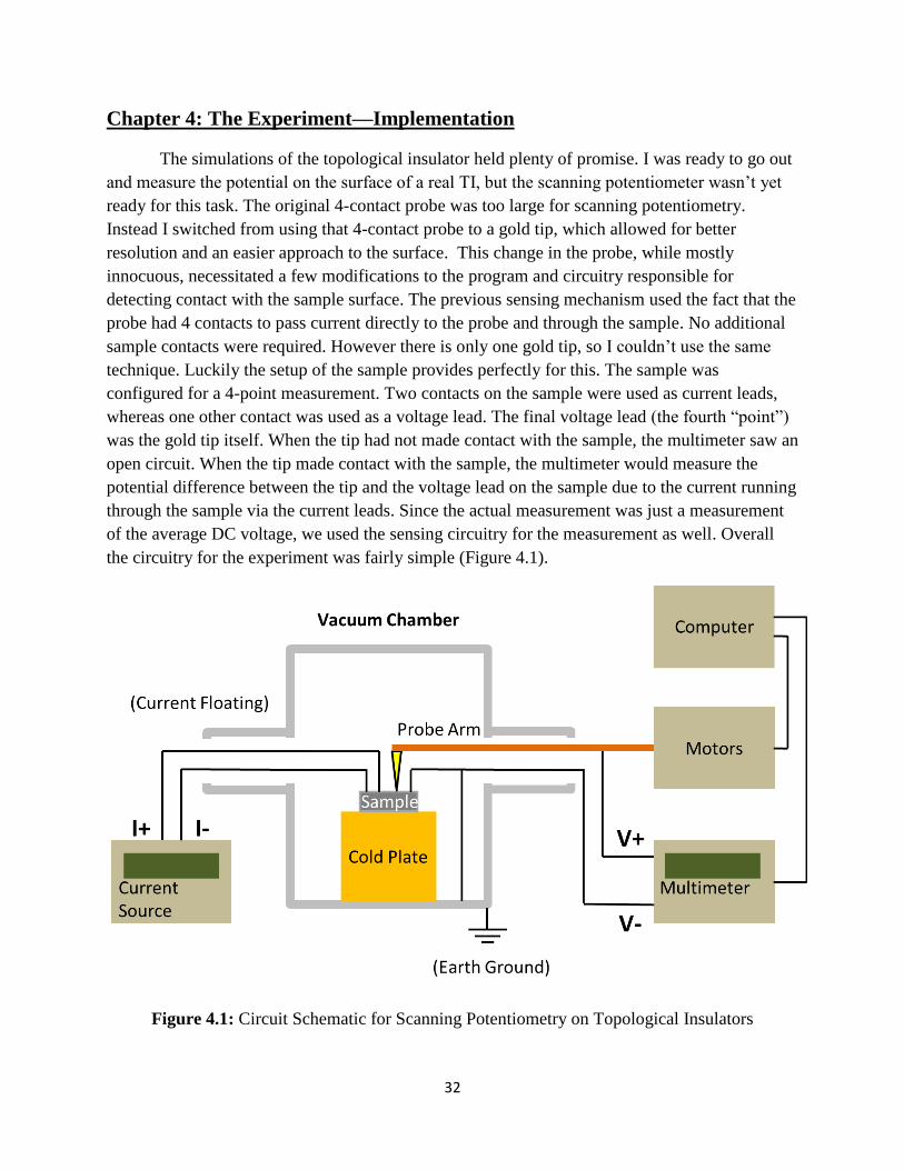
Chapter 4: The Experiment—Implementation
The simulations of the topological insulator held plenty of promise. I was ready to go out
and measure the potential on the surface of a real TI, but the scanning potentiometer wasn’t yet
ready for this task. The original 4-contact probe was too large for scanning potentiometry.
Instead I switched from using that 4-contact probe to a gold tip, which allowed for better
resolution and an easier approach to the surface. This change in the probe, while mostly
innocuous, necessitated a few modifications to the program and circuitry responsible for
detecting contact with the sample surface. The previous sensing mechanism used the fact that the
probe had 4 contacts to pass current directly to the probe and through the sample. No additional
sample contacts were required. However there is only one gold tip, so I couldn’t use the same
technique. Luckily the setup of the sample provides perfectly for this. The sample was
configured for a 4-point measurement. Two contacts on the sample were used as current leads,
whereas one other contact was used as a voltage lead. The final voltage lead (the fourth “point”)
was the gold tip itself. When the tip had not made contact with the sample, the multimeter saw an
open circuit. When the tip made contact with the sample, the multimeter would measure the
potential difference between the tip and the voltage lead on the sample due to the current running
through the sample via the current leads. Since the actual measurement was just a measurement
of the average DC voltage, we used the sensing circuitry for the measurement as well. Overall
the circuitry for the experiment was fairly simple (Figure 4.1).
Figure 4.1: Circuit Schematic for Scanning Potentiometry on Topological Insulators
33
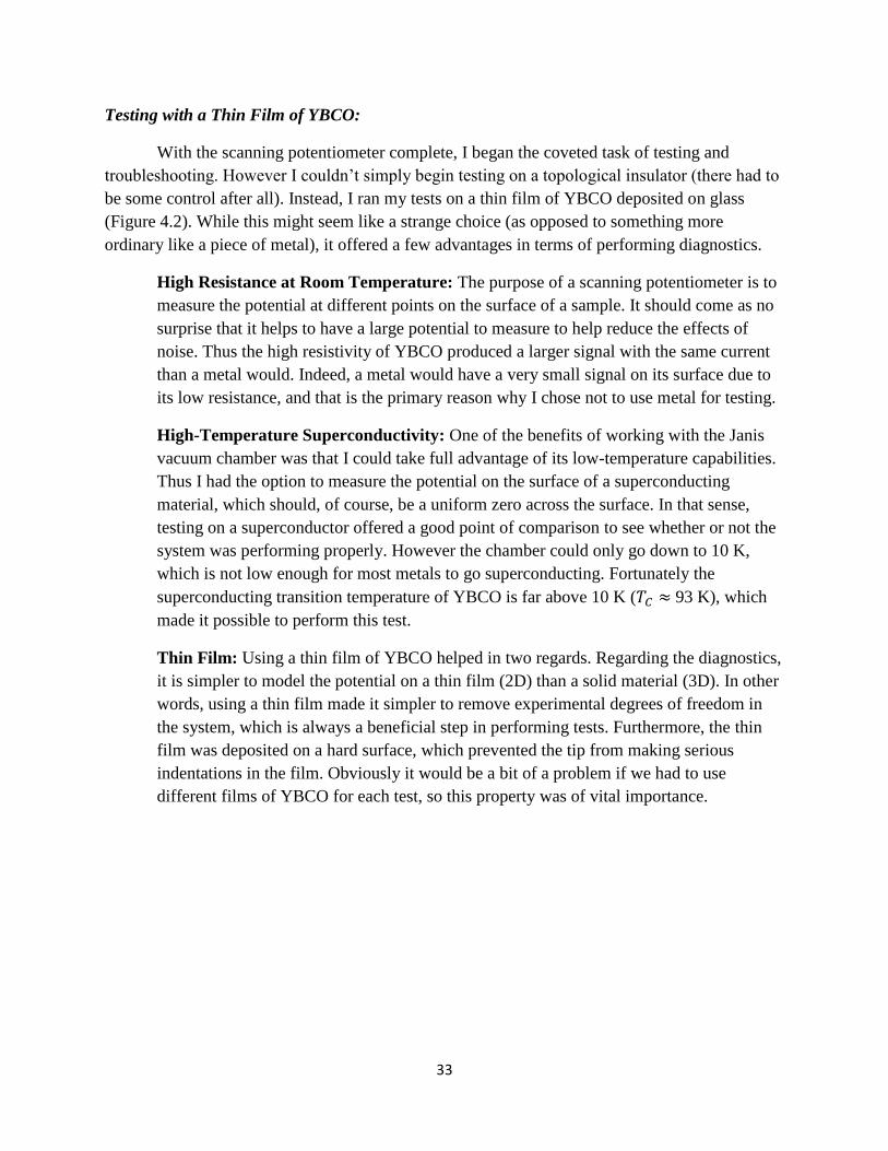
Testing with a Thin Film of YBCO:
With the scanning potentiometer complete, I began the coveted task of testing and
troubleshooting. However I couldn’t simply begin testing on a topological insulator (there had to
be some control after all). Instead, I ran my tests on a thin film of YBCO deposited on glass
(Figure 4.2). While this might seem like a strange choice (as opposed to something more
ordinary like a piece of metal), it offered a few advantages in terms of performing diagnostics.
High Resistance at Room Temperature: The purpose of a scanning potentiometer is to
measure the potential at different points on the surface of a sample. It should come as no
surprise that it helps to have a large potential to measure to help reduce the effects of
noise. Thus the high resistivity of YBCO produced a larger signal with the same current
than a metal would. Indeed, a metal would have a very small signal on its surface due to
its low resistance, and that is the primary reason why I chose not to use metal for testing.
High-Temperature Superconductivity: One of the benefits of working with the Janis
vacuum chamber was that I could take full advantage of its low-temperature capabilities.
Thus I had the option to measure the potential on the surface of a superconducting
material, which should, of course, be a uniform zero across the surface. In that sense,
testing on a superconductor offered a good point of comparison to see whether or not the
system was performing properly. However the chamber could only go down to 10 K,
which is not low enough for most metals to go superconducting. Fortunately the
superconducting transition temperature of YBCO is far above 10 K ( 93 K), which
made it possible to perform this test.
Thin Film: Using a thin film of YBCO helped in two regards. Regarding the diagnostics,
it is simpler to model the potential on a thin film (2D) than a solid material (3D). In other
words, using a thin film made it simpler to remove experimental degrees of freedom in
the system, which is always a beneficial step in performing tests. Furthermore, the thin
film was deposited on a hard surface, which prevented the tip from making serious
indentations in the film. Obviously it would be a bit of a problem if we had to use
different films of YBCO for each test, so this property was of vital importance.

34
Figure 4.2: Thin film of YBCO on glass mounted with varnish on copper plate. The metal pads
to the left were used to wire bond to the YBCO film.
With the thin film in hand (in gloves of course), I proceeded to prepare for the tests. The
first issue at hand was to place contacts on the surface of the YBCO. This was my first brush
with the wire bonder. If ever there were an antagonizing force in this project, it would have to be
that machine. At the time I hadn’t used it before, though I knew of its presence and its purpose. It
seemed simple enough to operate. Touch the wedge to start the bond, touch again to finish. But I
could never make it bond. I would try again and again, sometimes making one half of the bond,
but inevitably breaking the other. And the rethreading—I spent what seemed hours at a time
trying to rethread that wedge! It seemed, at times, absolutely hopeless.
Yet there was hope. My good friend, Katherine Luna, had the heart to help me with wire
bonding. As a grad student in the lab, she had accrued a great deal of experience in wire bonding.
I watched in wonder as she effortlessly made bond after bond, in awe of her skill and in
amazement at my ineptitude. As quickly as she started, she finished. What I had tried in vain to
do for hours, she did in seconds. Without her aid the experiment never could have progressed.
But that was not the end of her kindness. I varnished the YBCO holder to the cold plate
and was ready to seal the chamber and pump down to vacuum; only I didn’t know how to go
about doing that step. Fortunately Katherine once again stepped in with her advice. Showing me
how to properly prepare for vacuum, telling me how plastics would outgas and ruin vacuum,
reminding me not to use too much vacuum grease—she once again saved my project. After a few

35
times pumping down, I began to get the hang of things. I wasn’t perfect at it of course, (and I
might still use too much vacuum grease), but I was proficient enough at pumping down and
cooling down to run my tests.
But all did not work as planned. The chamber was evacuated, and the cold plate was
down to 10K. As I looked inside the chamber I could see the wire bonds still intact. Everything
was intact. I never expected it would be the motors! I had full confidence that my motor controls
worked as they were supposed to. They moved just as I had expected when I had tried them
before. What could possibly go wrong? Yet when I started scanning the YBCO I noticed
something was amiss. The probe was supposed to cover a rectangular region on the YBCO;
however it seemed to move off its given path. I watched first in curiosity. I was perplexed by this
development, though I was still getting contact, so I didn’t think much of it. But as it slowly
inched closer to the wire bonds, I began to get nervous. I’m not much of a gambling man, but
that day I took a risk—I let it run. Then, faster than I could react, the probe smashed a wire bond.
I stopped the program, but the damage was already done.
Fortunately there were 4 contacts on the YBCO, and I only needed 3 for the test.
Unfortunately, the one contact I wasn’t using didn’t work. The wire connecting it and the outside
world had broken inside the chamber. The first test was a logistic failure.
I racked my brain for quite some time trying to figure out what went wrong. If the
scanning system didn’t work then the whole project was dead! I wasn’t about to stand around
and manually move the probe over more than 100 points. But things didn’t seem to add up. It
worked perfectly the last time I had tried it! So I unsealed the chamber and tested it again. This
time it seemed to be working. At first this only confused me more, but I decided to give it
another go. Katherine helped me reattach the wire bonds and repair the broken wire, and I sealed
the chamber up once again. I clicked the start button, and I heard it immediately.
As Mac told me afterwards, “Now you know the force of 1 atmosphere!” I had not
thought about how the vacuum would make it more difficult to move the probe into and out of
the chamber (x direction), but it was clear that it was the culprit. After all such motion either
compressed or expanded the accordion arm connecting the probe to the chamber. Evidently the
action of expansion is much more difficult to do with the air against you. This was a difficulty I
could conquer. I changed the scanning program so that it scanned monotonically in the x
direction (it zigzagged in the y direction instead) to reduce the possible hysteresis from
movement in that direction. Furthermore I increased the voltage on the motors’ power supply to
give them enough torque to counteract the effects of the vacuum. With these modifications in
place, the tests ran smoothly. The configuration of the contacts on the YBCO used for these tests
is given in Figure 4.3. Note that I did not scan over the entire piece of YBCO for these tests as
the wire bonds were in the way.

36
Figure 4.3: Configuration of contacts in diagnostic experiments on YBCO. Current was sent
from the I+ to the I- contact, and the voltage from V+ to V- was measured at each point.
Test at 298K: I ran the first test in vacuum before cooling down. The data matched what
was expected pretty well. Figure 4.4(a) shows the raw data while Figure 4.4(b) shows the
plane of best fit to the data.
Figure 4.4(a): Results of scanning potentiometry on thin film of YBCO at 298K.
37
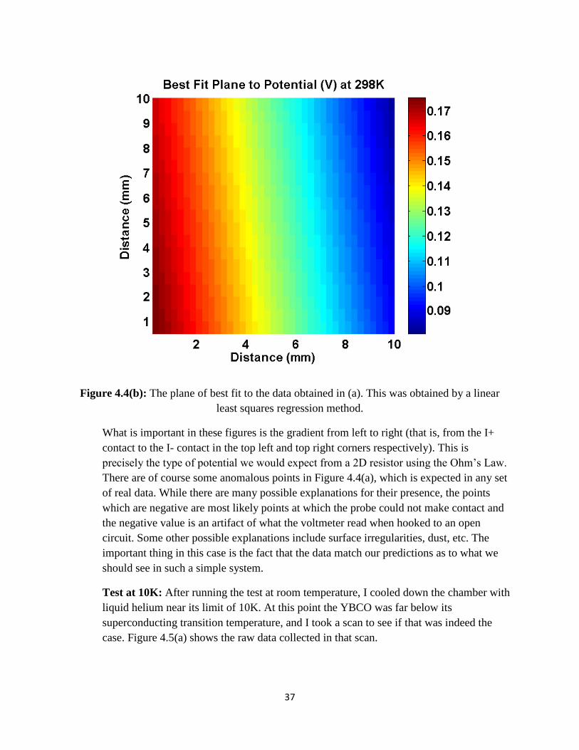
Figure 4.4(b): The plane of best fit to the data obtained in (a). This was obtained by a linear
least squares regression method.
What is important in these figures is the gradient from left to right (that is, from the I+
contact to the I- contact in the top left and top right corners respectively). This is
precisely the type of potential we would expect from a 2D resistor using the Ohm’s Law.
There are of course some anomalous points in Figure 4.4(a), which is expected in any set
of real data. While there are many possible explanations for their presence, the points
which are negative are most likely points at which the probe could not make contact and
the negative value is an artifact of what the voltmeter read when hooked to an open
circuit. Some other possible explanations include surface irregularities, dust, etc. The
important thing in this case is the fact that the data match our predictions as to what we
should see in such a simple system.
Test at 10K: After running the test at room temperature, I cooled down the chamber with
liquid helium near its limit of 10K. At this point the YBCO was far below its
superconducting transition temperature, and I took a scan to see if that was indeed the
case. Figure 4.5(a) shows the raw data collected in that scan.
38
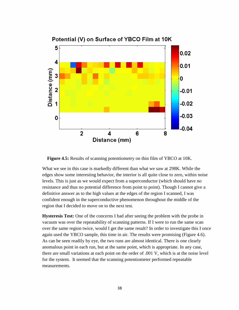
Figure 4.5: Results of scanning potentiometry on thin film of YBCO at 10K.
What we see in this case is markedly different than what we saw at 298K. While the
edges show some interesting behavior, the interior is all quite close to zero, within noise
levels. This is just as we would expect from a superconductor (which should have no
resistance and thus no potential difference from point to point). Though I cannot give a
definitive answer as to the high values at the edges of the region I scanned, I was
confident enough in the superconductive phenomenon throughout the middle of the
region that I decided to move on to the next test.
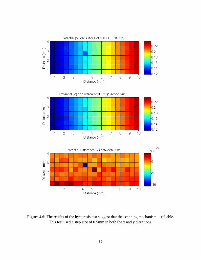
Hysteresis Test: One of the concerns I had after seeing the problem with the probe in
vacuum was over the repeatability of scanning patterns. If I were to run the same scan
over the same region twice, would I get the same result? In order to investigate this I once
again used the YBCO sample, this time in air. The results were promising (Figure 4.6).
As can be seen readily by eye, the two runs are almost identical. There is one clearly
anomalous point in each run, but at the same point, which is appropriate. In any case,
there are small variations at each point on the order of .001 V, which is at the noise level
for the system. It seemed that the scanning potentiometer performed repeatable
measurements.
39
Figure 4.6: The results of the hysteresis test suggest that the scanning mechanism is reliable.
This test used a step size of 0.5mm in both the x and y directions.
40
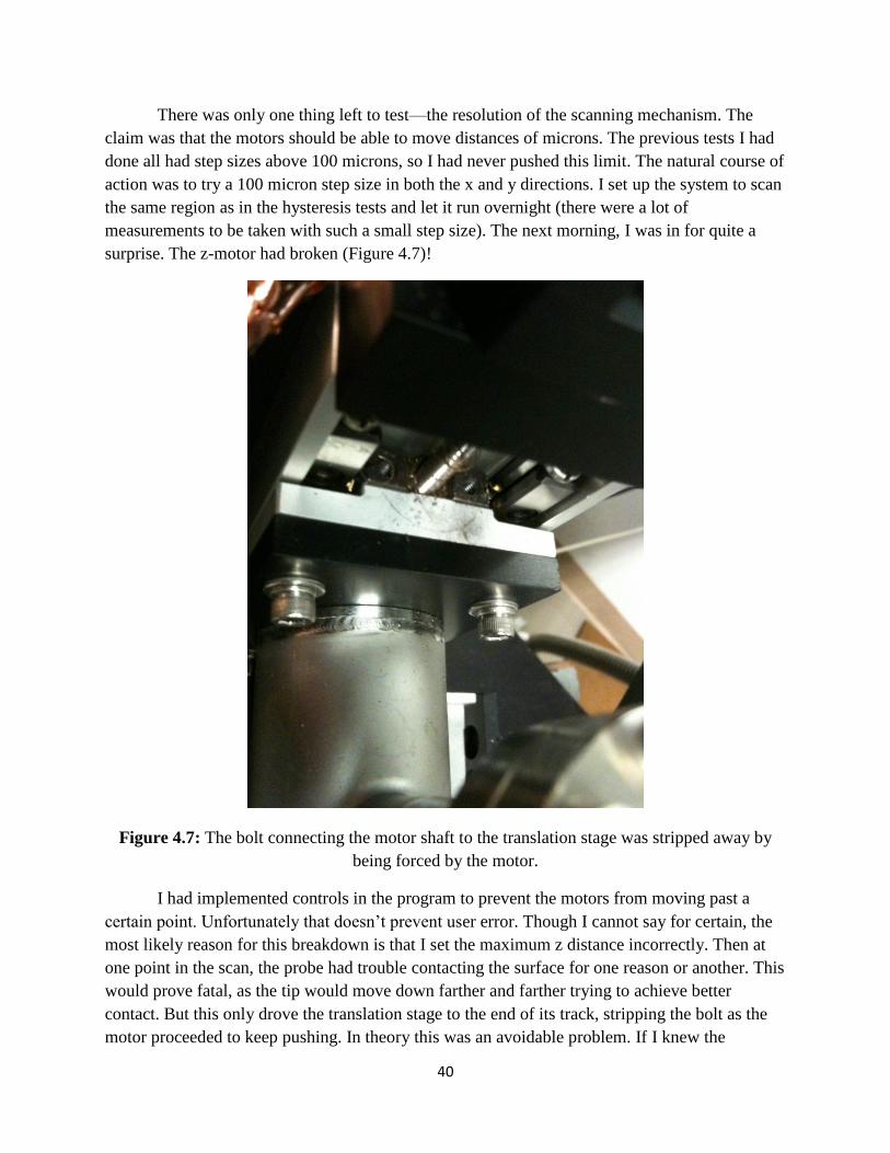
There was only one thing left to test—the resolution of the scanning mechanism. The
claim was that the motors should be able to move distances of microns. The previous tests I had
done all had step sizes above 100 microns, so I had never pushed this limit. The natural course of
action was to try a 100 micron step size in both the x and y directions. I set up the system to scan
the same region as in the hysteresis tests and let it run overnight (there were a lot of
measurements to be taken with such a small step size). The next morning, I was in for quite a
surprise. The z-motor had broken (Figure 4.7)!
Figure 4.7: The bolt connecting the motor shaft to the translation stage was stripped away by
being forced by the motor.
I had implemented controls in the program to prevent the motors from moving past a
certain point. Unfortunately that doesn’t prevent user error. Though I cannot say for certain, the
most likely reason for this breakdown is that I set the maximum z distance incorrectly. Then at
one point in the scan, the probe had trouble contacting the surface for one reason or another. This
would prove fatal, as the tip would move down farther and farther trying to achieve better
contact. But this only drove the translation stage to the end of its track, stripping the bolt as the
motor proceeded to keep pushing. In theory this was an avoidable problem. If I knew the
41
absolute position of the stage at all times I could have easily stopped this from happening. But
without some sort of external sensor, the only positioning information about the probe is relative
to its starting position. Hence operator error, for the time being, is still a danger.
Nevertheless, the broken motor, while inconvenient, was fixable. After some time spent
rewiring, the motors were fully functional yet again. However, time was running short, and I had
to start working on the real sample—Bismuth Selenide ( ).
The Perils of
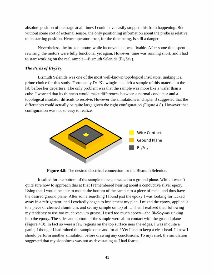
Bismuth Selenide was one of the most well-known topological insulators, making it a
prime choice for this study. Fortunately Dr. Kidwingira had left a sample of this material in the
lab before her departure. The only problem was that the sample was more like a wafer than a
cube. I worried that its thinness would make differences between a normal conductor and a
topological insulator difficult to resolve. However the simulations in chapter 3 suggested that the
differences could actually be quite large given the right configuration (Figure 4.8). However that
configuration was not so easy to realize.
Figure 4.8: The desired electrical connection for the Bismuth Selenide.
It called for the bottom of the sample to be connected to a ground plane. While I wasn’t
quite sure how to approach this at first I remembered hearing about a conductive silver epoxy.
Using that I would be able to mount the bottom of the sample to a piece of metal and thus have
the desired ground plane. After some searching I found just the epoxy I was looking for tucked
away in a refrigerator, and I excitedly began to implement my plan. I mixed the epoxy, applied it
to a piece of cleaned aluminum, and set my sample on top of it. Then I realized that, following
my tendency to use too much vacuum grease, I used too much epoxy—the was sinking
into the epoxy. The sides and bottom of the sample were all in contact with the ground plane
(Figure 4.9). In fact so were a few regions on the top surface near the edges. I was in quite a
panic; I thought I had ruined the sample once and for all! Yet I had to keep a clear head. I knew I
should perform another simulation before drawing any conclusions. To my relief, the simulation
suggested that my sloppiness was not as devastating as I had feared.

42
Figure 4.9: mounted on aluminum plate with low-temperature conductive silver epoxy.
Note that the epoxy is contacting the sides of the sample and the edges of the top.
There was then only one thing left to do—wire bond (Figure 4.10). Once again, all my
attempts to wire bond to the sample were futile. I could not even succeed at bonding to the
contact pads on the chip. Not even Katherine’s skill could save me this time, as even she
couldn’t bond to the surface of the . The sample needed something extra to help the bonds
stick. With Katherine’s help, I tried depositing gold on the surface of the sample using the so-
called RIBE machine, a homemade deposition machine whose name now bears no relation to its
function. After a few tries, the gold stuck on the surface, and we tried wire bonding again. This
time, miraculously, one bond stuck! Unfortunately that’s all that we could get, which doesn’t
quite make for a 4-point measurement. But given the time constraints it would be better to test it
like that than not test it at all. I placed the sample in the chamber and hooked it up, only to
realize that the wires inside the chamber had, once again, broken. I scurried to replace the wires,
making a new set of pins for contact, which required a fair amount of time as I had to let some
epoxy set. Once I had finally finished with the new wires, I hooked them up inside the chamber,
only to realize that the one wire bond had come off.
Figure 4.10: mounted on aluminum plate waiting to be wire bonded.
43
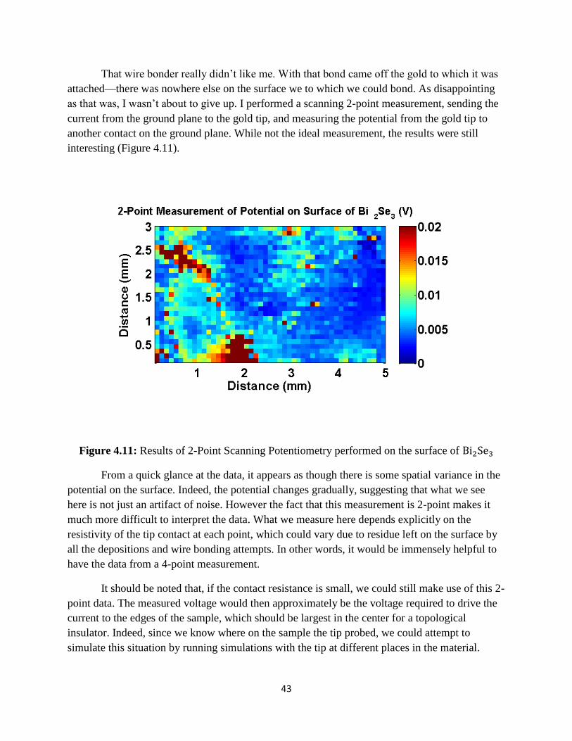
That wire bonder really didn’t like me. With that bond came off the gold to which it was
attached—there was nowhere else on the surface we to which we could bond. As disappointing
as that was, I wasn’t about to give up. I performed a scanning 2-point measurement, sending the
current from the ground plane to the gold tip, and measuring the potential from the gold tip to
another contact on the ground plane. While not the ideal measurement, the results were still
interesting (Figure 4.11).
Figure 4.11: Results of 2-Point Scanning Potentiometry performed on the surface of
From a quick glance at the data, it appears as though there is some spatial variance in the
potential on the surface. Indeed, the potential changes gradually, suggesting that what we see
here is not just an artifact of noise. However the fact that this measurement is 2-point makes it
much more difficult to interpret the data. What we measure here depends explicitly on the
resistivity of the tip contact at each point, which could vary due to residue left on the surface by
all the depositions and wire bonding attempts. In other words, it would be immensely helpful to
have the data from a 4-point measurement.
It should be noted that, if the contact resistance is small, we could still make use of this 2-
point data. The measured voltage would then approximately be the voltage required to drive the
current to the edges of the sample, which should be largest in the center for a topological
insulator. Indeed, since we know where on the sample the tip probed, we could attempt to
simulate this situation by running simulations with the tip at different places in the material.
44
Given the large number of data points taken, this would not be a trivial amount of simulations to
perform, and at this point I have not undertaken such a task.
However, it would be best, at this point, to start with a new sample. A more delicate
preparation (and perhaps another method of making contact besides wire bonding) would make
for a much cleaner experiment. Furthermore, I noticed after performing the above measurement
that the probe made small indentation marks on the surface of the sample. I had neglected to
think about the hardness of . Thus the sample surface is no longer smooth. On the bright
side, the pattern left by the scanning motion was quite regular, meaning that the scanning system
was working just as planned. In the future, of course, it is likely that a slower approach is
necessary to prevent such indentations from occurring. While this could slow down the process
considerably, it must be done to prevent pitting of the surface. This may not be a problem for all
materials of course, so one could perform a quick test beforehand to determine whether or not
more care needs to be taken.
45
Conclusion:
I couldn’t call this experiment a complete success, but it would be outright wrong to call
it a total failure. Nonetheless, I was not able to accomplish everything I had wished. Though I
tried to measure the potential on the surface of a topological insulator, the realities of lab work
foiled my attempts. But perseverance is the key in this case. The experimental apparatus itself
worked, the program worked, the simulations worked—the only thing that I couldn’t fix in time
was the sample. For that reason then, I am not downtrodden that I was not able to characterize or
much less identify a topological insulator. Indeed I haven’t shown that it is impossible! And
though my time here may have ran out, I hope the legacy that I left, in the form of this work here,
will provide a starting point for another.

46
References:
[1] L. Fu and C. L. Kane, Phys. Rev. B 76, 045302 (2007).


![A Stable-Isotope Mass Spectrometry-Based Metabolic ... · community [15]. Identifying and characterizing the phytoplankton “footprint” from the complex background of dissolved](https://img.pdfslide.us/doc/110x75/5ed95607f59b0f56f45f4c7d/a-stable-isotope-mass-spectrometry-based-metabolic-community-15-identifying.jpg)
![arXiv:1503.07493v1 [nlin.CD] 25 Mar 2015 · assure full topological conjugacy, the results of nonlinear time-series analysis can be helpful in understanding, characterizing, and predicting](https://img.pdfslide.us/doc/110x75/5edc3011ad6a402d6666bf43/arxiv150307493v1-nlincd-25-mar-2015-assure-full-topological-conjugacy-the.jpg)