Embed Size (px)
Citation preview

Simpact, Inc.9210 Sky Park CourtSan Diego, CA 92123
ICP2432Hardware Description and
Theory of Operation
DC 900-1501A
February 1998

Simpact, Inc.9210 Sky Park CourtSan Diego, CA 92123(619) 565-1865
ICP2432 Hardware Description and Theory of Operation© 1998 Simpact, Inc. All rights reservedPrinted in the United States of America
This document can change without notice. Simpact, Inc. accepts no liability for any errors this document might contain.
PLD is a trademark of Monolithic Memories Incorporated.SingleStep is a trademark of Software Development Systems, Incorporated.Z-BUS and IUSC are trademarks of Zilog Corporation.

DC 900-1501A
3
Contents
Preface 11
1 ICP2432 Overview 15
1.1 Purpose of the ICP2432 . . . . . . . . . . . . . . . . . . . . . . . . . . . 15
1.2 ICP2432 Applications . . . . . . . . . . . . . . . . . . . . . . . . . . . . 17
2 System Operations 19
2.1 ICP2432 Architecture Overview . . . . . . . . . . . . . . . . . . . . . . 19
2.2 General Operation. . . . . . . . . . . . . . . . . . . . . . . . . . . . . . 21
2.2.1 Startup . . . . . . . . . . . . . . . . . . . . . . . . . . . . . . . . . 21
2.2.2 Routine Operation . . . . . . . . . . . . . . . . . . . . . . . . . . . 21
2.2.3 Reset. . . . . . . . . . . . . . . . . . . . . . . . . . . . . . . . . . . 21
2.3 Operation in the Application Environment . . . . . . . . . . . . . . . . 22
2.3.1 Communications Traffic . . . . . . . . . . . . . . . . . . . . . . . . 22
2.3.2 Ports. . . . . . . . . . . . . . . . . . . . . . . . . . . . . . . . . . . 22
3 Hardware Survey 23
3.1 Architecture . . . . . . . . . . . . . . . . . . . . . . . . . . . . . . . . . 23
3.1.1 Dual-bus Architecture . . . . . . . . . . . . . . . . . . . . . . . . . 23
3.1.2 PCI Interface . . . . . . . . . . . . . . . . . . . . . . . . . . . . . . 25
3.2 Memory Map . . . . . . . . . . . . . . . . . . . . . . . . . . . . . . . . 25
3.2.1 Non-volatile Memory . . . . . . . . . . . . . . . . . . . . . . . . . 25
3.2.2 Peripheral Space . . . . . . . . . . . . . . . . . . . . . . . . . . . . 25
3.2.3 Volatile Memory . . . . . . . . . . . . . . . . . . . . . . . . . . . . 28
3.2.4 Z-BUS Space . . . . . . . . . . . . . . . . . . . . . . . . . . . . . . 28
3.2.4.1 Reserved Space . . . . . . . . . . . . . . . . . . . . . . . . . . 28
3.2.4.2 Peripheral Devices . . . . . . . . . . . . . . . . . . . . . . . . 28

4
DC 900-1501A
ICP2432 Hardware Description and Theory of Operation
3.3 Processor Bus. . . . . . . . . . . . . . . . . . . . . . . . . . . . . . . . . 30
3.3.1 68349 Integrated Processor . . . . . . . . . . . . . . . . . . . . . . . 30
3.3.1.1 CPU030 Processor . . . . . . . . . . . . . . . . . . . . . . . . 30
3.3.1.2 On-chip Peripherals . . . . . . . . . . . . . . . . . . . . . . . 32
3.3.1.3 68349 Power-up Defaults. . . . . . . . . . . . . . . . . . . . . 34
3.3.1.4 System Configuration and Protection . . . . . . . . . . . . . . 35
3.3.2 Chip Select Registers . . . . . . . . . . . . . . . . . . . . . . . . . . 36
3.3.3 Volatile Memory (DRAM) . . . . . . . . . . . . . . . . . . . . . . . 36
3.3.4 Non-volatile Memory (FLASH) . . . . . . . . . . . . . . . . . . . . 37
3.3.4.1 Diagnostics . . . . . . . . . . . . . . . . . . . . . . . . . . . . 37
3.3.4.2 Downloader . . . . . . . . . . . . . . . . . . . . . . . . . . . . 38
3.3.5 Debug Port . . . . . . . . . . . . . . . . . . . . . . . . . . . . . . . 38
3.4 Communications Bus (Z-BUS) . . . . . . . . . . . . . . . . . . . . . . . 40
3.4.1 Communication Devices with Integral DMA . . . . . . . . . . . . . 40
3.4.1.1 ICP2432 IUSC Configuration . . . . . . . . . . . . . . . . . . 41
3.4.2 Circuits . . . . . . . . . . . . . . . . . . . . . . . . . . . . . . . . . 42
3.4.3 Clock Steering . . . . . . . . . . . . . . . . . . . . . . . . . . . . . . 43
3.4.4 Test Mode Input Register . . . . . . . . . . . . . . . . . . . . . . . . 43
3.4.5 Sipex Mode Select Register . . . . . . . . . . . . . . . . . . . . . . . 44
3.4.6 Board ID Register . . . . . . . . . . . . . . . . . . . . . . . . . . . . 44
3.5 PCI Interface . . . . . . . . . . . . . . . . . . . . . . . . . . . . . . . . . 45
3.5.1 PCI Configuration Registers . . . . . . . . . . . . . . . . . . . . . . 45
3.6 Details of Operation . . . . . . . . . . . . . . . . . . . . . . . . . . . . . 48
3.6.1 Interrupts . . . . . . . . . . . . . . . . . . . . . . . . . . . . . . . . 48
3.6.1.1 Interrupt Operation . . . . . . . . . . . . . . . . . . . . . . . 48
3.6.1.2 Interrupt Level Assignments . . . . . . . . . . . . . . . . . . . 48
3.6.2 Timing . . . . . . . . . . . . . . . . . . . . . . . . . . . . . . . . . . 49
3.6.2.1 Clock Generation . . . . . . . . . . . . . . . . . . . . . . . . 49
3.6.2.2 Transaction Timing. . . . . . . . . . . . . . . . . . . . . . . . 50
3.6.3 Z-BUS Operation . . . . . . . . . . . . . . . . . . . . . . . . . . . . 51
3.6.3.1 Bus Conversion State Machine . . . . . . . . . . . . . . . . . . 51
3.6.3.2 Interrupt and DMA Arbitration . . . . . . . . . . . . . . . . . 51
3.6.4 Reset . . . . . . . . . . . . . . . . . . . . . . . . . . . . . . . . . . . 54
3.6.5 Non-maskable Interrupt (NMI) . . . . . . . . . . . . . . . . . . . . 55
3.7 I/O Port Details . . . . . . . . . . . . . . . . . . . . . . . . . . . . . . . 55
3.7.1 Two-port Baseboard . . . . . . . . . . . . . . . . . . . . . . . . . . 55

Contents
DC 900-1501A
5
3.7.2 Four-port Mezzanine Board . . . . . . . . . . . . . . . . . . . . . . 55
3.7.3 Eight-port Mezzanine Board. . . . . . . . . . . . . . . . . . . . . . 58
Index 59

6
DC 900-1501A
ICP2432 Hardware Description and Theory of Operation

DC 900-1501A
7
List of Figures
Figure 1–1: ISO OSI Reference Model . . . . . . . . . . . . . . . . . . . . . . . . . . 17
Figure 2–1: ICP2432 Architecture Overview . . . . . . . . . . . . . . . . . . . . . . . 20
Figure 3–1: ICP2432 Block Diagram . . . . . . . . . . . . . . . . . . . . . . . . . . . 24
Figure 3–2: ICP2432 Memory Map. . . . . . . . . . . . . . . . . . . . . . . . . . . . 26
Figure 3–3: Detailed Processor Bus Memory Map . . . . . . . . . . . . . . . . . . . . 27
Figure 3–4: Detailed Z-BUS Memory Map. . . . . . . . . . . . . . . . . . . . . . . . 29
Figure 3–5: 68349 Integrated Processor Block Diagram. . . . . . . . . . . . . . . . . 31
Figure 3–6: Test Mode Register . . . . . . . . . . . . . . . . . . . . . . . . . . . . . . 43
Figure 3–7: PCI Interface Block Diagram . . . . . . . . . . . . . . . . . . . . . . . . 46
Figure 3–8: PCI Configuration Space Header . . . . . . . . . . . . . . . . . . . . . . 47
Figure 3–9: ICP2432 System Timing . . . . . . . . . . . . . . . . . . . . . . . . . . . 50
Figure 3–10: Z-BUS Arbitration Block Diagram . . . . . . . . . . . . . . . . . . . . . 52
Figure 3–11: Interrupt and DMA Priority Arbitration . . . . . . . . . . . . . . . . . . 53
Figure 3–12: Signal Mapping for the 37-pin EIA-449 Interface . . . . . . . . . . . . . 56
Figure 3–13: Signal Mapping for the 25-pin EIA-530 Interface . . . . . . . . . . . . . 57
Figure 3–14: Signal Mapping for the 25-pin EIA-232 Interface . . . . . . . . . . . . . 57

8
DC 900-1501A
ICP2432 Hardware Description and Theory of Operation

DC 900-1501A
9
List of Tables
Table 1–1: ICP Hardware Features and Benefits . . . . . . . . . . . . . . . . . . . . . 16
Table 3–1: Device Parameters . . . . . . . . . . . . . . . . . . . . . . . . . . . . . . 36
Table 3–2: Debug Module to ICP . . . . . . . . . . . . . . . . . . . . . . . . . . . . 39
Table 3–3: Debug Module to Terminal. . . . . . . . . . . . . . . . . . . . . . . . . . 39
Table 3–4: Interface Circuits . . . . . . . . . . . . . . . . . . . . . . . . . . . . . . . 42
Table 3–5: Transaction Timing . . . . . . . . . . . . . . . . . . . . . . . . . . . . . . 50

10
DC 900-1501A
ICP2432 Hardware Description and Theory of Operation

DC 900-1501A
11
Preface
Purpose of Document
This manual describes Simpact’s ICP2432 front-end communications processor, its
architecture, and how it works in an PCIbus system.
Intended Audience
This document should be read by maintenance technicians, computer system integra-
tors, and software developers who need detailed information about the operating the-
ory and features of the ICP2432 hardware.
Required Equipment
The ICP2432 board mounts in any full PCIbus slot that supports bus mastering.
Organization of Document
If you are not familiar with Simpact’s front-end communications processors, you
should read Chapter 1 and Chapter 2. If you are familiar with front-end communica-
tions processors, you may wish to skip these overviews and go directly to the detailed
technical descriptions in Chapter 3.
Chapter 1 contains a functional overview of the ICP2432.
Chapter 2 describes the basic operation of the ICP2432 in a system.
Chapter 3 contains a detailed theory of operation with hardware descriptions.

12
DC 900-1501A
ICP2432 Hardware Description and Theory of Operation
References
Central Processor Unit Reference Manual
, CPU32+RM/AD, Motorola, Inc.
ICP2432-to-PCI Host Protocol Specification
, Simpact, Inc., DC-900-1509
MC68349 Integrated Processor with DMA User’s Manual
, MC68349UM/AD,
Motorola Inc.
S5933 PCI Controller Data Book
, AMCC
Z16C30/Z16C32 IUSC User’s Manual
, Zilog, Inc.
Document Conventions
The following conventions apply throughout this document:
•
A signal name that appears with an overline, for example, ZAS, indicates that the
signal is asserted low true.
•
“Communications bus” is equivalent to “Z-BUS.”
•
Bits are numbered from right to left, beginning with zero. Bit zero is the low-order
bit.
•
Hexadecimal values are shown with the notation (hex). The underscore (_) is for
readability purposes only.

Preface
DC 900-1501A
13
Revision History
The revision history of the
ICP2432 Hardware Description and Theory of Operation
,
Simpact document DC900-1501, is recorded below:
Customer Support
If you are having trouble with any Simpact product, call us at 1-800-275-3889 Monday
through Friday between 8 a.m. and 5 p.m. Pacific time.
You can also fax your questions to us at (619)560-2838 or (619)560-2837 any time.
Please include a cover sheet addressed to “Customer Service.”
We are always interested in suggestions for improving our products. You can use the
report form in the back of this manual to send us your recommendations.
Document Revision Release Date Description
DC 900-1501A February 1998 Original release

14
DC 900-1501A
ICP2432 Hardware Description and Theory of Operation

DC 900-1501A
15
Chapter
1
ICP2432 Overview
The ICP2432 intelligent communications processor is an ancillary computer dedicated
to the processing of communications-related data.
The ICP2432 hardware is a single-board computer with a central processing unit
(CPU), random access memory (RAM), programmable read-only memory (PROM),
and input/output (I/O) circuitry. The software consists of an onboard operating sys-
tem, diagnostic tests, host interface drivers, and application routines.
1.1 Purpose of the ICP2432
The main purpose of the ICP2432 is to improve the overall computing efficiency of the
host computer. To do this, low-level communications tasks traditionally performed by
the host central processor are migrated to the ICP.
An ICP increases overall system bandwidth by distributing the I/O processing away
from the host CPU. In the traditional minicomputer or microcomputer architecture,
the host services all I/O requests. This load on the CPU has grown steadily as computer
peripherals have become increasingly more powerful. Modern operating systems allow
intelligent front-end processors to perform these relatively simple tasks. The result is an
overall increase in system throughput.
Table 1–1 sums up the attributes of the ICP.

16
DC 900-1501A
ICP2432 Hardware Description and Theory of Operation
Table 1–1:
ICP Hardware Features and Benefits
Features Benefits
68349 integrated processor4-gigabyte linear address space Allows use of familiar, powerful program development tools (assemblers, C compiler, editors)Integrated DMA support for PCI transfers
S5933 PCI interface 32-bit master/slave interfacePCI revision 2.1 compliant
Large RAM memorySpace for application tasks and real-time executiveApplications are downloaded from the host rather than from ROM to make it easier to update software
Individually programmable ports
One ICP services lines with different characteristicssuch as parity, data rate, synchronous
vs.
asynchronous, CRC checkingFull modem supportFlexibility in changing environments
DMA-controlled data transfer Full duplex support for high-speed applications
Multiple electrical interfacesSupports EIA-232 (V.28), EIA-422 (V.11 and X.27), EIA-423 (V.10 and X.26), EIA-449, EIA-485, EIA-530, EIA-562, MIL-STD-188C, MIL-STD-188-114A Unbal-anced, MIL-STD-188-114A Balanced Type II, and V.35
Single-module form factor Easy mounting in standard backplane

1: ICP2432 Overview
DC 900-1501A
17
1.2 ICP2432 Applications
The ICP2432 is a general-purpose computer that can do many different tasks. At system
startup, the ICP2432 gains its run-time personality from downloaded application soft-
ware. The application software may be customer-specific or part of an ICP2432 turnkey
product.
Communications software systems that use the ICP2432 can fit the International Stan-
dards Organization (ISO) open system interconnection (OSI) seven-layer reference
model for communications protocols. Figure 1–1 shows this model. In most cases the
ICP is programmed to perform up to the first three levels of this model.
Once the software download has been completed, the ICP2432 hardware and software
combination performs its assigned task until a board-level reset initiates another
startup sequence.
Figure 1–1:
ISO OSI Reference Model
APPLICATION
PRESENTATION
SESSION
TRANSPORT
NETWORK
DATA LINK
PHYSICAL
7
6
5
4
3
2
1
LayerNumber Function
Services applications
Code conversion, data format
Coordinates interaction between applications
End-to-end data integrity
Routes information
Exchanges data with physical link
Transmits/receives bit stream to medium
3042

18
DC 900-1501A
ICP2432 Hardware Description and Theory of Operation

DC 900-1501A
19
Chapter
2
System Operations
This chapter describes the ICP2432 hardware and its operation in host systems.
2.1 ICP2432 Architecture Overview
The ICP2432 computer provides high-performance, front-end processing in commu-
nications environments as shown in Figure 2–1. The processor bus consists of a CPU,
memory, and PCI interface and support devices. This bus is used to execute the appli-
cation program and provide computing resources as required by high-level protocols.
The communications bus (the subsidiary bus) consists of the communications devices
with integral DMA controllers. This bus is used for the movement of data between the
serial ports and memory buffers. These two independent buses are bridged by circuitry
that translates appropriate signals to control transactions between them during inter-
bus operations.

20
DC 900-1501A
ICP2432 Hardware Description and Theory of Operation
Figure 2–1:
ICP2432 Architecture Overview
Pro
cess
or B
us
AAAAAAAA
Host PCIbus
PCIInterface
Memory
ICP2432
CPU
Communications I/O
Communications Channels
Com
mu
nic
atio
ns
Bu
s
3287
EPROM
Inter-bus Control
MezzanineConnector

2: System Operations
DC 900-1501A
21
2.2 General Operation
Operation of the ICP2432 occurs in two phases: startup and routine operation. When
power is initially applied to the ICP2432, its CPU begins execution at a memory address
in the PROM device. This location contains instructions to set up the basic working
environment for the CPU.
2.2.1 Startup
Startup begins with the execution of diagnostic firmware that tests the major sections of
the ICP2432 hardware. Upon successful completion of these tests, the PCI interface is
initialized and the host downloads the ICP’s operating system and application program
software, through the PCIbus interface circuits, into the ICP memory. After these pro-
grams have been downloaded, the CPU begins to execute the downloaded software.
2.2.2 Routine Operation
During routine operation, the ICP2432 does all the communications-related work. The
software program downloaded during startup is used to operate the general-purpose
ICP2432 communications hardware in the mode required by the host system. This pro-
gram is typically an implementation of some special purpose communications protocol
such as X.25, SDLC, or ADCCP.
The ICP2432 remains in the routine phase of operation until a board reset is issued by
the host software, the host-bus hardware, or the reset button.
2.2.3 Reset
A hardware reset causes the ICP2432 to stop execution of program instructions. No
attempt is made to save the current state of the CPU operation. The hardware reset
causes the CPU to go back to the startup phase.

22
DC 900-1501A
ICP2432 Hardware Description and Theory of Operation
2.3 Operation in the Application Environment
The ICP2432 offloads the host, thus increasing overall system performance. Tradition-
ally, the host’s CPU executes the tasks related to the operation of serial communica-
tions. These tasks can be extensive, and many require processing in real time. The
ICP2432 hardware, combined with application software, is capable of executing many
of these protocol-dependent, low-level tasks. The ICP2432 receives the application soft-
ware download from the host system during the system startup phase.
2.3.1 Communications Traffic
When the software download is complete, communications traffic is accepted and pro-
cessed for transfer to or from the host. In most applications, the data format used by the
host processor is very different from the format transmitted on the serial communica-
tions links. Many additional structures must be added to the raw data processed by the
host system in order to detect errors, retransmit frames, and maintain data integrity at
the data link level. The software programs downloaded into the ICP2432 perform these
tasks.
2.3.2 Ports
The ICP2432 is equipped with two, four, or eight high-performance serial communica-
tions ports. The ICP2432, when combined with the appropriate distribution cables
and/or adapters, can support such electrical interface specifications as EIA-232 (V.28),
EIA-422 (V.11 and X.27), EIA-423 (V.10 and X.26), EIA-449, EIA-485, EIA-530, EIA-
562, MIL-STD-188C, MIL-STD-188-114A Unbalanced, MIL-STD-188-114A Balanced
Type II, and V.35.

DC 900-1501A
23
Chapter
3
Hardware Survey
This chapter describes the ICP2432 architecture, memory map, buses, and devices.
Refer to the block diagram of the board, Figure 3–1, throughout the chapter.
3.1 Architecture
The ICP2432 is a single-board computer designed to optimize communications pro-
cessing for systems with PCIbus support. The base configuration has two high-speed
serial ports. Four- and eight-port mezzanine configurations are optional. Devices are
not installed in the on-board port locations when a mezzanine board is used. See
Figure 3–1.
3.1.1 Dual-bus Architecture
The ICP2432 uses a dual-bus architecture to overcome the limitations that high-speed
data lines impose on CPU processing power. The processing engine resides on a proces-
sor bus while the serial communications devices with their integral DMA controllers
reside on an isolated Z-BUS. Each of these buses is optimized for its primary function.
The processor bus has a Motorola MC68349 32-bit processor, longword-wide memory,
and a non-multiplexed bus architecture that is optimized for program execution. The
communications bus is implemented as a Zilog 16-bit multiplexed bus (Z-BUS) that is
optimized for DMA-controlled serial data movement. The 68349 CPU has access to the
memory and all devices on both buses, whereas the DMA devices on the Z-BUS have
access only to the memory system.

24
DC 900-1501A
ICP2432 Hardware Description and Theory of Operation
Figure 3–1:
ICP2432 Block Diagram
3046
AMCCS5933
32-bit PCIbus
8 MBDRAM Memory
(2MB x 32)
FLASH32K x 8
32-bit Processor Bus
2 ports “on-board” removedif using mezzanine option
Z-BUS conversion, arbitration, isolation, and mezzanine connector
Z-BUS
Z16C32IUSC
SP503 software-configurable electrical
interface
26-pinI/O
ConnectorElectrical Interface
Devices
100-pinI/O
Connector
Mezzanine Board Options:4-port multi EIG (full modem)8-port EIA-232 (full modem)
26-pinI/O
Connector
SP504 Software-Configurable
Electrical Interface
Z16C32IUSC
MC68349Integrated
CPU
DMA

3: Hardware Survey
DC 900-1501A
25
3.1.2 PCI Interface
In most cases, the host machine is the ultimate source or destination of the data being
transmitted and received through the serial communications devices. The board
requires a mechanism for issuing commands, determining status, and controlling data
exchange with the host system in which it resides.
The ICP2432 provides both a 32-bit PCIbus master and bus slave “end point” device
(not a bridge). It is a 33 Mhz, +5v interface compliant with Rev 2.1 of the
PCI Local Bus
Specification
. See Section 3.5 on page 45 for details.
3.2 Memory Map
The ICP2432 memory map, shown in Figure 3–2, is divided into four main sections:
non-volatile memory space, peripheral space, volatile memory space, and Z-BUS space.
These main sections are expanded further as illustrated in Figure 3–3 and Figure 3–4 to
show detailed addressing information.
3.2.1 Non-volatile Memory
The four-megabyte space beginning at address 000_0000 hex is the non-volatile mem-
ory space. See Figure 3–3 on page 27. The ICP2432 FLASH occupies the lowest
64 kilobytes. The additional space is reserved for future expansion.
3.2.2 Peripheral Space
The four-megabyte space beginning at address 040_0000 hex is the peripheral device
space. See Figure 3–3 on page 27. To simplify the address decoding logic on the board,
each peripheral device is assigned a 64 kilobyte window. The ICP2432 has one assigned
device: the PCI interface device (see Section 3.5 on page 45). The additional space is
reserved for future expansion.

26
DC 900-1501A
ICP2432 Hardware Description and Theory of Operation
Figure 3–2:
ICP2432 Memory Map
4 Mbytes
4 Mbytes
8 Mbytes
16 Mbytes
3047
03F_FFFF
Non-volatileMemory
Space
000_0000
07F_FFFF
Peripheral Space
040_0000
0FF_FFFF
VolatileMemory
Space
080_0000
1FF_FFFF
Z-BUS Space
100_0000

3: Hardware Survey
DC 900-1501A
27
Figure 3–3:
Detailed Processor Bus Memory Map
3291
03F_FFFF
Non-volatileMemory
Space
000_0000
07F_FFFF
Peripheral Space
040_0000
0FF_FFFF
VolatileMemory
Space
080_0000
1FF_FFFF
Z-BUS Space
100_0000
8 MbyteDRAM Bank 0
043_0000
Reserved forExpansion
PCI Interface042_0000
041_0000
040_0000 Reserved
64 kbytesFLASH
000_0000
000_FFFF
Reserved forExpansion
001_0000
03F_FFFF
Reserved
0FF_FFFF
080_0000
07F_FFFF

28
DC 900-1501A
ICP2432 Hardware Description and Theory of Operation
3.2.3 Volatile Memory
The eight-megabyte space beginning at address 080_0000 hex is the volatile memory
space. See Figure 3–3 on page 27. ICP-standard DRAM occupies the entire eight mega-
bytes of this space.
3.2.4 Z-BUS Space
The 16-megabyte space beginning at address 100_0000 hex is the Z-BUS space. See
Figure 3–4 on page 29. This is further divided into specific address sections: a section
reserved for memory expansion and the peripheral device section.
3.2.4.1 Reserved Space
The eight-megabyte space beginning at 100_0000 hex is reserved for memory expan-
sion on future mezzanine board products.
3.2.4.2 Peripheral Devices
The eight-megabyte space beginning at 180_0000 hex is used for Z-BUS peripheral
devices. To simplify address decoding logic, each device is assigned a four-kilobyte win-
dow. These devices are the integrated universal serial controllers (IUSCs) with integral
DMA controllers (Section 3.4.1 on page 40), the EIA mode control registers for the
Sipex electrical interface devices (Section 3.4.5 on page 44), the input register for the
Test Mode inputs (Section 3.4.4 on page 43), and the board ID register (Section 3.4.6
on page 44). The additional space is reserved for future mezzanine board products.

3: Hardware Survey
DC 900-1501A
29
Figure 3–4:
Detailed Z-BUS Memory Map
100_0000
Reserved for Expansion
Z-BUS Peripheral
Devices
17F_FFFF
1FF_FFFF
180_0000
03F_FFFF
Non-volatileMemory
Space
000_0000
07F_FFFF
Peripheral Space
040_0000
0FF_FFFF
VolatileMemory
Space
080_0000
1FF_FFFF
Z-BUS Space
100_0000
3292
180_4000 IUSC4
180_6000 IUSC6
180_5000 IUSC5
180_3000 IUSC3
180_2000 IUSC2
180_1000 IUSC1
180_0000 IUSC0
180_8000 EIA _0
1FF_FFFF
181_2000
Reserved
180_7000 IUSC7
180_9000 EIA _1
180_A000 EIA _2
180_B000 EIA _3
180_C000 EIA _4
180_D000 EIA _5
180_E000 EIA _6
180_F000 EIA _7
181_0000 TMREG
181_1001 BD_ID

30
DC 900-1501A
ICP2432 Hardware Description and Theory of Operation
3.3 Processor Bus
The ICP2432 processor bus is composed of the CPU, DRAM, FLASH, PCI interface
device, and support circuitry required for timing and control of the bus. Descriptions
of the major devices, support circuitry, bus signals, and operation of the processor bus
are contained in this section. For clarity, the processor description precedes the descrip-
tions of the bus operation and other devices that connect to this bus.
3.3.1 68349 Integrated Processor
The 68349 processor, shown in Figure 3–5, is a highly integrated device that provides
extremely flexible configurations. For complete information on the 68349, see Motor-
ola’s MC68349 Integrated Processor with DMA User’s Manual. The 68349 processor
includes the following major functional blocks:
• CPU030 processor
• DMA controller
• Serial controller
• System integration module (SIM)
3.3.1.1 CPU030 Processor
The processing power for the 68349 is provided by the CPU030 central processing unit.
The CPU030 delivers full 68030 performance through the use of its three modular ele-
ments:
• CPU32+ 32-bit processor
• Configurable instruction cache (CIC)
• Quad data memory module (QDMM)
Figure 3-5, 68349, is scaled to 70%.
3: Hardware Survey
DC 900-1501A 31
Figure 3–5: 68349 Integrated Processor Block Diagram
32-bit Inter-module Bus
CPU030 Processor
SystemIntegration Module
(SIM49)
IEEE 1149.1 Test
ClockSynthesizer
Chip Selects andWait States
SystemProtection
ExternalBus Interface
InterruptControl
Quad DataMemory Module
(QDMM)
CPU32+M68000 Family
Processor
ConfigurableInstruction Cache
(CIC)
Two-channelDMA Controller
Two-channelSerial I/O
32-bit Address Bus
32-bit Data Bus
3316

32 DC 900-1501A
ICP2432 Hardware Description and Theory of Operation
CPU32+ Processor
The CPU32+ is a 32-bit execution unit with 32-bit data paths (internal and external). It
has a two-clock basic instruction execution rate for 32-bit operation. The CPU32+ is
completely software compatible with the 68000.
Configurable Instruction Cache (CIC)
The CIC is a highly configurable memory resource designed to optimize the supply of
instructions to the CPU32+. It is closely coupled to the CPU32+, but isolated from the
inter-module bus, allowing the processor to continue instruction execution while the
IUSCs DMA controllers use the external bus.
The CIC can be configured as either a 1 kilobyte instruction cache or as 2 kilobytes of
SRAM. The CIC can be used for high-priority interrupt servicing, O/S routines, or as a
general instruction cache.
Quad Data Memory Module (QDMM)
The QDMM provides four independent blocks of 1 kilobyte SRAM. The QDMM can be
used as scratchpad memory, stack caches for independent tasks, or parameter storage.
As general SRAM, this space can contain instructions for fast access to additional inter-
rupt handlers, O/S code, or other frequently accessed code.
3.3.1.2 On-chip Peripherals
The on-chip peripherals described below are independent modules. An inter-module
bus (IMB) is used for all on-chip communications. The IMB is similar to a traditional
external bus with address, data, clock, interrupt, arbitration, and handshake signals.
The IMB ensures that communication between the modules is fully synchronized and
that arbitration and interrupts can be handled in parallel with data transfers.
3: Hardware Survey
DC 900-1501A 33
Direct Memory Access Module
The 68349 contains a high-speed 32-bit DMA controller. The DMA module consists of
two independently programmable channels. Each channel has separate request,
acknowledge, and done signals. Each channel can operate in flyby or dual address mode
and supports byte, word, and longword transfers. It supports both burst and cycle steal
external request modes. The DMA controller can be configured to release the bus back
to the CPU when a high-priority interrupt occurs. The CPU32+ and the DMA control-
ler arbitrate for the bus in parallel with executing bus cycles, typically eliminating all
bus arbitration overhead and allowing DMA and CPU bus cycles to occur back-to-back
without intervening idle clocks.
The ICP2432 uses the DMA controller to move data between the memory and the
FIFOs in the PCIbus interface controller. PCI writes (data transfers from the ICP to the
host’s main memory) use DMA channel 1 configured for external request, single
address, burst writes to the S5933 FIFO. PCI reads (data transfers from the host’s main
memory to the ICP) use DMA channel 2 configured for external request, single address,
cycle-steal reads from the S5933 FIFO.
Serial Module
The 68349 contains two highly configurable full-duplex USARTs.
The ICP2432 uses serial channel A, configured as a 9600 baud asynchronous port, as a
console to provide command and status input/output to software development and
manufacturing test personnel.
The channel A RTS and CTS pins are used by diagnostic code to determine mode of
operation. Manufacturing loopback connectors tie RTSA to CTSA to signify that full
manufacturing diagnostics are to be executed.

34 DC 900-1501A
ICP2432 Hardware Description and Theory of Operation
The channel A RxRDY and TxRDY output pins are used to drive the LED indicators on
the I/O panel. See Section 3.3.5 on page 38 for console mechanical and pinout informa-
tion.
• RxRDYA drives the green LED
• TxRDYA drives the red LED
Serial channel B is not used.
System Integration Module (SIM)
The SIM49 provides the external bus interface for both the CPU32+ and the DMA
modules. It also provides programmable circuits to perform address decoding, chip
selects, wait-state insertion, interrupt handling, clock generation, bus arbitration,
watchdog timing, discrete I/O, and power-on reset timing.
The internal registers for all the modules are contained in a single 4-kilobyte block that
is relocatable along 4-kilobyte boundaries. The ICP2432-specific register implementa-
tion is integral to the hardware design and should not be modified by user application
programs.
3.3.1.3 68349 Power-up Defaults
At power-up or reset, the 68349 registers and the external pins they control are reset to
default conditions. The functionality of these pins is configurable and, since external
devices and logic are connected to them, unique to each hardware design. A method is
required to enable the 68349’s first fetches from ROM to operate properly before these
SIM control registers are initialized.
The 68349 samples several hardware inputs on the rising edge of RESET for the design-
dependent power-up configuration.

3: Hardware Survey
DC 900-1501A 35
The ICP2432 implementation pulls:
• D29 low: selects port A pins as inputs
• D31 high and D30 low: selects byte-wide global chip select
• MODCLK low: selects external clock
3.3.1.4 System Configuration and Protection
After initial power-up, the system configuration is determined by initializing the MCR
and AVR registers. These registers control the port pin functions, the debug support,
the interrupt arbitration of on-chip modules, and the external interrupts that require
auto-vector support. The ICP2432 is configured as follows:
Module Base = EE00_FF00 hexClock Mode = External with PLL (external oscillator @ 16 Mhz)
Port A-7 = out Driven high (not used)
A-6 = out IUSC interrupt acknowledges (IACK_USC)
A-5 = out Driven high (not used)
A-4 = in Mezzanine-installed indicator (MEZZ_ON)
A-3 = out Enable bus master PCI writes (PCI_W_ENB)
A-2 = out Enable bus master PCI reads (PCI_R_ENB)
A-1 = out Enables IUSC BRs (BR_ENBL)
A-0 = out Driven high (not used)
Port B-7 = in IRQ 7 for NMI interrupt
B-6 = in IRQ 6 for IUSC interrupt
B-5 = in IRQ 5 for PCI interrupt
B-4 = out CS3, Z-BUS, external DSACK, A23 high = devices
B-3 = out Driven high (not used)
B-2 = out CS2 for PCI interface, internal 0-wait, LW DSACK
B-1 = out CS1 for DRAM memory, external DSACK
B-0 = out CS0 for ROM, internal 2-wait, byte-wide DSACK(global select at power-up)
Autovector: AV7 (NMI) and AV5 (PCI) use autovector
Periodic Interrupt Timer: OS/Impact tick timer
Software Watchdog Timer: Reserved for IUSC hang
BERR Monitor: 64 clocks (4 microseconds)

36 DC 900-1501A
ICP2432 Hardware Description and Theory of Operation
The ICP2432 IARBs are:
• F = Module configuration register (MCR for SIM)
• E = DMA controller
• B = Serial controller
3.3.2 Chip Select Registers
The four chip select registers are initialized as shown in Table 3–1.
3.3.3 Volatile Memory (DRAM)
The DRAM memory is the ICP2432’s central resource and is used for both executable
code and protocol data buffers. The memory can be accessed by the 68349’s CPU32+
and DMA controller and by the integrated DMA controller within each of the IUSCs.
The 68349 provides all of the arbitration for this central memory resource. The 68349
arbitration takes place concurrently with bus transactions to ensure high bandwidth
availability. The arbitration priority, from highest to lowest, is external bus masters
(IUSCs), internal DMA controller, and CPU32+.
The memory system is implemented as a 32-bit, zero-wait state DRAM memory system
that supports byte, word, and longword access.
The refresh mechanism for ICP2432 uses embedded refresh cycles for each CPU32+
access of the FLASH or IUSCs and during each IUSC memory transaction. CPLD logic
Table 3–1: Device Parameters
Device/Memory Space Width DTACK
Processor Memory longword external, 0 wait state
FLASH byte internal, 2 wait states
PCI Interface Device longword internal, 1 wait state
Z-BUS Space word external, 2 wait states

3: Hardware Survey
DC 900-1501A 37
includes both a 16 microsecond timer and a refresh counter. The timer forces a refresh
every 16 microseconds if no embedded refreshes have occurred. The counter incre-
ments for each embedded refresh cycle completed and decrements at each 16 microsec-
ond timer interval. Embedded refreshes from multiple accesses of FLASH, IUSC, or
IUSC transactions delay timer refreshes, thereby maximizing memory bandwidth.
3.3.4 Non-volatile Memory (FLASH)
The ICP2432 requires firmware to execute manufacturing diagnostics, power-up self
tests, and the bootload code that coordinates the download of OS/Impact and protocol
images from the host.
The ICP2432 provides a 32-pin PLCC socket for a non-volatile device. The socket sup-
ports any 512 kilobit-to-4 megabit (64 kilobyte-to-512kilobyte) EPROM/FLASH/OTP
device whose footprint meets the JEDEC standard. Since the firmware code is seldom
changed, in-circuit write cycles for FLASH or EEPROM devices are not supported. A
512 kilobit (64 kilobyte) device is standard at this time.
3.3.4.1 Diagnostics
Self-test diagnostics are executed on initial power-up. These tests validate the control
circuitry, memory, processor and Z-BUS peripheral devices, interrupt operation, and
bus error logic of the ICP2432 hardware. Test status and error reporting may be moni-
tored by connecting a terminal to the console port on the optional debug module.
The successful completion of the diagnostics allows the downloader to execute on
request from the host.
Additional diagnostics are run if:
• the DTR modem signal of the ICP2432 console port drives its DCD input signal,
or
• the DCD signal is driven by a console device’s DTR and it is “true” and the console
device responds with a “p” (for production) in response to an ENQ.

38 DC 900-1501A
ICP2432 Hardware Description and Theory of Operation
The production diagnostics include IUSC DMA tests and IUSC/Sipex digital I/O loop-
back tests. These tests are not run in real environments because the data and control sig-
nals do not respond predictably without self-port loopback connectors installed.
If the console device responds with a “d” (for debug), the PROM code calls the mem-
ory/device display routine so that a programmer can examine various memory loca-
tions and device registers that may not have been changed by the reset.
Note that most program debugging should be done with a symbolic debugger such as
SingleStep from Software Development Systems, Inc., which can be downloaded with
OS/Impact and the application software.
3.3.4.2 Downloader
The CPU uses the boot loader code and the host driver to download the OS/Impact
executive and applications from the host to the board. The ICP2432 does this by mov-
ing the executable images to the onboard memory. The CPU begins execution of the
downloaded code at the completion of the download sequence.
3.3.5 Debug Port
The ICP2432 implements all debug support circuits on a plug-in module. The debug
module is intended for use by software developers, production personnel, and toolkit
customers.
The debug panel includes the following:
• Reset push-button
• NMI push-button
• EIA-232 line driver/receiver for 68349’s serial channel A
• Cable from board to module and cable from module to terminal

3: Hardware Survey
DC 900-1501A 39
The ICP baseboard has a 10-position box-header located at the back edge of the board.
This header is easily accessible and allows debug module attachment without removing
the ICP from the PCI slot. The connector for the cable between the ICP and the module
is keyed, and requires a keyed cable. Failure to properly connect the cable between the
ICP and the module will damage the circuitry on the module. The terminal connector
is keyed, but operates correctly with either cable orientation.
The debug module connector pinouts are shown in Table 3–2 and Table 3–3.
Table 3–2: Debug Module to ICP
Pin Number Signal
1 +5v
2 GND
3 TD
4 RD
5 RTS
6 CTS
7 RESET_BUTTON
8 NMI_BUTTON
9 GND
10 +5v
Table 3–3: Debug Module to Terminal
Pin Number Signal
1, 10 TD
2, 9 RD
3, 8 DTR
4, 7 DCD
5, 6 GND

40 DC 900-1501A
ICP2432 Hardware Description and Theory of Operation
3.4 Communications Bus (Z-BUS)
The ICP2432 communications bus exists as a space in the CPU memory map and is
composed of integrated universal serial controllers (IUSCs), electrical interface control
registers, a modem Test Mode input register, a board ID register, and the support cir-
cuitry required for timing, data transfer, bus arbitration, and interrupt operations. This
section gives a full description of the major devices, support circuitry, bus signals, and
operation of the communications bus. The communications bus is implemented as a
Zilog multiplexed bus and is referred to as the Z-BUS throughout this section.
3.4.1 Communication Devices with Integral DMA
The ICP2432 uses two, four, or eight Z16C32 integrated universal serial controllers
(IUSCs) with integral DMA. Each IUSC is a single-channel, multi-protocol data-com-
munications device that functions as a serial-to-parallel and parallel-to-serial data con-
verter. It may be software configured to satisfy a wide variety of serial communications
applications. Each IUSC may be programmed to handle asynchronous formats, syn-
chronous byte-oriented protocols such as IBM bisynchronous, and synchronous bit-
oriented protocols such as HDLC and IBM SDLC. The IUSC can generate and check
CRC codes in any synchronous mode and can be programmed to check data integrity
in various modes. Each IUSC includes modem control signals, data clock generation,
vector-includes-status interrupts, and an integral DMA interface.
The transmitters and receivers of each IUSC have a 32-byte FIFO that can be loaded or
emptied by byte or by word. The ICP2432 also has a nominal baud clock source of
3.6864 megahertz, plus a socket for an optional oscillator for specific, non-standard bit
clocks.
The integral DMA controllers in the IUSCs can operate in any of four modes: Single
Buffer, Pipelined, Array, and Linked List. Command and status information can be
extracted or put into the lists of the last two modes. This feature allows automated
reception of back-to-back frames of SDLC data without loss of data or frame rejection

3: Hardware Survey
DC 900-1501A 41
even at a 10 megabit per second rate. As with the serial controller sections of the IUSCs,
the DMA controller sections can generate interrupts with Vector Includes Status which
enhances interrupt response. Up to 64 kilobytes may be sent or received in one block
out of or into multiple buffers.
3.4.1.1 ICP2432 IUSC Configuration
Like the 68349, the IUSC is highly configurable and requires hardware indicators to
determine basic operation before its configuration registers are initialized. The IUSC
determines its operational mode by sampling several pins during the first write to it.
The IUSC ignores its address pins and always initializes the bus configuration register
on this first write.
The ICP2432’s initial write to each IUSC BCR is as follows:
0007h with the ZAS and S/D pins low
This results in the following operational characteristics:
• ZAS low: multiplexed, direct address bus implementation
• S/D low: WAIT/RDY pin is acknowledge for slave and IACK cycles
• IACK mode: 00, capture INTACK at start of cycle
• BRQTP: 0, open drain bus request
• 16Bit: 1, device is word-wide bus
• IRQTP: 1, open drain interrupt request
• SRight: 1, capture slave register address on AD6-0
The IUSC’s DMA clock is 8 Mhz, the baud rate generator clock is 3.6864 Mhz. Option-
ally, a 16 Mhz clock or a unique oscillator socket can be selected as sources of serial data
clocking.

42 DC 900-1501A
ICP2432 Hardware Description and Theory of Operation
3.4.2 Circuits
Table 3–4 lists the complete set of circuits provided by the ICP2432 platform for each
port. The ICP2432 is a DTE device. Some interfaces may only support a subset of these
circuits. The EIA and MIL standards use unique names to identify some equivalent cir-
cuits. To simplify Simpact’s design and production documentation, the ICP2432 uses a
set of generic names for the interface circuits it supports.
Table 3–4: Interface Circuits
Transmit Circuits
TD Transmit data
TRXCO Transmit clock out (ICP provides transmit clock)
RTS Request to send
DTR Data terminal ready
LPBKL Local loopback
LPBKR Remote loopback
Receive Circuits
RD Receive data
RTXC Receive clock
TRXCI Transmit clock in (modem provides transmit clock)
CTS Clear to send
DCD Data carrier detect
SYNC Ring indicator
DSR Data set ready
TM Test mode

3: Hardware Survey
DC 900-1501A 43
3.4.3 Clock Steering
Clock steering is required for both the TXC and RXC clock pins of the IUSC. Software
initialization routines must control the steering logic in conjunction with the clock
control register selections made in the device.
The SP504 supports direct DTE/DCE transmit clock source selection through the use
of its TTEN and STCEN inputs. Each IUSC’s TxREQ output pin is connected to these
SP504 pins. A low on the IUSC’s TxREQ pin selects the DTE device as the source of the
transmit clock (internal). A high on the IUSC’s TxREQ pin selects the DCE device as
the source of the transmit clock (external).
RXC steering is based upon the IUSC RxREQ output. A high on the RxREQ pin steers
the clock from the I/O connector to the RXC input pin on the IUSC. A low on the
RxREQ pin steers the output from the optional oscillator to the RXC input pin on the
IUSC.
3.4.4 Test Mode Input Register
All modem control signals except Test Mode are handled directly by each port’s IUSC.
The test mode input status for all ports is accessible by the 68349 via the test mode reg-
ister located at 181_0000 hex on the Z-BUS. See Figure 3–6.
Figure 3–6: Test Mode Register
Address = 181_0000Byte wideRead only
0123
3289
Bit # = Port #0 = TM on1 = TM off
4567

44 DC 900-1501A
ICP2432 Hardware Description and Theory of Operation
3.4.5 Sipex Mode Select Register
The two- and four-port versions of the ICP2432 use configurable drivers/receivers
which allow the software to select the electrical interface to be used while communicat-
ing with a modem or other device. The electrical interfaces are:
• EIA-232 (V.28)
• EIA-422 (V.11 and X.27)
• EIA-423 (V.10 and X.26)
• EIA-449
• EIA-485
• EIA-530
• EIA-530A
• MIL-STD-188C (interoperable)
• MIL-STD-188-114A Balanced Type II
• V.35
• V.36
Some of the electrical interfaces allow optional termination resistors in some applica-
tions. To support this, the ICP2432 has sockets for single-inline pack (SIP) resistors that
can be inserted by the customer.
3.4.6 Board ID Register
The ICP supports the use of mezzanine boards. Therefore, mezzanine assemblies have
unique board IDs that diagnostic code, OS/Impact, and protocol software use to deter-
mine the hardware configuration.
The 68349’s port A, bit 3 is defined as an input and is connected to a pull-up resistor
and to the mezzanine connector. Diagnostic code checks this bit at reset time to deter-

3: Hardware Survey
DC 900-1501A 45
mine if a mezzanine board is present. If a mezzanine board is present, the CPU deter-
mines which one by reading its board ID register. There are currently two mezzanine
products:
• Four-port mezzanine ID = 04
• Eight-port mezzanine ID = 08
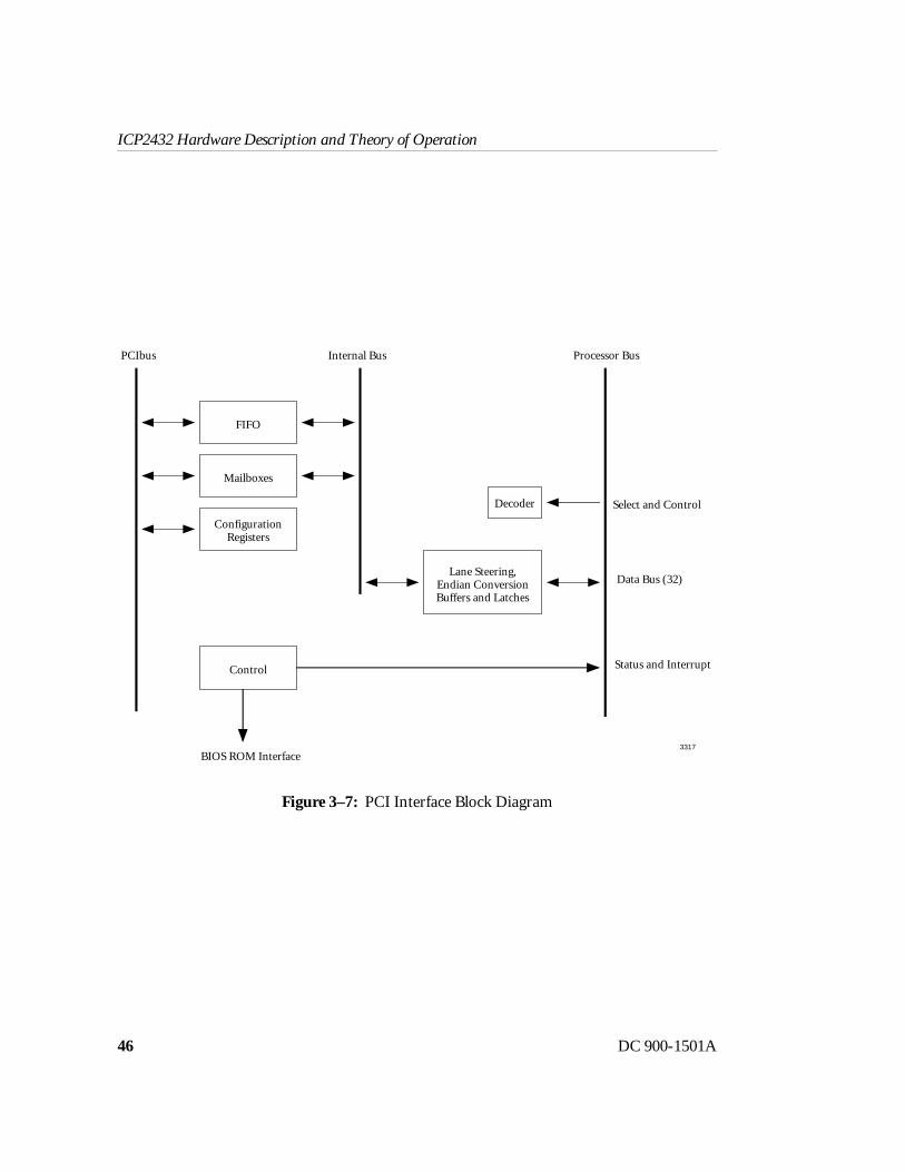
3.5 PCI Interface
The ICP2432 front-end processor may be used with any computer that has PCIbus sup-
port.
The interface comprises multiple mailbox registers and dual FIFOs. The S5933 has an
integrated DMA controller on the PCIbus side and supports the use of the 68349 DMA
channels on the add-in side. As a bus master (initiator), it supports memory read and
memory write commands. As a slave (target), it supports I/O reads/writes and configu-
ration reads/writes. Figure 3–7 shows the PCI interface block diagram.
The mailboxes are used to pass messages between the ICP and the host to coordinate
data exchange while the FIFOs are used for actual data transfer. Writing to the out-
bound mailbox from one side can generate an interrupt on the other side.
Detailed descriptions of the ICP implementation are found in Simpact’s ICP2432-to-
PCI Host Protocol Specification, DC 900-1509.
3.5.1 PCI Configuration Registers
The PCI specification defines a configuration space that all devices must support. The
S5933 provides both hard-wired and “soft” registers that are modified by the ICP2432.
The S5933 includes an interface to a serial EEROM device. At reset time, the EEROM is
used to modify the 5933’s “soft” configuration registers with ICP2432-specific parame-
ters.
46 DC 900-1501A
ICP2432 Hardware Description and Theory of Operation
Figure 3–7: PCI Interface Block Diagram
Select and Control
Data Bus (32)
Status and Interrupt
ConfigurationRegisters
FIFO
Mailboxes
Control
Lane Steering,Endian ConversionBuffers and Latches
Decoder
BIOS ROM Interface
Processor BusPCIbus
3317
Internal Bus

3: Hardware Survey
DC 900-1501A 47
The ICP2432 EEPROM modifies the 56933 registers as shown in Figure 3–8.
Figure 3–8: PCI Configuration Space Header
3429
PCI Configuration Space Header
DEVICE ID = 0002, 0004, or 0008 VENDOR ID = 12A1
STATUS COMMAND
CLASS CODE = FF0000 REV ID
BIST = 00 HEADER TYPE = 00 LATENCY TIMER = F8 CACHE LINE SIZE
BASE ADDRESS REGISTER #0 = I/O (64 bytes)
BASE ADDRESS REGISTER #1 = 0000_0000, disabled
BASE ADDRESS REGISTER #2 = 0000_0000, disabled
BASE ADDRESS REGISTER #3 = 0000_0000, disabled
BASE ADDRESS REGISTER #4 = 0000_0000, disabled
BASE ADDRESS REGISTER #5 = 0000_0000, disabled
RESERVED = 0’s
EXPANSION ROM BASE ADDRESS = 0000_0000, disabled
MAX_LAT = 0F MIN_GNT = FF INTERRUPT PIN = 1, INTA# INTERRUPT LINE
RESERVED = 0’s
RESERVED = 0’s
RESERVED = 0’s
31 24 23 16 15 8 7 00

48 DC 900-1501A
ICP2432 Hardware Description and Theory of Operation
3.6 Details of Operation
This section describes the interrupt, board timing, Z-BUS arbitration, reset, bus error,
and NMI functions of the ICP2432.
3.6.1 Interrupts
The ICP2432 implements the 68349 interrupt mechanism as described in
Section 3.6.1.1, the external interrupt level assignments as described in Section 3.6.1.2,
and the interrupt arbitration as described in Section 3.6.3.2.
3.6.1.1 Interrupt Operation
The ICP2432 uses three of the seven 68349 processor interrupt levels. Each interrupt
source accesses its own interrupt request pin (INTRQn). These input pins are sampled
by the processor. If any of them are asserted, and if the highest priority pin is greater
than the current interrupt mask level, an interrupt request is made pending. The pro-
cessor services the pending interrupt at the next instruction boundary. The 68349 sup-
ports both device-supplied vector (DSV) and autovector (AV) peripherals. The IUSCs
are DSV, and the NMI and AMCC5933 PCIbus interface are AV. When the processor is
ready to initiate interrupt servicing, it begins an interrupt acknowledge cycle. This cycle
is similar to a normal read cycle. An IACK cycle at the pending interrupt level enables
the highest priority device at that level to present a vector byte. The processor uses this
byte as an index to locate the peripheral’s interrupt service entry point.
3.6.1.2 Interrupt Level Assignments
The interrupt levels can be summarized as follows:
Level 7 A non-maskable interrupt that causes the 68349 to stop execu-
tion of the current program and break to the debugging tool.
NMIs may be issued by pushing the NMI push-button on the
optional debug module

3: Hardware Survey
DC 900-1501A 49
Level 6 Used by the integrated universal serial controllers (IUSCs)
Level 5 Used by the PCIbus interface AMCC5933
Level 4 Not used
Level 3 Not used
Level 2 Not used
Level 1 Not used
Level 0 Normal operation, no interrupts
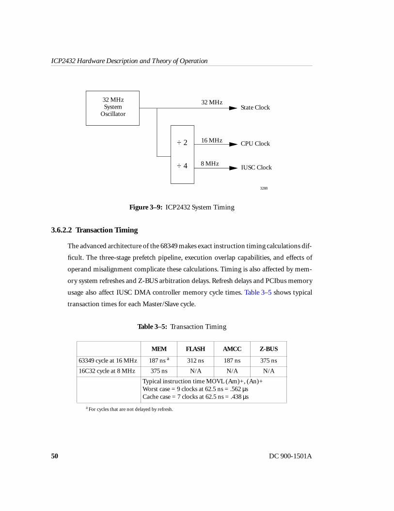
3.6.2 Timing
This section describes the clock generation logic of the ICP2432 and the transaction
timings that result from its implementation.
3.6.2.1 Clock Generation
The ICP2432 uses synchronous state machine design techniques throughout the con-
trol logic to ensure accurate circuit performance and to increase circuit reliability. All
clock signals are derived from a divider circuit that is clocked by the 32 MHz system
oscillator as shown in Figure 3–9.
The 32 MHz state clock is used by the processor bus memory controller, the Z-BUS
conversion, and arbitration state machines. The 16 MHz clock is used by the 68349
CPU and as an optional input to the IUSC. The 8 MHz clock is used by the IUSC DMA
controllers and the Z-BUS interrupt state machine.
50 DC 900-1501A
ICP2432 Hardware Description and Theory of Operation
3.6.2.2 Transaction Timing
The advanced architecture of the 68349 makes exact instruction timing calculations dif-
ficult. The three-stage prefetch pipeline, execution overlap capabilities, and effects of
operand misalignment complicate these calculations. Timing is also affected by mem-
ory system refreshes and Z-BUS arbitration delays. Refresh delays and PCIbus memory
usage also affect IUSC DMA controller memory cycle times. Table 3–5 shows typical
transaction times for each Master/Slave cycle.
a For cycles that are not delayed by refresh.
Figure 3–9: ICP2432 System Timing
Table 3–5: Transaction Timing
MEM FLASH AMCC Z-BUS
63349 cycle at 16 MHz 187 ns a 312 ns 187 ns 375 ns
16C32 cycle at 8 MHz 375 ns N/A N/A N/A
Typical instruction time MOVL (Am)+, (An)+Worst case = 9 clocks at 62.5 ns = .562 µsCache case = 7 clocks at 62.5 ns = .438 µs
32 MHzSystem
Oscillator
÷ 2
÷ 4
State Clock
16 MHz
IUSC Clock8 MHz
3288
CPU Clock
32 MHz

3: Hardware Survey
DC 900-1501A 51
3.6.3 Z-BUS Operation
The low-level hardware operation of the 68349 and IUSC devices is controlled by the
68349 bus arbiter and a bus conversion state machine. The four- and eight-port ICPs
also require interrupt arbitration and DMA arbitration state machines as described
below. Refer to Figure 3–10 on page 52.
3.6.3.1 Bus Conversion State Machine
The bus conversion state machine controls any transactions that span the processor and
the communications buses. When the 68349 accesses a device on the Z-BUS, the state
machine translates the Motorola control signals to the appropriate Z-BUS control sig-
nals and manages the multiplexing of the Motorola address and data buses onto the
multiplexed Z-BUS. When an IUSC is bus master and accesses the DRAM memory, the
state machine translates the Z-BUS control signals to the appropriate Motorola control
signals and manages the de-multiplexing of the Z-BUS address/data bus onto the sepa-
rate Motorola address and data buses. The bus conversion state machine also monitors
the 68349 interrupt and bus arbitration signals and manages the inter-bus buffers dur-
ing interrupt and bus arbitration cycles.
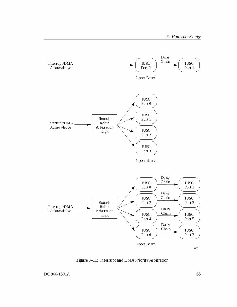
3.6.3.2 Interrupt and DMA Arbitration
The IUSC supports a daisy-chain mechanism for both its interrupt and bus request
operations. The following paragraphs discuss the interrupt request and acknowledge
operation, but are also valid for the bus request and acknowledge operation. The
descriptions of the interrupt daisy-chain and the state machine details are duplicated
for the DMA. See Figure 3–11 on page 53.
The Zilog interrupt daisy-chain implementation connects multiple IUSC devices to a
common interrupt request line. When an interrupt acknowledge cycle is started, an
interrupt enable (IEI and IEO) propagates serially through the devices. A device that
does not have an interrupt pending passes the enable to the next device in the chain.
The device at the highest physical priority on the chain, that has an interrupt pending,

52 DC 900-1501A
ICP2432 Hardware Description and Theory of Operation
Figure 3–10: Z-BUS Arbitration Block Diagram
AAAAAAAAAAAAAAAAAAAAAAAAAAAAAAAAAAAAAAAA Z-BUS Address/Data
Address Buffers
Processor Control Signals
Z-BUS Control Signals
IsolationBuffers
AAAAAAAAAAAAAAAAAAAAAAAAAAAAAAAAAAAAAAAA
Processor Address Bus
CPU CLK
AS, R/W, DTACK,
INT REQ, INTACKs
BUSREQ, BG, BGACK
ZUAS, ZAS, ZDS,
ZR/W
AAAAAAAAAA
AAAA
AAAAAA
AA
AAAAAAAAAAAAAAAAAA
AAAAAA
AAAAAAAAAA
AAAA
AAAAAA
Bus Conversion
State Machine
DMA & INTArbitration
State Machines
IUSC Devices
(2, 4, or 8)ACKs
REQsDataBuffers
3056
AAAAAAAAAAAAAAAAAAAAAAAAAAAAAAAAAAAAAAAA
Processor Data Bus
AAAAAA
AAAAA
AAAAA
AAAAAAA
AAAAA
AAAAA
AA
Enable and Direction Control
3: Hardware Survey
DC 900-1501A 53
Figure 3–11: Interrupt and DMA Priority Arbitration
IUSCPort 0
IUSCPort 1
Daisy ChainInterrupt/DMA
Acknowledge
2-port Board
4-port Board
Interrupt/DMAAcknowledge
Round-Robin
ArbitrationLogic
IUSCPort 0
IUSCPort 1
IUSCPort 2
IUSCPort 3
3428
8-port Board
Interrupt/DMAAcknowledge
Round-Robin
ArbitrationLogic
IUSCPort 0
IUSCPort 2
IUSCPort 4
IUSCPort 6
IUSCPort 1
IUSCPort 3
IUSCPort 5
IUSCPort 7
Daisy Chain
Daisy Chain
Daisy Chain
Daisy Chain

54 DC 900-1501A
ICP2432 Hardware Description and Theory of Operation
blocks the enable signal to the next device in the chain and presents its vector to the pro-
cessor for servicing.
The two baseboard ports on the two-port ICP2432 are on a single daisy-chain with
port 0 at a higher priority than port 1. The interrupt and bus requests are tied directly
to the bus control state machine and do not use a complex arbitration state machine.
On the four-port ICP2432, each IUSC has its interrupt and bus request control signals
connected to complex arbitration state machines. These machines make the request to
the 68349 and, according to the current priority, pass the acknowledge to the appropri-
ate device. Each of these state machines implements a modified round-robin algorithm.
This scheme uses a “last user = lowest priority” method that eliminates the delays asso-
ciated with true round-robin, or time-slice, schemes. When only one IUSC has a
request, the state machine acknowledges that IUSC without waiting for a time-slice
window to occur. If more than one IUSC has a request, the state machine issues a grant
according to the current IUSC priority list.
The eight-port ICP2432, interrupt and DMA arbitration comprises a combination of
the baseboard and four-port schemes. The arbitration state machines are identical to
those described for the four-port board, but each of the four levels has two daisy-
chained IUSCs as described for the two baseboard ports.
3.6.4 Reset
In normal operation, the reset controller keeps the RESET signal in a high-impedance
state. This allows the 68349 to drive the line during the execution of a reset instruction.
The reset controller PLD generates an 100 microsecond minimum reset pulse for the
following conditions:
1. At power-up
2. When the PCIbus signal RST# is asserted
3. When bit 24 of the bus master control register is set by the host
4. When the reset switch on the optional debug module is pushed
Space below in body paragraphs on this page was changed to 9 points to get item 4 in list below on the page.

3: Hardware Survey
DC 900-1501A 55
All of the devices, state machines, and configuration registers on the board are initial-
ized to a known state when the RESET signal is driven low.
3.6.5 Non-maskable Interrupt (NMI)
The interrupt request controller issues a non-maskable interrupt (NMI) request when
the NMI button on the optional debug module is pressed. The 68349 executes the code
pointed to by the AutoVector 7 vector.
3.7 I/O Port Details
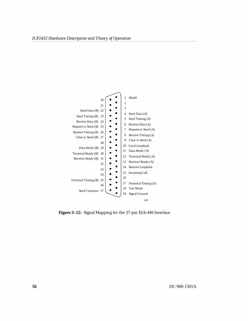
Figure 3–12 shows the signal mapping for the EIA-449 interface. Figure 3–13 shows the
signal mapping for the EIA-530 interface (which is also used for EIA-530A and
EIA-232).
The eight-port version of the ICP2432 always provides an EIA-232 electrical interface
on all ports. Figure 3–14 shows the signal mapping for the EIA-232 interface.
3.7.1 Two-port Baseboard
Each of the two ports on the baseboard use 26-pin micro-D to Dsub adapter cables
which map to standard EIA (DTE, male pin) connectors. The cable options are:
• AS-100-0185-01 = EIA-530 (25-pin) connector
• AS-100-0186-01 = EIA-449 (37-pin) connector
• AS-100-0185-01 + AS-000-283-01 = V.35 (34-pin) connector
3.7.2 Four-port Mezzanine Board
The four-port mezzanine board provides four full-function, software-programmable
EIA interface ports, as described for the two baseboard ports except that the four-port
mezzanine board uses a high-density 100-pin connector (similar to those used in SCSI
56 DC 900-1501A
ICP2432 Hardware Description and Theory of Operation
Figure 3–12: Signal Mapping for the 37-pin EIA-449 Interface
3295
21
23
24
26
27
28
30
22
25
29
31
202
4 Send Data (A)
5 Send Timing (A)
7 Request to Send (A)
8 Receive Timing (A)
9 Clear to Send (A)
11 Data Mode
3
6 Receive Data (A)
10 Local Loopback
12 Terminal Ready (A)
1 Shield
Receiver Ready (A)1332
33
34
36
35
37
Send Timing (B)
Receive Data (B)
Receive Timing (B)
Clear to Send (B)
Terminal Ready (B)
Send Data (B)
Request to Send (B)
Data Mode (B)
Receiver Ready (B)
Terminal Timing (B)
Send Common
14 Remote Loopback
15 Incoming Call
17 Terminal Timing (A)
16
18 Test Mode
Signal Ground19
(A)

3: Hardware Survey
DC 900-1501A 57
Figure 3–13: Signal Mapping for the 25-pin EIA-530 Interface
Figure 3–14: Signal Mapping for the 25-pin EIA-232 Interface
3294
Transmitter Signal Element Timing DCE (A) 15
Receiver Signal Element Timing DCE (A) 17
Local Loopback 18
DTE Ready (A) 20
Remote Loopback 21
DCE Ready (B) 22
Transmitter Signal Element Timing DTE (A) 24
16Received Data (B)
19Request to Send
23DTE Ready (B)
25Test Mode
14Transmitted Data (B)2 Transmitted Data (A)
4 Request to Send (A)
5 Clear to Send (A)
7 Signal Ground
8 Received Line Signal Detector (A)
9 Received Signal Element Timing DCE (B)
11 Transmitter Signal Element Timing DTE (B)
3 Received Data (A)
6 DCE Ready (A)
10 Received Line Signal Detector (B)
12 Transmitter Signal Element Timing DCE (B)
1 Shield (A)
Clear to Send (B)13
3293
DCE Transmitter Signal Element Timing 15
Receiver Signal Element Timing 17
Local Loopback 18
Data Terminal Ready 20
21
Ring Indicator 22
DTE Transmitter Signal Element Timing 24
16
19
23
25
142 Transmitted Data
4 Request to Send
5 Clear to Send
7 Signal Ground
8 Received Line Signal Detector
9
11
3 Received Data
6 Data Set Ready
10
12
1 Protective Ground
13

58 DC 900-1501A
ICP2432 Hardware Description and Theory of Operation
interfaces) for the I/O ports. The following “quadrapus” cable options are available
which map the 100-pin connector to four standard EIA (DTE, male pin) connectors:
• AS-100-0194-01 = four EIA-530 (25-pin) connectors
• AS-100-0195-01 = four EIA-449 (37-pin) connectors
• AS-100-0194-01 + four AS-000-283-01 = four V.35 (34-pin) connectors
3.7.3 Eight-port Mezzanine Board
The eight-port mezzanine board provides eight full-function EIA-232 ports. The ports
are EIA-232 only; they are not software configurable to other electrical interfaces.
The eight-port mezzanine board uses a high-density 100-pin connector (similar to
those used in SCSI interfaces) for the I/O ports. The following “octopus” cable maps the
100-pin connector to eight standard EIA (DTE, male pin) connectors.
• AS-100-0193-01 = eight EIA-23 (25-pin) connectors
DC 900-1501A 59
Index
Numerics
68349block diagram 31integrated processor 30power-up defaults 34
A
ArbitrationDMA 51interrupt 51
Architecturedual bus 23overview 20PCI interface 25
Audience 11
B
Baseboard 55Block diagrams
68349 processor 31ICP2432 24PCI interface 46Z-BUS arbitration 52
Board ID register 44Bus conversion state machine 51
C
Cacheconfigurable instruction 32
Chip select registers 36Circuits 42
receive 42transmit 42
Clock generation 49
Clock steering 43Communications bus, see Z-BUSCommunications devices 40Communications traffic 22Configurable instruction cache 32Conventions, document 12CPU32+ processor 32Customer support 13
D
Debug moduleto ICP 39to terminal 39
Debug port 38Device parameters 36Devices, communication 40Diagnostics
FLASH 37DMA
arbitration 51module 33
Document conventions 12Downloader
FLASH 38DRAM 36Dual-bus architecture 23
E
EIA-232 signal mapping 57EIA-449 signal mapping 56EIA-530 signal mapping 57Equipment, required 11
F
FLASH 37

60 DC 900-1501A
ICP2432 Hardware Description and Theory of Operation
diagnostics 37downloader 38
H
Hardware survey 23History of revisions 13
I
ICPapplications 17architecture
dual bus 23benefits 16block diagram 24features 16purpose 15
ID register 44Interface
PCI 25, 45International Standards Organization (ISO) 17Interrupt arbitration 51Interrupts 48
level assignments 48non-maskableoperation 48
I/O port details 55ISO OSI
reference model 17IUSC Configuration 41
M
Memorynon-volatile 25peripheral space 25processor bus 36volatile 28Z-BUS 28
Memory map 25ICP 26processor bus 27Z-BUS 29
Memory module, quad data 32Mezzanine boards
eight-port 58four-port 55
Mode input register 43Mode select register 44Modules
DMA 33serial 33system integration 34
N
NMI, see non-maskable interruptNon-maskable interrupt 55Non-volatile memory 25
O
Open system interconnection (OSI) 17Operation 48
application environment 22routine 21
Overview 15
P
PCIconfiguration registers 45interface 25, 45interface block diagram 46
Peripheral devicesZ-BUS 28
Peripheral space 25Peripherals
on-chipDMA module 33serial module 33system integration module 34
Ports 22Processor bus 30
68349 30flash 37memory 36memory map 27non-volatile memory 37
Productsupport 13
Q
Quad data memory module 32

Index
DC 900-1501A 61
R
Receive circuits 42Reference documents 12Registers
board ID 44chip select 36PCI configuration 45Sipex mode select 44test mode input 43
Reserved space 28Reset 21, 54Revision history 13
S
Serial module 33Signal mapping
EIA-232 57EIA-449 56EIA-530 57
Sipex mode select register 44Startup 21Support, product 13System
configuration 35integration module 34protection 35timing 50
T
Technical support 13Test mode input register 43Timing 49
clock generation 49transaction 50
Transaction timing 50Transmit circuits 42
V
Volatile memory 28
X–Z
Z-BUSarbitration
block diagram 52circuits 42
communication devices 40memory 28memory map 29operation 51peripheral devices 28

62 DC 900-1501A
ICP2432 Hardware Description and Theory of Operation

ICP2432 Hardware Descriptionand Theory of Operation
DC 900-1501A
Customer Report Form
We are constantly improving our products. If you have suggestions or problems you would
like to report regarding the hardware, software or documentation, please complete this form
and mail it to Simpact at 9210 Sky Park Court, San Diego, CA 92123, or fax it to
(619) 560-2838.
If you are reporting errors in the documentation, please enter the section and page number.
Your Name:
Company:
Address:
Phone Number:
Product:
Problem or
Suggestion:

Simpact, Inc.Customer Service
9210 Sky Park CourtSan Diego, CA 92123


![BY ANDREW T. MILLER AND PETER K. ALLENallen/PAPERS/graspit.final.pdf · 2005. 1. 17. · MATLAB [6], RoboSiM [7], and Simpact [8], but none of these focus on the grasping problem](https://img.pdfslide.us/doc/110x75/5fef4560e97c735bcb767643/by-andrew-t-miller-and-peter-k-allen-allenpapersgraspitfinalpdf-2005-1.jpg)