Embed Size (px)
Citation preview

E DWAR D JON E S-I M HOTE P∗
Icons and Electronics
ABSTRACT
In the late 1950s, a wide-ranging debate erupted over the seemingly innocuous questionof how transistors—the revolutionary new electronic devices—should be drawn. By forc-ing a break in the long-standing traditions of electronic drawing, transistors generateda crisis in the ontology of circuit diagrams, forcing a choice between representationsthat emphasized form and those that stressed function. This paper explores what wasat stake in that mid-century debate over visual culture. It tracks one function-basedsymbol through concerns about auto-comprehension, visual communication, and elec-tronic reliability to see how transistor symbols formed crucial sites for articulating themeanings of material devices and their relationship to the wider populations of elec-tronic entities, especially vacuum tubes. In doing so, the article shifts the emphasis inthe history of electronics from material to visual culture, recasting our understandingof postwar electronics as a history of drawings as well as devices.
K EY WO R D S : Electronics, visual culture, transistors, symbols, vacuum tubes, historiography,schematic diagrams
I NTROD UCTION
In early October 1957, an émigré British electrical engineer named Norman
Moody addressed a small audience of physicists and engineers gathered at
CERN, the newly built high-energy physics laboratory straddling the French-Swiss
| 4 0 5
*Science and Technology Studies, York University, Bethune College 218, 4700 Keele Street,
Toronto ON M3J 1P3, Canada; [email protected].
The following abbreviations are used: DRTE, Defence Research Telecommunications Estab-
lishment; IRE, Institute of Radio Engineers; NAC, National Archives of Canada, Ottawa, Canada;
RAF, Royal Air Force; RCA, Radio Corporation of America; RG, Record Group; RPL, Radio
Physics Laboratory; TP, Phillip Thompson Personal Files, Ottawa, Canada; TRE, Telecommu-
nications Research Establishment; WW, Wireless World.
Historical Studies in the Natural Sciences, Vol. 38, Number 3, pps. 405–450. ISSN 1939-1811, elec-
tronic ISSN 1939-182X. © 2008 by the Regents of the University of California. All rights reserved.
Please direct all requests for permission to photocopy or reproduce article content through the Univer-
sity of California Press’s Rights and Permissions website, http://www.ucpressjournals.com/reprintinfo.
asp. DOI: 10.1525/hsns.2008.38.3.405.
HSNS3803_03 7/10/08 5:58 PM Page 405

border. Moody had been invited as part of a small group of specialists to dis-
cuss the best methods for generating data from the increasingly gargantuan ma-
chines of high-energy physics. With the material culture of particle physics split
between the image-based traditions of the bubble chamber on the one hand,
and the logic-based tradition of coincidence circuits and statistical analyses on
the other, Moody’s allegiances must have seemed clear. His own expertise was
in pulse triggers and counting circuits, developed as he rose (with no univer-
sity degrees or formal training) through Depression-era television design, wartime
radar circuitry, and postwar atomic weapons and nuclear engineering. Now the
head of a defense electronics laboratory outside Ottawa, he had come to ad-
dress an altogether different divide in twentieth-century material culture—one
with implications stretching far beyond the image- or logic-based machines of
high-energy physics.
Cutting across the material divisions between bubble chambers and coinci-
dence circuits had been an engineering culture built around evacuated tubes—
Geiger-Müller counters and photomultiplier tubes, which formed the basis of
counting circuits, but also the ubiquitous vacuum tubes, which drove the out-
put of logic-based devices and helped automate the analysis of bubble cham-
ber images.1 Moody was there to propose how engineers and physicists might
begin breaking their long-standing relationship to vacuum tubes and start cul-
tivating a new one in its place.
His talk, “The Present State of the Transistor and its Associated Circuit Art,”
began with a warning. If deployed properly—artfully—the transistor could
prove to be more reliable than the vacuum tube. Deployed incorrectly, how-
ever, the results could be disastrous. As if to enliven the language of art in his
presentation, Moody placed iconography at its core. In a move riddled with
irony (given his audience), the electrical engineer began a talk consumed by
logic circuits with an assertion about the primacy of images: the first step toward
making transistors reliable, Moody suggested, was to change the way they were
drawn.2 It is that remarkable assertion—that making transistors reliable meant
drawing them differently—that motivates this paper.
Moody’s comment is startling because of the way it makes the proper func-
tioning of transistors depend not on the materiality of the devices, but on their
4 0 6 | J O N E S - I M H OT E P
1. For more on image- and logic-based traditions, see Peter Galison, Image and Logic: A Mate-rial Culture of Microphysics (Chicago: University of Chicago Press, 1997), esp. chaps. 1, 2, and 6.
2. N. F. Moody, “The Present State of the Transistor and its Associated Circuit Art,” NuclearInstruments 2 (1958): 182–92, on 182–83.
HSNS3803_03 7/10/08 5:58 PM Page 406

I C O N S A N D E L E C T R O N I C S | 4 0 7
representation. That shift in emphasis—from the details of devices to the intri-
cacies of drawings—destabilizes a view of transistors (and electronics generally)
that already enveloped the devices in the late 1950s, and which has dominated
historical writing about them ever since.3 On this view, making transistors work
was ultimately about getting the material details just right—tapping crystal
“hot spots,” managing impurities, slicing gold foil just thin enough, growing
oxide layers just thick enough to transform elusive quantum-mechanical phe-
nomena into robust semiconductor actions. “Dirt effects,” Wolfgang Pauli de-
clared them, as if to certify their grubby materiality.
The consequences were dramatic. By making transistor action reliable,
the story goes, those details and their refinements made possible the defin-
ing material break in twentieth-century electronics—the central organizing
rupture, as machine after machine gradually saw the fragile evacuated glass
of the vacuum tube yield to rugged semi-conducting crystals, ultimately
3. One approach to the history of transistors has stressed the material transformations needed
to create and recreate the devices, as a corrective to the emphasis on conceptual breakthroughs.
See, for example, Christophe Lécuyer, Making Silicon Valley: Innovation and the Growth of HighTech (Cambridge, MA: MIT Press, 2005); Ross Knox Bassett, To the Digital Age: Research Labs,Start-up Companies, and the Rise of MOS Technology (Baltimore, MD: Johns Hopkins University
Press, 2002); Hyungsub Choi, “The Boundaries of Industrial Research: Making Transistors at
RCA, 1948–1960,” Technology and Culture 48 (2007): 758–82. For a fascinating discussion of the
problems of production, and the role of workers, see Stuart W. Leslie, “Blue Collar Science: Bring-
ing the Transistor to Life in the Lehigh Valley,” Historical Studies in the Physical and Biological Sci-ences 32, no. 1 (2001): 71–113. For the emphasis on conceptual breakthroughs, see John Peter
Collet, “The History of Electronics: From Vacuum Tubes to Transistors,” in Science in the Twen-tieth Century, ed. John Krige and Dominique Pestre (London: Routledge, 1997), 253. For this view
in relation to the transistor, see Lillian Hoddeson, “Research on Crystal Rectifiers During World
War II and the Invention of the Transistor,” History and Technology 11 (1994): 121–30; Lillian Hod-
deson, “The Discovery of the Point-Contact Transistor,” Historical Studies in the Physical Sciences12 (1981): 41–76; Lillian Hoddeson and Michael Riordan, Crystal Fire: The Birth of the Informa-tion Age (New York: W. W. Norton & Company, 1997); Ernest Braun, “Selected Topics from the
History of Semiconductor Physics and its Applications,” in Out of the Crystal Maze: Chapters inthe History of Solid State Physics, ed. Lillian Hoddeson, Ernest Braun, Jürgen Teichmann, and
Spencer Weart (New York: Oxford University Press, 1992), 443–88; Charles Weiner, “How the
Transistor Emerged,” IEEE Spectrum 10 (1973): 24–33. Riordan and Hoddeson have also suggested
that material devices gave “operational reality” to theoretical entities, like the electron or the hole.
See Michael Riordan and Lillian Hoddeson, “The Electron, the Hole, and the Transistor,” in
Histories of the Electron: The Birth of Microphysics, ed. Jed Z. Buchwald and Andrew Warwick
(Cambridge: MIT Press, 2001), 327–38. For a contrasting view on the development of the tran-
sistor, see M. Gibbons and C. Johnson, “Science, Technology and the Development of the Tran-
sistor,” in Science in Context: Readings in the Sociology of Science, ed. Barry Barnes and David
Edge (Cambridge: MIT Press, 1982), 177–85.
HSNS3803_03 7/10/08 5:58 PM Page 407

4 0 8 | J O N E S - I M H OT E P
enabling the micro-miniature, high-speed, and highly dependable electron-
ics of today.4
That focus on materials and devices has been crucial in helping us under-
stand the origins of the transistor, its deep moorings in materials science and the
quantum theory of metals, and its role in transforming electronic material cul-
ture at mid-twentieth century. If taken too far, however, the approach threatens
to obscure a more complex and, I think, more interesting history—one rooted
in a key irony. Throughout the 1950s, technologists were able to agree wholly
on the material details of transistors and on the physics that drove the devices,
and yet disagree simultaneously and fiercely about what transistors were and
how they functioned.5 By collapsing those multiple meanings of the devices
into a unitary material identity, materialist histories obscure the sources and
the stakes of those disagreements. They ultimately tell us little about how
and why technologists learned to think differently about transistors, to un-
derstand them as electronic entities, and therefore to put them to work.6
4. On the role of production techniques in making the transistor reliable, see Christophe
Lécuyer, “Silicon for Industry: Component Design, Mass Production, and the Move to Com-
mercial Markets at Fairchild Semiconductor, 1960–1967,” History and Technology 16 (1999): 179–216,
esp. 188–91; Ernest Braun and Stuart Macdonald, Revolution in Miniature: The History and Im-pact of Semiconductor Electronics, 2nd ed. [1978], (Cambridge: Cambridge University Press, 1982);
Riordan and Hoddeson, Crystal Fire (ref. 3), esp. chap. 10; and Ross Knox Bassett, To the DigitalAge: Research Labs, Start-up Companies and the Rise of MOS Technology (Baltimore, MD: Johns
Hopkins University Press, 2007). On the role of the military, particularly in the context of minia-
turization, see Thomas J. Misa, “Military Needs, Commercial Realities, and the Development of
the Transistor, 1948–1958,” in Military Enterprise and Technological Change: Perspectives on theAmerican Experience, ed. Merrit Roe Smith (Cambridge: MIT Press, 1985), 253–88. The use of the
transistor as a periodization tool is common. See, for instance, Collet, “History of Electronics”
(ref. 3), 254; on its role in the shift from modern mass culture to postmodern information cul-
ture, see Hoddeson and Riordan, “Electron” (ref. 3), 336.
5. Trevor Pinch and Wiebe Bjiker have discussed the multiple meanings of singular artifacts
through their concept of “relevant social groups”; see Pinch and Bijker, “The Social Construc-
tion of Facts and Artifacts: or How the Sociology of Science and the Sociology of Technology
Might Benefit Each Other,” Social Studies of Science 14 (1984): 399–441. I use symbols to explore
those multiple meanings without suggesting that users of a given symbol formed a monolithic
group.
6. Bruce Hevly has suggested that learning to use the devices ought to be part of any history
of the transistor; Hevly, review of Revolution in Miniature, by Braun and Macdonald (ref. 4), Tech-nology and Culture 25 (1984): 882–83. More generally, Ruth Schwartz Cowan has focused on the
users of artifacts as a way of arriving at “properly constituted” histories of technology; Ruth
Schwartz Cowan, “The Consumption Junction: A Proposal for Research Strategies in the Soci-
ology of Technology,” in The Social Construction of Technological Systems: New Directions inthe Sociology and History of Technology, ed. Wiebe Bjiker, Thomas Hughes, and Trevor Pinch
(Cambridge, MA: MIT Press, 1987), 261–80.
HSNS3803_03 7/10/08 5:58 PM Page 408

I C O N S A N D E L E C T R O N I C S | 4 0 9
Moody, working in the thick of these debates, points us to that more com-
plicated and more complete history. Speaking at the tail-end of a soon-to-be-
forgotten debate over drawing, he suggested that the key to making transis-
tors work lay not in conduction bands or advanced doping techniques, but in
symbols. It is that move from the bulky material devices of mid-century elec-
tronics to their abstracted line drawings—from material culture to visual cul-
ture—that I explore here.
The symbol that animated Moody’s discussion was part of an explosion of
competing schemes for transistors: in the mid-1950s at least fifteen public pro-
posals and countless more private initiatives swept across electronics journals,
engineering schematics, sketch-pads, and blackboards.7 Driving that explosion
was a seemingly simple question: how should transistors be drawn? The act of
drawing and the place of diagrams has been a lively topic in science studies for
two decades now.8 Within the history of technology, it has been central to his-
tories of mechanical engineering, highlighting, for instance, connections be-
tween uniform production, mechanical drawing, and the emergence of the
modern state; or detailing how the rise of drafting helped draw the boundary
between the modern and pre-modern worlds.9 Those issues, however, have been
almost completely absent from the history of electronics and electrical engi-
neering. Historical and technical writings alike have treated competing circuit
7. I am grateful to David Hounshell for bringing to my attention the existence of these pri-
vate schemes in the U.S.
8. For a fascinating discussion of diagrammic representation in scientific pedagogy and train-
ing, see David Kaiser, Drawing Theories Apart: The Dispersion of Feynman Diagrams in PostwarPhysics (Chicago: University of Chicago Press, 2005); and a more general discussion of pedagogy
in David Kaiser, ed., Pedagogy and the Practice of Science: Historical and Contemporary Perspectives(Cambridge, MA: MIT Press, 2005). More generally, see Bruno Latour and Steve Woolgar, Lab-oratory Life: The Construction of Scientific Facts, 2nd ed. [1979] (Princeton: Princeton University
Press, 1986), 51, 89, and 245; Michael Lynch and Steve Woolgar, eds., Representation in ScientificPractice (Cambridge: MIT Press, 1990); Martin Rudwick, “The Emergence of a Visual Language
for Geological Science, 1760–1840,” History of Science 14 (1976): 149–95; Caroline Jones and Peter
Galison, eds., Picturing Science, Producing Art (New York: Routledge, 1998); Brian Baigrie, Pic-turing Knowledge: Historical and Philosophical Problems Concerning the Use of Art in Science (Toronto:
University of Toronto Press, 1996); Luc Pauwels, ed., Visual Cultures of Science: RethinkingRepresentational Practices in Knowledge Building and Science Communication (Lebanon, NH:
University Press of New England, 2005).
9. Ken Alder, “Making Things the Same: Representation, Tolerance and the End of the An-cien Régime in France,” Social Studies of Science 28 (1998): 499–545; David McGee, “From Crafts-
manship to Draftsmanship: Naval Architecture and the Three Traditions of Design,” Technologyand Culture 40 (1999): 209–36. For a more general discussion of “visual thinking” in engineer-
ing, see Eugene Ferguson, Engineering and the Mind’s Eye (Cambridge, MA: MIT Press, 1992).
HSNS3803_03 7/10/08 5:58 PM Page 409
4 1 0 | J O N E S - I M H OT E P
symbols, if they have treated them at all, as deviations and curiosities to be
swept away by an inevitable standardization.10 In the process, they have ignored
issues of representation when writing the history of a discipline that, like few
others, uses icons in order to think.
That oversight masks broader issues. For technologists in the 1950s, the seem-
ingly simple question of how transistors should be drawn entailed other, deeper
concerns: How should workers be commanded? What dangers arose as line
drawings morphed into dense, recalcitrant artifacts? What knowledge, if any,
should symbols presume, and what should they embody? How were transis-
tors related to the wider population of electronic devices, and how might sym-
bols capture those relationships? And, not least, could engineers be trusted? Po-
sitioned at the very core of the visual culture of electronics, circuit symbols
made those questions both pressing and public. They formed the contested
ground in debates over what transistors were, what drawings ought to be, and
what practices might make both reliable.
This paper explores what was at stake in drawing transistors in the mid-
1950s. It argues that for Moody and his contemporaries, transistor symbols
were instruments crucial to making sense of the new devices. These symbols
helped express what kinds of electronic entities transistors were, and, in par-
ticular, what relationship they bore to vacuum tubes. We take that relation-
ship largely for granted now, but in the 1950s it was still in flux, and symbols
formed one of the primary means of articulating it. This paper focuses on
how a specific form of transistor, the junction transistor, sparked a crisis in
the nature of schematic diagrams. By severing the long-standing link between
macrophysical form and electronic function in these drawings—a link vouch-
safed by the vacuum tube—the new transistors gave rise to two competing
views of what transistor icons should represent, each slightly incongruent
with established forms of drawing electronics. A material-structuralist view
sought to emphasize material composition and structure within a tradition
of representation where materials did not otherwise matter; a competing
functionalist approach aimed to suggest how transistors worked in a graphic
universe dominated by suggestions of physical form. This, in turn, caused
10. The literature on the history of transistors is almost completely silent on the issue of sym-
bols. Riordan and Hoddeson’s Crystal Fire (ref. 3) makes no mention of competing schemes. Linda
Petiot goes further than most in acknowledging the existence of different conventions in her ex-
cellent study of Moody’s computer research, but she does not discuss its significance. See Petiot,
“Dirty Gertie: The DRTE Computer,” IEEE Annals of the History of Computing 16 (1994): 43–52.
HSNS3803_03 7/10/08 5:58 PM Page 410
I C O N S A N D E L E C T R O N I C S | 4 1 1
an explosion of possible symbols, as the idioms of classical design strained
under the tension between structure and function. The symbols at the core
of Moody’s CERN presentation initially emerged from that functionalist im-
pulse. As they were appropriated by different members of Moody’s group,
their meaning shifted, shaped each time by different visions of how schematic
diagrams functioned: as taxonomical expressions, as social texts, or as heuris-
tic devices.
The various sections of the paper are organized according to those under-
standings and the context in which they took shape. The paper begins with
the symbols’ initial development by Phillip Thompson, a physicist working
in the Transistor Section of Moody’s laboratory. The symbols emerged from
Thompson’s attempt to capture visually the essence of transistor action by
drawing on the existing symbols for crystal diodes. The new diode-based sym-
bols soon became the basis of a graphical nomenclature, a taxonomy of semi-
conductor symbols that embodied functional relations through iconography.
The paper goes on to locate the symbols within a changing ontology of elec-
tronic drawings and the emerging conflict between structural and functional
representation. Under attack from a competing approach that saw vacuum
tubes as the functional analogue of transistors, the symbols were quickly rein-
terpreted as part of a circuit grammar that saw schematic diagrams as com-
municative devices. Here, the building blocks of the original symbol became
syntactical elements governed by rules of composition that ensured the final
diagrams’ coherence and intelligibility. The second section of the paper ex-
amines this new role of the symbols and their importance in the changing
modes of producing electronics during the Cold War. It then turns from the
functioning of diagrams to the functioning of machines. It situates the final
interpretation of the symbols within a broader crisis in electronic reliability
during the 1950s, fueled by concerns over the agency and influence of engi-
neers and circuit designers. Fearing that conceptual and visual analogies be-
tween the transistor and the vacuum tube would lead to costly and even fatal
errors, Moody reinterpreted the diode-based symbol as a way to discipline and
guide the otherwise fallible mind of the engineer. The transistor symbol that
initially emerged from concerns over comprehension and taxonomy now be-
came a way to break the misguided and dangerous links between vacuum tubes
and transistors, links that clouded the reasoning of new engineers and plagued
the electronic schematics of the early Cold War. The paper ends with some
conclusions about what visual culture can tell us about the history of elec-
tronics during the mid-twentieth century.
HSNS3803_03 7/10/08 5:58 PM Page 411
4 1 2 | J O N E S - I M H OT E P
U N D E R STAN D I NG TRAN S I STOR S
Moody’s comments at CERN in the fall of 1957 had their origins in a series of
curious drawings that began appearing in the Electronics Laboratory of the
Canadian Defence Research Telecommunications Establishment (DRTE) in
early 1954. Formed just months after the start of the Korean War, DRTE brought
together two existing laboratories—one in radio physics, the other in elec-
tronics—to create an organization capable of addressing the growing telecom-
munications needs of the Cold War, including radio communication to the
strategically crucial Canadian North. While the Radio Physics Laboratory
launched investigations of ionospheric storms and high-frequency radio black-
outs, the Electronics Laboratory provided electronic support, initially designing
and constructing radio physics instruments, and later mounting what officials
termed “anticipatory research” into military electronics—investigations of ad-
vanced communications, electronic countermeasures, missile guidance, digital
computing, and, eventually, space technology.11
In 1954, the Laboratory created a special Transistor Section, headed by
Norman Moody, to investigate the newly developed junction transistor, the
more useful successor to the original point-contact transistor invented at Bell
Laboratories in late 1947. The new section’s aim was to develop circuit tech-
niques that built on the transistor’s unique properties—rather than using
transistors “as if they were another kind of vacuum tube.”12 The section’s
first recruit was Philip Thompson. Trained as a physicist at Cambridge Uni-
versity in the early 1940s, Thompson had passed the Natural Science Tripos
at the end of the war, then moved to Liverpool’s Automatic Telephone and
Electric, Salford Electrical Instruments (where he designed a radio altimeter
for the Royal Air Force), and finally the Radio Section of the Cavendish Lab-
oratory, where he designed instruments for the Laboratory’s research in ionos-
pheric physics. Thompson had continued this work in 1950 when he joined
the Electronics Laboratory and headed a team of technologists designing in-
strumentation for radio propagation studies in the Canadian Arctic. As his
focus shifted to transistors in 1954, Thompson saw the problem of grasping
the transistor’s unique circuit characteristics as a problem of understanding
the physics that drove them.
11. Frank T. Davies, “Actual Lecture Memos” (n.d.), Frank T. Davies Papers, Communica-
tions Research Centre, Ottawa, Canada, p. 4.
12. Philip Thompson, correspondence with the author, 10 Jun 2007.
HSNS3803_03 7/10/08 5:58 PM Page 412
I C O N S A N D E L E C T R O N I C S | 4 1 3
Junction transistors had been conceived as alternating layers of P- and N-type
semiconductors suitably arranged so that they created the microelectronic
conditions that made current amplification possible. Thompson quickly saw
that the key to transistor action did not lie in the monolithic semiconductor lay-
ers themselves, but in the micromillemetric border regions where the different
materials met. Focusing on these junctions, Thompson observed that individ-
ual P-N junctions acted like rectifiers, restricting current flow in one direction
and privileging it in the other. (Indeed, a semiconductor rectifier, or diode, was
simply a single P-N junction.) With sufficient voltage applied to the interme-
diate region, two such junctions placed close enough to each other would set
up electrical potentials that allowed electrons to spill over one junction and then
pour over the electrical potential at the next, creating amplification. Seizing on
junctions in this way, Thompson believed he could reduce the action of the tran-
sistor to the arrangement and action of its constituent junctions.
Preferring to picture physical processes in his work, Thompson casually
shifted his attention from the workings of the transistor to its symbol.13 The
most commonly used symbol for junction transistors had been borrowed from
the original point-contact devices. These suggested nothing about the existence
of junctions, much less their action. Thompson now set out to find a new way
of drawing transistors that made the junctions central and explicit. He ap-
proached the problem of representation through a simple graphic synecdoche:
from the point of view of its physics, a semiconductor device was its P-N
junctions, so the problem of representing a transistor reduced to the problem
of representing its specific arrangement of junctions. But how must the junc-
tion itself be represented? The simplest of all semiconductor devices relying on
P-N junctions was the diode—a single junction used to “rectify” current flow.
By transforming the traditional icon for the diode into a symbol for a P-N junc-
tion, Thompson could combine diode symbols to represent not only the back-
to-back arrangement of junctions in transistors, but any arrangement of P-N
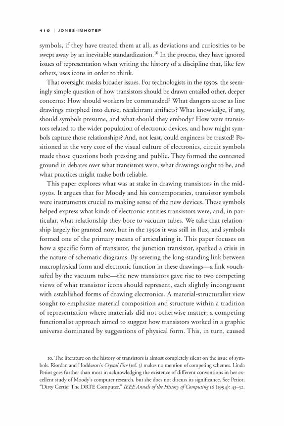
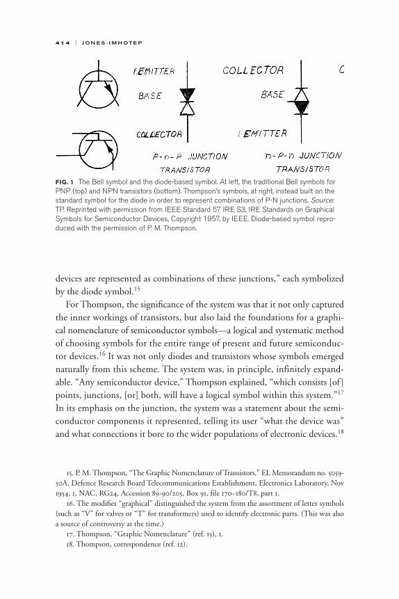
junctions used in semiconductor devices (Fig. 1).14 In a memorandum explaining
the system to his colleagues on the Transistor Panel, Thompson elaborated the
scheme: “As a diode consists of a single P-N junction in a semiconductor, a
junction transistor two such junctions, and a compound transistor several, these
13. Ibid.
14. An icon is a signifier, the form of which directly reflects the thing it signifies. A symbol,
by contrast, relies not on direct visual resemblance, but on suggestion or conventional relation.
The icon for the semiconductor diode was in fact a schematized drawing of the device itself.
HSNS3803_03 7/10/08 5:58 PM Page 413
4 1 4 | J O N E S - I M H OT E P
devices are represented as combinations of these junctions,” each symbolized
by the diode symbol.15
For Thompson, the significance of the system was that it not only captured
the inner workings of transistors, but also laid the foundations for a graphi-
cal nomenclature of semiconductor symbols—a logical and systematic method
of choosing symbols for the entire range of present and future semiconduc-
tor devices.16 It was not only diodes and transistors whose symbols emerged
naturally from this scheme. The system was, in principle, infinitely expand-
able. “Any semiconductor device,” Thompson explained, “which consists [of ]
points, junctions, [or] both, will have a logical symbol within this system.”17
In its emphasis on the junction, the system was a statement about the semi-
conductor components it represented, telling its user “what the device was”
and what connections it bore to the wider populations of electronic devices.18
15. P. M. Thompson, “The Graphic Nomenclature of Transistors,” EL Memorandum no. 5059-
50A, Defence Research Board Telecommunications Establishment, Electronics Laboratory, Nov
1954, 1, NAC, RG24, Accession 89-90/205, Box 91, file 170–180/T8, part 1.
16. The modifier “graphical” distinguished the system from the assortment of letter symbols
(such as “V” for valves or “T” for transformers) used to identify electronic parts. (This was also
a source of controversy at the time.)
17. Thompson, “Graphic Nomenclature” (ref. 15), 1.
18. Thompson, correspondence (ref. 12).
FIG. 1 The Bell symbol and the diode-based symbol. At left, the traditional Bell symbols forPNP (top) and NPN transistors (bottom). Thompson’s symbols, at right, instead built on thestandard symbol for the diode in order to represent combinations of P-N junctions. Source:TP. Reprinted with permission from IEEE Standard 57 IRE S3, IRE Standards on GraphicalSymbols for Semiconductor Devices, Copyright 1957, by IEEE. Diode-based symbol repro-duced with the permission of P. M. Thompson.
HSNS3803_03 7/10/08 5:58 PM Page 414

I C O N S A N D E L E C T R O N I C S | 4 1 5
Through Thompson’s scheme, circuit designers would peer past the surface
appearance of the devices to the fundamental P-N junctions that governed
their behavior, determined their circuit characteristics, and defined them as
electronic parts.
FOR M S AN D FU NCTION S:
D RAWI NG S AN D TH E ONTOLOG I E S OF E LECTRON ICS
Thompson and his group became the principal users of transistors in Canada
in the early 1950s, and the diode-based symbol quickly became the accepted
standard for drawing the devices in circuit diagrams throughout the Canadian
defense establishment. But already in late 1954, as the new symbols were be-
ginning to delineate secret amplifier circuits and radar systems at the Electronics
Lab, rival schemes began appearing publicly in lectures, conference presenta-
tions, classrooms, and trade publications. At least two sets of concerns (one
general, one specific) seem to have driven the proliferation. The general prob-
lem was a growing anxiety over circuit diagrams, also known as schematics—
What were they? How did they carry out their functions? What norms should
they follow? I will deal with these questions in the next section. The second,
more specific, concern emerged from a break that transistors caused in the id-
ioms of classical circuit drawing itself.
Much has been written about how transistors transformed the material culture
of postwar electronics.19 Much less has been written about how technologists’
engagement with transistors shaped norms of representation and practices of
circuit design and electrical engineering. In his classic study of mechanical en-
gineering in ancien régime France, Ken Alder speaks of the “thickness” of de-
vices, by which he means two things: a “thickness” of the artifacts, the diffi-
culty of shaping recalcitrant matter into a working device or into physically
identical copies; and a “thickness” in their representations, “the related chal-
lenge of assimilating ordinary artifacts to any idealized representation in such
a way that their qualities can be captured in their entirety.”20
19. See, for instance, Hoddeson and Riordan, Crystal Fire (ref. 3); Braun and Macdonald, Rev-olution in Miniature (ref. 4); Misa, “Military Needs” (ref. 4). As Ross Bassett notes, the term “rev-
olution” is pervasive in discussions about the impact of the transistor. See Bassett, “Digital Age”
(ref. 4), 2.
20. Alder, “Making Things the Same” (ref. 9), 503.
HSNS3803_03 7/10/08 5:58 PM Page 415
4 1 6 | J O N E S - I M H OT E P
Electronics diagrams shared this problem of assimilation. But unlike me-
chanical diagrams, which had developed sophisticated ways of rendering the
physical layout of machines through isometric drawings and projective geom-
etry, circuit diagrams were meant to show functional relationships rather than
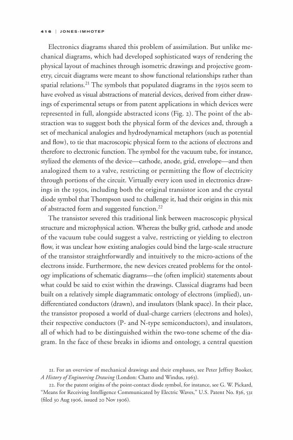
spatial relations.21 The symbols that populated diagrams in the 1950s seem to
have evolved as visual abstractions of material devices, derived from either draw-
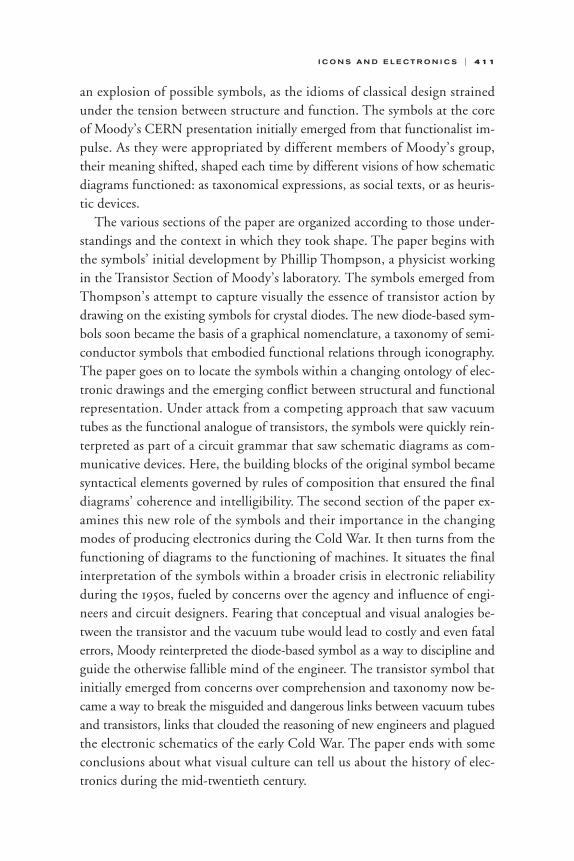
ings of experimental setups or from patent applications in which devices were
represented in full, alongside abstracted icons (Fig. 2). The point of the ab-
straction was to suggest both the physical form of the devices and, through a
set of mechanical analogies and hydrodynamical metaphors (such as potential
and flow), to tie that macroscopic physical form to the actions of electrons and
therefore to electronic function. The symbol for the vacuum tube, for instance,
stylized the elements of the device—cathode, anode, grid, envelope—and then
analogized them to a valve, restricting or permitting the flow of electricity
through portions of the circuit. Virtually every icon used in electronics draw-
ings in the 1950s, including both the original transistor icon and the crystal
diode symbol that Thompson used to challenge it, had their origins in this mix
of abstracted form and suggested function.22
The transistor severed this traditional link between macroscopic physical
structure and microphysical action. Whereas the bulky grid, cathode and anode
of the vacuum tube could suggest a valve, restricting or yielding to electron
flow, it was unclear how existing analogies could bind the large-scale structure
of the transistor straightforwardly and intuitively to the micro-actions of the
electrons inside. Furthermore, the new devices created problems for the ontol-
ogy implications of schematic diagrams—the (often implicit) statements about
what could be said to exist within the drawings. Classical diagrams had been
built on a relatively simple diagrammatic ontology of electrons (implied), un-
differentiated conductors (drawn), and insulators (blank space). In their place,
the transistor proposed a world of dual-charge carriers (electrons and holes),
their respective conductors (P- and N-type semiconductors), and insulators,
all of which had to be distinguished within the two-tone scheme of the dia-
gram. In the face of these breaks in idioms and ontology, a central question
21. For an overview of mechanical drawings and their emphases, see Peter Jeffrey Booker,
A History of Engineering Drawing (London: Chatto and Windus, 1963).
22. For the patent origins of the point-contact diode symbol, for instance, see G. W. Pickard,
“Means for Receiving Intelligence Communicated by Electric Waves,” U.S. Patent No. 836, 531
(filed 30 Aug 1906, issued 20 Nov 1906).
HSNS3803_03 7/10/08 5:58 PM Page 416

I C O N S A N D E L E C T R O N I C S | 4 1 7
emerged: what essential qualities should symbols embody, and how might they
be drawn?
The question was particularly vexing when applied to junction transistors.
The existing Bell symbol had been a schematized drawing of the original ex-
perimental setup built by John Bardeen and Walter Brattain at Bell Labs in
FIG. 2 Patent drawings for de Forest’s vacuum tube (top) and Bardeen and Brattain’spoint-contact transistor (bottom). Circuit symbols emerged as schematized versions of ex-perimental diagrams or patent drawings like these. Note the similarity between the figureat bottom left in the transistor patent and the traditional transistor symbol in Fig. 1. Notealso the use of existing circuit symbols, like capacitors and resistors, alongside the lessabstract drawings of the new devices. Source: Lee de Forest, U.S. Patent 0,879,532; JohnBardeen and Walter Brattain, U.S. Patent 2,524,035. Courtesy of the United States Patentand Trademark Office.
HSNS3803_03 7/10/08 5:58 PM Page 417

4 1 8 | J O N E S - I M H OT E P
1947 for the point-contact transistor. Although the junction transistor had
originally used the same icon, many observers believed it had been orphaned
by the Bell symbol, which spoke to neither its form nor its functioning. At-
tempting to capture the details of the new transistor graphically, proposals
for a new symbol split along two principal lines. One approach embraced the
new ontology by emphasizing material composition and physical form; the
other rejected questions of form in favor of symbols that primarily suggested
function.
Much of the resulting debate was intensely local, taking place in labora-
tory offices and seminar rooms, or within the hermetic Symbols Committee
of the Institute of Radio Engineers (IRE), predecessor of today’s IEEE (In-
stitute of Electrical and Electronics Engineers). When the IRE Symbols Com-
mittee issued its standards for electronic symbols in 1950, for instance, it was
strangely mute on how transistors and semiconductor devices ought to be
drawn. But in July 1952, possibly as a reaction to the growing profusion of
transistor symbols, the committee’s former chair, Allen Pomeroy (himself a
member of the technical staff at Bell Labs), revealed some of its anxieties,
pleading for a single “symbol language” in place of what he saw as the emerg-
ing dystopia of organization-specific symbols that distinguished schematics
at Bell Labs, for instance, from those at RCA.23 When the IRE finally adopted
the Bell symbol in 1957, the compromise language of the Committee reflected
the wider debates. In a remarkable and unusual foreword, the Committee set
out the criteria for its choices: that symbols should “reflect the past,” “look to
the future,” and “indicate physical properties . . . without overcomplication.”24
In the years leading up to that decision, however, the symbols debate went
public as rival symbols sprang up in conference presentations, blackboard
lectures and trade publications. In those challenges the inadequacies of the
Bell symbol stood out, even among those who agreed with the emphasis on
structure and form.
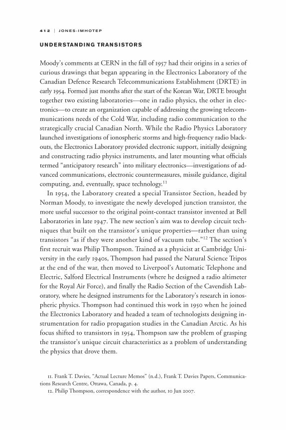
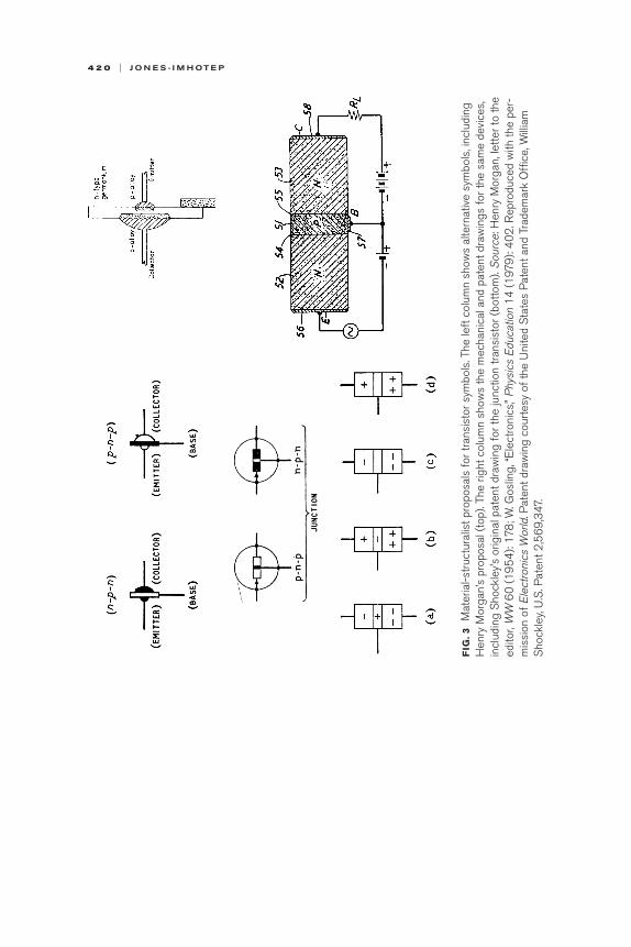
One such challenge appeared in April 1954, when Henry Morgan submit-
ted a one-paragraph note, along with a proposed transistor symbol, to the
journal Wireless World. The standard Bell symbol, Morgan claimed, was fine
in its original context, “but let us have a new symbol for junction transistors,
23. Allen F. Pomeroy, “Universal Engineering Shorthand,” Proceedings of the IRE 40 (1952): 771.
24. IRE Standards on Graphical Symbols for Semiconductor Devices,” Proceedings of the IRE45 (1957): 1612–17, on 1612 (emphasis added).
HSNS3803_03 7/10/08 5:58 PM Page 418
I C O N S A N D E L E C T R O N I C S | 4 1 9
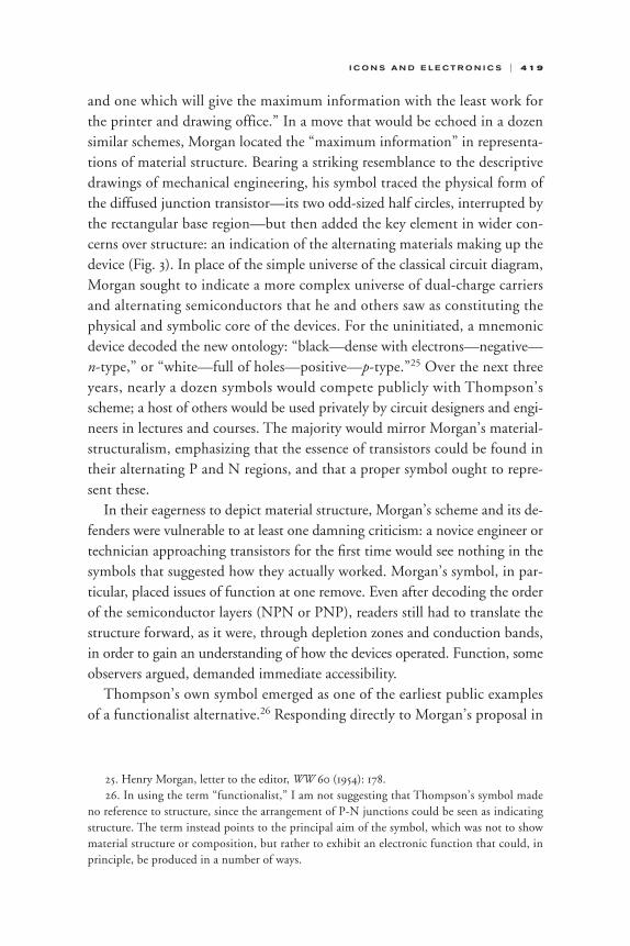
and one which will give the maximum information with the least work for
the printer and drawing office.” In a move that would be echoed in a dozen
similar schemes, Morgan located the “maximum information” in representa-
tions of material structure. Bearing a striking resemblance to the descriptive
drawings of mechanical engineering, his symbol traced the physical form of
the diffused junction transistor—its two odd-sized half circles, interrupted by
the rectangular base region—but then added the key element in wider con-
cerns over structure: an indication of the alternating materials making up the
device (Fig. 3). In place of the simple universe of the classical circuit diagram,
Morgan sought to indicate a more complex universe of dual-charge carriers
and alternating semiconductors that he and others saw as constituting the
physical and symbolic core of the devices. For the uninitiated, a mnemonic
device decoded the new ontology: “black—dense with electrons—negative—
n-type,” or “white—full of holes—positive—p-type.”25 Over the next three
years, nearly a dozen symbols would compete publicly with Thompson’s
scheme; a host of others would be used privately by circuit designers and engi-
neers in lectures and courses. The majority would mirror Morgan’s material-
structuralism, emphasizing that the essence of transistors could be found in
their alternating P and N regions, and that a proper symbol ought to repre-
sent these.
In their eagerness to depict material structure, Morgan’s scheme and its de-
fenders were vulnerable to at least one damning criticism: a novice engineer or
technician approaching transistors for the first time would see nothing in the
symbols that suggested how they actually worked. Morgan’s symbol, in par-
ticular, placed issues of function at one remove. Even after decoding the order
of the semiconductor layers (NPN or PNP), readers still had to translate the
structure forward, as it were, through depletion zones and conduction bands,
in order to gain an understanding of how the devices operated. Function, some
observers argued, demanded immediate accessibility.
Thompson’s own symbol emerged as one of the earliest public examples
of a functionalist alternative.26 Responding directly to Morgan’s proposal in
25. Henry Morgan, letter to the editor, WW 60 (1954): 178.
26. In using the term “functionalist,” I am not suggesting that Thompson’s symbol made
no reference to structure, since the arrangement of P-N junctions could be seen as indicating
structure. The term instead points to the principal aim of the symbol, which was not to show
material structure or composition, but rather to exhibit an electronic function that could, in
principle, be produced in a number of ways.
HSNS3803_03 7/10/08 5:58 PM Page 419
4 2 0 | J O N E S - I M H OT E P
FIG
.3M
ater
ial-s
truc
tura
list p
ropo
sals
for
tran
sist
or s
ymbo
ls. T
he le
ft c
olum
n sh
ows
alte
rnat
ive
sym
bols
, inc
ludi
ngH
enry
Mor
gan’
s pr
opos
al (
top)
. The
rig
ht c
olum
n sh
ows
the
mec
hani
cal a
nd p
aten
t dra
win
gs f
or th
e sa
me
devi
ces,
incl
udin
g S
hock
ley’
s or
igin
al p
aten
t dra
win
g fo
r th
e ju
nctio
n tr
ansi
stor
(bo
ttom
). S
ourc
e: H
enry
Mor
gan,
lett
er to
the
edito
r, W
W6
0 (
19
54
): 1
78; W
. Gos
ling,
“Ele
ctro
nics
,” P
hysi
cs E
duca
tion
14
(1
979
): 4
02
. Rep
rodu
ced
with
the
per-
mis
sion
of
Ele
ctro
nics
Wor
ld.P
aten
t dra
win
g co
urte
sy o
f th
e U
nite
d S
tate
s P
aten
t and
Tra
dem
ark
Offi
ce, W
illia
mS
hock
ley,
U.S
. Pat
ent 2
,56
9,3
47.
HSNS3803_03 7/10/08 5:58 PM Page 420

I C O N S A N D E L E C T R O N I C S | 4 2 1
June 1954, Thompson submitted his own diode-based symbol to WirelessWorld. His main criticism targeted Morgan’s “excessive concern with me-
chanical form.” Juxtaposing his own symbol against Morgan’s, Thompson
explained, “You will note that our convention has been developed from the
electrical function of transistors rather than their mechanical form.”27 But
Thompson’s scheme itself rested on a particular understanding of what “func-
tion” meant. In the details of his scheme, he had located “electrical function”
in circumscribed questions about mechanism. Here, the rectifying junction
acted as the key functional unit, the black box. Put differently, what mat-
tered for Thompson was not so much what transistors were made of or how
their materials were arranged, but rather that their operations were based on
a rectifying action that might, in principle, be achieved in a number of ways.
The diode symbol was then introduced to symbolize the junction and shift
the workings of the transistors onto familiar visual and conceptual grounds.
In endorsing Thompson’s symbol, the editors of Wireless World called this
the “historical” approach, since “the user is going from the known to the un-
known.”28
But there were other possible “histories.” One particularly compelling one
rested on a wholly different understanding of what it meant to demonstrate
“function.” It involved stepping further back, shedding the quantum physics
of electrons and semiconductors altogether, and even the operationalized pic-
ture of junctions, to see the entire device as the black box. Jerome Kurshan,
for instance, one of RCA Laboratories’ first transistor researchers and head
of the Tubeless Amplifier group, initially approached the transistor by shelv-
ing solid-state theory, focusing instead on measurements of input, output,
and ratio of amplification. He would ultimately define the transistor func-
tionally, as a device that amplified electric current without vacuum tubes.29
Under Kurshan and others, function became a question, not of mecha-
nism, but of behavior. The key question—how did transistors work?—
was really another question: what work did transistors do? How did they op-
erate within the context of circuits and electrical variations? As Kurshan’s
operationalization suggested, one dominant answer pointed away from recti-
fiers and solid-state electronics altogether, and toward the larger category of
27. Philip M. Thompson, “Transistor Symbols,” WW 60 (1954): 325 (emphasis added).
28. Editorial, “Transistor Symbols,” WW 61 (1955): 151.
29. Choi, “Boundaries of Industrial Research” (ref. 3), 763.
HSNS3803_03 7/10/08 5:58 PM Page 421

4 2 2 | J O N E S - I M H OT E P
three-contact devices known as “triodes.” Viewed in this way, with the tran-
sistor itself as monolith, the natural analogies were no longer with semicon-
ductor diodes, as Thompson argued, but with the triodes that dominated the
material and design cultures of electronics in the mid-twentieth century—
vacuum tubes.30 Functionalism relied on emphasizing function through vi-
sual analogies with existing electronic parts; but exactly which devices served
as the proper referent hinged on one’s view of the meaning of “function.”
The debate over electronic representation was an occasion for disagreements
over what transistors really were—semiconducting analogues of the vacuum
tube or evolved solid-state diodes. Because functional symbols argued for how
transistors worked, and therefore shaped understandings of how they should
figure in questions of design, the stakes over how to show function were enor-
mous. It is on this debate among the proponents of functional representation,
and particularly their disagreements over the links to vacuum tubes, that the
rest of this paper focuses.
U N D E R STAN D I NG TRAN S I STOR S I I
The view that the transistor represented an analogue of the vacuum tube had
begun with its inventors. In 1936, Bell Laboratories’ Director of Research, Mervin
Kelly, launched the search to replace the electromechanical relays that he believed
formed a bottleneck for Bell’s expanding telephonic empire. Vacuum tubes, which,
like all amplifiers, could also be used as switches, were too bulky, power-hungry,
and unreliable. So Kelly, a former director of vacuum tube development, sug-
gested semiconductor amplifiers might furnish the ideal alternative.31 From its
inception, the research program that produced the transistor aimed to produce
a solid-state version of the vacuum tube.32 That understanding drove the image
30. Indeed, because of the analogy with the vacuum tube, the staff of Bell Labs considered a
number of possible names—“semiconductor triode,” “surface states triode,” “crystal triode”—
before agreeing on “transistor.” See John R. Pierce, “The Naming of the Transistor,” Proceedingsof the IEEE 86 (1998): 37–45.
31. Jack Morton, Organizing for Innovation: A Systems Approach to Technical Management (New
York: McGraw-Hill, 1971), 46–48.
32. That understanding was so strong, in fact, that William Shockley initially tried to place a
copper grid inside a semiconductor crystal. See Riordan and Hoddeson, “Electron” (ref. 3), 5;
Gerald L. Pearson and William H. Brattain, “History of Semiconductor Research,” Proceedings
HSNS3803_03 7/10/08 5:58 PM Page 422

I C O N S A N D E L E C T R O N I C S | 4 2 3
of the device after its invention. In their first published description, entitled “The
Transistor, A Semiconductor Triode,” Bardeen and Brattain described their in-
vention as a “three-element electronic device,” a triode that could be employed
“as an amplifier, oscillator, and for any other purposes for which vacuum tubes areordinarily used.”33 Bell’s publicity campaign quickly reinforced the view. In 1948,
it demonstrated to its own staff a radio whose vacuum tubes had been entirely
replaced by transistors. That summer, the New York Times reported on the new
device, “called a transistor, which has several applications in radio where a vac-
uum tube ordinarily is employed.”34 Symbolic connections soon spilled onto
the shop floor as manufacturers like Westinghouse, RCA, and Bell placed the
production and development of transistors in their tube divisions.35 Writing in
Scientific American, Louis Ridenour gave the substitution moral force, suggest-
ing that there was nothing wrong with electronics that the elimination of the vac-
uum tube could not fix.36
In early 1957, those connections made their way into the debate over tran-
sistor symbols. They were most prominent in the writing of Marcus Scroggie,
a former radar instructor with the British Royal Air Force, whose textbook,
Foundations of Wireless, would become a classic. Born in Scotland and trained
at the University of Edinburgh, Scroggie worked for various radio and elec-
tronics companies in the 1930s before serving as a radar operator for the RAF.
He eventually became an instructor at the RAF Radar School, where the Air
Ministry put him in charge of its secret publications on radio and radar. In the
early 1950s he was best known for his regular columns in Wireless World, writ-
ten under the pseudonym “Cathode Ray.”
Starting in July 1956, Scroggie published a series of brilliant articles intro-
ducing readers to semiconductors and transistors. He began by noting that
transistors generally received one of two opposing treatments in the literature.
Some authors, claiming that one could use transistors without knowing how
of the IRE 43 (1955): 1794–806; Walter Brattain, “Genesis of the Transistor,” Physics Teacher 6,
no. 3 (1968): 109–14. For a general account of this view of the transistor, see Stuart Macdonald
and Ernest Braun, “The Transistor and Attitude Towards Change,” American Journal of Physics45, no. 11 (1977): 1062–63.
33. J. Bardeen and W. H. Brattain, “The Transistor, A Semiconductor Triode,” Physical Review74 (1948): 230–31, on 230.
34. “The News of Radio,” New York Times, 1 Jul 1948.
35. See, for example, Leslie, “Blue Collar Science” (ref. 3), 89–90.
36. Louis N. Ridenour, “A Revolution in Electronics,” Scientific American 185 (1951): 13–17.
HSNS3803_03 7/10/08 5:58 PM Page 423
4 2 4 | J O N E S - I M H OT E P
they worked, portrayed the devices through their “black box” representations
as current-source-equivalent circuits. Others, seizing on the detailed physics
behind transistor action, launched into Fermi-Dirac statistics, wave mechan-
ics, and “all that” to explain the actions of electrons in solids. Unimpressed in
equal measure by pragmatic operationalism and high-flown theory, Scroggie
ventured a guess about his readers: “I suspect there are a large number of peo-
ple who would like a simple picture of what goes on in transistors, to hang up
in their minds alongside the picture they already have of what goes on in valves—
the nice clear picture of electrons boiling off from the hot cathode and stream-
ing across to the attractive anode, to an extent controlled by raising or lower-
ing the potential of an intervening grid.”37 This gesture towards understanding
transistors as the counterpart of vacuum tubes would inform Scroggie’s criti-
cism of Thompson’s scheme and shape his vision of an appropriate icon.
In launching into transistors, Scroggie realized that the “nice clear picture”
he was after lay obscured in the confusing details of electron behavior in solids.
He went on to negotiate a careful middle ground for his readers: “One thing
we shall see is that the complicated picture of some of the actions [in transis-
tors] can be replaced for routine purposes by a more condensed description,
the details being, as it were, ‘understood.’” As if presaging a confrontation
with Thompson, Scroggie added, “I only hope that the necessary simplifica-
tions will not make the physicists squirm too much.” With this, Scroggie began
a discussion of electrical currents in solids. Vacuum tubes, he explained, were
so easy to understand because the electrons released from the cathode traveled
through a near vacuum rather than the “jungle” of fixed atoms that made up
semiconductors, whose detailed behavior depended on advanced chemistry
and physics.38 Avoiding that advanced discussion altogether, Scroggie moved
on to the structure of atoms and explanations of shared electrons (both ther-
mally and photo-electrically released), intrinsic conductivity, P- and N-type
doping, and finally P-N junctions. Noting the tendency of junctions to priv-
ilege current flow in one direction and summarizing his material so far, he
concluded (just as Thompson had two years before), “In brief, a P-N junction
is a rectifier.”39
37. Marcus Scroggie [Cathode Ray, pseud.], “Semi-conductors—1,” WW 62 (1956): 317–21,
on 317.
38. Ibid., 317–18.
39. Marcus Scroggie [Cathode Ray, pseud.], “Semi-conductors—2: Another Step on the Way
to Transistors,” WW 62 (1956): 394–98, on 397.
HSNS3803_03 7/10/08 5:58 PM Page 424

I C O N S A N D E L E C T R O N I C S | 4 2 5
Here the two approaches diverged. Thompson had used the insight about
P-N junctions to link transistors to solid-state diodes and to the wider world
of semiconductor devices. Scroggie’s connections cut orthogonally. In the last
of his expository essays, published in August 1956, Scroggie sought to link the
transistor not to semiconductor diodes—the solid-state rectifiers that composed
transistors in the form of P-N junctions—but rather to vacuum tubes. Begin-
ning with a caution, Scroggie explained that in order to obtain “a transfer ticket
from valves to transistors,” one had to recognize certain key differences: that
vacuum tubes emitted only electrons from their cathode, whereas transistors
employed both electrons and holes; or that electrons emitted from a valve’s
cathode moved through a vacuum, whereas electrons in transistors made their
way through a germanium or silicon crystal lattice.40 But the caution only un-
derlined Scroggie’s principal aim of presenting the transistor as a functional
analogue of the valve. Thompson had grouped devices according to their junc-
tions, with all their untidy physics; Scroggie grouped them according to oper-
ational homologies. Viewed en bloc, all diodes functioned the same way, priv-
ileging current flow in a single direction, regardless of specific make-up.
Triodes—three-contact devices, such as vacuum tubes or transistors—might
differ in their details, but not in their basic electronic operation and structure.
In a series of examples, Scroggie explicitly and visually translated semiconduc-
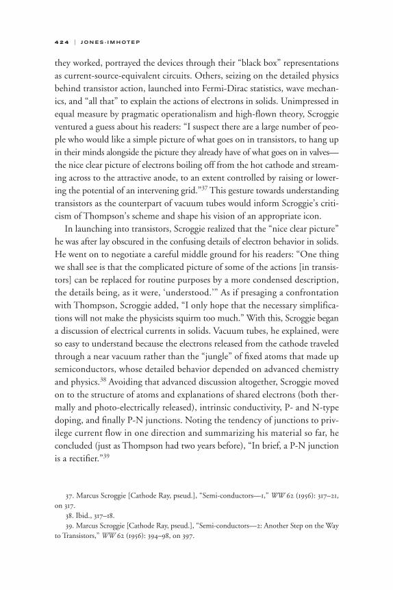
tor behavior and circuits into their vacuum-tube equivalents (Fig. 4). Current
flow in diodes moved from disembodied charges to the interchangeable forms
of vacuum tubes and their crystal analogues; a discussion of basic transistor
arrangements erected solid-state circuits on a foundation of thermionic coun-
terparts. Again and again throughout his insightful discussion, Scroggie drew
his lines of relation, his “histories,” visually from transistors to valves and back
again. To judge from the drawings, nothing functioned so much like a tran-
sistor as did a vacuum tube.
Drawing Connections
In April 1957, his introduction to transistors complete, Scroggie used his col-
umn in Wireless World as an opportunity to wade into the debate over symbols.
Surveying most of the proposals that had come into the journal, Scroggie
observed that with the exception of Thompson’s, all used the original Bell
40. Marcus Scroggie [Cathode Ray, pseud.], “Transistors: An Introduction for Beginners,”
WW 62 (1956): 449–53, on 449.
HSNS3803_03 7/10/08 5:58 PM Page 425
4 2 6 | J O N E S - I M H OT E P
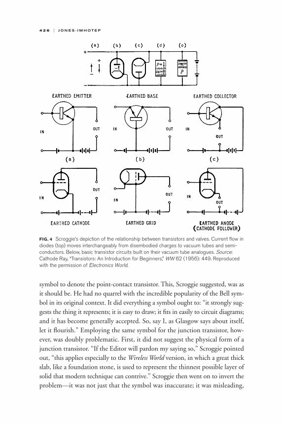
symbol to denote the point-contact transistor. This, Scroggie suggested, was as
it should be. He had no quarrel with the incredible popularity of the Bell sym-
bol in its original context. It did everything a symbol ought to: “it strongly sug-
gests the thing it represents; it is easy to draw; it fits in easily to circuit diagrams;
and it has become generally accepted. So, say I, as Glasgow says about itself,
let it flourish.” Employing the same symbol for the junction transistor, how-
ever, was doubly problematic. First, it did not suggest the physical form of a
junction transistor. “If the Editor will pardon my saying so,” Scroggie pointed
out, “this applies especially to the Wireless World version, in which a great thick
slab, like a foundation stone, is used to represent the thinnest possible layer of
solid that modern technique can contrive.” Scroggie then went on to invert the
problem—it was not just that the symbol was inaccurate; it was misleading,
FIG. 4 Scroggie’s depiction of the relationship between transistors and valves. Current flow indiodes (top) moves interchangeably from disembodied charges to vacuum tubes and semi-conductors. Below, basic transistor circuits built on their vacuum tube analogues. Source:Cathode Ray, “Transistors: An Introduction for Beginners,” WW 62 (1956): 449. Reproducedwith the permission of Electronics World.
HSNS3803_03 7/10/08 5:58 PM Page 426

I C O N S A N D E L E C T R O N I C S | 4 2 7
since it suggested that junction transistors were point-contact devices. “So,
looking at a transistor circuit diagram, one wastes time searching for informa-
tion on which kind of transistor is meant. If point-contacts become completely
obsolete that objection will disappear, but we will still be left with an absurdly
inappropriate symbol.”
One by one, Scroggie dispatched the competing symbols through a series of
criteria that any good representation should meet: it should “suggest” a junc-
tion transistor (presumably through a reference to form); it should be easy to
draw on paper or blackboard; and it should be easy to distinguish from all other
symbols. Symbols that required shading of some sort violated ease of drawing,
and had to go. “Life these days is just too short,” Scroggie quipped. A remain-
ing symbol belonging to E. Aisberg, editor of Toute la radio, showed the emit-
ter and collector on the same side, a violation of the demand that a represen-
tation suggest physical form. “So all go.”41
Instead, Scroggie turned to one of the most popular early textbooks on the
subject. Transistor Electronics had been co-written by five members of RCA who
had developed their own transistor symbol (Fig. 5). Scroggie had already been
using the symbol for some time, privately and in his teachings. He liked that
it emphasized the thinness of the base and that it put collector and emitter on
opposite sides. “Accepted practice rightly favors circuit symbols that primarily
41. Marcus Scroggie [Cathode Ray, pseud.], “Transistor Graphic Symbols: A Critical Analy-
sis of Existing Ideas and Conventions,” WW 63 (1957): 194–98, on 194–95.
FIG. 5 The RCA symbol. The arrow at the bottom represents the emitter,the center line is the base, and the T-shaped portion at the top is the col-lector. Note the similarities with the common vacuum tube symbol, shownon the right, from which the enclosing circle is borrowed. Source: CathodeRay, “Transistor Graphic Symbols: A Critical Analysis of Existing Ideas andConventions,” WW 63 (1957): 194–98. Reprinted with the permission ofElectronics World. Vacuum tube symbol reprinted with permission fromIEEE Standard 54 IRE 21 S1, IRE Standards on Graphical Symbols,Copyright 1954, by IEEE.
HSNS3803_03 7/10/08 5:58 PM Page 427
4 2 8 | J O N E S - I M H OT E P
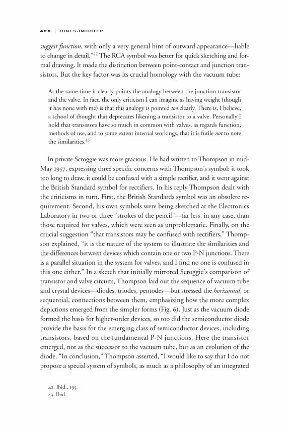
suggest function, with only a very general hint of outward appearance—liable
to change in detail.”42 The RCA symbol was better for quick sketching and for-
mal drawing. It made the distinction between point-contact and junction tran-
sistors. But the key factor was its crucial homology with the vacuum tube:
At the same time it clearly points the analogy between the junction transistor
and the valve. In fact, the only criticism I can imagine as having weight (though
it has none with me) is that this analogy is pointed too clearly. There is, I believe,
a school of thought that deprecates likening a transistor to a valve. Personally I
hold that transistors have so much in common with valves, as regards function,
methods of use, and to some extent internal workings, that it is futile not to note
the similarities.43
In private Scroggie was more gracious. He had written to Thompson in mid-
May 1957, expressing three specific concerns with Thompson’s symbol: it took
too long to draw, it could be confused with a simple rectifier, and it went against
the British Standard symbol for rectifiers. In his reply Thompson dealt with
the criticisms in turn. First, the British Standards symbol was an obsolete re-
quirement. Second, his own symbols were being sketched at the Electronics
Laboratory in two or three “strokes of the pencil”—far less, in any case, than
those required for valves, which were seen as unproblematic. Finally, on the
crucial suggestion “that transistors may be confused with rectifiers,” Thomp-
son explained, “it is the nature of the system to illustrate the similarities and
the differences between devices which contain one or two P-N junctions. There
is a parallel situation in the system for valves, and I find no one is confused in
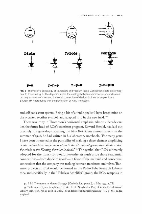
this one either.” In a sketch that initially mirrored Scroggie’s comparison of
transistor and valve circuits, Thompson laid out the sequence of vacuum tube
and crystal devices—diodes, triodes, pentodes—but stressed the horizontal, or
sequential, connections between them, emphasizing how the more complex
depictions emerged from the simpler forms (Fig. 6). Just as the vacuum diode
formed the basis for higher-order devices, so too did the semiconductor diode
provide the basis for the emerging class of semiconductor devices, including
transistors, based on the fundamental P-N junctions. Here the transistor
emerged, not as the successor to the vacuum tube, but as an evolution of the
diode. “In conclusion,” Thompson asserted, “I would like to say that I do not
propose a special system of symbols, as much as a philosophy of an integrated
42. Ibid., 195.
43. Ibid.
HSNS3803_03 7/10/08 5:58 PM Page 428
I C O N S A N D E L E C T R O N I C S | 4 2 9
and self consistent system. Being a bit of a traditionalist I have based mine on
the accepted rectifier symbol, and adapted it to fit the new field.”44
There was irony in Thompson’s horizontal emphasis. Almost a decade ear-
lier, the future head of RCA’s transistor program, Edward Herold, had laid out
precisely this genealogy. Reading the New York Times announcement in the
summer of 1948, he had written in his laboratory notebook, “For many years
I have been interested in the possibility of making a three-element amplifying
crystal which bears the same relation to the silicon and germanium diode as doesthe triode to the Fleming thermionic diode.”45 The symbol that RCA ultimately
adopted for the transistor would nevertheless push aside those sequential
connections—from diode to triode—in favor of the material and conceptual
connections that the company was making between transistors and valves. Tran-
sistor projects at RCA would be housed in the Radio Tube Research Labora-
tory, and specifically in the “Tubeless Amplifier” group; the RCA symposia in
44. P. M. Thompson to Marcus Scroggie [Cathode Ray, pseud.], 31 May 1957, 2, TP.
45. “Solid-state Crystal Amplifiers,” E. W. Herold Notebooks, P–2758, in the David Sarnoff
Library, Princeton, NJ, as cited in Choi, “Boundaries of Industrial Research” (ref. 3), 761, added
emphasis.
FIG. 6 Thompson’s genealogy of transistors and vacuum tubes. Connections here are orthog-onal to those in Fig. 4. The depiction notes the analogy between semiconductors and valves,but only as a way of stressing the serial connection of devices to their to simpler forms.Source: TP. Reproduced with the permission of P. M. Thompson.
HSNS3803_03 7/10/08 5:58 PM Page 429
4 3 0 | J O N E S - I M H OT E P
1952, which presented transistors and their applications to possible clients, drew
direct analogies between the emerging junction transistor and the vacuum tube.
Ultimately, the symbol developed by the largest tube manufacturer in the United
States would reinforce those connections, rather than the genealogy elaborated
in Herold’s notebook or Thompson’s iconography.46 The two symbols, RCA’s
and Thompson’s, would eventually confront each other directly in September
1957; but not before their meanings had shifted away from concerns about
essence and isolated, individual acts of comprehension to anxieties about the
wider social world that drawings inhabited and the mediating role of symbols
within it.
CI RCU IT SYNTAX AN D TH E R E LIAB LE D IAG RAM
The disagreements over transistor symbols were ultimately possible because of
an initial consensus about schematic diagrams—the larger depictions of cir-
cuits that individual symbols populated. For all their differences about how to
draw transistors, Thompson and Scroggie both saw schematics as extensions
of the mental apparatus of the engineer. Standing between thought and arti-
fact, they were the sites where machines were first speculatively assembled, op-
erated, taken apart, and reconfigured. It was because of the way schematics
helped engineers to think through the work of designing electronics that sym-
bols had to capture the defining qualities of devices. In December 1948 Scroggie
had argued for one view of schematics by focusing on a critical feature: their
heuristic power for designers and engineers at work. Likening them to the sys-
tem of Arabic numerals, Scroggie called them “a practically indispensable aid
to thought; simple and effective.” He summoned the image of circuit design-
ers leaning intently over drawings, rather than material circuits, when a piece
of circuitry behaved unexpectedly. In fact, Scroggie pressed on, schematics were
so effective that they created “the danger of handing over to them too much
of our reasoning powers,” possibly fooling designers into believing that what-
ever existed in the diagram represented the totality of what happened in the
circuit.47 The British physicist L. H. Bainbridge-Bell echoed Scroggie’s em-
phasis on circuit diagrams as specialized thought-tools. They should not be
46. “Tentative Presentations for Licensee Transistor Meetings, October 30, 1952,” 1, as cited
in Choi, “Boundaries of Industrial Research” (ref. 3), 771.
47. Marcus Scroggie [Cathode Ray, pseud.], “Invisible Components: What the Circuit Dia-
gram Fails to Show,” WW 54 (1948): 459–62, on 459.
HSNS3803_03 7/10/08 5:58 PM Page 430

I C O N S A N D E L E C T R O N I C S | 4 3 1
confused or combined with layout drawings, for instance, which gave exact
spatial relations, useful for a purpose entirely different.48 In the hands of Scrog-
gie and Bainbridge-Bell, the circuit diagram was a crucial “paper tool,” used to
think through the workings of material artifacts before they took physical form
and after things went awry.49
Another view, however, saw schematics not so much as the thought-things
of individual engineers and designers, but as public artifacts meant to com-
municate and coordinate among the various groups implicated in the con-
struction of artifacts. Throughout the spring of 1957, that debate over symbols
had been characterized by an anxiety about the individual engineer, struggling
(like Thompson had) to make sense of transistors. Over the summer of 1957,
however, the focus of the discussion shifted from the heuristic value of sym-
bols to their communicative function. The key figure in that transformation
was a former British RAF signals officer and senior research technician at the
Radio Physics Laboratory named Jack Bateson. Throughout his years at RPL,
Bateson distinguished himself not only through his remarkable skills as a tech-
nician and teacher, but also through his commitment to pedagogy, especially
clear and proper exposition. At yearly symposia Bateson would make careful,
often exhaustive, stylistic commentaries on his colleagues’ technical lectures—
how they handled slides and overhead transparencies, the cadence of their
speech, their use of grammar, and their expository style.50
Circuit diagrams intersected Bateson’s concerns about language through at
least two points. One was syntax: like the constructions of natural language,
circuit diagrams were compositions, built up from more fundamental symbols
(resistors, capacitors, vacuum tubes, inductors, transformers, and so on).51 Just
as the rules of syntax shaped proper expression in natural language, so the rules
48. L. H. Bainbridge-Bell, “Circuit Symbols: Notes on the New British Standard,” WW 54
(1948): 437–38, on 437.
49. Here I borrow the term “paper tool” from Ursula Klein and David Kaiser. See Ursula
Klein, “Techniques of Modeling and Paper-tools in Classical Chemistry,” in Models as Mediators:Perspectives on Natural and Social Science, ed. Mary Morgan and Margaret Morrison (New York:
Cambridge University Press, 1999), 146–67; Ursula Klein, “Paper Tools in Experimental Cul-
tures,” Studies in the History and Philosophy of Science 32 (2001): 265–302; Ursula Klein, Experi-ments, Models and Paper Tools: Cultures of Organic Chemistry in the Nineteenth Century (Palo Alto,
CA: Stanford University Press, 2003); and David Kaiser, Drawing Theories Apart (ref. 8), chap. 1.
50. J. Bateson, “The Defence Research Board fifth symposium,” 3 Dec 1953, 2, TP.
51. Bateson’s views unconsciously built on a long and fascinating history of technical artifacts
as language systems. The eighteenth-century Swedish technologist Christopher Polhem con-
structed a “mechanical alphabet” in which the “five powers”—levers, wedges, screws, pulleys, and
HSNS3803_03 7/10/08 5:58 PM Page 431

4 3 2 | J O N E S - I M H OT E P
of electronic design governed the proper graphical articulation of circuits. The
placement of power supplies, the direction of signal travel, and graphic con-
ventions for crossing wires were more than simple matters of etiquette for Bate-
son; they were what made circuits clear and meaningful, structuring how draw-
ings should be read and understood. Here diagrams provided a second point
of intersection with concerns about language. Whether appearing in engineering
journals or spread across the workbench, circuit diagrams were instruments of
effective communication; they were directed toward an audience. In Bateson’s
own Radio Physics Laboratory, a set of drawings might move from engineer to
technician and back a dozen times, with individual circuits and elements con-
tributed by just as many people. Breakdowns of communication through dia-
grams jeopardized the effectiveness of radars and communication circuits. As
Bateson’s colleague Philip Thompson would later explain, “circuits will be con-
tributed by a variety of individuals, and they will be compatible only if there
is some central guidance in a few fundamentals.”52 Rules of composition en-
sured compatibility in this production system.
Bateson soon brought these concerns over syntax and communication to
bear on the debate over symbols. He had eagerly followed the discussion of
transistor symbols in Wireless World. Philip Thompson was a colleague at RPL’s
sibling, the Electronics Laboratory, and Bateson had long followed Marcus
Scroggie’s columns, where he admired Scroggie’s expository abilities, particu-
larly the “ruthless scorn” to which Scroggie subjected misguided thinking in
electronics. He had even drawn on Scroggie’s style to make his own colleagues
better “platform expositors.”53 But Scroggie’s discussion of transistor symbols
represented a breach. “I feel bound to protest,” Bateson wrote to Scroggie di-
rectly. “I rather suspect that Mr. P. M. Thompson, with whom I occasionally
establish contact across the 30 miles that separate us by means of another of
Bell’s inventions, will protest also.”54
For Bateson, Scroggie’s criticisms of the diode-based symbol hinged on a
fundamental misunderstanding of what circuit symbols were. Like the larger
schematics to which they belonged, symbols aimed at clear communication.
winches—functioned as the vowels, while the other elements provided the consonants. He sug-
gested that the proper metaphor for technological development was composition, rather than
invention.
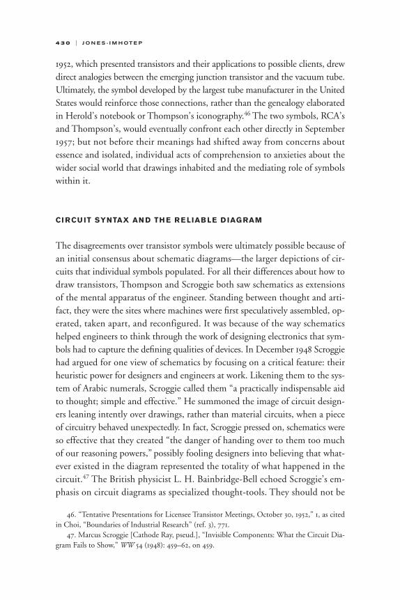
52. Philip Thompson to Seymour Schwartz, 1 Aug 1958, TP.
53. Jack Bateson to Marcus Scroggie [Cathode Ray, pseud.], 15 Apr 1957, TP.
54. Ibid.
HSNS3803_03 7/10/08 5:58 PM Page 432
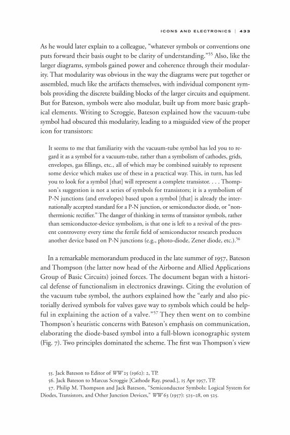
I C O N S A N D E L E C T R O N I C S | 4 3 3
As he would later explain to a colleague, “whatever symbols or conventions one
puts forward their basis ought to be clarity of understanding.”55 Also, like the
larger diagrams, symbols gained power and coherence through their modular-
ity. That modularity was obvious in the way the diagrams were put together or
assembled, much like the artifacts themselves, with individual component sym-
bols providing the discrete building blocks of the larger circuits and equipment.
But for Bateson, symbols were also modular, built up from more basic graph-
ical elements. Writing to Scroggie, Bateson explained how the vacuum-tube
symbol had obscured this modularity, leading to a misguided view of the proper
icon for transistors:
It seems to me that familiarity with the vacuum-tube symbol has led you to re-
gard it as a symbol for a vacuum-tube, rather than a symbolism of cathodes, grids,
envelopes, gas fillings, etc., all of which may be combined suitably to represent
some device which makes use of these in a practical way. This, in turn, has led
you to look for a symbol [that] will represent a complete transistor. . . . Thomp-
son’s suggestion is not a series of symbols for transistors; it is a symbolism of
P-N junctions (and envelopes) based upon a symbol [that] is already the inter-
nationally accepted standard for a P-N junction, or semiconductor diode, or “non-
thermionic rectifier.” The danger of thinking in terms of transistor symbols, rather
than semiconductor-device symbolism, is that one is left to a revival of the pres-
ent controversy every time the fertile field of semiconductor research produces
another device based on P-N junctions (e.g., photo-diode, Zener diode, etc.).56
In a remarkable memorandum produced in the late summer of 1957, Bateson
and Thompson (the latter now head of the Airborne and Allied Applications
Group of Basic Circuits) joined forces. The document began with a histori-
cal defense of functionalism in electronics drawings. Citing the evolution of
the vacuum tube symbol, the authors explained how the “early and also pic-
torially derived symbols for valves gave way to symbols which could be help-
ful in explaining the action of a valve.”57 They then went on to combine
Thompson’s heuristic concerns with Bateson’s emphasis on communication,
elaborating the diode-based symbol into a full-blown iconographic system
(Fig. 7). Two principles dominated the scheme. The first was Thompson’s view
55. Jack Bateson to Editor of WW 25 (1962): 2, TP.
56. Jack Bateson to Marcus Scroggie [Cathode Ray, pseud.], 15 Apr 1957, TP.
57. Philip M. Thompson and Jack Bateson, “Semiconductor Symbols: Logical System for
Diodes, Transistors, and Other Junction Devices,” WW 63 (1957): 525–28, on 525.
HSNS3803_03 7/10/08 5:58 PM Page 433
4 3 4 | J O N E S - I M H OT E P
FIG. 7 The expanded diode-based system. Here Thompson and Bateson elaborated both thesystem for constructing symbols and the rules for incorporating them into circuit diagrams.Source: Philip M. Thompson and Jack Bateson, “Semiconductor Symbols: Logical System forDiodes, Transistors and Other Junction Devices,” WW 63 (1957): 525. Reproduced with thepermission of Electronics World.
HSNS3803_03 7/10/08 5:58 PM Page 434

I C O N S A N D E L E C T R O N I C S | 4 3 5
of a “logical, self-consistent, graphical nomenclature” for semiconductors,
based on the diode symbol, and capable of depicting any device that depended
on P-N junctions. On the genetic link to the diode symbol, the authors were
emphatic: “The connection between junction diodes and junction transistors
was a logical one,” they explained, “and not easily broken, and there was no
real reason for trying to break it.”58 The second key feature was the emphasis
on the ability of the symbols, and the schematics containing them, to com-
municate reliably the intentions of the designer to other engineers and tech-
nicians. “Schematic circuit diagrams are line expositions of circuits,” the
authors explained, in Bateson’s characteristic language. “These line pictures
should be as easy to read as the pictures or descriptive texts that go with them.”59
They continued, “In general, it should be remembered that the contribution
made by the eye when reading a diagram is greater than that made by words.
The appearance of the diagram, therefore, is not unimportant.”60 In place of
the existing patchwork of semiconductor symbols, the authors stressed prin-
ciples and logic, rules, and fundamentals. Together with a set of guidelines—
connections to positive supplies should be upward; connection to negative
supplies should be downward with ground in between; signals should travel
from left to right, and so on—the new system, its authors argued, would re-
duce the drawing and reading of circuits to a set of logical and straightforward
principles.
But even as Thompson’s symbols entered the broader debates over semiotics
and circuit diagrams, their meanings were shifting again. Thompson’s initial
intervention had been motivated by the individual act of comprehension—the
lone engineer unlocking the workings of the transistor through a revelatory
symbol. Through his debate with Scroggie and collaboration with Bateson, the
symbols became instruments directed outward, away from the comprehension
of circuit designers and engineers themselves, and toward communication and
pedagogy. And in the hands of Thompson’s supervisor, Norman Moody, they
would finally turn inward again. No longer mere instruments for communi-
cation, they became a way to discipline the minds of the engineer and the cir-
cuit designer, and to save Cold War electronics from itself.
58. Ibid.
59. Ibid., 4.
60. Ibid.
HSNS3803_03 7/10/08 5:58 PM Page 435
4 3 6 | J O N E S - I M H OT E P
FROM PH I LOSOPHY TO ART:
SYM BOLS AN D TH E R E LIAB LE D E S IG N E R
This last transformation in the meaning of Thompson’s symbols was rooted
in a deep ambivalence about electronics that ran through the 1950s. Writing
on the impact of the transistor in early 1958, Jack Morton at Bell Laboratories
expressed this ambivalence well. Stressing the transistor’s transformative power,
Morton laid out a broad cybernetic vision where electronics extended the
visual, mental, and tactile capacities of “electronic man,” projecting the human
mind even more forcefully than nuclear weapons projected human strength.
Those capacities, however, came at a price. Morton cautioned, “all such func-
tions suffer from what has been called ‘the tyranny of numbers.’”61 The com-
plexity of circuits carrying out those advanced functions required hundreds,
thousands, even tens of thousands of electron devices. And as the number of
circuit components increased, so did the likelihood of circuit failure.62 One
had only to look to the beginning of the decade and the Korean War, when
electronic failures had grounded a squadron of Marine Panther jets only months
before malfunctions in dense fog sent them into a mountainside.63 Electron-
ics would later be partly blamed for the disastrous failure of tactical missions.
Barely two weeks after the armistice, one influential report suggested that Korea
was only the tip of the iceberg: two-thirds of U.S. military equipment was likely
malfunctioning.64 By the time Morton made his comments, concerns had spread
to the sprawling integrated systems of radar, targeting, and guided missiles that
secured continental defense and nuclear deterrence. The threat that electronic
failure posed, not only to limited tactical missions but also to the broader
strategic aims of the Cold War itself, created what contemporaries called the
61. J. A. Morton and W. J. Pietenpol, “The Technological Impact of Transistors,” Proceedingsof the IRE 46 (1958): 955–59, on 955.
62. Morton saw this as an economic effect, in that the cost of making vacuum tubes reliable
had held back the development of advanced electronic systems. The corollary was, of course, that
with existing vacuum tubes, complex electronics were dangerously prone to failure.
63. On the proportion of malfunctioning equipment to functioning equipment, see Keith
Henney, ed., Reliability Factors for Ground Electronic Equipment (New York: McGraw-Hill, 1956),
1–1. For reference to Korea, see Chester Soucy, “Present Unreliability,” briefing to the Depart-
ment of National Defence and Services, 30 Dec 1954, 2, NAC, RG24, vol. 2484, file 801–E447–1,
part 1.
64. R. R. Carhart, “A Survey of the Current Status of the Electronic Reliability Problem,”
U.S. Air Force Project RAND Research Memorandum RM–1131 (Santa Monica, CA: RAND
Corporation, 1953), 66.
HSNS3803_03 7/10/08 5:58 PM Page 436

I C O N S A N D E L E C T R O N I C S | 4 3 7
“reliability crisis,” launching the most wide-ranging and comprehensive ex-
amination of electronic reliability ever mounted.
Morton’s now-classic invocation of the “tyranny of numbers” captured the
deep anxiety about electronic complexity in the late 1950s. On the most com-
mon reading, Morton was merely crystallizing a widespread understanding that
reliability in complex circuits was a problem of interconnections: as systems in-
cluded more and more parts, the fallible solder joints that connected them mul-
tiplied, generating site after site of potentially imminent failure. In this way, he
was simply articulating the famous “interconnection problem,” which the in-
tegrated circuit would ultimately solve.65
But that interpretation of Morton’s comments collapses the complexity of
the reliability problem into a prehistory of the integrated circuit, a misreading
that obscures Morton’s real concerns. Closer attention to Morton’s comments
in the spring of 1958 suggests that they were not at all about interconnections.
For him, the “tyranny of numbers” expressed a problem of electronic parts,specifically vacuum tubes, not their interconnections. As complex systems in-
corporated more and more tubes, reliability plummeted. The power-hungry
and inherently unreliable vacuum tubes therefore placed limits on circuit com-
plexity, stifling the enormous potential of electronics to extend human capa-
bilities. Tubes could be made more reliable, but at prohibitive costs.
Morton’s solution—the transistor—was still bulky and discrete; like any
other part, it still had to be soldered and could not possibly be a solution for
multiplying interconnections. Instead, the transistor escaped the “tyranny of
numbers” because it was efficient, small compared to the vacuum tube (though
not to the integrated circuit), and inherently more reliable. In this way, Mor-
ton’s comments formed part of one of the most pervasive, but increasingly
challenged, views of reliability in the 1950s.66 Built on a philosophy that trans-
formed the atomic quality of the electronic part—“an item which cannot be
65. There seem to be a number of reasons for this interpretation. Morton, for instance, would
later use the same language of “tyranny” in the mid-1960s to describe the problem of intercon-
nections. Also, one of the original inventors of the integrated circuit, Jack Kilby, used Morton’s
expression to express the same problem. Finally, the later importance of the integrated circuit has
encouraged scholars to write the history of reliability as a history of the problems which the in-
tegrated circuit solved. See, for instance, T. R. Reid, The Chip: How Two Americans Invented theChip and Launched a Revolution (New York: Random House, 2001), 16. For Morton’s later use
of the term “tyranny,” see Jack A. Morton, “The Microelectronics Dilemma,” International Sci-ence and Technology 55 (1966): 35–4, on 36. For Kilby’s quotation of Morton, see Reid, “Chip”
(above), 72.
66. Carhart, “Survey of the Current Status” (ref. 64), 6.
HSNS3803_03 7/10/08 5:58 PM Page 437

4 3 8 | J O N E S - I M H OT E P
disassembled without destroying its identity”—into an atomized understand-
ing of reliability, in which the reliability of a system was simply the product of
the individual part reliabilities, the view held that making systems reliable meant
improving the individual devices that composed them.67 It was that view that
dominated understandings of the reliability crisis throughout the 1950s, guided
failure analyses in the U.S. ballistic missile program, and drove massive mili-
tary and industrial initiatives to improve parts throughout the decade.68
As Morton’s comments show, that view of reliability as a problem of parts
was tenacious. In his foundational work on packet-switching in the early 1960s,
for example, Paul Baran at the RAND Corporation could still criticize Bell Tele-
phone’s pervasive attempts to increase the reliability of the telephone system by
making each component as reliable as possible.69 Baran instead favored using
more ordinary components, but implementing redundancy or rerouting to make
the system insensitive to their weaknesses.70 Baran’s views are significant here
because they grew out of a competing, but essentially complementary, view that
saw electronic reliability as a property of the system—a problem not only of
parts, but of the way they were arranged, either physically or conceptually, into
larger assemblies. Even given the most reliable components, features of the way
those components were organized and assembled could still generate unrelia-
bility. In the drive to secure the entire system, every one of its aspects was up for
questioning—manufacturing procedures, maintenance practices, even solder-
ing and assembly techniques, including those that led to the integrated circuit.
At the level of electronic engineering and design, however, this systemic un-
derstanding of the causes of failure targeted both electronic parts and the larger
circuits in which parts operated.71 Even the most robust parts could be misap-
plied, subjected to wild voltage or current fluctuations, or other electrical stresses.
Only imaginative and careful design, like the kind Baran would advocate, could
67. F. N. Halio, “Improving Electronic Reliability,” IRE Transactions on Military ElectronicsMIL–5 (1961): 12. This view was reinforced by reports that electronic parts were “responsible” for
sixty percent of ballistic missile failures. See Chester Soucy, “Reliability Control of Electronic
Equipment in Aircraft and Weapons Systems: General and Management Aspects,” CanadianAeronautics Journal 3 (1957): 222–31, on 227.
68. See Carhart, “Survey of the Current Status” (ref. 64), 7.
69. J. Abbate, “Cold War and White Heat: The Origins and Meanings of Packet Switching,”
in The Social Shaping of Technology, ed. Donald MacKenzie and Judy Wajcman, 2nd ed. (Philadel-
phia: Open University Press, 1999), 351–71, on 357.
70. Ibid., 356.
71. For a broader discussion of these competing understandings of reliability, see Edward Jones-
Imhotep, “Disciplining Technology: Electronic Reliability, Cold-War Military Culture, and the
Topside Ionogram,” History and Technology 17 (2001): 125–75.
HSNS3803_03 7/10/08 5:58 PM Page 438

I C O N S A N D E L E C T R O N I C S | 4 3 9
reshape the electrical environments in which individual parts operated, shield-
ing even ordinary components from the conditions that drove them to fail.
Throughout the mid-1950s, the Electronics Laboratory, where Thompson’s
symbols emerged, became one of the most prominent sites for this systems view
of electronic reliability. Formed at the outbreak of the Korean War, the Labo-
ratory’s early research centered on the stream of new devices then pouring out
of the electronics industry. To focus its efforts, the Laboratory’s director, Frank
Davies, authorized the creation in early 1954 of a Components Section supervised
by Frank Simpson. Subdivided into the major sections of Solid-State Research,
Magnetic Research, and Component Techniques, Simpson’s team investigated
the characteristics of individual electronics parts with a view to improving their
reliability.
One group of components, however, escaped the scrutiny of Simpson’s team.
Transistors instead fell under a second section of the Electronics Laboratory,
also created in 1954—and led by Norman Moody, who began our story. Smaller,
lighter, and physically more rugged than vacuum tubes, transistors held out
the hope of smaller, faster, more robust electronics. In their early years, how-
ever, transistors were still problematic devices. Early point-contact transistors
had limited frequency performance and little power; they were noisy and vul-
nerable to power surges, radiation, and high temperatures.72 Even the germa-
nium junction transistors introduced in 1951 and commonly used through the
mid-1950s were highly temperature-dependent (failing to work altogether at
about 75°C) and suffered from relatively large leakage currents, which caused
problems for the switching circuits required by digital electronics.73 The new
devices had to be made reliable.
Moody’s group worked on carefully linking, through precise measurements,
transistor parameters (like base-emitter voltages or input impedance) to circuit
parameters (such as current at the collector), with the goal of understanding
how properties of the individual part varied with the larger electrical environ-
ment of the circuit. They then worked to devise transistor-specific design so-
lutions that would both keep the devices within tight electrical parameters and
make the circuits employing them relatively insensitive to variations in their
performance. Using Thompson’s symbol in all its design work, Moody’s sec-
tion quickly grew to include several subdivisions—Transistor Measurements,
Radio Frequency Receivers, Digital Techniques, and Advanced Circuit Research.
72. Macdonald and Braun, “Transistor and Attitude Towards Change” (ref. 32), 1062.
73. Riordan and Hoddeson, Crystal Fire (ref. 3), 207, 221.
HSNS3803_03 7/10/08 5:58 PM Page 439
4 4 0 | J O N E S - I M H OT E P
The foundational work that went on there was recognized in the new title given
to the section—Basic Circuits.
Moody had come to Basic Circuits through an unlikely path. The Great De-
pression had kept him from attaining a formal education in electrical engi-
neering. He began his career as a radio repair technician at a large London store,
worked as a junior engineer designing radio receivers in the mid-1930s, and
eventually rose to the position of senior television designer at Halcyon Radio.
Here, in the design of televisions, he developed his abilities in advanced circuit
design—at least one colleague would call it “artistry”—that led to his wartime
recruitment by the British Telecommunications Research Establishment (TRE),
the main research group for RAF radar applications. At TRE, Moody was at-
tached to a small circuit group under the direction of Frederic Williams, the
English engineer reputed to have developed the first operational amplifier and,
with the physicist P. M. S. Blackett, an automatic curve follower. Williams was
famed at TRE for his emphasis on “designability”—the property of circuits to
reveal their precision, reliability, and even producibility through design alone.
The emphasis on conceptual rigor and elegance ran strong in Williams’s work.
As J. R. Whitehead, radiophysicist and wartime colleague, explained, Williams’s
“sole concern was to see the desired electronic function performed elegantly,
efficiently and reliably. . . . He was notorious for his tangled breadboard cir-
cuits, which often drooped over the edge of the bench towards the floor—a
unique combination of conceptual elegance and material chaos.”74
For six years Williams’s group deployed his principle of designability to de-
velop a host of circuits for radar, airborne interception, and IFF (Identification
Friend or Foe) systems, which enabled radar operators to distinguish between
their own planes and enemy aircraft. Moody’s main job involved collaborat-
ing with Williams on timing and pulse circuits like the “phantastron,” a mono-
stable pentode circuit used to generate sharp timed pulses after being triggered,
or the “sanatron,” a linear but variable time-delay circuit, so-called because of
Williams’s fondness for referring to well-behaved circuits as “sanitary.” Moody
would take that work on robust, “designable” pulse circuits through a succes-
sion of projects after the war—to Chalk River, developing instrumentation for
Canada’s nuclear laboratories; to the British atomic weapons project, design-
ing high-speed circuits to measure gamma ray fluxes from atomic bombs
74. J. R. Whitehead, quoted in T. Kilburn and L. S. Piggott, “Frederic Calland Williams, 26
June 1911–11 August 1977,” Biographical Memoirs of Fellows of the Royal Society 24 (1978): 583–604,
on 590.
HSNS3803_03 7/10/08 5:58 PM Page 440

I C O N S A N D E L E C T R O N I C S | 4 4 1
before the electronics were destroyed by neutron bombardment; and to the
Basic Circuits group, after returning to Canada in early 1952, where his inter-
ests in the months after his arrival focused on transistor triggers. He gradually
gathered around him a group of engineers and technicians dedicated solely to
investigating the emerging field of transistors and their circuits.
No project better embodied Moody’s attitudes toward transistor design than
his work with bistable multi-vibrators, also known as “flip-flop” circuits. In-
vented in 1919 by William Eccles and Frank Jordan, the flip-flop circuit origi-
nally employed symmetrically arranged vacuum tubes to produce a binary switch-
ing circuit in which one tube was always conducting while the other was off. A
trigger pulse would then switch or “flip” the tubes’ state.75 Since each state was
stable indefinitely, the circuit had the property of “remembering” input pulses
and could be used to provide one “bit” of memory. These same properties made
the circuits useful as counters, and therefore interesting for both digital com-
puting and nuclear instrumentation.76 It was in both these capacities, as coun-
ters and pulsed memory circuits, that flip-flops engaged Moody’s interests. His
wartime design of a monostable trigger circuit for radar detection had won him
recruitment to Williams’s group at TRE; his postwar research in flux measure-
ments for radioactive particle emissions drove his interest in faster and more re-
liable trigger circuits, including variations of the flip-flop.77
Previous efforts to design solid-state versions of the flip-flop circuit had
involved straightforward material substitutions, trading vacuum tubes for tran-
sistors but maintaining the same structural symmetry. The arrangement, how-
ever, meant that half the circuit was always conducting, and therefore continu-
ally drawing, current, which contributed to the heat and material degradations
that weakened transistor reliability in the first place. Instead of viewing the tran-
sistor as a substitute for the tube, Moody approached the problem by exploit-
ing a unique feature of transistors—their polarity. By coupling two transistors
of opposite polarities, PNP with NPN, Moody created a circuit that was either
fully conducting or not (Fig. 8). The circuit’s operational stability, however, still
depended on its design details. Moody now used the diode analogy to translate
75. W. H. Eccles and F. W. Jordan, “A Trigger Relay Utilizing Three Element Thermionic Vac-
uum Tubes,” Radio Review 1 (1919): 143–46.
76. John Mauchly, co-designer of the ENIAC computer, based his work with computer
flip-flops on the circuits used to count pulses from Geiger-Müller tubes. See R. K. Richards,
Electronic Digital Components and Circuits (Princeton: Van Nostrand, 1967), 4.
77. Norman Moody interview, 1985, National Museum of Science and Technology, Ottawa,
Canada.
HSNS3803_03 7/10/08 5:58 PM Page 441

4 4 2 | J O N E S - I M H OT E P
the transistor’s physical parameters into composite design parameters—the
frequency cutoff after which the transistor gain was cut in half; the leakage cur-
rent caused by “collector diode leakage,” which affected the switching ability
of the devices and therefore their usefulness as counters or gates; and the input
impedance, which would have to be matched to the surrounding circuits for
stable operation (Fig. 9).
Here the suggestive power of the new symbol became clear. The diode
analogy, captured in Thompson’s symbol, led directly to the crucial circuit
parameters that allowed reliable integration of the transistor into the circuit.
Dispensing with the vacuum tube analogy was what allowed the novel anti-
symmetries of the circuit; embracing the diode analogy was what made it sta-
ble and robust.78 Working with fellow engineer David Florida, Moody then
expanded the design to create a “family of circuits that thrives on heavy load
78. In large logic applications—where a group of circuits might all switch from on to off—
the circuit could cause large current fluctuations, which would compromise reliability. For
the simple trigger circuits Moody was interested in, however, the circuit showed remarkable
stability.
FIG. 8 The flip-flop circuit. The original Eccles-Jordan circuit (left) used a symmetrical arrange-ment of identical vacuum tubes, shown with their enclosing envelopes, so that one-half of thecircuit was always conducting. Detail from one of Moody’s circuits (right) shows his transistor-based flip-flop, which employed two transistors of opposite polarities to produce an “off-state”that drew no current. The core of the flip-flop is the set of complementary transistors, T1 andT2, drawn using Thompson’s symbol. Source: W. H. Eccles and F. W. Jordan, “A Trigger RelayUtilizing Three Element Thermionic Vacuum Tubes,” Radio Review 1 (1919): 143–46. Repro-duced with the permission of Electronics World. Circuit drawing, Allouette files, Canada Sci-ence and Technology Museum (CSTM) Supplementary files that accompany the artifacts in thecollection. Moody illustration courtesy of the Canada Science and Technology Museum.
HSNS3803_03 7/10/08 5:58 PM Page 442

I C O N S A N D E L E C T R O N I C S | 4 4 3
currents, often to the limit set by transistor destruction.”79 Singling out one
circuit from their family of configurations, Moody and Florida went on to stress
its crucial properties. “This circuit,” they claimed, “though relatively complex
in itself, yields an excellent performance in the face of wide transistor and
component variations.”80 With its emphasis on more complex, but ultimately
more reliable, designs that exploited the special features of the transistor, the
PNPN flip-flop became symbolic of the approach of Basic Circuits to the field
of transistor electronics.
Designing circuits in this way was no neutral act. First of all, the spaces in
which novel design was possible within the Canadian military were tightly re-
stricted, ever since the move to standardization in NATO in the mid-1950s
79. N. F. Moody and C. D. Florida, “Some New Transistor Bistable Elements for Heavy Duty
Operation,” IRE Transactions on Circuit Theory CT–4 (1957): 241–61, on 241.
80. Ibid.
FIG. 9 Diode-based design parameters. Note how Moody used the diode properties (center)to translate physical parameters into design parameters. These then structured the details ofthe flip-flop circuit, giving it its robustness under heavy load and extreme electrical conditions.Source: Moody, “Present State” (ref. 2). Reprinted from Nuclear Instruments. Copyright(1958), with permission from Elsevier.
HSNS3803_03 7/10/08 5:58 PM Page 443
4 4 4 | J O N E S - I M H OT E P
forced Canada to adopt existing U.S. designs for its equipment.81 Second, the
act of design itself had come under attack as part of the broader program that
saw human thought and action as the ultimate causes of electronic failures.82
Some, like Robert Lusser, the émigré German rocket engineer, located the prob-
lem in the moral failings of designers who needed to take a more responsible
“life-and-death” approach to their work.83 Others, however, saw the problem
as a wider, more fundamental issue of the engagement between humans and
electronic devices. Criticism of electronics technicians and operators, for in-
stance, had partly been an attack on the reliability of human senses and the
functioning of the body when engaging electronics. The Reliability Bulletins,the series of publications issued by the Royal Canadian Air Force to “indoc-
trinate” personnel on reliability issues, argued that the human senses were “badly
designed” to monitor electronic devices, since electronics ideally obeyed linear
laws (according to which doubling input would double output, for instance),
whereas human senses performed logarithmically.84 Moody himself suggested
that errors in design stemmed not so much from lapses in judgment as from
failures of intellect in the demanding and imaginative task of circuit design.
Paired with concerns over the reliability of the senses, Moody’s anxieties about
reason formed the other half of a growing pyrrhonism in relation to electron-
ics, where neither the senses nor the intellect (and therefore neither technicians
nor designers) could be wholly trusted.
In no area were engineers more prone to error, nowhere could their facul-
ties be more easily misled, Moody reasoned, than in moving from vacuum
tubes to transistors. The source of error lay precisely in the constant, often
81. Chester Soucy, “Industry Comments and Queries from Management and Engineers Rel-
ative to Talks on Reliability Control by Mr. C. I. Soucy, AMC/STelO presented Apr–Oct 1957,”
Appendix D, 2, NAC, RG24, accession 1983–84/049, vol. 1664, file 150–23–7.
82. M. L. Card, for instance, explained to the Institute of Radio Engineers Convention in
Toronto that “the ultimate cause of unreliability is some form of human error,” and that the need,
then, was to “ensure that the reliability requirement is clearly defined and policed at every stage.”
See Card, “Electronics for Defence,” address to Institute of Radio Engineers Canadian Conven-
tion, Toronto, Canada, 1–3 Oct 1956, 4, NAC, RG24, acc. 1983–84/049, vol. 1664, file 1950-123-7,
part 2.
83. Robert Lusser, “The Notorious Unreliability of Complex Equipment: A Condensed Pre-
sentation for Management Use” [technical report] (Redstone Arsenal, 1956); see also Soucy,
“Reliability Control” (ref. 67), 222.
84. Royal Canadian Air Force, Reliability Bulletin, nos. 1 and 2 (1958): i; NAC, RG24, acces-
sion 83–84/049, vol. 1664, file 1950–123–7, part 2.
HSNS3803_03 7/10/08 5:58 PM Page 444
relentless, connections drawn between the two devices. That connection had
turned on what, to many technologists, was a critical functional similarity—
the ability of both components to produce power amplification. Scroggie likely
had precisely this similarity in mind when he argued, in text and illustrations,
for the transistor as ersatz vacuum tube. For Moody, the property was trivial,
but its implications dire. “To designers who are familiar with vacuum tubes,”
Moody explained, “this trivial resemblance [of power amplification] . . . has
been a trap. Many of their failures are strewn along the path of progress.” Basic
Circuits had been created precisely out of the belief that the circuit techniques
culled from experience with vacuum tubes were not simply transposed onto
transistors.85
Moody’s flip-flop circuits were the best example. For Moody and his team
at Basic Circuits, the key to the transistor’s robustness and performance lay in
developing its own “associated circuit art.” Designers had to approach the de-
vices fresh, learning entirely new circuit techniques, avoiding tube-by-tube re-
placement by transistors, redesigning existing circuits on a functional basis, and
ultimately spending at least a year laboring with the new devices in order to
master their techniques. If they could rise to the task, designers could wring
from the transistor two unparalleled advantages: they could make it achieve a
reliability that the vacuum tube could not even approach, and they could pro-
duce electronic effects forbidden to its thermionic cousin. If, however, they
continued to design in error, by which Moody meant seeing transistors as tube
analogues, they would produce only “the most dismal results.”86 Indeed, they
already had. Insofar as the transistor behaved unreliably, and insofar as it gen-
erated failures, it did so because the design practices surrounding it were not
equal to the task. The device had weaknesses, but few that robust designs could
not overcome. The challenge of making the emerging electronics trustworthy
was, therefore, the challenge of making engineers and circuit designers trust-
worthy by making them think in more reliable ways.
Here Moody seized on Thompson’s symbol for the transistor. Moody was
initially drawn to it because of the connections it made. Steeped in his work
I C O N S A N D E L E C T R O N I C S | 4 4 5
85. Others shared this belief that the transistor was not a mere substitute for the valve. See
Emerick Toth and William N. Keller, “Principles of Transistor Application and System Design,”
in Symposium on the Application of Transistors to Military Equipment (New Haven, CT: Yale Uni-
versity Press, 1953), 360.
86. Moody, “Present State” (ref. 2), 182.
HSNS3803_03 7/10/08 5:58 PM Page 445

on pulse circuits in 1954, Moody had seen in Thompson’s symbol a crucial tool
that he could use to think through the functioning of circuits, including asym-
metrical flip-flop gates, leakage currents, and so on—things with no counter-
part in vacuum tube electronics. He had personally waded into the controversy
over symbols in February 1957, when he presented his innovative bi-stable cir-
cuits at the annual Transistor Circuits Conference, held in Philadelphia. Speak-
ing alongside members from his team in Basic Circuits, Moody had sketched
his innovative designs using Thompson’s symbols, one of five different sym-
bols used at the conference. When engineers in the audience had complained
“with intensity” about the lack of a standard representation, the guest editor
of the proceedings, Howard Tompkins of the University of Pennsylvania’s Moore
School of Electrical Engineering, who had developed his own alternate sym-
bol, explained that the variety represented “either the last stand of rugged in-
dividualists in the face of oppressive conformity, or the last gasp of deluded
non-conformists in the face of orderly progress, depending on your point of
view.”87
Initiated into the controversy in February, in the midst of a battle at home
over the place of design, Moody used the podium at the Nuclear Instruments
Conference at CERN in early fall 1957 to emphasize the centrality of Thomp-
son’s symbol in the transistor’s circuit art. The symbol had two key features
that secured its primacy. First, it broke definitively with the vacuum tube. That
is, it made a clear statement about what the transistor was not. No one leaning
over the schematics produced by Basic Circuits could ever see a visual, and
therefore a functional, similarity between transistors and valves. Severing that
connection again and again using Thompson’s symbol, Moody contrasted the
two devices throughout his presentation, pointing out crucial differences in
gain and impedance or in the switching parameters so central to his own work.
The second key feature of the symbol was that it made an equally emphatic
statement about what the transistor was. Of all the symbols put forward for
the transistor, Moody observed, only Thompson’s seemed to suggest the two
key properties so crucial to good circuit design: that its action was based on
rectifier-type junctions (like those in semiconductor diodes) which are crucial
in pulse circuitry; and that it had a built-in time delay to all signals that tra-
versed it. One could, of course, glean these insights from other sources; but the
diode analogy led most directly to those realizations. In a remarkable synecdoche
4 4 6 | J O N E S - I M H OT E P
87. Howard E. Tompkins, “Foreword to Transistor Papers,” IRE Transactions on CircuitTheory CT–4 (1957): 173.
HSNS3803_03 7/10/08 5:58 PM Page 446

that echoed Thompson’s initial insight, Moody questioned his audience, “If a
transistor is a diode, why not draw it as one?”88
In a testament to the multiplicity of meanings found in circuit symbols,
Moody now broke the transistor apart visually, rendering the device as its own
circuit: a combination of diodes, resistors, and capacitors that explained its
functional characteristics (Fig. 10). (In the very next talk, his colleague Ernst
Baldinger would give his own, completely incompatible rendering, drawing
similarities to vacuum tubes.) Moody went on to demonstrate the key elements
of the transistor captured by the diode analogy—resistance, current gain, and
transit time. Having extracted the key parameters from the symbol, Moody
I C O N S A N D E L E C T R O N I C S | 4 4 7
88. Moody, “Present State” (ref. 2), 183.
FIG. 10 Moody’s depiction of the transistor as a diode assembly (top). The diagram (left) de-composes the NPN transistor into an equivalent circuit, reducing its workings to the action ofresistors, capacitors, and, crucially, diodes. An alternate presentation from E. Baldinger (bot-tom) would draw incompatible connections to the vacuum tube. Source: Moody, “PresentState” (ref. 2); E. Baldinger, “Transistors in Nuclear Instruments,” Nuclear Instruments 2(1958): 193–202. Reprinted from Nuclear Instruments. Copyright (1958), with permissionfrom Elsevier.
HSNS3803_03 7/10/08 5:58 PM Page 447

then showed how these features were especially central to pulse circuitry, pre-
cisely the kinds of applications he had encountered early on with atomic weapons
and nuclear instrumentation, applications which he had continued working
on at Basic Circuits and which formed the core of his audience’s interests. Get-
ting transistors to work properly involved recognizing key features that were
obscured by the analogy with valves. Lumping both together as triodes and ac-
tive elements carried no weight with him. As he would later explain in his text-
book on semiconductors and their circuits, “sound design” meant going be-
yond “the gross terminal properties of the active elements.”89 In the critical
applications at the core of Cold-War science and technology, there was simply
no substitute for the diode-based symbol. Only this symbol could hold the
transistor’s essential characteristics constantly before the mind’s eye, guiding
the act of design and therefore securing the reliability of everything from Doppler
radar to particle detectors. The best way to make the transistor reliable was by
adopting a reformed symbolism, by drawing it differently.
CONCLUS ION
In concluding his talk at CERN, Moody was clear: his presentation, launched
and backed by icons, was meant to help particle physicists and engineers avoid
the bypaths leading away from “the haven of safe, and reliable design.”90 For
Moody, drawing similarities between transistors and vacuum tubes was not just
inaccurate; it was dangerous. Wartime trigger circuits and nuclear instrumen-
tation had taught him that the delicate lines of schematic diagrams ultimately
governed the bulk and brawn of the emerging machines of Cold-War tech-
nology and science. Materials mattered—but getting the iconography of the
transistor’s circuit art just right meant the difference between the catastrophic
failures of Korea or the “reliability crisis” on one hand, and, on the other,
the well-behaved invisibility of transistor circuits as they illuminated enemy
aircraft or clicking away particle counts. In that appeal to symbols, Moody’s
comment unsettles two views of transistors that have been at the center of our
understandings of the devices—that making sense of them meant simply
4 4 8 | J O N E S - I M H OT E P
89. N. F. Moody, Semiconductors and Their Circuits (London: English Universities Press, Ltd.,
1966), vii.
90. Moody, “Present State” (ref. 2), 191.
HSNS3803_03 7/10/08 5:58 PM Page 448
grasping their materiality, and that they substituted for vacuum tubes in the
defining material rupture of twentieth-century electronics.
Throughout the 1950s, even as technologists agreed to the letter on the struc-
ture of transistors and the materials that shaped their behavior, they could still
disagree fiercely about what transistors were and how they functioned. As tran-
sistors replaced vacuum tubes in device after device, there were still spheres
where that substitution was problematic and deeply contested. Diagrams and
symbols, I have argued, were one of those sites, revealing the crucial tensions
in transistors’ mid-century meaning and reality. The symbol that emerged from
Basic Circuits grew precisely out of an attempt to embody graphically what
Thompson saw as the transistor’s defining qualities—its core rectifying junc-
tions and therefore its natural links to crystal diodes and to the larger family
of semiconductor devices. Under attack from those who instead drew analo-
gies with valves, Thompson and Bateson redeployed the symbol to show the
parallel, but separate, graphical evolution that linked the devices to one an-
other even as it kept their symbols distinct. For Moody, working in the midst
of deep suspicions about the act of design, even those parallels cut too close.
Fearing that conceptual and visual analogies between transistors and valves
would lead engineers to commit costly and even fatal errors, Moody turned to
the diode-based symbol as a way to discipline and guide the otherwise fallible
mind of the engineer, and so make the transistor reliable. Drawing transistors
in this way, tracing these particular platonic abstractions of thick material de-
vices, became the first step along a path away from the “unsanitary,” insecure
world of fighter jets smoldering in heaps on Korean mountainsides, or defense
computers seizing under the burden of critical computations. Drawings were
not just sites where concepts and ideas were worked out—they were instru-
ments through which materials and objects gained meaning and acted back
upon the drawings themselves. Debates over symbols were about devices; de-
bates over devices returned once again to symbols and diagrams. They forced
articulations of what kind of things electronic drawings ought to be: for Thomp-
son, taxonomical expressions; for Bateson, syntactical constructions; for Moody,
heuristic devices.
Transistor symbols proliferated and clashed in the 1950s because of dis-
agreements over what drawings ought to reveal—but also because they formed
the leading edge in disputes over how the new devices ought to be understood.
Because those debates were about symbols, we are inclined to see them as mere
disagreements over conventions. But precisely because it was a battle over sym-
bols, the terms of the debate ran toward the perceived essence of transistors and
I C O N S A N D E L E C T R O N I C S | 4 4 9
HSNS3803_03 7/10/08 5:58 PM Page 449

how to capture it in graphical form. Drawing different transistor symbols en-
tailed drawing specific genealogies through the populations of electronic de-
vices—to and from diodes, and back and forth between vacuum tubes. To
choose a specific symbol and to trace it in the late 1950s was to take sides in a
debate over the nature of electronic devices. It meant situating oneself on ei-
ther side of a divide between a view that saw transistors and vacuum tubes as
functional kin, and one that divided those two devices by a rupture as radical,
as deep and as disorienting, as the one between the classical and modern physics
by which each was understood.
Thompson’s symbols eventually fell out of use as the number of technolo-
gists using transistors in Canada expanded, and as their prior experience with
the vacuum tube waned. The schematic diagrams that survive from those years
remain as the sites of now-forgotten debates. Drawings were the places where
electronics were first (imaginatively) assembled, erased, operated, and recon-
figured, and therefore a key site for contests over the meaning of the devices
that went into them. Exploring those drawings, alongside the objects they
sought to represent and express, can help return the social study of electronics
to the full substance and sweep of technical work by illuminating not just the
stable material meanings given to the devices initially, but the multiplication
of different, often incompatible, understandings on the blackboards, sketch-
pads, and drafting tables of the electronic arts. They give us a perspective per-
ceived only darkly in the machines themselves, where those discussions had
already ended—where transistors assertively replaced vacuum tubes, and where
perspectives and solder hardened of a piece rather than remaining contested
and fluid.
ACKNOWLE DG M E NTS
I would like to thank Michael Gordin, Yves Gingras, Richard White, Chen-Pang Yeang,W. Patrick McCray, and an anonymous referee for Historical Studies in the NaturalSciences for their very helpful and perceptive comments on earlier drafts of this ar-ticle. I am also grateful to Chris Hume, Max Kaploun, and particularly Umberto DeGaetano for their research assistance, and to Philip Thompson for invaluable discus-sions, material, and insight. Part of the research for this article was completed withthe support of grants from the Junior Faculty Fund of York University and the SocialSciences and Humanities Research Council of Canada.
4 5 0 | J O N E S - I M H OT E P
HSNS3803_03 7/10/08 5:58 PM Page 450