Embed Size (px)
Citation preview

Jinbiao Xu, author
Sr. Applications Engineer
Agilent Technologies
Daren McClearnon, speaker
System-Level EDA Prod Mktng Mgr.,
Agilent Technologies
ICC2013 Co-located Workshop
© 2013 Agilent Technologies
“A Novel Wideband Digital Pre-Distortion (DPD)
Modeling Platform using SystemVue”

2
1. Introduction and Problem Statement
2. Digital Pre-Distortion (DPD) Concepts
3. DPD verification with Agilent Hardware
4. DPD simulation with Agilent EDA Tools
5. Crest Factor Reduction (CFR)
6. Summary
Agenda
“Wideband DPD Modeling for 4G””© 2013 Agilent Technologies

• Modern communication systems:• Signals have high peak-to-average power ratios (PAPR).• Must operate with high power-added efficiency (PAE).
• High PAPR is a consequence of high spectral efficiency• Multiple-Carrier Signals (MC GSM, MC WCDMA)• CDMA (WCDMA, CDMA2000)• OFDM (LTE, WiMAX)
• High PAE is achieved when the RF power amplifier (PA) is driven towards saturation
• Operation near saturation inherently results in higher signal distortion
Digital Pre-Distortion (DPD): Problem Statement
3
“Wideband DPD Modeling for 4G””© 2013 Agilent Technologies

DPD Problem Statement
4
How to handle signals with high PAPR, while driving the PA to operate with high PAE, while also having low signal distortion?
Conflicting requirementsConflicting requirements
Higher
DC-RF
Efficiency
Higher
Peak
Power
Higher
Spectral
Efficiency
IncreaseDrive levels
Causes high Causes high distortion
levels
“Back off” the drive
levels
“Wideband DPD Modeling for 4G””© 2013 Agilent Technologies

DPD Solution Approach
5
Solution: Preconditioning the signal (CFR) and correcting for the hardware (DPD) will both be discussed in this presentation
Higher
Spectral
Efficiency
Higher throughput levels for
subscribers
Higher
DC-RF
Efficiency
Higher
Peak
Power
IncreaseDrive levels
Causes high Causes high distortion
levels
CFRCFR
DPDDPD
“Wideband DPD Modeling for 4G””© 2013 Agilent Technologies

6
1. Introduction and Problem Statement
2. Digital Pre-Distortion (DPD) Concepts
3. DPD verification with Agilent Hardware
4. DPD simulation with Agilent EDA Tools
5. Crest Factor Reduction (CFR)
6. Summary
Agenda
“Wideband DPD Modeling for 4G””© 2013 Agilent Technologies

7
Psat
Pin
LINEAR GAIN
INPUT
POWER
OUTPUT
POWER
Pdesired
Pactual
Pin needed
to achieve
Pdesired
PA, WITH GAIN
COMPRESSION
Digital Pre-distortion principles – compressing PA
“Wideband DPD Modeling for 4G””© 2013 Agilent Technologies

8
Digital Pre-distortion principles – pre-expansion
Maximum
correctable
power
Psat
LINEAR GAIN
INPUT
POWER
OUTPUT
POWER
LINEAR REGION
DPDREGION
PA, WITH GAINCOMPRESSION
DPD GAIN
EXPANSION
+
“Wideband DPD Modeling for 4G””© 2013 Agilent Technologies

9
Maximum
correctable
power
Psat
INPUT
POWER
OUTPUT
POWER
LINEAR REGION
DPDREGION
LINEARIZED
DPD + PA
Digital Pre-distortion principles – linearized result
PA, WITH GAINCOMPRESSION
DPD GAINEXPANSION
+ =
“Wideband DPD Modeling for 4G””© 2013 Agilent Technologies

10
Linear Operation with time-varying envelope
Psat
LINEAR GAIN
INPUT
POWER
OUTPUT
POWER
Peak-to-Avg Power Ratio (PAPR)
“Wideband DPD Modeling for 4G””© 2013 Agilent Technologies

11
Nonlinear Operation – peaks are compressed
Psat
LINEAR GAIN
INPUT
POWER
OUTPUT
POWER
(compressed peaks)
CCDF (LTE)
Peak-to-Avg Power Ratio (PAPR)
“Wideband DPD Modeling for 4G””© 2013 Agilent Technologies
12
DPD Pre-Expansion – peaks are exaggerated
Psat
LINEAR GAIN
INPUT
POWER
OUTPUT
POWER
Possible Improvements
• Compensate for artificially higher avg. signal power
• Crest Factor Reduction (CFR)
(expanded peaks)
“Wideband DPD Modeling for 4G””© 2013 Agilent Technologies
13
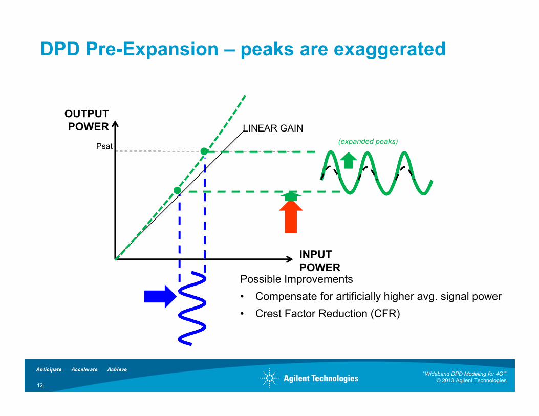
DPD Net Result: Linear gain of complex-valued RF
carrier envelope over a specific range of power levels
LINEAR
INPUT
POWER
OUTPUT
POWER
DPD pre-expanded peaks
INPUT
POWER
PA compresses peaksLINEAR
Baseband Digital Pre-Distortion
RF Power Amplification
“Wideband DPD Modeling for 4G””© 2013 Agilent Technologies

What does a DPD look like? (Volterra Model)
14
∑=
=K
k
k nznz1
)()( ∑ ∑ ∏= = =
−=
Q
m
Q
m
k
l
lkkk
k
mnymmhnz0 0 1
1
1
)(),,()( LL
∑∑∑= ==
+−−+−+=
Q
m
Q
m
Q
m
mnymnymmhmnymhhnz0 0
21212
0
1110
1 21
)()(),()()()( K
Volterra series pre-distorter can be described by
where
Which is a 2-dimensional summation of power series & past time envelope responses
A full Volterra produces a huge computational load. People usually simplify it into
• Wiener model • Hammerstein model • Wiener-Hammerstein model• Memory polynomial model
“Wideband DPD Modeling for 4G””© 2013 Agilent Technologies

15
DPD principles – Memory Polynomial Model
If only diagonal terms are kept, Volterra reduces to “Memory polynomial” model.
Agilent uses the “Indirect Learning” algorithm to extract MP coefficients.
You can now add your own model, extraction algorithm, and even your own GUI.
L. Ding, G. T. Zhou, D. R. Morgan, Z. Ma, J. S. Kenney, J. Kim, and C. R. Giardina, “Memory
polynomial predistorter based on the indirect learning architecture,” in Proc. of GLOBECOM, Taipei, Taiwan, 2002, vol. 1, pp. 967–971.
∑∑= =
−−−=
K
k
Q
q
k
kq qnyqnyanz1 0
1)()()(
Where• K is Nonlinearity order • Q is Memory length
“Wideband DPD Modeling for 4G””© 2013 Agilent Technologies

16
Agenda
1. Introduction and Problem Statement
2. Digital Pre-Distortion (DPD) Concepts
3. DPD verification with Agilent Hardware
4. DPD simulation with Agilent EDA Tools
5. Crest Factor Reduction (CFR)
6. Summary
“Wideband DPD Modeling for 4G””© 2013 Agilent Technologies

Generalized Wireless Transmitter Path
BB PHY
CFR DPDUp
convertPA
EnvTracking
DAC
Downconvert
ADCAdapt
Duplexer
• Which blocks are included with your final product?• What IP do you have access to? Or, are able to imitate? Able to modify?• What final system specifications do you need to test against?
17
?
??
?
??
“Wideband DPD Modeling for 4G””© 2013 Agilent Technologies

Vector Signal
Analyzer
MXA, PXA, Modular
Agilent Measurement-based DPD Modeling Platform
BB TX PHY
CFRDPD
model
Upconvert
PADAC
Downconvert
ADCGenerate
Coefficients
Vector Signal
Generator
AWGESG, MXG, PSG
W1716
DPD
Step-by-Step GUI
W1918
LTE-A
IP Library
BB RXPHY
Throughput
BER/FER
ACPR
EVM
89600 VSA
Optional Reference RX
W1461 SystemVue
Also:
3G, WLAN60GHz,
DVB, OFDM
18
“Wideband DPD Modeling for 4G””© 2013 Agilent Technologies

Measurement-Based DPD Modeling Flow
Method 1 – Measure both PA Input and Output signals
Get baseband complex waveforms of
PA input and output
Extract DPD Model (includes delay estimation
and adjustment)
Apply DPD Model, and Get DPD+PA Response
Verify DPD Performance
Create DPD Stimulus
RF Input RF Output
11
55
44
33
22
Adjust current to
control switch
Switch
MXA / PXA
MXG
Power Splitter
DC Power Analyzer
DUT
THRU
19
“Wideband DPD Modeling for 4G””© 2013 Agilent Technologies

20
Measurement-Based DPD Modeling Flow
Method 1 – Measure both PA Input and Output signals
• DPD flow consists of 5 steps in SystemVue • Convergence improves with more iterations • 2-3 iterations are typical for real PAs
Get baseband complex waveforms of
PA input and output
Extract DPD Model (includes delay estimation
and adjustment)
Apply DPD Model, and Get DPD+PA Response
Verify DPD Performance
Create DPD Stimulus
RF Input RF Output
11
55
44
33
22
“Wideband DPD Modeling for 4G””© 2013 Agilent Technologies

Measurement-Based DPD Modeling Simplification:
Calculated PA Input, Measured PA Output
Single connection allows automation, iterationsEliminates one measurement, physically fasterIdentical extraction algorithms, verification process
MXA / PXAMXG
DUT
21
“Wideband DPD Modeling for 4G””© 2013 Agilent Technologies
Get baseband complex waveforms of
PA input and output
Extract DPD Model (includes delay estimation
and adjustment)
Apply DPD Model, andGet DPD+PA Response
Verify DPD Performance
Create DPD Stimulus
Simulated
BB Input
Meas RF
Output
11
55
44
33
22

22
Measurement-Based DPD Modeling Simplification:
Calculated PA Input, Measured PA Output
• Uses the Ideal BB stimulus waveform vs. measured PA output waveform to extract the DPD model.
• Advantages:- Single connection- PA remains “ON”- Easier to automate- Faster speed
• Is typical of industry practice today
• Linearizes the entire system, not just the PA
• Provides very acceptable accuracy for quick Evaluation and MFG Test applications.
• Assumptions:- Source flatness- Source linearity- No additional source
signal conditioning
Get baseband complex waveforms of
PA input and output
Extract DPD Model (includes delay estimation
and adjustment)
Apply DPD Model, andGet DPD+PA Response
Verify DPD Performance
Create DPD Stimulus
Simulated
BB Input
Meas RF
Output
11
55
44
33
22
“Wideband DPD Modeling for 4G””© 2013 Agilent Technologies

Comparing Methods: BB Input vs. Measured RF
ACLR -2BW
Lower
-1BW
Lower
+1BW
Upper
+2BW
Upper
Raw PA output
54.06 35.33 35.68 53.58
DPD+PA w/ BB input
55.05 50.15 52.28 54.59
DPD+PA w/ PA input
55.80 51.23 54.32 55.41
LTE-Advanced DL (20 MHz) 6-Carrier GSM
ACLR of DL 20 MHz System
Measured RF input
BB input DPD+PA
RESULTS
23
“Wideband DPD Modeling for 4G””© 2013 Agilent Technologies

SystemVue DPD Modeling Flow for LTE/LTE-A
The download power and length of the waveform can also be set.
24
Step 1. Create DPD stimulus waveform• Set LTE parameters such as BW, Resource Block allocation and others• Choose between built-in LTE or LTE-Advanced waveform generation
“Wideband DPD Modeling for 4G””© 2013 Agilent Technologies

THRU : Connect the MXG/AWG directly to the PXA/M9392A and click the “Capture Waveform” button. This is the true RF PA input.
DUT: Connect the MXG to the PA, connect the PA to the PXA/M9392A, and click the “Capture Waveform” button. The captured signal is the output of the PA DUT.
The measured I/Q files are stored and used in following steps.
25
Step 2. Capture PA response• SystemVue downloads directly to the MXG or M9330A AWG (source), and
capture data back from PXA or M9392A (analyzer).• Equipment parameters such as number of signal, trace assignment, and file
name can be set.
SystemVue DPD Modeling Flow for LTE/LTE-A
“Wideband DPD Modeling for 4G””© 2013 Agilent Technologies

DPD AM-to-AM Characteristic
26
SystemVue DPD Modeling Flow for LTE/LTE-A
Step 3. DPD Model Extraction• DPD model parameters such as number
of training samples, memory order, and nonlinear order can be set.
PA AM-to-AM Characteristic
“Wideband DPD Modeling for 4G””© 2013 Agilent Technologies

27
SystemVue DPD Modeling Flow for LTE/LTE-A
Step 4. Capture DPD+PA Response• The signal is pre-distorted by the DPD model
and re-downloaded into the MXG or AWG.
DPD+PA (measured RF output)
PA input (original RF input)
Set the RF powerDPD+PA AM-to-AM Characteristic
“Wideband DPD Modeling for 4G””© 2013 Agilent Technologies

SystemVue DPD Modeling Flow for LTE/LTE-A
Step 5. Verify DPD+PA response• LTE performance for the DPD model used with the PA hardware is verified.
Spectrum, EVM andACLR are calculatedand plotted automatically
28
“Wideband DPD Modeling for 4G””© 2013 Agilent Technologies

29
Accommodating Proprietary IP
• Use your own extractor IP instead of Agilent’s • Continue to enjoy an integrated environment• Allows remote & distributed DPD teamwork • Greater user control of algorithm details, IP
security, performance, delivery date, quality, etc
Custom DPD Model Extraction(.m math language)
Custom Digital Pre-distorter(.m math language)
“Wideband DPD Modeling for 4G””© 2013 Agilent Technologies

DPD of LTE-Advanced DL with Doherty PA (200W)Spectrum, ACLR and EVM results (10 MHz DL System)
ACLR -2BW
Lower
-1BW
Lower
+1BW
Upper
+2BW
Upper
BB input (sim)
58.67 49.63 49.17 58.01
Raw PA output
49.90 28.69 28.35 47.31
DPD+PA
output
48.88 45.10 45.16 48.83
ACLR (dB)
EVM
EVM (%) EVM (dB)
Simulation BB input 5.33 -24.46
Raw PA output 10.13 -19.89
DPD+PA output 5.52 -25.16
CFR was applied to this LTE-Advanced DL signal, with a
maximum EVM target of 10% for 16-QAM.
Raw PA output
PA+DPD, after 1 iteration to extract DPD coefficients
30
RF Vector Source:N5182B MXGRF Vector Analyzer: N9030A PXA
“Wideband DPD Modeling for 4G””© 2013 Agilent Technologies

DPD of LTE-Advanced DL with Doherty PA (200W)Spectrum, ACLR and EVM results (20MHz DL System)
ACLR -2BW
Lower
-1BW
Lower
+1BW
Upper
+2BW
Upper
BB input (sim)
64.73 55.09 57.10 64.92
Raw PA output
51.01 30.69 30.04 49.50
DPD+PA
output
50.31 45.16 45.56 51.40
ACLR (dB)
EVM
EVM (%) EVM (dB)
BB input signal (sim) 6.10 -24.28
Raw PA output 8.87 -21.04
DPD+PA output 6.88 -23.24
CFR was applied to this LTE-Advanced DL signal with a maximum EVM
target of 10%,8% and 6% for QPSK, 16-QAM and 64-QAM, respectively.
Raw PA output
PA+DPD, after 1 iteration to extract DPD coefficients
31
RF Vector Source:N5182B MXGRF Vector Analyzer: N9030A PXA
“Wideband DPD Modeling for 4G””© 2013 Agilent Technologies

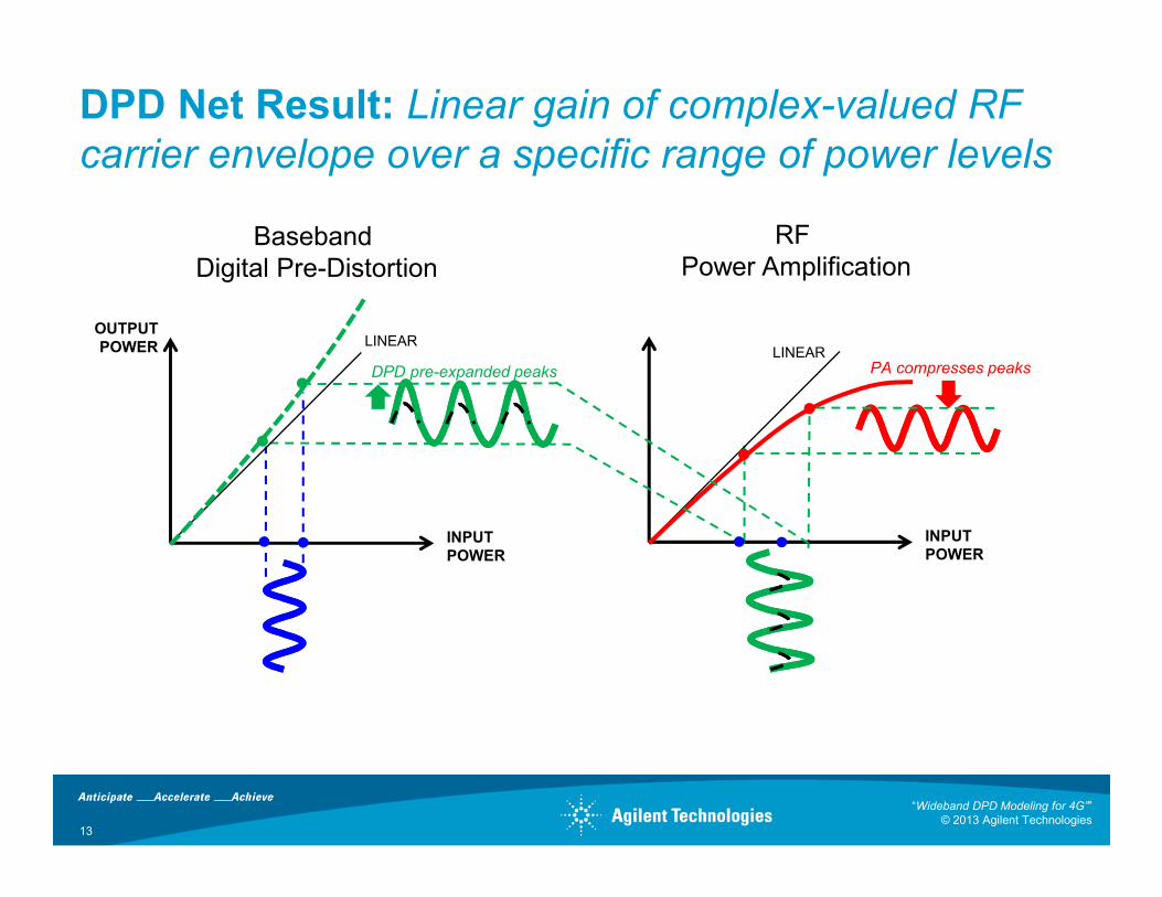
LTE-A Results with 200W LDMOS Doherty PARaw PA Output (DL 20MHz System)
32
“Wideband DPD Modeling for 4G””© 2013 Agilent Technologies
LTE-A Results with 200W LDMOS Doherty PADPD+PA Output (DL 20MHz System)
33
“Wideband DPD Modeling for 4G””© 2013 Agilent Technologies

ACLR (dB)
CC0 EVM (QPSK)
CC1 EVM (16-QAM)
LTE-A Results with 200W LDMOS Doherty PAResults with (2x10MHz) Carrier Aggregation of 2 separate CC’s
ACLR -2BW
Lower
-1BW
Lower
+1BW
Upper
+2BW
Upper
BB input (sim)
63.11 56.75 56.70 62.72
Raw PA output
50.58 30.80 30.22 49.06
DPD+PA
output
51.74 45.75 45.73 51.18
EVM (%) EVM (dB)
Baseband signal (sim) 0.21 -53.43
Raw PA output 3.03 -30.37
DPD+PA output 1.93 -34.28
EVM (%) EVM (dB)
Baseband signal (sim) 0.20 -54.11
Raw PA output 3.12 -30.11
DPD+PA output 1.93 -34.31
Raw PA output
PA+DPD, after 1 iteration to extract DPD coefficients
34
RF Vector Source:N5182B MXGRF Vector Analyzer: N9030A PXA
“Wideband DPD Modeling for 4G””© 2013 Agilent Technologies

Multi-Standard Radio (MSR) into Doherty PA (200W)
2 CarriersGSM
2 Carriers WCDMA
2 Carriers LTE
2 Carriers EDGE
Raw PA output
PA+DPD
35
“Wideband DPD Modeling for 4G””© 2013 Agilent Technologies

Example 2: Efficiency vs. Distortion (20W Doherty)2x50W devices, Fc=2.14 GHz, LTE=20MHz, PAPR=7.3dB
Vgs1: +3.05V Vgs2=1.8V Idqs: 434mA Vds: +28V
Transistor: MRF6S21050 FreeScale 50W x 2
“Wideband DPD Modeling for 4G””© 2013 Agilent Technologies
36
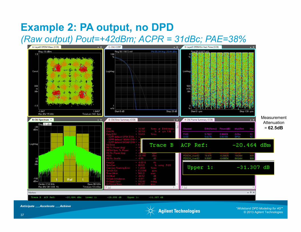
Example 2: PA output, no DPD (Raw output) Pout=+42dBm; ACPR = 31dBc; PAE=38%
MeasurementAttenuation
= 62.5dB
“Wideband DPD Modeling for 4G””© 2013 Agilent Technologies
37

Example 2: PA output, with DPD(Full power) Pout=+42dBm; ACPR = 31dBc; PAE=39%
“Wideband DPD Modeling for 4G””© 2013 Agilent Technologies
38

Example 2 Summary: No DPD vs. DPD
Doherty PA 50W x2, Freq 2.14GHz
LTE 20MHz,
PAPR 7.3dB with CFR
PA Output
Without DPD
PA Output
With DPD
Improve-
ment
Output Power +42dBm (15.8W) +42dBm(15.8W) 0
Gain 13.5 dB 13.5 dB 0
ACPR Lower ACPR: -30.0 dBc
Upper ACPR: -31.3 dBc
Lower ACPR: -45.2dBc
Upper ACPR: -45.1 dBc
15 dB
EVM QPSK: 10.6%
16QAM: 10.8%
64QAM: 9.9%
QPSK: 6.6%
16QAM: 6.8%
64QAM: 6.7%
3.8%
Efficiency 38% 39% +1%
Memory Effect 1.4 dB 0.04 dB 1.3 dB
“Wideband DPD Modeling for 4G””© 2013 Agilent Technologies
39

Example 2: PA output, no DPD(Backed off 10dB) Pout=+33dBm; ACPR > 45dBc; PAE=12%
“Wideband DPD Modeling for 4G””© 2013 Agilent Technologies
40

Example 2 Summary: 10dB Back-off vs. DPD
Doherty PA 50W x2, Freq 2.14GHz
LTE 20MHz,
PAPR 7.3dB with CFR
PA Output
Backed off 10dB to meet
ACLR=45dB spec
PA Output
With DPD
Specificati
on
Improved
Output Power +33dBm (2W) +42dBm (15.8W) +9dB
Gain 16 dB 13.5 dB -2.5dB
ACPR Lower ACPR: -45.6 dBc
Upper ACPR: -45.3 dBc
Lower ACPR: -45.2 dBc
Upper ACPR: -45.1 dBc
0 dB
EVM QPSK: 6.7%
16QAM: 6.9%
64QAM: 6.7%
QPSK: 6.6%
16QAM: 6.8%
64QAM: 6.7%
0%
Efficiency 12% 39% +27%
Memory Effect 0.3 dB 0.04 dB 0.3 dB
“Wideband DPD Modeling for 4G””© 2013 Agilent Technologies
41

Example 3: LTE-Advanced, 2CC 40MHzContiguous Carrier Aggregation, with CFR
19-22dB
RF Source: N5182B MXG or M9381A VSGRF Vector Analyzer:N9030A PXA
“Wideband DPD Modeling for 4G””© 2013 Agilent Technologies
42

Example 3: LTE-A 2CC 40MHzPA Input (EVM=6.1%, ACPR=60.1dB, PAPR=6.90dB)
“Wideband DPD Modeling for 4G””© 2013 Agilent Technologies
43

Example 3: LTE-A 2CC 40MHzPA Output (EVM=8.3%, ACPR=34.0dB, PAPR=5.82dB)
“Wideband DPD Modeling for 4G””© 2013 Agilent Technologies
44

Example 3: LTE-A 2CC 40MHzDPD+PA Output (Iter #1, EVM=6.1%, ACPR=52.8dB, PAPR=6.90dB)
“Wideband DPD Modeling for 4G””© 2013 Agilent Technologies
45
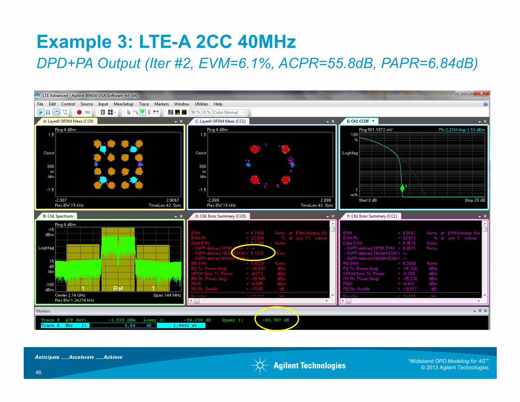
Example 3: LTE-A 2CC 40MHzDPD+PA Output (Iter #2, EVM=6.1%, ACPR=55.8dB, PAPR=6.84dB)
“Wideband DPD Modeling for 4G””© 2013 Agilent Technologies
46

ACPR (dB) EVM (%)
Lower Upper CC0 CC1
PA Input -60.46 -60.13 6.13% 6.10%
PA Output -33.57 -34.01 8.26% 8.13%
DPD+PA
Output Iter 1 -52.60 -52.85 6.09% 6.04%
DPD+PA
Output Iter 2 -55.27 -55.80 6.15% 6.07%
Example 3 Summary: LTE-A 2CC 40MHz
~21.8dB final improvement
“Wideband DPD Modeling for 4G””© 2013 Agilent Technologies
47

Example 4: 802.11ac 5GHz WLAN 80MHz with CFR (PAPR=7dB)
11-14dB
RF Source:N8241A AWG + E8257D PSGVector Analyzer:M9392A PXI VSA
“Wideband DPD Modeling for 4G””© 2013 Agilent Technologies
48

ACPR (dB) EVM
Lower Upper EVM % EVM dB
PA input -46.45 -46.18 6.71% -23.47 dB
PA output -34.91 -34.79 8.68% -21.23 dB
DPD+PA
output
-46.29 -45.39 6.97% -23.13 dB
Example 4 Summary: 802.11ac 5GHz WLAN 80MHz with CFR (PAPR=7dB)
~11dB final improvement
“Wideband DPD Modeling for 4G””© 2013 Agilent Technologies
49

802.11ac 80MHz with CFR (PAPR=7dB) PA Input
“Wideband DPD Modeling for 4G””© 2013 Agilent Technologies
50

802.11ac 80MHz with CFR (PAPR=7dB) PA Output
“Wideband DPD Modeling for 4G””© 2013 Agilent Technologies
51

802.11ac 80MHz with CFR (PAPR=7dB) DPD+PA Output
“Wideband DPD Modeling for 4G””© 2013 Agilent Technologies
52

53
Agenda
1. Introduction and Problem Statement
2. Digital Pre-Distortion (DPD) Concepts
3. DPD verification with Agilent Hardware
4. DPD simulation with Agilent EDA Tools
5. Crest Factor Reduction (CFR)
6. Summary
“Wideband DPD Modeling for 4G””© 2013 Agilent Technologies
54
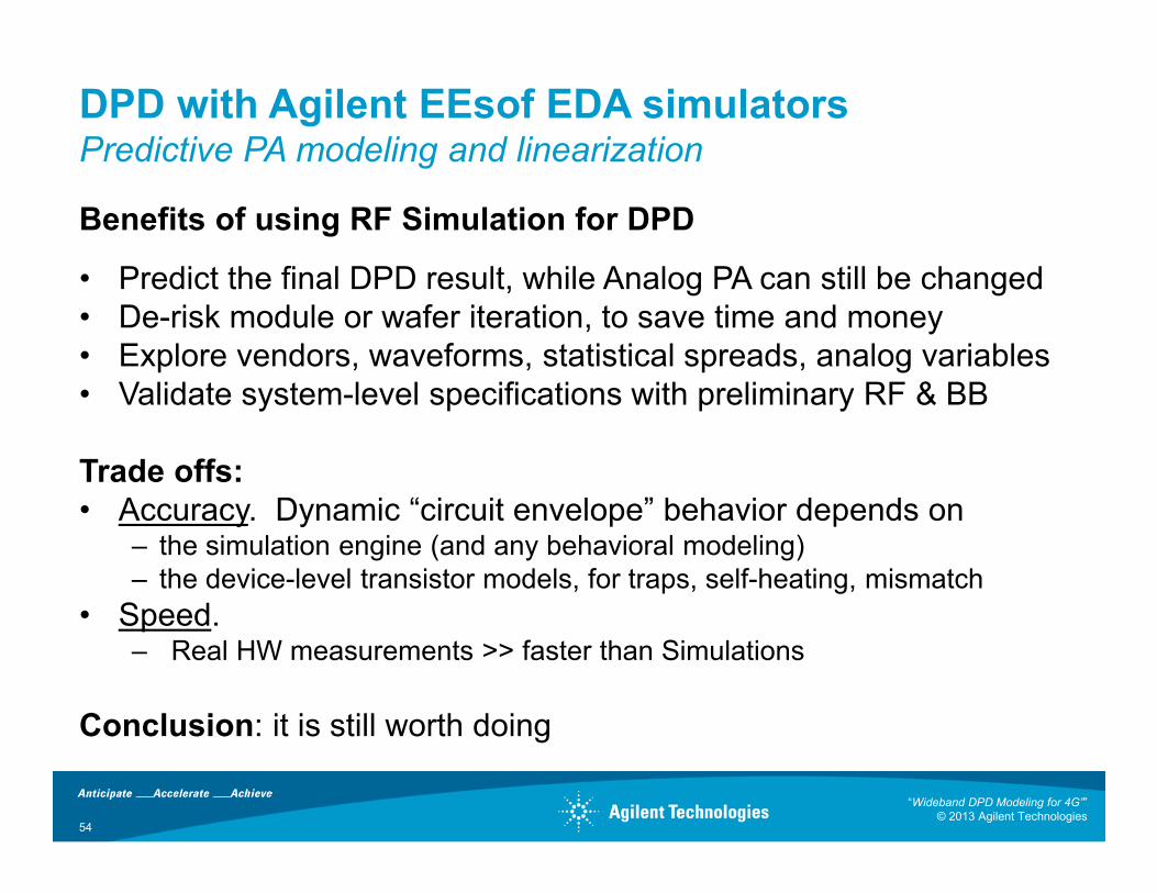
DPD with Agilent EEsof EDA simulatorsPredictive PA modeling and linearization
Benefits of using RF Simulation for DPD
• Predict the final DPD result, while Analog PA can still be changed • De-risk module or wafer iteration, to save time and money• Explore vendors, waveforms, statistical spreads, analog variables• Validate system-level specifications with preliminary RF & BB
Trade offs:
• Accuracy. Dynamic “circuit envelope” behavior depends on– the simulation engine (and any behavioral modeling)– the device-level transistor models, for traps, self-heating, mismatch
• Speed. – Real HW measurements >> faster than Simulations
Conclusion: it is still worth doing
“Wideband DPD Modeling for 4G””© 2013 Agilent Technologies

Simulation vs. Measurement DPD Extraction
55
• ADS & GoldenGate Circuits as simulated RF DUTs- Complex loading, memory FX, dynamic behaviors
• NVNA X-parameter measurement model,- Great for smaller solid-state devices
SIMULATION-BASED DPD
(predictive)
X-parametersX-parameters
CO-SIM, MODELS
CO-SIM, MODELS
MODEL
ADS
GG
RF DUTN5241,2 PNA-X
External Trigger
Attenuator
N5182 MXG, or E8257D PSG
as external modulatorM9330A AWG if > 100 MHz
89600
VSA
89600
VSA
M9392A PXI VSA (>140MHz)or N9030A PXA (<140 MHz)
I,Q RF
RF DUT
MEASUREMENT-BASED DPD
“Wideband DPD Modeling for 4G””© 2013 Agilent Technologies

Generalized Wireless Transmitter Path
BB PHY
CFR DPDUp
convertPA
EnvTracking
DAC
Downconvert
ADCAdapt
Duplexer
• Which blocks are included with your final product?• What IP do you have access to? Or, are able to imitate? Able to modify?• What final system specifications do you need to test against?
56
?
??
?
??
“Wideband DPD Modeling for 4G””© 2013 Agilent Technologies

Agilent Simulation-based DPD Modeling Platform
BB TX PHY
CFRDPD
model
Upconvert
PADAC
Downconvert
ADCGenerate
Coefficients
W1716
DPD
Step-by-Step GUI
W1918
LTE-A
IP Library
BB RXPHY
Throughput
BER/FER
ACPR
EVM
89600 VSA
Optional Reference RX
W1461 SystemVue
Also:
3G, WLAN60GHz,
DVB, OFDM
Agilent ADS
Agilent GoldenGate
RF circuit-level EDA software
57
“Wideband DPD Modeling for 4G””© 2013 Agilent Technologies

Simulation-based, predictive DPDSystemVue co-simulation with circuit-level PA in ADS
EnvOutSelector
O1
OutFreq=FCarrier
GainRF
G4
Gain=1
SVCosimSinkTimed
S3
SVReceiverID="ADSToSystemVue"BlockSize="BlockSize"
in put
SVCosimSourceTimed
S4
SVSenderID="SystemVueToADS"
TimeStep="Tstep"
Fc="FCarrier"BlockSize="BlockSize"
o utp ut
DF
DF
Vdc
FETLS12_MWTD_FETMGA_545P8_FET2
datafile=myfile
Fingers=14Width=1020 um
FETLS12_MWTD_FETMGA_545P8_FET1
datafile=myfile
Fingers=1Width=32 um
VARVAR3
myfile=strcat(mypath,"/adsptolemy/lib/data/bdaa.txt")mypath=echo("$HPEESOF_DIR")
EqnVar
I_ProbeI_in1
I_Probe
Ig
I_ProbeIout
I_Probe
I_d
MSUB
MSub1
TanD=0.03T=2 mil
Hu=3.9e+034 milCond=1.0E+50
Mur=1Er=4.6
H=10.0 mil
MSub
VARVAR2
Cout=10Rout=50
Rbias=655N=2.75
Fin=5.5Pwrin=13
Eqn
Var
MLOCTL3
W=16.0 milSubst="MSub1"
MLOC
TL2
W=16.0 mil
Subst="MSub1"
Port
P1Num=1
Port
P2Num=2
MLIN
TL6
L=100.0 milW=16 mil
Subst="MSub1"
MLIN
TL5
L=100.0 milW=16 mil
Subst="MSub1"
MLINTL4
L=100.0 mil
W=16 milSubst="MSub1"
MLIN
TL1
L=100.0 milW=16 mil
Subst="MSub1"
CC31
C=3.3 pF
C
C25C=2.2 pF
LL35
R=L=.13 nH
MTEETee2
W3=16 milW2=16 mil
W1=16 milSubst="MSub1"
MTEETee1
W3=16 milW2=16 mil
W1=16 milSubst="MSub1"
RR2
R=42 OhmCC32
C=1.5 pF
LL14
R=L=3.9 nH
RR1R=655 Ohm
ADS circuit-level PA(circuit envelope simulation)
ADS Ptolemy(circuit-system co-simulation)
SystemVueSTIMULUS
SystemVueRESPONSE
CO-SIM CO-SIM
ADS reads data
from SystemVueADS sends data
to SystemVue
ADS circuit-level
PA,needs Circuit Envelop
to co-simulate
with SystemVue.
58
“Wideband DPD Modeling for 4G””© 2013 Agilent Technologies

Simulation-based, predictive DPDSystemVue co-simulation with circuit-level PA in ADS
Re
Im
R1
Ga in=0.978 [PowerAl ignm ent]
G1
Pe riodic =YES
Fi le= ' Step3_DPD_Coe ffi c ients _Rea l_ Iter2.tx t [DPD_Co effi c ien ts_Real_Fi leName]
Fi le= 'Step1_BBDa ta_ Im ag_Iter1 .tx t [Step1_BBData_Im a g_Fi leName]
R8
Fc
CxEnv
E2
T
Sam p leRa te=69 .33e+6Hz [Sam p lingRate]
S4
Segm en tTim e=50µs
Sta rt=0s
Re
Im
C1
DPD_Pr eDist ort erDPD_I nput
DPD_Coef
DPD_O ut put
Num OfInpu tSam ples=20000 [Num OfInpu tSam ples]
Nonl inea rOrde r=9 [Non linea rOrde r]
M em oryOrder=5 [M em ory Orde r]
D1
Fc
EnvCx
Fc =2 .505GHz [FCa rrie r]
C2
ADS Cos im
OutputID=' ADSToSys tem Vue
InputID=' Sy s tem VueToADS
OutputBlock Siz e=1000 [Bloc kSize]
InputBloc kSiz e=1000 [Bloc kSize]
Ou tpu tFc=2.505e+9 [FCarrier]
A1
Da taFileNam e=' Step4_DPD_PAOutputdata_ Im ag_ Ite r2 .tx t [Step4_DPD_PAOu tpu t_ Im ag_Fi leNam e ]
Sam pleStop=99998 [StopSam p le- 1]
Sam p leSta rt=0 [Sta rtSam ple ]
StartStopOption=Sam ples
123
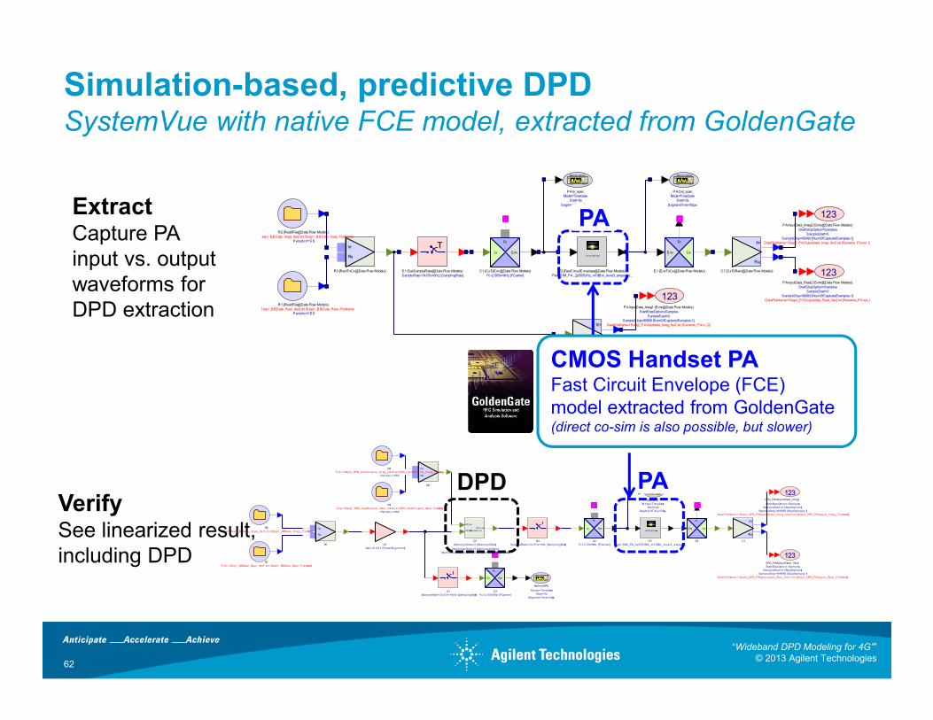
ExtractCapture PA input vs. output waveforms for DPD extraction
VerifySee linearized result, including DPD
Re
Im
C7 CxToRect@Data Flow Models
Fc
CxEnv
E1 EnvToCx@Data Flow Models
Fc
EnvCx
Fc=2.505e+9Hz [FCarrier]C1 CxToEnv@Data Flow Models
T
SampleRate=69.33e+6Hz [SamplingRate]S1 SetSampleRate@Data Flow Models
Re
Im
R3 RectToCx@Data Flow Models
R1 ReadFile@Data Flow Models
Periodic=YES
File='Step1_BBData_Imag_Iter2.txt [Step1_BBData_Imag_FileName ]
R2 ReadFile@Data Flow Models
123
DataFileName='Step2_PAOutputdata_Real_Iter2.txt [filename_PAout_I]SampleStop=99999 [NumOfCapturedSamples-1]
SampleStart=0
StartStopOption=Samples
PAInputData_Real2 Sink@Data Flow Models
123
DataFileName='Step2_PAOutputdata_Imag_Iter2.txt [filename_PAout_Q]
SampleStop=99999 [NumOfCapturedSamples-1]SampleStart=0
StartStopOption=Samples
PAInputData_Imag2 Sink@Data Flow Models
ADS Cos im
OutputID='ADSToSystemVue
InputID='SystemVueToADSOutputBlockSize=1000 [B lockSize]
InputBlockSize=1000 [BlockSize]
OutputFc=2.505e+9 [FCarrier]A1 ADSCosimBlockEnv@Data Flow Models
SystemVue
DPDSystemVue
PA
ADS
PA
ADS
The UI to connect with ADS in SystemVue, corresponding to the schematic (Ptolemy co-sim with circuit-level design) in ADS.
59
“Wideband DPD Modeling for 4G””© 2013 Agilent Technologies

60
Simulation-based, predictive DPDSystemVue co-simulation with circuit-level PA in ADS
40dB improvement after 2 iterations
6-Carrier GSMCarrier Spacing: 4MHz
Sampling Rate:256 * 270.8333kHz =69.3333 MHz
PA input Spectrum (Green)PA output Spectrum(Blue)PA+DPD Spectrum (Red, first iteration)PA+DPD Spectrum (Orange, Second iteration)
“Wideband DPD Modeling for 4G””© 2013 Agilent Technologies

Envelope Tracking (ET): Using ADS “Circuit
Envelope” to improve true modulated PAE
61
For more information about this application see blog article:http://www.rf-design-tips.com/envelope-tracking-simulation/
“Wideband DPD Modeling for 4G””© 2013 Agilent Technologies
Re
Im
R6
Re
Im
R1
Gain=0 .821 [PowerAl ignm ent]
G1
Period ic =YES
Fi le='Step3_DPD_Coe ffic ients _Rea l_Iter2.tx t [DPD_Co effic ien ts _Rea l_Fi leName]
R4
Period ic =YES
Fi le= 'Step3_DPD_Coeffic ien ts _Im ag_Iter2.tx t [DPD_Co effic ien ts _Im ag_Fi leName]
R5
Fi l e= 'Step1_BBDa ta_ Im ag_Iter1.tx t [Step1_BBDa ta_ Im ag_Fi leName]
R8
Fi l e= 'Step1_BBDa ta_Real _Iter1 .tx t [Step1_BBData_Real_Fi leName]
R7
Fc
CxEnv
E2
Fc
EnvCx
Fc =2.505GHz [FCa rrie r]
C2
Fast Cir cuit Envelope
Fi l e= 'SIM_PA_2p505GHz _m 7dBm _lev e l3_ampaccu...
F2
T
Sam pl eRate=34.67e+6Hz [Samp l ingRate]
S4
Spect rum Anal yzer
Segm en tTim e=50µs
Start=0s
M ode=Tim eGate
AfterDPD
Re
Im
C1
Fc
EnvCx
Fc =2.505GHz [FCa rrie r]
C3
Spect r um Anal yzer
SegmentTim e=50µs
Sta rt=0s
M ode=Tim eGa te
Be fo reDPD
T
Sam pleRa te=34.67e+6Hz [Sam p l ingRate]
S1
DPD_Pr eDist or t erDPD_I nput
DPD_Coef
DPD_O ut put
NumOfInpu tSam pl es =30000 [Num OfInputSamp les]
Nonl i nearOrder=9 [Nonl inearOrder]
M em ory Order=5 [M em ory Orde r]
D1
123
DataFi leName=' Step4_DPD_PAOutpu tda ta_Im ag_ Ite r2.tx t [Step4_DPD_PAOu tput_ Im ag_Fi leName]
Sam pl eStop=99998 [StopSam pl e- 1]
Sam p leSta rt=0 [Sta rtSam p le]
StartStopOp tion=Samp les
DPD_PAOu tputData_ Im ag
123
DataFi leName=' Step4_DPD_PAOutpu tda ta_Rea l_Iter2.tx t [Step4_DPD_PAOu tpu t_Real_Fi leName]
Sam pl eStop=99998 [StopSam pl e- 1]
Sam p leSta rt=0 [Sta rtSam p le]
StartStopOp tion=Samp les
DPD_PAOutputDa ta_Real
Re
Im
C7 CxToRect@Data Flow Models
Fc
CxEnv
E1 EnvToCx@Data Flow Models
Fc
EnvCx
Fc=2.505e+9Hz [FCarrier]
C1 CxToEnv@Data Flow Models
T
SampleRate=34.67e+6Hz [SamplingRate]
S1 SetSampleRate@Data Flow Models
Re
Im
R3 RectToCx@Data Flow Models
Periodic=YES
File='Step1_BBData_Real_Iter2.txt [Step1_BBData_Real_FileName]
R1 ReadFile@Data Flow Models
Periodic=YES
File='Step1_BBData_Imag_Iter2.txt [Step1_BBData_Imag_FileName ]
R2 ReadFile@Data Flow Models
123
DataFileName='Step2_PAOutputdata_Real_Iter2.txt [filename_PAout_I]
SampleStop=99999 [NumOfCapturedSamples-1]
SampleStart=0
StartStopOption=Samples
PAInputData_Real2 Sink@Data Flow Models
123
DataFileName='Step2_PAOutputdata_Imag_Iter2.txt [filename_PAout_Q]
SampleStop=99999 [NumOfCapturedSamples-1]
SampleStart=0
StartStopOption=Samples
PAInputData_Imag2 Sink@Data Flow Models
Fast Cir cuit Envelope
File='SIM_PA_2p505GHz_m7dBm_level3_ampaccu...
F2 FastCircuitEnvelope@Data Flow Models
Re
Im
C2 CxToRect@Data Flow Models 123
DataFileName='Step2_PAInputdata_Real_Iter2.txt [filename_PAin_I]
SampleStop=99999 [NumOfCapturedSamples-1]
SampleStart=0
StartStopOption=Samples
PAInputData_Real1 Sink@Data Flow Models
123
DataFileName='Step2_PAInputdata_Imag_Iter2.txt [filename_PAin_Q]
SampleStop=99999 [NumOfCapturedSamples-1]
SampleStart=0
StartStopOption=Samples
PAInputData_Imag1 Sink@Data Flow Models
Spect rum Anal yzer
SegmentTime=50µs
Start=0s
Mode=TimeGate
PAOut_spec
Spect r um Anal yzer
SegmentTime=50µs
Start=0s
Mode=TimeGate
PAIn_spec
PA
Simulation-based, predictive DPDSystemVue with native FCE model, extracted from GoldenGate
CMOS Handset PAFast Circuit Envelope (FCE) model extracted from GoldenGate (direct co-sim is also possible, but slower)
DPD PA
ExtractCapture PA input vs. output waveforms for DPD extraction
VerifySee linearized result, including DPD
62
“Wideband DPD Modeling for 4G””© 2013 Agilent Technologies

Simulation-based, predictive DPDSystemVue with native FCE model, extracted from GoldenGate
30dB improvementafter 2 iterations
6-Carrier GSMCarrier Spacing: 600kHz
Sampling Rate:128 * 270.8333kHz=34.6667 MHz
PA input Spectrum (Green)PA output Spectrum(Blue)PA+DPD Spectrum (Red, first iteration)PA+DPD Spectrum (Orange, Second iteration)
63
“Wideband DPD Modeling for 4G””© 2013 Agilent Technologies

Simulation-based, predictive DPDSystemVue with analog X-parameter model (100W PA)
Analog X-parameter device is placed into a Spectrasys subnetwork (RF simulation domain)
Source1=200 MHz at -10 dBm
MultiSource_3 MultiSourceZO=50Ω
Port_2 *OUT
*GND
VDC=22V
SG1 VDC
X1
2
3VDC
File='.\100W_3Hz_3H_3Bias_PHD.mdf
XP_1 XPARAMS
FILE
64
“Wideband DPD Modeling for 4G””© 2013 Agilent Technologies

Re
Im
C7 CxToRect@Data Flow Models
Fc
CxEnv
E1 EnvToCx@Data Flow Models
Fc
EnvCx
Fc=200e+6Hz [FCarrier]
C1 CxToEnv@Data Flow Models
T
SampleRate=34.67e+6Hz [SamplingRate]
S1 SetSampleRate@Data Flow Models
Re
Im
R3 RectToCx@Data Flow Models
Periodic=YES
File='Step1_BBData_Real_Iter1.txt [Step1_BBData_Real_FileName]R1 ReadFile@Data Flow Models
Periodic=YESFile='Step1_BBData_Imag_Iter1.txt [Step1_BBData_Imag_FileName ]
R2 ReadFile@Data Flow Models
123
DataFileName='Step2_PAOutputdata_Real_Iter1.txt [filename_PAout_I]
SampleStop=99999 [NumOfCapturedSamples-1]SampleStart=0
StartStopOption=Samples
PAInputData_Real2 Sink@Data Flow Models
123
DataFileName='Step2_PAOutputdata_Imag_Iter1.txt [filename_PAout_Q]
SampleStop=99999 [NumOfCapturedSamples-1]
SampleStart=0StartStopOption=Samples
PAInputData_Imag2 Sink@Data Flow Models
RF_Link
CalcPhaseNoise=NO
EnableNoise=NOFreqSweepSetup=Automatic
Schematic='Xparam_device
Data1 RF_Link@Data Flow Models
Spect rum Anal yzer
SegmentTime=50µs
Start=0sMode=TimeGate
PAOut_spec
Spect rum Anal yzer
SegmentTime=50µs
Start=0sMode=TimeGate
PAIn_spec
Re
Im
C2 CxToRect@Data Flow Models
123
DataFileName='Step2_PAInputdata_Real_Iter1.txt [filename_PAin_I]
SampleStop=99999 [NumOfCapturedSamples-1]
SampleStart=0StartStopOption=Samples
PAInputData_Real1 Sink@Data Flow Models
123
DataFileName='Step2_PAInputdata_Imag_Iter1.txt [filename_PAin_Q]SampleStop=99999 [NumOfCapturedSamples-1]
SampleStart=0
StartStopOption=SamplesPAInputData_Imag1 Sink@Data Flow Models
Simulation-based, predictive DPDSystemVue with analog X-parameter model (100W PA)
Re
Im
R6
Ga in=1.14 [PowerAl ignm ent]
G1
Periodic =YES
Fi le='Step3_DPD_Coe ffic ients _Rea l_ Ite r1.tx t [DPD_Coe ffic ients _Rea l_Fi leName]
R4
Periodic =YES
Fi le= 'Step3_DPD_Coeffic ien ts _Im ag_ Ite r1.tx t [DPD_Coe ffic ients _Imag_Fi leName]
R5
Fc
CxEnv
E2
Fc
EnvCx
Fc =0 .2GHz [FCa rri er]
C2
T
Sam pleRa te=34.67e+6Hz [Sam p l ingRate]
S4
Spect rum Anal yzer
Segm en tTi me=50µs
Sta rt=0s
M ode=Ti meGa te
Afte rDPD
Re
Im
C1
Fc
EnvCx
Fc =0 .2GHz [FCa rri er]
C3
Spect rum Anal yzer
Segm entTim e=50µs
Start=0s
Mode=Tim eGate
Be foreDPD
T
Sam pleRa te=34.67e+6Hz [Sam pl ingRate]
S1
DPD_Pr eDist or t erD P D _ I n put
D P D _ C o ef
D P D _ O u tput
Num OfInpu tSam ples =20000 [Num OfInputSam p les]
Non l inea rOrde r=11 [Nonl inearOrder]
M em ory Orde r=3 [Mem ory Orde r]
D1
RF_Link
Cal c Phas eNo is e=NO
EnableNo is e=NO
FreqSweepSetup=Autom atic
Sc hem atic = 'Xpa ram _device
Data1
Re
Im
R1
Fi le='Step1_BBData_Rea l_ Ite r1.tx t [Step1_BBDa ta_Rea l_Fi leName]
R7
Fi le='Step1_BBData_Imag_ Ite r1 .tx t [Step1_BBData_Imag_Fi leName]
R8
123
DataFi l eNam e='Step4_DPD_PAOu tputdata_ Im ag_Iter1 .tx t [Step4_DPD_PAOutpu t_Imag_Fi leName]
Samp leStop=99998 [StopSamp le- 1]
Sam pleStart=0 [StartSam ple]
Sta rtStopOpti on=Sam pl es
DPD_PAOutpu tDa ta_Im ag
123
DataFi l eNam e='Step4_DPD_PAOu tputdata_Real_ Ite r1 .tx t [Step4_DPD_PAOutput_Rea l_Fi leName]
Samp leStop=99998 [StopSamp le- 1]
Sam pleStart=0 [StartSam ple]
Sta rtStopOpti on=Sam pl es
DPD_PAOu tpu tData_Rea l
X-param
PAExtractCapture PA input vs. output waveforms for DPD extraction
VerifySee linearized result, including DPD
RF_LinkBrings RF networks (incl. X-parameter devices) up to the dataflow simulation
DPD
X-param
PA
65
“Wideband DPD Modeling for 4G””© 2013 Agilent Technologies

Simulation-based, predictive DPDSystemVue with analog X-parameter model (100W PA)
~40dB improvement(w/o memory effects)
PA input Spectrum (Green)PA output Spectrum(Blue)PA+DPD Spectrum (Red
6-Carrier GSMCarrier Spacing: 600kHz
Sampling Rate:128 * 270.8333kHz=34.6667 MHz
FILE
66
“Wideband DPD Modeling for 4G””© 2013 Agilent Technologies

Page 67
DPD Modeling Simplification: Automation UI
MXA / PXA
MXG DUT
FastCircuitEnvelope
ADS Cosim
Both DPD extractions share the same UI:
• Measurement-based • Simulation-based
Measurement-based
GG co-sim (or FCE model)
ADS co-sim
“Wideband DPD Modeling for 4G””© 2013 Agilent Technologies

Verification of simulation-based DPD Sweep power, re-extract DPD at each point, watch EVM, ACP
Input waveform: • IEEE 802.11ac, 5 GHz WLAN • No CFR (PAPR is 8.7dB)• Bandwidth = 80MHz system• 4x Oversampling rate=320 MHz
Device Under Test:• WLAN “FCE” model extracted from
Agilent GoldenGate RFIC simulator
EVM with DPD
EVM w/o DPD
ACLRwith DPD
Lower/UpperACLR
w/o DPD
Output < 0 dBm
DPD offerslittle benefit
0 < Output < +16.5 dBm
DPD offerssignificant benefit
EVM vs. Output Power ACP vs. Output Power
68
“Wideband DPD Modeling for 4G””© 2013 Agilent Technologies

Verification of simulation-based DPD Sweep power, constant DPD coefficients, watch EVM, ACP
Useful Rangefor this set
of DPD coefficients
PA may be lesscorrectable
Different(or fewer)
DPD coefficients
needed
EVM with DPD
EVM w/o DPD
Lower/ UpperACLR
with DPD
Lower/UpperACLR
w/o DPD
ACP satisfies aspectral
compliancemask
High DC-RFefficiencybut poor
ACP
ACP may actually be worse
out of range:turn DPD off.
Question: “Do I need Adaptive DPD?”
69
“Wideband DPD Modeling for 4G””© 2013 Agilent Technologies

Verification of simulation-based DPD Sweep power, re-extract at each point, see final Pout vs. Pin
Signal with PAPR = 8.7dBmust be backed-off, lower average power
Power OutputWith DPD
Signal with PAPR = 7.5dBcan be driven to higher average power
Linear Gain = 25.5dB
Using Crest Factor Reduction (CFR) to reduce the peaks, the average signal level can be increased farther to the right, resulting in higher DC-RF Efficiency, and longer distance coverage
70
“Wideband DPD Modeling for 4G””© 2013 Agilent Technologies

Memory Polynomial vs. Volterra DPD models802.11ac 80MHz, FCE PA Model Co-sim
71
ACPR
Lower Upper
EVM
(dB)
Original input
-56.19 -57.20 -47.16
PA Output (No DPD)
-36.66 -38.43 -29.88
DPD+PAIter1
-50.28 -49.95 -42.20
DPD+PA Iter2
-53.39 -52.18 -44.41
ACPR
Lower Upper
EVM
(dB)
Original input -56.19 -57.20 -47.16
PA Output (No DPD)
-36.68 -38.45 -29.90
DPD+PA Iter1 -51.60 -49.79 -42.90
DPD+PA Iter2 -54.05 -54.29 -46.06
DPD+PA Iter3 -54.71 -55.26 -46.40
Memory Polynomial (21 coefficients) Volterra Series (24 coefficients)
“Wideband DPD Modeling for 4G””© 2013 Agilent Technologies

Verification after DPD model extraction Verifying Memory Order and Nonlinear Order in Memory Polynomial
EVM and ACP
are stable
when memory
order>=3.
Memory effect
almost
removed
when memory
order >=3.
EVM and ACP
are stable
when
nonlinear
order>=7.
EVM vs. Memory Order
(@Nonlinear Order=7)
EVM vs. Nonlinear Order
(@Memory Order=3)
ACPR vs. Memory Order
(@Nonlinear Order=7)
ACPR vs. Nonlinear Order
(@Memory Order=3)
72
“Wideband DPD Modeling for 4G””© 2013 Agilent Technologies
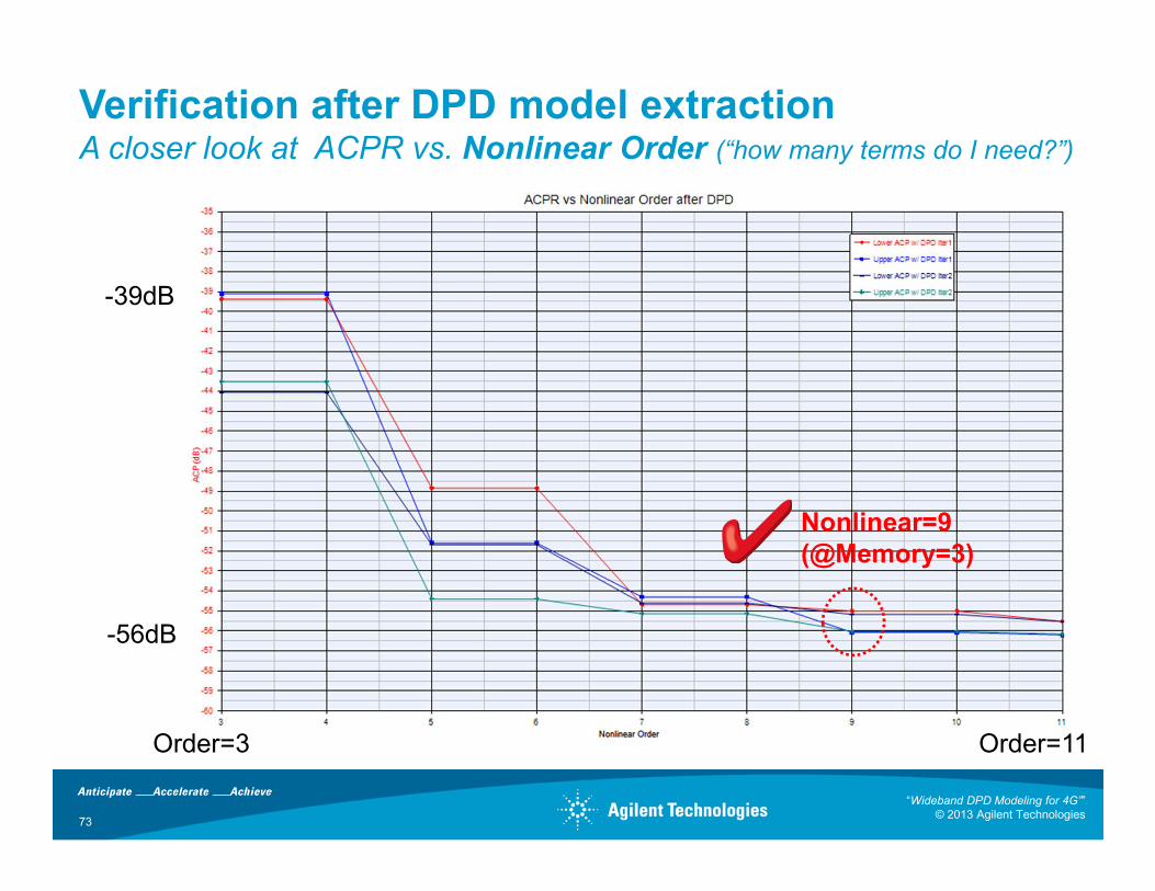
Verification after DPD model extraction A closer look at ACPR vs. Nonlinear Order (“how many terms do I need?”)
-39dB
-56dB
Order=3 Order=11
Nonlinear=9
(@Memory=3)
73
“Wideband DPD Modeling for 4G””© 2013 Agilent Technologies

Verification after DPD model extraction A closer look at ACPR vs. Memory Order (“how many terms do I need?”)
-43dB
-54dB
Memoryless Order=5
Memory=3
(@Nonlinear=7)
74
“Wideband DPD Modeling for 4G””© 2013 Agilent Technologies

Look-Up Table (LUT) DPD Algorithm Lower power, suitable for high volume (femtocell, handset PAs)
(3) Predistorters/Extractors now available in SystemVue DPD module:• Look-up Tables for Gain, Phase (does not mitigate memory FX)• Memory Polynomial • Volterra
“Wideband DPD Modeling for 4G””© 2013 Agilent Technologies
75

76
Agenda
1. Introduction and Problem Statement
2. Digital Pre-Distortion (DPD) Concepts
3. DPD verification with Agilent Hardware
4. DPD simulation with Agilent EDA Tools
5. Crest Factor Reduction (CFR)
6. Summary
“Wideband DPD Modeling for 4G””© 2013 Agilent Technologies

• Spectrally efficient wideband RF signals may have PAPR >13dB.• CFR preconditions the signal Reduce signal peaks without
significant signal distortion• CFR allows the PA to operate more efficiently – it is not a linearization
technique• CFR supplements DPD and improves DPD effectiveness• Without CFR and DPD, a basestation or handset PA must operate at
significant back-off from saturated power to maintain linearity. The back-off reduces efficiency
Benefits of CFR
1. PAs can operate closer to saturation, for improved efficiency (PAE).2. Output signal still complies with spectral mask and EVM
specifications
Crest Factor Reduction (CFR) Concepts
77
“Wideband DPD Modeling for 4G””© 2013 Agilent Technologies

78
Crest Factor Reduction (CFR) Concepts
Instantaneous PAPR
(Peak-to-Avg Power Ratio)
Psat
INPUT
POWER
OUTPUT
POWER
Pavg
Psat
INPUT
POWER
OUTPUT
POWER
Pavg
WITHOUT CFRPAPR ~13dB
Raw LTE-Advanced
WITH CFRPAPR ~7dB
Run at +6dB higher avg power
Benefit: Effectively largerRFPA with same HW BOM
“Wideband DPD Modeling for 4G””© 2013 Agilent Technologies

CFR for LTE-Advanced Downlink OFDMA
Controls EVM and band limits in the frequency domain.• Constrains constellation errors, to avoid bit errors.• Constrains the degradation on individual sub-carriers.
Allows QPSK sub-carriers to be degraded more than 64 QAM sub-carriers.Does not degrade reference signals, P-SS and S-SS.Subcarriers of out-of band are set to NULL.
79
“Wideband DPD Modeling for 4G””© 2013 Agilent Technologies

CFR for LTE-Advanced Downlink OFDMA
• No side modifications for receiver• No out-of band spectral distortion (no spectral mask measurement pass/fail issue• EVM always meets specification•Good PAR reductions•No impact of timing and frequency and channel estimation of DL
80
B u s =NO
D ata Ty pe=C o mp lex
Ma pp ing D a ta D A TA P ORT
B u s =NO
D ata Ty pe =In teg er
Q m D A TA P ORT
FFT
Freq S e que nc e=0 -po s -n eg
D ire c ti on=Inv erse
S i z e=81 92 [D FTS ize]
FFTS iz e=8 19 2 [D FTS i ze]
i fft2
0+0*j
V alu e=0 [0 +0 *j]
z e ros
G a in=1
G 3
G ai n=1
G 2
A
B loc k S iz e s =1;6 00;699 1;6 00 [[1 ,H a l f_ U s edC arriers ,D FT_z e ros ,H al f_ U s ed Carriers]]
A3
A
B loc k S iz e s =600 ;60 0 [ [H a l f_U s e dC arriers , H al f_U s ed C a rriers]]
A2
FFT
Fre qS eq uen c e =0-pos -neg
D irec tio n=Forw ard
S iz e=8 19 2 [D FTS i ze]
FFTS iz e =81 92 [D FTS ize]
fft
FFT
Freq S e que nc e=0 -po s -n eg
D ire c ti on=Inv erse
S i z e=81 92 [D FTS ize]
FFTS iz e=8 19 2 [D FTS i ze]
i fft1
MOD256
Mo du lo=256
M 1
0+0*j
V alu e=0 [0 +0*j]
DC
DPD_Ra diusClip
input out put
C lip pin gTh res ho ld=16.5e-6 [C l ip pin gThre s hold]
D P D _R ad iusClip
B u s =NO
D ata Ty pe =In teg er
S C _ S tatu s D A TAPORT
DPD
LTE_A
CFR_PostProc
out put
Qm
SC_St at us
r ef
input
E V M _Thre s h old _64 Q A M =0.06 [E V M _Th res ho ld_64QAM]
E V M_ Thres h old _1 6Q A M =0 .1 [E V M_ Th res hol d_16QAM]
E V M _Th res hol d_Q P S K =0 .12 [E V M _Thre s hold_QPSK]
O v e rs a mp l ing O p tio n=R atio 4 [O v e rs a mp l ing O p tion]
B a ndw id th=B W 2 0 M H z [B an dwidth]
D 2 D P D _L TE _A _C FR _P os tP ro c @ DPD Models
G ain =8 192 [D FTS ize]
G 1
B u s =NO
D ata Ty pe=C o mp lex
ou tpu t D A TA P ORT
“Wideband DPD Modeling for 4G””© 2013 Agilent Technologies

CFR of LTE-Advanced 20MHz Downlink
QPSK modulation, CFR algorithm set to Max EVM = 10%
81
PAPR=9dB w/o CFRPAPR=6.8dB w CFRPAPR=9dB w/o CFRPAPR=6.8dB w CFR
Spectrums with and w/o CFR
are same!
Spectrums with and w/o CFR
are same!
“Wideband DPD Modeling for 4G””© 2013 Agilent Technologies

CFR of LTE-Advanced 20MHz DownlinkAlgorithm EVM targets: QPSK < 10%, 16QAM < 8%, 64QAM < 6%
82
PAPR=8.9dB w/o CFRPAPR=7.2dB with CFRPAPR=8.9dB w/o CFRPAPR=7.2dB with CFR
ObservedEVMs w/CFR
“Wideband DPD Modeling for 4G””© 2013 Agilent Technologies

CFR of LTE-Advanced with Carrier Aggregation
83
• CFR performed separately on each Component Carrier (up to 20MHz BW)
• Component Carriers are then aggregated (summed)
CFR Approach 1 CFR Approach 2
• CC’s are carrier-aggregated (up to 100MHz BW), then CFR’d together
• Then each component carrier is re-filtered individually to remove out-of-band energy,and re-summed
“Wideband DPD Modeling for 4G””© 2013 Agilent Technologies

CFR of LTE-Advanced with Carrier AggregationApproach 1, 2x20MHz contiguous CA
84
1. Both CC0 and CC1 adopt 16-QAM and QPSK, respectively.2. CC1 magnitude threshold of polar clipping is a little larger than CC0 because
QPSK modulation can tolerate larger EVM limit, according to EVM specification.
1 1 0 1 0
DataPattern=PN9B2
1 1 0 1 0
DataPattern=PN9B3
1 1 0 1 0
DataPattern=PN9B1
1 1 0 1 0
DataPattern=PN9B4
T
SampleRate=122.9e+6Hz [SamplingRate]S1
T
SampleRate=122.9e+6Hz [SamplingRate]S2
Gain=1GainUnit=voltage
G1
Gain=1GainUnit=voltage
G2
Fc
EnvCx
Fc=2.14e+9Hz [FCarrier1]
Fc
EnvCx
Fc=2.16e+9Hz [FCarrier2]C2
UE1_Dat a
HARQ _Bit s
f r m_TD
f r m_FD
UE1_M odSymbols
U E1_ChannelBit s
LTE_A
DL
Src
CFR
NumFrames=1ClippingThreshold=13.05e-6 [ClippingThreshold2]
CFREnable=YESCRS_NumAntPorts=CRS_Tx1
NumTxAnts=Tx1UEs_RevMode=0;0;0;0;0;0 [[0,0,0,0,0,0]]
Cyc licPrefix=NormalOversamplingOption=Ratio 4 [OversamplingOption]
Bandwidth=BW 20 MHz [Bandwidth]FrameMode=FDD
ShowSystemParameters=YESLTE_DL_Src_CFR1
UE1_Dat a
HARQ _Bit s
f r m _TD
f r m _FD
UE1_ModSym bols
U E1_ChannelBit s
LTE_A
DL
Src
CFR
NumFrames=1ClippingThreshold=11.75e-6 [ClippingThreshold1]
CFREnable=YESUEs_RevMode=0;0;0;0;0;0 [[0,0,0,0,0,0]]
CyclicPrefix=NormalOversamplingOption=Ratio 4 [OversamplingOption]
Bandwidth=BW 20 MHz [Bandwidth]FrameMode=FDD
ShowSystemParameters=YESLTE_DL_Src_CFR2
FcChange
Env
CCDF
Stop=50msStart=0s
CA_CCDF
Spect rum Anal yzer
SegmentTime=50µsStart=0s
Mode=TimeGateCA_Spectrum
Component Carrier 0 (CC0)
Component Carrier 1 (CC1)
CCDF
CC1_CCDF
CCDF
CC0_CCDF1
Parameter CFREnable=YES
“Wideband DPD Modeling for 4G””© 2013 Agilent Technologies
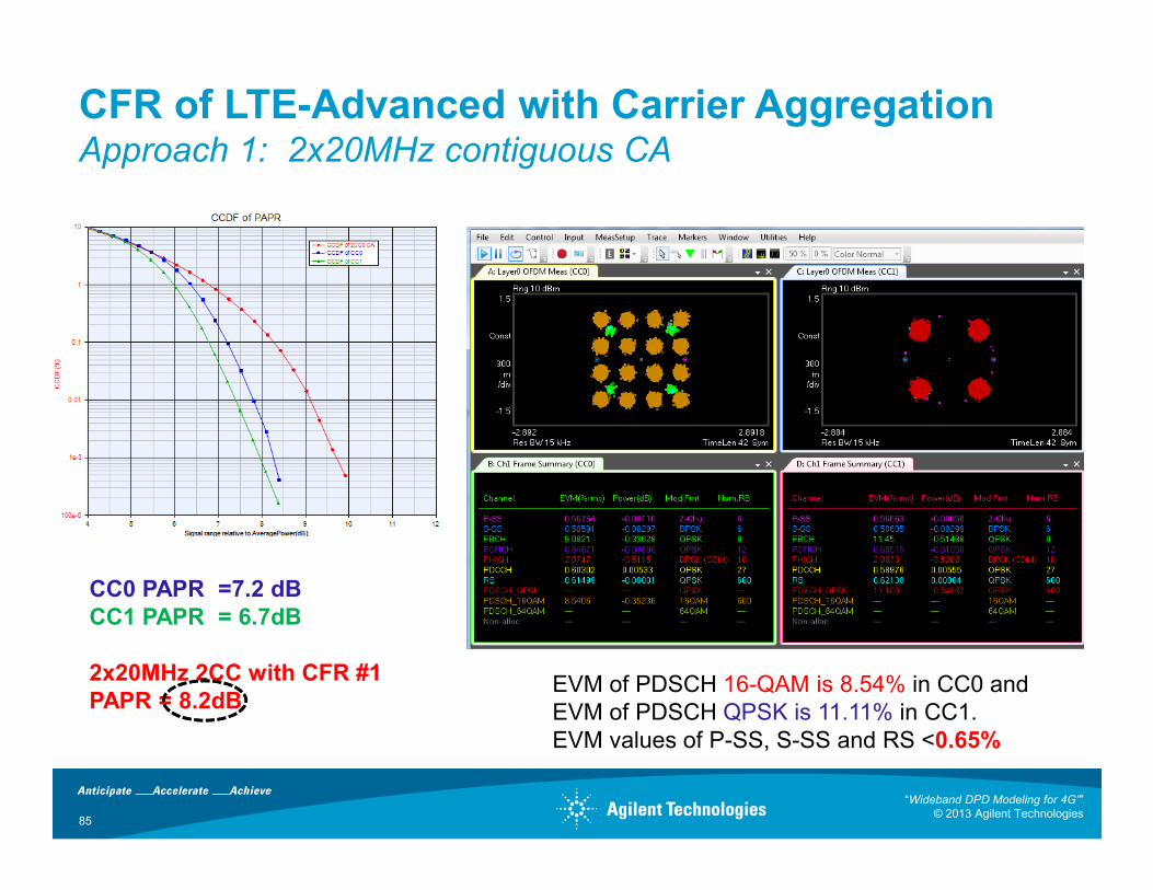
CFR of LTE-Advanced with Carrier AggregationApproach 1: 2x20MHz contiguous CA
85
EVM of PDSCH 16-QAM is 8.54% in CC0 and EVM of PDSCH QPSK is 11.11% in CC1.EVM values of P-SS, S-SS and RS <0.65%
CC0 PAPR =7.2 dB
CC1 PAPR = 6.7dB
2x20MHz 2CC with CFR #1
PAPR = 8.2dB
“Wideband DPD Modeling for 4G””© 2013 Agilent Technologies

CFR of LTE-Advanced with Carrier AggregationApproach 2: 2x20MHz contiguous CA
86
1. Both CC0 and CC1 adopt 16-QAM and QPSK, respectively.2. Aggregate CC0 and CC1 first, then do polar clipping on the
40MHz bandwidth composite CA signal.3. Each Component Carrier is filtered separately (20MHz each)4. Combine the filtered CC0 and CC1 into one CA signal again.
Parameter
CFREnable=NO
Fc
ChangeEnv
T
Sam pleRate=12 2.9 e+6Hz [SamplingRate]
S1
T
Sam pleRate=12 2.9 e+6Hz [SamplingRate]S2
Fc
EnvCx
Fc =2.16e+9Hz [FCarrier2]C2
Fc
EnvCx
Fc =2.14e+9 Hz [FCarrier1]
M ax im um Order=2057StopRipple=80
Stop Band wid th=19e6HzPas s Ripp le=0.1
Pas s Ba ndwidth=18e6Hz
FCenter=2.16e+9Hz [FCarrier2]F4
Fc
Change
Ban dwidth=0Hz
Outp utFc =2.16e+9Hz [FCarrier2]E4
Fc
Change
Bandwidth=0Hz
OutputFc =2.15e +9Hz [FCarrier]E5
Env
OutputFc=MaxA3
Fc
Change
Ban dwidth=0HzOutp utFc =2.14e+9Hz [FCarrier1]
E3
Fc
EnvCx
Fc =2.1 5e+9Hz [FCarrier]C4
T
Sam ple Rate=122 .9e +6Hz [SamplingRate]S4
Fc
CxEnv
E2
DPD_RadiusClip
in p ut o u t put
Cl ippingTh res hold=0.14250DPD_Ra diu s Clip_1
CCDF
Sto p=50ms
Start=0sCl ipp ing _CCDF
S p e c t r u m A n alyzer
Se gm entTime=50µs
Start=0sM ode=TimeGate
CA_ Spec trum _Clipping
M ax im um Order=2057StopRipple=80
Stop Band wid th=19e6HzPas s Ripp le=0.1
Pas s Ba ndwidth=18e6HzFCenter=2.14e+9Hz [FCarrier1]
F1
CCDF
Stop=50msStart=0s
CA_ CCDF
S p e c t r u m A n alyzer
Segm entTime=50µsStart=0s
M od e=TimeGateCA_ Spectrum
1 1 0 1 0
DataPatte rn=PN9
B2
1 1 0 1 0
DataPatte rn=PN9
B3
1 1 0 1 0
Data Pattern=PN9B1
1 1 0 1 0
Data Pattern=PN9B4
U E 1 _ D ata
H A R Q _ Bits
f r m_TD
f r m_FD
U E 1 _ M o d S ym bols
U E 1 _ C h a n n e lBits
LTE_A
DL
Src
CFR
Cl ip pin gThres ho ld=11.15e-6 [ClippingThreshold1]CFREnable=NO
Cy c li c Prefix=NormalOv ers am pl in gOptio n=Ratio 4 [Ov ersamplingOption]
Band wid th=BW 20 M Hz [Bandwidth]Fram eM ode=FDD
Sh owSy s te mPara meters=YESL TE_DL _Src _CFR2
U E 1 _ D ata
H A R Q _ Bits
f r m _TD
f r m _FD
U E 1 _ M o d S ym bols
U E 1 _ C h a n n e lBits
LTE_A
DL
Src
CFR
Cl ippingThres h old =12.5e-6 [Cl ippingThreshold2]CFREna ble=NO
Cy c l ic Pre fi x=NormalOv e rs a mp lingOp tion=Ratio 4 [Ov ersamplingOption]
Bandwidth=BW 2 0 M Hz [Bandwidth]Fra me Mo de=FDD
ShowSy s tem Param eters=YESLTE_DL_ Src _CFR1
Component Carrier 1 (CC1)
Component Carrier 0 (CC0)
Polar clipping
Filtering per each carrier
Combine carriers as CA signal
“Wideband DPD Modeling for 4G””© 2013 Agilent Technologies

CFR of LTE-Advanced with Carrier AggregationApproach 2: 2x20MHz contiguous CA
87
EVM of PDSCH 16-QAM is 7.80% in CC0 and EVM of PDSCH QPSK is 7.82% in CC1.All EVM values of P-SS, S-SS and RS are about 7%
2x20MHz 2CC w/o CFR
PAPR = 9 dB
2x20MHz 2CC with CFR #2
PAPR = 7.4dB
“Wideband DPD Modeling for 4G””© 2013 Agilent Technologies

Sequential Asymmetric Superposition (SAS)New CFR algorithm block in SystemVue 2013.01
Innovative elements• Asymmetric window • Adaptive window length• New scaling function • Applies to common wireless time-
domain waveforms
Results• Easy implementation• Lower spectral regrowth • Better PAPR performance• Target PAPR value is the threshold_dB value
SAS CFR
dataIn dataOut
lengthFrame=1000max_N=31
max_iter=10Beta=12.0
threshold_dB=6.0D1 DPD_SAS_CFR@DPD Models
“Wideband DPD Modeling for 4G””© 2013 Agilent Technologies
88

SAS Crest Factor Reduction exampleLTE-A 2CC Carrier Aggregation
CFR for 3GPP LTE-A DL Carrier Aggregation Waveform
Component Carrier 0 (CC0)
Component Carrier 1 (CC1)
T
Sam pleRate=1 22.9e +6Hz [Sam pl ingRate]S1
Gain=1
GainUni t=v oltageG1
Env
Fc
EnvCx
Fc =2.14e+9 Hz [FCarrier1]
CCDF
Stop=100ms
Start=0s
CC0_CCDF
1 1 0 1 0
DataPattern =PN9
B4
1 1 0 1 0
DataPattern =PN9
B1
1 1 0 1 0
DataPattern=PN9B2
1 1 0 1 0
DataPattern=PN9
B3
T
Sam pleRate=1 22.9e +6Hz [Sam pl ingRate]
S2
Gain=1
GainUni t=v ol tage
G2
Fc
EnvCx
Fc =2.1 6e+9Hz [FCarrier2]
C2
CCDF
Stop=1 00ms
Start=0sCC1_CCDF
U E 1 _ D ata
H A R Q _ B its
f r m _TD
f r m _FD
U E 1 _ M o d S y m bols
U E 1 _ C h a n n e lB its
LTE_A
DL
Src
CFR
Av oidPhas e Dis c o ntinuity=NO
ClippingThres hold=13.15e-6
CFREn able=NO
Num Fram es=1
UEs _n_ RNTI=(1x 6) [1,2,3 ,4,5,6]
UEs _Spe c ific RS=(1x 6) [0,0,0,0,0,0]UEs _Tran s M od e=(1x 6) [0,0,0,0,0,0]
Cy c l i c Prefi x =Normal
Ov ers am plingOption=Ratio 4
Ban dwidth=BW 20 M Hz [Ban dwidth]
Fram eM ode=FDDShowSy s tem Param eters=YES
LTE_DL_Src _CFR2
U E 1 _ D ata
H A R Q _ B its
f r m _TD
f r m _FD
U E 1 _ M o d S y m bols
U E 1 _ C h a n n e lB its
LTE_A
DL
Src
CFR
Av oidPhas e Dis c o ntinuity=NOClippingThres hold=13.15e-6
CFREn able=NO
Num Fram es=1
UEs _n_ RNTI=(1x 6) [1,2,3 ,4,5,6]
UEs _Spe c ific RS=(1x 6) [0,0,0,0,0,0]
UEs _Tran s M od e=(1x 6) [0,0,0,0,0,0]Cy c l i c Prefi x =Normal
Ov ers am plingOption=Ratio 4
Ban dwidth=BW 20 M Hz [Ban dwidth]
Fram eM ode=FDD
ShowSy s tem Param eters=YES
LTE_DL_Src _CFR1
Fc
CxEnv
E2
DPD_ SAS_CFR
length Fram e=3000
m ax _N=51
m ax _i ter=10Beta=12.0
thres hold_dB=6.0
D1
Fc
EnvCx
Fc =2 .15e+9Hz [FCarrier]
C4
CCDF
Stop=50ms
Start=0s
CFR_CA_CCDF
Spect rum Anal yzer
Seg m entTim e=50µs
Start=0s
M ode=Tim eGate
CA_ Spec trum _CFR
SAS CFR block
“Wideband DPD Modeling for 4G””© 2013 Agilent Technologies
89

SAS Crest Factor Reduction exampleLTE-A 2CC Carrier Aggregation
“Wideband DPD Modeling for 4G””© 2013 Agilent Technologies
90

SAS Crest Factor Reduction exampleMulti-Standard Radio (MSR)
GSM
WCDMA
LTE
GSM
CFR algorithm suitable for Multi-format, Multi-band, and Instrument waveforms
“Wideband DPD Modeling for 4G””© 2013 Agilent Technologies
91

92
Agenda
1. Introduction and Problem Statement
2. Digital Pre-Distortion (DPD) Concepts
3. DPD verification with Agilent Hardware
4. DPD simulation with Agilent EDA Tools
5. Crest Factor Reduction (CFR)
6. Summary
“Wideband DPD Modeling for 4G””© 2013 Agilent Technologies

Problem statement
Modern communication systems try to meet conflicting requirements:• Signals with high PAPR, that then require inefficient back-off • RF PAs with high PAE, that then cause time & freq distortions
Solution approaches
• Digital Pre-Distortion (DPD) and Crest Factor Reduction (CFR) algorithms together help overcome conflicting requirements.
• SystemVue offers a practical DPD modeling flow • Connects to/from open, enterprise modeling & EDA tools• Control your own IP, or leverage Agilent’s IP to model any HW or
Algorithms you don’t have access to• Re-use commonly available test equipment• Create virtual systems using simulators, test equip, scripting, UI
Summary
93
“Wideband DPD Modeling for 4G””© 2013 Agilent Technologies

Generalized Wireless Transmitter Path
BB PHY
CFR DPDUp
convertPA
EnvTracking
DAC
Downconvert
ADCAdapt
Duplexer
• Model any blocks not included with your final product, and get on with your project• Imitate/Model key missing pieces of IP and hardware, and maintain control• Verify against realistic system specifications, which may be controlled externally
94
“Wideband DPD Modeling for 4G””© 2013 Agilent Technologies

95
Questions & Answers
“Wideband DPD Modeling for 4G””© 2013 Agilent Technologies

Agilent LTE/LTE-Advanced textbookDiscusses many of the concepts shown today
96
“Wideband DPD Modeling for 4G””© 2013 Agilent Technologies
NEW FOR 2013SystemVue applications featured in this book• LTE-Advanced (3GPP Releases 8-12)• MIMO channel/Over-the-Air testing• Multi-Standard Radio (MSR)• DPD, Crest Factor Reduction• Integration of Design & Test
http://www.agilent.com/find/LTEbook
ISBN 978-1-1199-6257-1 (Wiley & Sons)

“Novel Wideband DPD Modeling Platform for 4G”
97
THANK YOU
W1716 Digital Pre-DistortionWeb - www.agilent.com/find/eesof-systemvue-dpd-builderApp Note - http://cp.literature.agilent.com/litweb/pdf/5990-6534EN.pdfApp Note - http://cp.literature.agilent.com/litweb/pdf/5990-7818EN.pdfApp Note - http://cp.literature.agilent.com/litweb/pdf/5990-8883EN.pdf
SystemVuewww.agilent.com/find/eesof-systemvue www.agilent.com/find/eesof-systemvue-videoswww.agilent.com/find/eesof-systemvue-evaluation
Or, contact your regional Agilent resourcewww.agilent.com/find/eesof-contact
“Wideband DPD Modeling for 4G””© 2013 Agilent Technologies