Embed Size (px)
Citation preview
IC yield estimation at early stages of the design cycle
Tom Chena,* , Von-Kyoung Kimb, Mick Tegethoff1
aDepartment of Electrical Engineering, Colorado State University, Fort Collins, CO 80523, USAbSun Microsystems, 901 San Antonio Rd., MS USUN02-302, Palo Alto, CA 94303 USA
Accepted 20 November 1998
Abstract
A yield prediction in the early stage of the design cycle can give positive impacts on cost and quality of IC manufacturing. However, thelack of prediction tool, that do not rely on layout data, makes it difficult to estimate the chip yield in the early design phase. This articledescribes yield prediction models for random logic and SRAM blocks using inductive fault analysis. The proposed model predicts defectsensitive area early in the design cycle as a function of simple circuit parameters without using any layout data. We applied both models tocommercial ASIC products for validation. The IC yield estimation using the sensitive area model showed an acceptable accuracy of a wellbelow 10% error.q 1999 Elsevier Science Ltd. All rights reserved.
Keywords:Yield estimation; Yield prediction; Standard cell design; Early yield estimation; SRAM; Yield model; Sensitive area; Inductive fault analysis(IFA)
1. Introduction
Manufacturing yield is one of the key parameters used todetermine overall manufacturing cost. It is also used for testplanning and determining manufacturing test cost. Withincreasing IC complexity and ever tight time-to-marketrequirement, it is highly desirable that test planning andestimation of manufacturing test cost and other costs relatedto manufacturing are carried out at early stages of the designcycle. Therefore, it is important to be able to estimate manu-facturing yield at early design stages of the design cyclewhere layout and even the complete netlist data are notavailable.
Cunningham [1] summarized popular IC yield models.Popular yield models include Poisson model [2], Murphymodel [3], Seeds model [4], Moore model [5], Price model[6], Dingwall model [7] and negative binomial model [8,9]Table 1 summarizes the popular chip yield models, in whichY is the manufacturing IC yield,D0 is the process defectdensity,A is the chip area, anda is usually referred to asclustering parameter, which increases with decreasingvariance (s 2) in the distribution of defects.D0A is theaverage number of defects per chip for the given defectdensityD0 and the chip areaA. The accuracy of chip yield
estimation mainly depends on the estimation accuracy of thechip area since the defect density information is usuallydetermined by the fabrication line defect statistics. Moredetailed discussions in IC yield models can be found in [1].
Many studies related to the estimation of IC yield werecarried out. Inductive fault analysis(IFA) [10-12], and ICyield estimation using critical area extraction [13-17] wereproposed. IFA is a systematic approach to determine whichdefects are more likely to occur in a given IC layout. Realis-tic faults and their sensitive areas are extracted from circuitlayouts. The faults are ranked and their probabilities arereported based on the extracted sensitive areas.
Sensitive area is an area of layout sensitive to spotdefects. A chip with large sensitive area indicates that thechip has a high probability of having defects during ICmanufacturing. Therefore, the larger the sensitive area, thelower the chip yield will be. Walker [13] and Wagner et al.,[17] developed CAD tools which estimate the IC yield usingsensitive area extracted from layout. Their results showedpossibility of estimating IC yield before actual fabrication.However, the sensitive area extraction from the layout isusually very CPU-intensive. Moreover, sensitive areaextraction requires chip layout to predict the IC yield.Therefore, it is difficult to predict the chip yield in anearly stage of the design cycle.
A few recent studies were presented in the area of ICmanufacturability analysis [18,19], and early IC yield fore-casting [20,21]. In [18], critical area of various layers wasextracted from GDS layout using a commercial layout
Microelectronics Journal 30 (1999) 725–732
MicroelectronicsJournal
MEJ 545
0026-2692/99/$ - see front matterq 1999 Elsevier Science Ltd. All rights reserved.PII: S0026-2692(98)00158-X
* Corresponding author. Tel.: 001 970 4916574; fax: 001 970 491-2249.E-mail addresses:[email protected] (T. Chen), [email protected]
(V.-K. Kim)1 M. Tegethoff is with Celestica, CO.
extraction tool. Structural information and statisticalinformation of the given circuit were also collected fromthe circuit netlist. Then, different design environments canbe analyzed based on the extracted circuit information.However, the detailed circuit information is usually notavailable in the early design. Thus, a new IC yield forecast-ing model for submicron ICs was developed [20,21]. Theyield model was derived from Poisson model using criticalarea approximation. It was designed to forecast IC yieldwithout detailed circuit information for early IC yieldprediction. Also, Maly et al. [19] explored several importantdesign-for-manufacturability (DFM) issues.
Domer et al. [22] proposed a different approach to predictchip yield. Their proposed model estimates cost and yield offinal product based on manufacturing data. Their model isderived from the empirical test data. Their yield estimationmodel supports three types of circuit, memory blocks,random logic blocks, and IO blocks. Alayout sensitivity2was introduced to scale the defect sensitivity for differentcircuit types. The layout sensitivity values for memory,random logic, and IO circuits were set to 0.8, 0.5, and0.25, respectively, according to their experiments. A sensi-tive area of a given block is defined as the product of totallayout area of the block times the corresponding layoutsensitivity value. Their yield model requires chip layoutarea which makes it difficult to predict the chip yield in anearly stage of the design cycle.
In this article, we propose IC yield prediction models formemory circuits and for random logic circuits implemented
using the standard cell design approach. Our yieldprediction model was developed based on a sensitive areaestimation which is similar to Domer et al.’s approach.However, we use IFA to extract the sensitive areas from aset of benchmark circuit layouts and fit them with a moreaccurate analytical model based on a set of circuit para-meters, such as the number of logic gates and logic netsinstead of using empirical data. Therefore, the proposedsensitive area model can predict the chip yield withoutchip layouts.
The sensitive area prediction model was applied to acommercial ASIC product for validation. Yield predictionon the ASIC part shows about 5% to 6% errors dependingupon IC yield formula used in prediction. Since the yieldprediction was made based on circuit parameters rather thanlayout, we believe the model can be used as a first orderapproximation in the early stage of the design cycle.
The remaining sections of this article are organized asfollows: Section 2 discusses the proposed sensitive areamodel in detail. Section 2.1 describes model parameterselection. Section 2.2 shows the defect distribution andthe sensitive area extraction using IFA. Sections 2.3 and2.4 discuss the sensitive area prediction model for randomlogic and SRAM. Section 3 shows examples of model appli-cations to commercial ASIC products. Finally, Section 4concludes the article.
2. Sensitive area estimation model
The total sensitive area (TSA) is the integration of thesensitive areas for all possible defects. The average numberof defects(D0A) is calculated by the estimated TSA times thegiven defect density. The defect density is given by thefabrication data. A chip yield is predicted by putting theaverage number of defects into an IC yield model.
The process of building the sensitive area predictionmodel is as follows: First, benchmark circuit layouts weregenerated by a commercial semi-custom layout synthesistool. Table 2 shows the characteristics of the benchmarkcircuits used and their layout areas. Second, the sensitive
T. Chen et al. / Microelectronics Journal 30 (1999) 725–732726
Table 1IC Yield Models
Name Model
Poisson [2] Y� e2D0A
Murphy [3] Y � �1 2 e2D0A=D0A�2
Seeds [4] Y � 1=1 1 D0AMoore [5] Y � e2
����D0Ap
Price [6] Y � prodni�1�1=1 1 DiA�
Dingwall [7] Y � �1 1 D0A=3�23
Neg. bin [8,9] Y � �1 1 D0A=a�2a
Table 2Characteristics of ISCAS Benchmark Circuits
Circuit Gate Net IO Area [mm2]
C17 6 22 7 1786C432 14 247 43 629498C499 163 297 73 1062328C880 247 429 86 1126230C1355 293 459 73 1854306C1908 202 342 58 1735008C2670 442 863 221 3997970C3540 889 1182 72 5365318C5315 978 1673 301 11031048C6288 825 1181 64 8796370C7552 1353 2105 313 14166761
Table 3Defect size distribution and frequency of occurrence
size m1lp m2lp m3lp m5lp plp c1lp c2lp sum
1 13 6 0 0 6 1 0 262 20 22 0 0 7 3 0 523 13 9 1 0 3 0 1 274 4 2 0 0 0 0 1 75 4 2 2 1 1 0 1 116 2 4 2 2 0 0 0 107 0 2 0 0 1 0 0 38 1 2 1 0 0 0 0 49 1 2 1 0 0 0 0 410 0 0 1 0 0 0 0 1total 58 51 8 3 18 4 3 145
areas were extracted using IFA with the defect statisticsfrom a commercial 0.5mm CMOS process. Third, theextracted sensitive areas were used to select the optimumpredictor through sensitivity analysis. Fourth, curve-fittingprocesses were performed to build the model. Half of thebenchmark circuits were used to build the model and theother remaining half were used to validate the model.Finally, the sensitive area prediction model was obtained.
The sensitive area model for random logic is a function ofbasic circuit parameters in order to achieve an earlyprediction without knowing detailed netlist or chip layoutinformation.
2.1. Model parameter selection
The proposed sensitive area model for random logic is
T. Chen et al. / Microelectronics Journal 30 (1999) 725–732 727
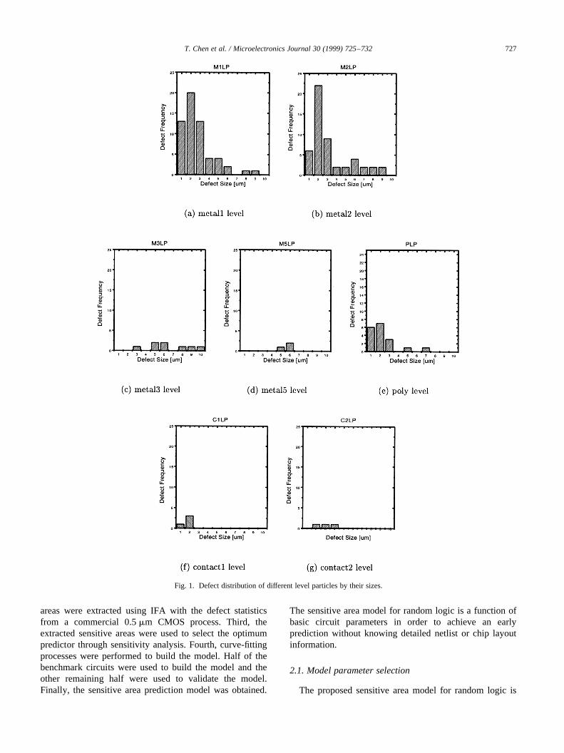
Fig. 1. Defect distribution of different level particles by their sizes.
based on standard cell designs. The potential parameters ofthe TSA model may include:
• Number of gates (referenced structures, represents totalnumber of gates),
• Number of nets (including internal nets, input pins, andoutput pins),
• Gate ratio (gates divided by area),• Logic depth (the longest logic path from an input to an
output),• Cell size (transistor feature width),• Routing ratio (routing area as a percentage of the total
block chip area),• Average fan-ins/fan-outs.
To determine which parameters should be used for sensi-tive area prediction, sensitivity analyses were performed foreach potential parameter against the ISCAS circuits andtheir layouts. The experiments showed that the number ofgates (G) and the number of nets (N) inside the circuit weredetermined as the most sensitive parameters for the TSA.Other parameters do not have as significant impact on sensi-tive area as the number of gates and nets. For example,number of IO ports are included in the total number ofnets. Therefore, the sensitive area prediction model is deter-mined as a function of the two circuit parameters,G and N.
2.2. Sensitive area extraction
The ISCAS benchmark circuits were used to develop andevaluate the sensitive area model for random logic withstandard-cell style layout. The sensitive areas wereextracted using IFA, which takes the defect spectrum offabrication line as an input, and reports the sensitive areaas an output. In CMOS IC manufacturing, a particle cancause bridging faults, breaking faults, and transistor stuckfaults depending upon the characteristics of particles caus-ing the defect. One such characteristics is the size of theparticles. Defect type and size distributions are importantparameters to determine the sensitive area. Our model isbased on a commercial fabrication line defect distributiondata from a 0.5mm five-metal single-poly, CMOS process.We will refer to this process as ‘process A’ throughout thearticle.
Table 3 shows the defect size distribution and thefrequency of occurrence for process A. A total of 162defects are collected to analyze the size distribution. Thefirst column is the defect size from 1 to 10mm, and thesecond to the eighth columns show the frequency of differ-ent types of defects occurring at different sizes. M1LPdenotes metal1 level particle (often causing metal1 tometal1 shorts), PLP denotes poly level particle, and C1LPdenotes contact1 level particle (poly to metal1 shorts).M1LP through PLP are intra-layer particles while C1LPand C2LP are inter-layer particles, denoting poly tometal1 shorts (C1LP) and metal1 to metal2 shorts (C2LP).About 90% of the defects are identified, while defects largerthan 10mm are excluded to simplify the analysis.
Fig. 1 shows the defect distribution by particle levels.Most of the defects are intra-layer, conductive particles,mainly metal1, metal2, and poly while inter-layer particlessuch as contact1 and contact2 are relatively rare. Accordingto this result, one can imply that the probability of bridgefaults is much higher than that of break faults.
IFA simulations based on the defect distributiondescribed earlier were performed for different defect sizes.The result is shown in Table 4. The sensitive area extraction
T. Chen et al. / Microelectronics Journal 30 (1999) 725–732728
Table 4Sensitive area extraction results
Circuit Defect size [mm] TSA
1 2 3 4 5 6 7 8 9 [mm2]C17 1078 4537 3122 1170 1199 1468 588 972 1100 15234C432 45171 160008 94379 30962 28736 31789 11715 18118 19287 440165C499 74418 258348 153264 50302 46808 51745 18980 29317 29852 713034C880 83223 287951 169194 55477 51387 56255 20502 31771 33670 789430C1355 126244 454998 270175 88871 82306 89329 32094 49659 52250 1245926C1908 125931 437834 256137 83399 77048 83560 30193 46817 49447 1190366C2670 269943 950057 563194 183921 169811 183899 66215 102015 97143 2586198C3540 376951 1323595 781566 254134 234100 252037 90096 138824 90096 3541399C5315 751959 2641191 1568970 511927 471923 508002 182419 279147 278914 7194452C6288 620415 2218020 1302390 420583 1302390 409641 146067 224381 234619 6878506C7552 982320 3397634 2005184 652057 601608 649013 232635 356172 367615 9244238
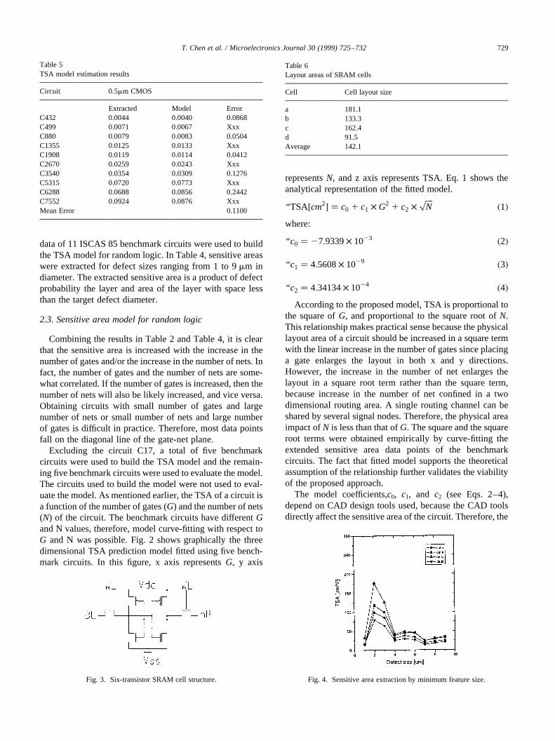
Fig. 2. Sensitive area model for random logic.
data of 11 ISCAS 85 benchmark circuits were used to buildthe TSA model for random logic. In Table 4, sensitive areaswere extracted for defect sizes ranging from 1 to 9mm indiameter. The extracted sensitive area is a product of defectprobability the layer and area of the layer with space lessthan the target defect diameter.
2.3. Sensitive area model for random logic
Combining the results in Table 2 and Table 4, it is clearthat the sensitive area is increased with the increase in thenumber of gates and/or the increase in the number of nets. Infact, the number of gates and the number of nets are some-what correlated. If the number of gates is increased, then thenumber of nets will also be likely increased, and vice versa.Obtaining circuits with small number of gates and largenumber of nets or small number of nets and large numberof gates is difficult in practice. Therefore, most data pointsfall on the diagonal line of the gate-net plane.
Excluding the circuit C17, a total of five benchmarkcircuits were used to build the TSA model and the remain-ing five benchmark circuits were used to evaluate the model.The circuits used to build the model were not used to eval-uate the model. As mentioned earlier, the TSA of a circuit isa function of the number of gates (G) and the number of nets(N) of the circuit. The benchmark circuits have differentGand N values, therefore, model curve-fitting with respect toG and N was possible. Fig. 2 shows graphically the threedimensional TSA prediction model fitted using five bench-mark circuits. In this figure, x axis representsG, y axis
representsN, and z axis represents TSA. Eq. 1 shows theanalytical representation of the fitted model.
“ TSA�cm2� � c0 1 c1 × G2 1 c2 ×���Np �1�
where:
“c 0 � 27:9339× 1023 �2�
“c 1 � 4:5608× 1029 �3�
“c 2 � 4:34134× 1024 �4�According to the proposed model, TSA is proportional to
the square ofG, and proportional to the square root ofN.This relationship makes practical sense because the physicallayout area of a circuit should be increased in a square termwith the linear increase in the number of gates since placinga gate enlarges the layout in both x and y directions.However, the increase in the number of net enlarges thelayout in a square root term rather than the square term,because increase in the number of net confined in a twodimensional routing area. A single routing channel can beshared by several signal nodes. Therefore, the physical areaimpact ofN is less than that ofG. The square and the squareroot terms were obtained empirically by curve-fitting theextended sensitive area data points of the benchmarkcircuits. The fact that fitted model supports the theoreticalassumption of the relationship further validates the viabilityof the proposed approach.
The model coefficients,c0, c1, and c2 (see Eqs. 2–4),depend on CAD design tools used, because the CAD toolsdirectly affect the sensitive area of the circuit. Therefore, the
T. Chen et al. / Microelectronics Journal 30 (1999) 725–732 729
Table 5TSA model estimation results
Circuit 0.5mm CMOS
Extracted Model ErrorC432 0.0044 0.0040 0.0868C499 0.0071 0.0067 XxxC880 0.0079 0.0083 0.0504C1355 0.0125 0.0133 XxxC1908 0.0119 0.0114 0.0412C2670 0.0259 0.0243 XxxC3540 0.0354 0.0309 0.1276C5315 0.0720 0.0773 XxxC6288 0.0688 0.0856 0.2442C7552 0.0924 0.0876 XxxMean Error 0.1100
Table 6Layout areas of SRAM cells
Cell Cell layout size
a 181.1b 133.3c 162.4d 91.5Average 142.1
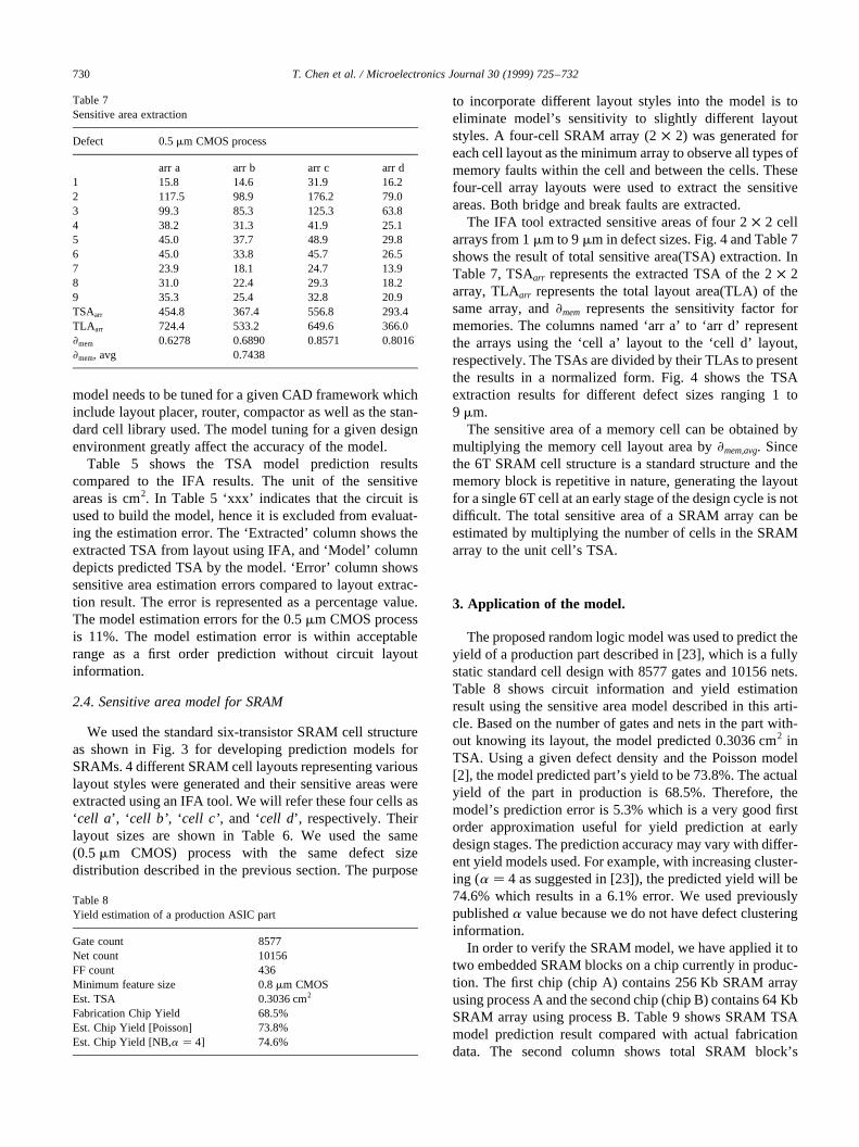
Fig. 3. Six-transistor SRAM cell structure. Fig. 4. Sensitive area extraction by minimum feature size.
model needs to be tuned for a given CAD framework whichinclude layout placer, router, compactor as well as the stan-dard cell library used. The model tuning for a given designenvironment greatly affect the accuracy of the model.
Table 5 shows the TSA model prediction resultscompared to the IFA results. The unit of the sensitiveareas is cm2. In Table 5 ‘xxx’ indicates that the circuit isused to build the model, hence it is excluded from evaluat-ing the estimation error. The ‘Extracted’ column shows theextracted TSA from layout using IFA, and ‘Model’ columndepicts predicted TSA by the model. ‘Error’ column showssensitive area estimation errors compared to layout extrac-tion result. The error is represented as a percentage value.The model estimation errors for the 0.5mm CMOS processis 11%. The model estimation error is within acceptablerange as a first order prediction without circuit layoutinformation.
2.4. Sensitive area model for SRAM
We used the standard six-transistor SRAM cell structureas shown in Fig. 3 for developing prediction models forSRAMs. 4 different SRAM cell layouts representing variouslayout styles were generated and their sensitive areas wereextracted using an IFA tool. We will refer these four cells as‘cell a’, ‘ cell b’, ‘cell c’, and ‘cell d’, respectively. Theirlayout sizes are shown in Table 6. We used the same(0.5mm CMOS) process with the same defect sizedistribution described in the previous section. The purpose
to incorporate different layout styles into the model is toeliminate model’s sensitivity to slightly different layoutstyles. A four-cell SRAM array (2× 2) was generated foreach cell layout as the minimum array to observe all types ofmemory faults within the cell and between the cells. Thesefour-cell array layouts were used to extract the sensitiveareas. Both bridge and break faults are extracted.
The IFA tool extracted sensitive areas of four 2× 2 cellarrays from 1mm to 9mm in defect sizes. Fig. 4 and Table 7shows the result of total sensitive area(TSA) extraction. InTable 7, TSAarr represents the extracted TSA of the 2× 2array, TLAarr represents the total layout area(TLA) of thesame array, and2mem represents the sensitivity factor formemories. The columns named ‘arr a’ to ‘arr d’ representthe arrays using the ‘cell a’ layout to the ‘cell d’ layout,respectively. The TSAs are divided by their TLAs to presentthe results in a normalized form. Fig. 4 shows the TSAextraction results for different defect sizes ranging 1 to9 mm.
The sensitive area of a memory cell can be obtained bymultiplying the memory cell layout area by2mem,avg. Sincethe 6T SRAM cell structure is a standard structure and thememory block is repetitive in nature, generating the layoutfor a single 6T cell at an early stage of the design cycle is notdifficult. The total sensitive area of a SRAM array can beestimated by multiplying the number of cells in the SRAMarray to the unit cell’s TSA.
3. Application of the model.
The proposed random logic model was used to predict theyield of a production part described in [23], which is a fullystatic standard cell design with 8577 gates and 10156 nets.Table 8 shows circuit information and yield estimationresult using the sensitive area model described in this arti-cle. Based on the number of gates and nets in the part with-out knowing its layout, the model predicted 0.3036 cm2 inTSA. Using a given defect density and the Poisson model[2], the model predicted part’s yield to be 73.8%. The actualyield of the part in production is 68.5%. Therefore, themodel’s prediction error is 5.3% which is a very good firstorder approximation useful for yield prediction at earlydesign stages. The prediction accuracy may vary with differ-ent yield models used. For example, with increasing cluster-ing (a � 4 as suggested in [23]), the predicted yield will be74.6% which results in a 6.1% error. We used previouslypublisheda value because we do not have defect clusteringinformation.
In order to verify the SRAM model, we have applied it totwo embedded SRAM blocks on a chip currently in produc-tion. The first chip (chip A) contains 256 Kb SRAM arrayusing process A and the second chip (chip B) contains 64 KbSRAM array using process B. Table 9 shows SRAM TSAmodel prediction result compared with actual fabricationdata. The second column shows total SRAM block’s
T. Chen et al. / Microelectronics Journal 30 (1999) 725–732730
Table 7Sensitive area extraction
Defect 0.5mm CMOS process
arr a arr b arr c arr d1 15.8 14.6 31.9 16.22 117.5 98.9 176.2 79.03 99.3 85.3 125.3 63.84 38.2 31.3 41.9 25.15 45.0 37.7 48.9 29.86 45.0 33.8 45.7 26.57 23.9 18.1 24.7 13.98 31.0 22.4 29.3 18.29 35.3 25.4 32.8 20.9TSAarr 454.8 367.4 556.8 293.4TLAarr 724.4 533.2 649.6 366.02mem 0.6278 0.6890 0.8571 0.80162mem, avg 0.7438
Table 8Yield estimation of a production ASIC part
Gate count 8577Net count 10156FF count 436Minimum feature size 0.8mm CMOSEst. TSA 0.3036 cm2
Fabrication Chip Yield 68.5%Est. Chip Yield [Poisson] 73.8%Est. Chip Yield [NB,a � 4] 74.6%
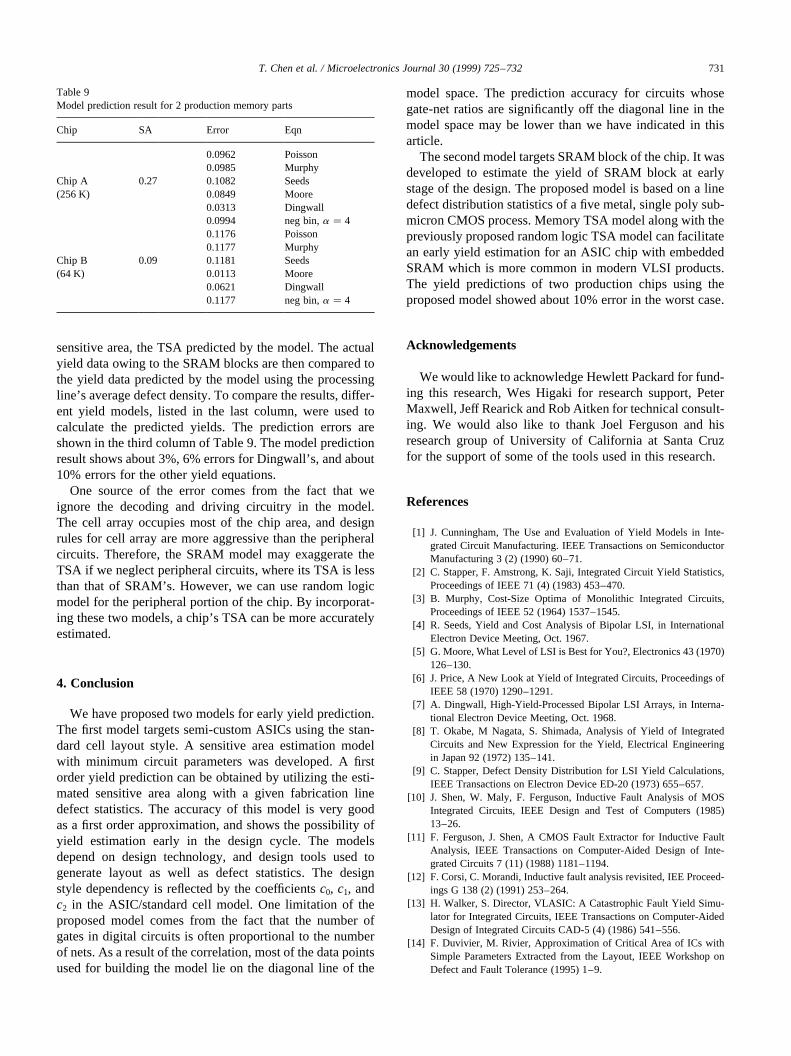
sensitive area, the TSA predicted by the model. The actualyield data owing to the SRAM blocks are then compared tothe yield data predicted by the model using the processingline’s average defect density. To compare the results, differ-ent yield models, listed in the last column, were used tocalculate the predicted yields. The prediction errors areshown in the third column of Table 9. The model predictionresult shows about 3%, 6% errors for Dingwall’s, and about10% errors for the other yield equations.
One source of the error comes from the fact that weignore the decoding and driving circuitry in the model.The cell array occupies most of the chip area, and designrules for cell array are more aggressive than the peripheralcircuits. Therefore, the SRAM model may exaggerate theTSA if we neglect peripheral circuits, where its TSA is lessthan that of SRAM’s. However, we can use random logicmodel for the peripheral portion of the chip. By incorporat-ing these two models, a chip’s TSA can be more accuratelyestimated.
4. Conclusion
We have proposed two models for early yield prediction.The first model targets semi-custom ASICs using the stan-dard cell layout style. A sensitive area estimation modelwith minimum circuit parameters was developed. A firstorder yield prediction can be obtained by utilizing the esti-mated sensitive area along with a given fabrication linedefect statistics. The accuracy of this model is very goodas a first order approximation, and shows the possibility ofyield estimation early in the design cycle. The modelsdepend on design technology, and design tools used togenerate layout as well as defect statistics. The designstyle dependency is reflected by the coefficientsc0, c1, andc2 in the ASIC/standard cell model. One limitation of theproposed model comes from the fact that the number ofgates in digital circuits is often proportional to the numberof nets. As a result of the correlation, most of the data pointsused for building the model lie on the diagonal line of the
model space. The prediction accuracy for circuits whosegate-net ratios are significantly off the diagonal line in themodel space may be lower than we have indicated in thisarticle.
The second model targets SRAM block of the chip. It wasdeveloped to estimate the yield of SRAM block at earlystage of the design. The proposed model is based on a linedefect distribution statistics of a five metal, single poly sub-micron CMOS process. Memory TSA model along with thepreviously proposed random logic TSA model can facilitatean early yield estimation for an ASIC chip with embeddedSRAM which is more common in modern VLSI products.The yield predictions of two production chips using theproposed model showed about 10% error in the worst case.
Acknowledgements
We would like to acknowledge Hewlett Packard for fund-ing this research, Wes Higaki for research support, PeterMaxwell, Jeff Rearick and Rob Aitken for technical consult-ing. We would also like to thank Joel Ferguson and hisresearch group of University of California at Santa Cruzfor the support of some of the tools used in this research.
References
[1] J. Cunningham, The Use and Evaluation of Yield Models in Inte-grated Circuit Manufacturing. IEEE Transactions on SemiconductorManufacturing 3 (2) (1990) 60–71.
[2] C. Stapper, F. Amstrong, K. Saji, Integrated Circuit Yield Statistics,Proceedings of IEEE 71 (4) (1983) 453–470.
[3] B. Murphy, Cost-Size Optima of Monolithic Integrated Circuits,Proceedings of IEEE 52 (1964) 1537–1545.
[4] R. Seeds, Yield and Cost Analysis of Bipolar LSI, in InternationalElectron Device Meeting, Oct. 1967.
[5] G. Moore, What Level of LSI is Best for You?, Electronics 43 (1970)126–130.
[6] J. Price, A New Look at Yield of Integrated Circuits, Proceedings ofIEEE 58 (1970) 1290–1291.
[7] A. Dingwall, High-Yield-Processed Bipolar LSI Arrays, in Interna-tional Electron Device Meeting, Oct. 1968.
[8] T. Okabe, M Nagata, S. Shimada, Analysis of Yield of IntegratedCircuits and New Expression for the Yield, Electrical Engineeringin Japan 92 (1972) 135–141.
[9] C. Stapper, Defect Density Distribution for LSI Yield Calculations,IEEE Transactions on Electron Device ED-20 (1973) 655–657.
[10] J. Shen, W. Maly, F. Ferguson, Inductive Fault Analysis of MOSIntegrated Circuits, IEEE Design and Test of Computers (1985)13–26.
[11] F. Ferguson, J. Shen, A CMOS Fault Extractor for Inductive FaultAnalysis, IEEE Transactions on Computer-Aided Design of Inte-grated Circuits 7 (11) (1988) 1181–1194.
[12] F. Corsi, C. Morandi, Inductive fault analysis revisited, IEE Proceed-ings G 138 (2) (1991) 253–264.
[13] H. Walker, S. Director, VLASIC: A Catastrophic Fault Yield Simu-lator for Integrated Circuits, IEEE Transactions on Computer-AidedDesign of Integrated Circuits CAD-5 (4) (1986) 541–556.
[14] F. Duvivier, M. Rivier, Approximation of Critical Area of ICs withSimple Parameters Extracted from the Layout, IEEE Workshop onDefect and Fault Tolerance (1995) 1–9.
T. Chen et al. / Microelectronics Journal 30 (1999) 725–732 731
Table 9Model prediction result for 2 production memory parts
Chip SA Error Eqn
0.0962 Poisson0.0985 Murphy
Chip A 0.27 0.1082 Seeds(256 K) 0.0849 Moore
0.0313 Dingwall0.0994 neg bin,a � 40.1176 Poisson0.1177 Murphy
Chip B 0.09 0.1181 Seeds(64 K) 0.0113 Moore
0.0621 Dingwall0.1177 neg bin,a � 4
[15] I. Bubel et al. AFFCCA:A Tool for Critical Area Analysis with Circu-lar Defects and Lithography Deformed Layout, in IEEE Workshop onDefect and Fault Tolerance, (1995) 10–18.
[16] G. Allan, A. Walton, Hirarchical Critical Area Extraction with the EYETool, in IEEE Workshop on Defect and Fault Tolerance (1995) 28–36.
[17] I. Wagner, I. Koren, An Interactive VLSI CAD Tool for Yield Esti-mation, IEEE Transactions on Semiconductor Manufacturing 8 (2)(1995) 130–138.
[18] H. Heineken, W. Maly, Manufacturability Analysis EnvironmentMAPEX, in Custom Integrated Circuit Conference (1994) 309–312.
[19] W. Maly et al., Design for Manufacturability in the Submicron Domain,International Conference on Computer-Aided Design (1996) 690–697.
[20] W. Maly, H. Heineken, F. Aricola, A Simple New Yield Model Semi-conductor International (1994) 148–154.
[21] H. Heineken, J. Khare, W. Maly, Yield Loss Forecasting in the EarlyPhase of VLSI Design Process in Custom Integrated Circuit Confer-ence (1996) 27–30.
[22] S. Domer, S. Foertsch, G. Raskin, Model for Yield and ManufacturingPrediction on VLSI Designs for Advanced Technologies, MixedCircuitry and Memories, Journal of Solid State Circuits 30 (3)(1995) 286–294.
[23] P. Maxwell, R. Aitken, V. Johansen, I. Chiang, The effectiveness ofIddq, Functional and Scan Tests: How Many Fault Coverages Do WeNeed?, in International Test Conference (1992) 168–177.
T. Chen et al. / Microelectronics Journal 30 (1999) 725–732732