Embed Size (px)
Citation preview
preliminary preliminary iC-HTG EVAL HTG1DEVALUATION KIT DESCRIPTION
Rev A1, Page 1/13
ORDERING INFORMATION
Type Order Designation Description
Evaluation Board iC-HTG EVAL HTG1D iC-HTG Evaluation BoardReady-to-operate, accessible by GUI using PC USB (not included)
Software iC-HTG GUI GUI software for Windows PCDevice setup file generation, board configuration via USBFor download link check www.ichaus.com/htg
BOARD HTG1D
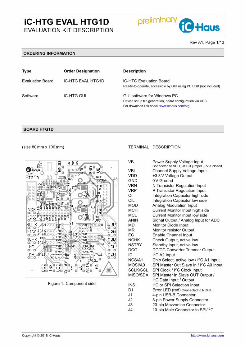
(size 80 mm x 100 mm) TERMINAL DESCRIPTION
Figure 1: Component side
VB Power Supply Voltage InputConnected to VDD_USB if jumper JP2-1 closed.
VBL Channel Supply Voltage InputVDD +3.3 V Voltage OutputGND 0 V GroundVRN N Transistor Regulation InputVRP P Transistor Regulation InputCI Integration Capacitor high sideCIL Integration Capacitor low sideMOD Analog Modulation InputMCH Current Monitor Input high sideMCL Current Monitor Input low sideANIN Signal Output / Analog Input for ADCMD Monitor Diode InputMR Monitor resistor OutputEC Enable Channel InputNCHK Check Output, active lowNSTBY Standby input, active lowDCO DC/DC Converter Trimmer OutputID I2C A2 InputNCS/A1 Chip Select, active low / I2C A1 InputMOSI/A0 SPI Master Out Slave In / I2C A0 InputSCLK/SCL SPI Clock / I2C Clock InputMISO/SDA SPI Master In Slave OUT Output /
I2C Data Input / OutputINS I2C or SPI Selection InputD1 Error LED (red) Connected to NCHK.J1 4-pin USB-B ConnectorJ2 3-pin Power Supply ConnectorJ3 20-pin Mezzanine ConnectorJ4 10-pin Male Connector to SPI/I2C
Copyright © 2018 iC-Haus http://www.ichaus.com
preliminary preliminary iC-HTG EVAL HTG1DEVALUATION KIT DESCRIPTION
Rev A1, Page 2/13
RELATED DOCUMENTS
• IC Documentation→ http://www.ichaus.de/htg
• GUI software for Windows PC: check here for down-load links→ http://www.ichaus.de/htg
PC USB CABLE
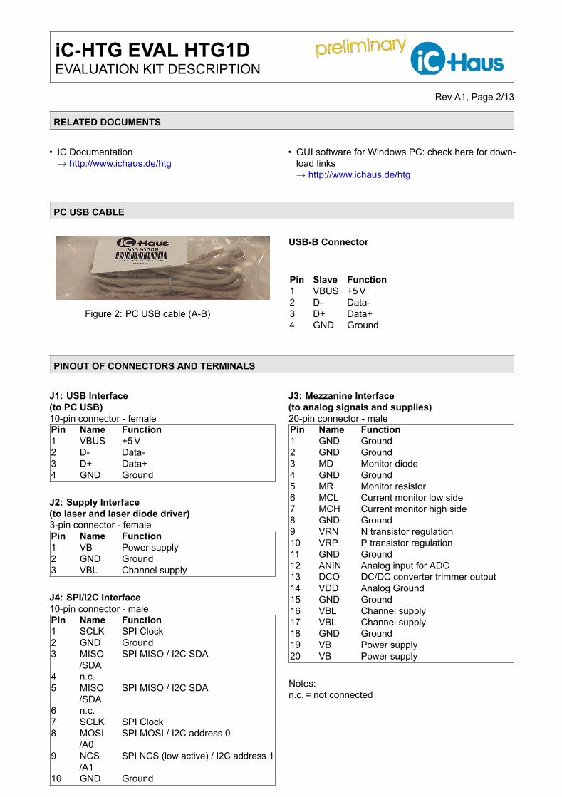
Figure 2: PC USB cable (A-B)
USB-B Connector
Pin Slave Function1 VBUS +5 V2 D- Data-3 D+ Data+4 GND Ground
PINOUT OF CONNECTORS AND TERMINALS
J1: USB Interface(to PC USB)10-pin connector - femalePin Name Function1 VBUS +5 V2 D- Data-3 D+ Data+4 GND Ground
J2: Supply Interface(to laser and laser diode driver)3-pin connector - femalePin Name Function1 VB Power supply2 GND Ground3 VBL Channel supply
J4: SPI/I2C Interface10-pin connector - malePin Name Function1 SCLK SPI Clock2 GND Ground3 MISO
/SDASPI MISO / I2C SDA
4 n.c.5 MISO
/SDASPI MISO / I2C SDA
6 n.c.7 SCLK SPI Clock8 MOSI
/A0SPI MOSI / I2C address 0
9 NCS/A1
SPI NCS (low active) / I2C address 1
10 GND Ground
J3: Mezzanine Interface(to analog signals and supplies)20-pin connector - malePin Name Function1 GND Ground2 GND Ground3 MD Monitor diode4 GND Ground5 MR Monitor resistor6 MCL Current monitor low side7 MCH Current monitor high side8 GND Ground9 VRN N transistor regulation10 VRP P transistor regulation11 GND Ground12 ANIN Analog input for ADC13 DCO DC/DC converter trimmer output14 VDD Analog Ground15 GND Ground16 VBL Channel supply17 VBL Channel supply18 GND Ground19 VB Power supply20 VB Power supply
Notes:n.c. = not connected
preliminary preliminary iC-HTG EVAL HTG1DEVALUATION KIT DESCRIPTION
Rev A1, Page 3/13
DESCRIPTION OF JUMPERS
Jumper JP1 FunctionClosed Shield USB to GND grounded
.Open Shield USB to GND not grounded
(recommended, default).
Jumper JP2-1 FunctionClosed 5V_USB supplies VB by USB connec-
tor J1.Open Keeps separate USB 5 V and VB
(recommended, default).
Jumper JP2-2 FunctionClosed GNDD to GND grounded
(recommended, default).Open GNDD to GND not grounded.
Jumper JP2-3 FunctionClosed VDD supplies VDD_IO of USB device
U4.Open USB device U4 uses default VDD_IO
of 5 V(recommended, default).
Jumper JP2-4 FunctionClosed SCLK_U of USB device U4 con-
nected to SCLK(recommended, default).
Open Keeps SCLK input open.
Jumper JP2-5 FunctionClosed MOSI_U of USB device U4 connected
to MISO_SDA.Open Keeps MISO_SDA input open
(recommended, default).
Jumper JP2-6 FunctionClosed MOSI_U of USB device U4 connected
to MOSI_A0(recommended, default).
Open Keeps MOSI_A0 input open.
Jumper JP2-7 FunctionClosed MISO_U of USB device U4 connected
to MISO_SDA(recommended, default).
Open Keeps MISO_SDA input open.
Jumper JP2-8 FunctionClosed NCS_U of USB device U4 connected
to NCS_A1(recommended, default).
Open Keeps NCS_A1 input open.
Jumper JP2-9 FunctionClosed ANIN_U of USB device U4 connected
to ANIN.Open Keeps ANIN input open
(recommended, default).
Jumper JP2-4 FunctionClosed NCHK_U of USB device U4 con-
nected to NCHK.Open Keeps NCHK input open
(recommended, default).
Jumper JP3 FunctionClosed VB supplies VBL
(recommended, default).Open Keeps individual VB and VBL.
Jumper JP4 FunctionClosed Disables R9 shunt
(recommended, default).Open Enables R9 shunt.
Jumper JP5 FunctionClosed enables LDAP path.Open Keeps LDAP path open
(recommended, default).
Jumper JP6 FunctionClosed Disables R10 shunt.Open Enables R10 shunt
(recommended, default).
Jumper JP7 FunctionClosed Enables LDCN path.Open Keeps LDCN path open
(recommended, default).
Jumper JP8 FunctionClosed Enables VRN path.Open Keeps VRN input open
(recommended, default).
preliminary preliminary iC-HTG EVAL HTG1DEVALUATION KIT DESCRIPTION
Rev A1, Page 4/13
Jumper JP9 Function1-2 Closedleft-middle
Connects low side of R10 to MCL in-put(recommended, default).
2-3 Closedmiddle-right
Connects low side of R9 to MCL input.
Open Keeps MCL input open.
Jumper JP10 Function1-2 Closedleft-middle
Connects high side of R10 to MCHinput(recommended, default).
2-3 Closedmiddle-right
Connects high side of R9 to MCH in-put.
Open Keeps MCH input open.
Jumper JP11 FunctionClosed Connects VDD to EC input
(recommended, default).Open Keeps EC input open.
Jumper JP12 FunctionClosed Connects VDD to ID input.Open Keeps ID input open
(recommended, default).
Jumper JP13 FunctionClosed Connects VB to NCHK input
(recommended, default).Open Keeps NCHK input open.
Jumper JP14 Function1-2 Closedmiddle-right
Connects GND to INS/WKR input(recommended, default).
2-3 Closedleft-middle
Connects VDD to INS/WKR input.
Open Keeps INS/WKR input open.
Jumper JP15 Function1-2 Closedmiddle-right
Connects GND to MR input.
2-3 Closedleft-middle
Connects VDD to MR input.
Open Keeps MR input open(recommended, default).
Jumper JP16 Function1-2 Closedmiddle-right
Connects MDAN to MD input.
2-3 Closedleft-middle
Connects MDCP to MD input.
Open Keeps MD input open(recommended, default).
Jumper JP17 FunctionClosed Enables VRP path.Open Disables VRP path
(recommended, default).
preliminary preliminary iC-HTG EVAL HTG1DEVALUATION KIT DESCRIPTION
Rev A1, Page 5/13
DEFAULT JUMPER SETTING
The default jumper setting is not instantly usable andthe iC-HTG is not accessible without an external supply.Before any use a dedicated jumper setting and a deviceconnection (shunt and emitting diode) is mandatory.
SPI InterfaceThe default jumper setting provides an SPI based com-munication with the USB serial bridge device on board.The SPI interface is the default interface option of theiC-HTG eval board software. The iC-HTG eval boardsoftware supports SPI and I2C for interface selection.With I2C there are 8 addresses selectable from slave 0. . . slave 7 defined by the A0, A1 and A2 address bitsinput pin states.
Jumper JP2-4 FunctionClosed SCLK_U of USB device U4 con-
nected to SCLK(recommended, default).Required to use the on board USBSPI master.
Jumper JP2-5 FunctionOpen Keeps MISO_SDA input open
(recommended, default).Required to use the on board USBSPI master and no connection be-tween MOSI_U of USB device U4 andMISO_SDA.
Jumper JP2-6 FunctionClosed MOSI_U of USB device U4 connected
to MOSI_A0(recommended, default).Required to use the on board USBSPI master and no connection be-tween MOSI_U of USB device U4 andMOSI_A0.
Jumper JP2-7 FunctionClosed MISO_U of USB device U4 connected
to MISO_SDA(recommended, default).Required to use the on board USBSPI master and no connection be-tween MISO_U of USB device U4 andMISO_SDA
Jumper JP2-8 FunctionClosed NCS_U of USB device U4 connected
to NCS_A1(recommended, default).Required to use the on board USBSPI master and no connection be-tween NCS_U of USB device U4 andNCS_A1.
Power Supply and GNDIt is recommended to define the supply structure viaschematic to ensure the right jumper settings beforeany supply of the devices.
Jumper JP2-1 FunctionOpen Keeps separate USB 5 V and VB
(recommended, default).An external VB power supply is re-quired.
Jumper JP2-2 FunctionClosed GNDD to GND grounded
(recommended, default).The GND connection is required.
Jumper JP2-3 FunctionOpen USB device U4 uses default VDD_IO
of 5 V(recommended, default).
Jumper JP3 FunctionClosed VB supplies VBL
(recommended, default).VB and VBL are not connected forindividual voltages.
Load pathIt is recommended to define the load path via schematicto ensure the right jumper settings before any supply orparameter control.
Jumper JP4 FunctionClosed Disables R9 shunt
(recommended, default).R9 shunt is not used.
preliminary preliminary iC-HTG EVAL HTG1DEVALUATION KIT DESCRIPTION
Rev A1, Page 6/13
Jumper JP5 FunctionOpen Keeps LDAP path open
(recommended, default).LDAP (laser diode anode p-type) isnot connected to M1 p-type transistor.
For ACC or APC control JP5 or JP7 one needs to bejumpered to connect to one of the transistors M1 or M2.
Jumper JP6 FunctionOpen Enables R10 shunt
(recommended, default).R10 shunt is usable.
Jumper JP7 FunctionOpen Keeps LDCN path open
(recommended, default).LDCN (laser diode catode n-type) isnot connected to M2 n-type transistor.
For ACC or APC control JP7 or JP5 one needs to bejumpered to connect to one of the transistors M2 or M1.
Jumper JP8 FunctionOpen Keeps VRN input open
(recommended, default).VRN is not connected to M2 n-typetransistors gate.
For ACC or APC control JP8 or JP17 one needs to bejumpered to control one of the transistors M2 or M1.
Jumper JP17 FunctionOpen Disables VRP path
(recommended, default).VRP is not connected to M1 p-typetransistors gate.
For ACC or APC control JP17 or JP8 one needs to bejumpered to control one of the transistors M1 or M2.
Monitoring photodiodes current pathThe optional monitor diodes photo current can be usedfor APC in combination with the internal programmablelogarithmic monitoring resistor.
Jumper JP16 FunctionOpen Keeps MD input open
(recommended, default).MD is not connected to the laserdiode D1 MDCP nor to the laser diodeD2 MDNP.
For APC control JP16 needs to be jumpered to 1-2 or2-3 to provide a current from a photodiode.
Shunt monitoring pathThe monitoring shunt position may vary due to config-ured and jumpered current path.
Jumper JP9 Function1-2 Closedleft-middle
Connects low side of R10 to MCL in-put(recommended, default).To monitors R10 lower voltage.
Jumper JP10 Function1-2 Closedleft-middle
Connects high side of R10 to MCHinput(recommended, default).Monitors R10 higher voltage.
Default Enable Channel stateThe drivers channel is controlled by the external ECsignal and the internal state and parameter.
Jumper JP11 FunctionClosed Connects VDD to EC input
(recommended, default).Provides an Enable Channel state(VDD) at the EC input.
For external channel control remove JP11 and providea high signal for enable channel.
ID ControlWith I2C there are 3 ID bits to select 1 of 8 addressesfor this device. With SPI there is no ID use possible.
Jumper JP12 FunctionOpen Keeps ID input open
(recommended, default).Optional ID definition with I2C inter-face operation only.
Default Standby stateThe default state on an open NSTBY pin is low andkeeps the iC-HTG device in a standby state. To leavethe standby state actively You need to provide a highsignal at the NSTBY pin.
Jumper JP13 FunctionClosed Connects VB to NCHK input
(recommended, default).Device is not in STANDBY and forready for operation.
For external standby control remove JP13 and providea high signal for no standby.
Interface selection SPIThe serial interface can be selected by pin and jumperor signal.
preliminary preliminary iC-HTG EVAL HTG1DEVALUATION KIT DESCRIPTION
Rev A1, Page 7/13
Jumper JP14 Function1-2 Closedmiddle-right
Connects GND to INS/WKR input(recommended, default).SPI interface mode is selected for de-fault interface.
MISC I/O of USB to serial deviceOptional I/O pins of the USB to serial device are pre-pared to be used by PC software.
Jumper JP2-9 FunctionOpen Keeps ANIN input open
(recommended, default).The ANIN_U of USB device U4 is notconnected to ANIN.
The ANIN I/O pin is free to be used.
Jumper JP2-4 FunctionOpen Keeps NCHK input open
(recommended, default).The NCHK_U of USB device U4 notconnected to NCHK.
USB shield to GNDDThe USB-B connectors shield can be connected toGND.
Jumper JP1 FunctionOpen Shield USB to GND not grounded
(recommended, default).This jumper is a solderable bridgingoption.
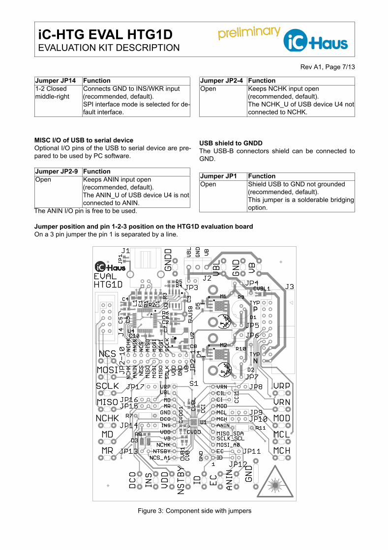
Jumper position and pin 1-2-3 position on the HTG1D evaluation boardOn a 3 pin jumper the pin 1 is separated by a line.
Figure 3: Component side with jumpers
preliminary preliminary iC-HTG EVAL HTG1DEVALUATION KIT DESCRIPTION
Rev A1, Page 8/13
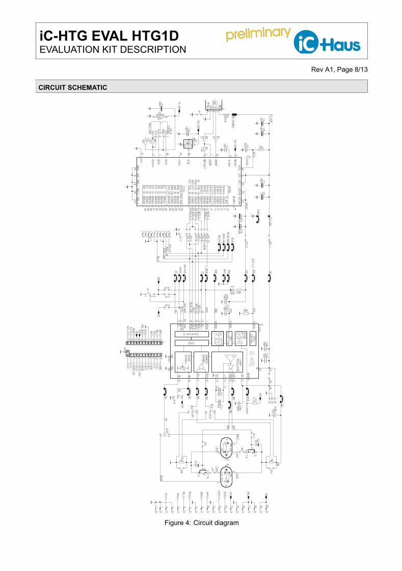
CIRCUIT SCHEMATIC
Figure 4: Circuit diagram
preliminary preliminary iC-HTG EVAL HTG1DEVALUATION KIT DESCRIPTION
Rev A1, Page 9/13
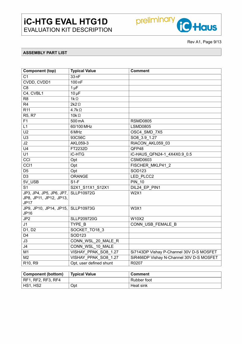
ASSEMBLY PART LIST
Component (top) Typical Value CommentC1 33 nFCVDD, CVDD1 100 nFC8 1µFC4, CVBL1 10µFR8 1kΩR4 2k2Ω
R11 4.7kΩR5, R7 10kΩF1 500 mA RSMD0805L1 60/100 MHz LSMD0805U2 6 MHz OSC4_SMD_7X5U3 93C56C SO8_3.9_1.27J2 AKL059-3 RIACON_AKL059_03U4 FT2232D QFP48U1 iC-HTG iC-HAUS_QFN24-1_4X4X0.9_0.5CCI Opt CSMD0603CCI1 Opt FISCHER_MKLP41_2D5 Opt SOD123D3 ORANGE LED_PLCC25V_USB S1-F PIN_10S1 S2X1_S11X1_S12X1 DIL24_EP_PIN1JP3, JP4, JP5, JP6, JP7,JP8, JP11, JP12, JP13,JP17
SLLP10972G W2X1
JP9, JP10, JP14, JP15,JP16
SLLP10973G W3X1
JP2 SLLP209720G W10X2J1 TYPE_B CONN_USB_FEMALE_BD1, D2 SOCKET_TO18_3D4 SOD123J3 CONN_WSL_20_MALE_RJ4 CONN_WSL_10_MALEM1 VISHAY_PPAK_SO8_1.27 Si7143DP Vishay P-Channel 30V D-S MOSFETM2 VISHAY_PPAK_SO8_1.27 SiR466DP Vishay N-Channel 30V D-S MOSFETR10, R9 Opt, user defined shunt R0207
Component (bottom) Typical Value CommentRF1, RF2, RF3, RF4 Rubber footHS1, HS2 Opt Heat sink
preliminary preliminary iC-HTG EVAL HTG1DEVALUATION KIT DESCRIPTION
Rev A1, Page 10/13
EVALUATION SOFTWARE
iC-HTG software for PCs running on Windows® operating systems as well as the required USB driver are availableas a ZIP file. iC-Haus software built with LabVIEW™ requires the installation of the LabVIEW™ Run-Time Engine(RTE). The RTE must be installed only once, hence there are two download links available.
Software overview online: http://www.ichaus.de/software
Download package without RTE (small size) including RTE (big size)iC-HTG: http://www.ichaus.de/HTG_gui http://www.ichaus.de/HTG_gui_rte
Features• IC configuration made easy by parameter tables and tool tips• Editing of application-specific default setups (*.hex) with CRC calculation• Access to DUT and transfer of setup data to RAM and/or EEPROM• Storage of IC setups as intel® hex file for programming devices
Installation
After unzipping the iC-HTG software package HTG1SO_gui_xx resp. HTG1SO_gui_xxrte, the following files arelocated in the selected working directory (xx is a placeholder for revisions):
→ Subfolder HTG1SO_gui_xx including the executable setup.exe which starts the installation routine.→ Driver package for eval board.
Notice: Administrator rights are required to run installations.
1. To access the iC-HTG evaluation board, interface eval board drivers for USB needs to be installed. The driverinstallation must be completed successfully before connecting the eval board to your PC.→ Execute the USB_xx.exe installation package and follow the on-screen instructions. This can take a fewminutes.
1.1 To complete the driver installation procedure, the eval board must be connected to USB finally, after driverinstallation (only required if the USB interface of the eval board will be used).
2. Install the evaluation software HTG1SO by executing the setup.exe located in the subfolder HTG1SO_gui_xx.→ Follow the on-screen instructions to finish the installation.
3. After installation the executable HTG1SO_gui_xx.exe will be available in the selected working directory.
LabVIEW™ is a trademark of National Instruments.intel® is a trademark of Intel Corporation.Windows® is a trademark of Microsoft Corporation.
preliminary preliminary iC-HTG EVAL HTG1DEVALUATION KIT DESCRIPTION
Rev A1, Page 11/13
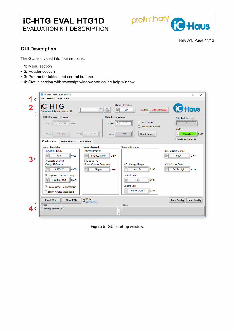
GUI Description
The GUI is divided into four sections:
• 1: Menu section• 2: Header section• 3: Parameter tables and control buttons• 4: Status section with transcript window and online help window.
Figure 5: GUI start-up window.
preliminary preliminary iC-HTG EVAL HTG1DEVALUATION KIT DESCRIPTION
Rev A1, Page 12/13
Menu Button Description
1 Menu Section
<File> Save Config File Saves the configuration to a file, Intel Hex file format (*.hex)Load Config File Loads the configuration to the IC, Intel Hex file format (*.hex)Exit Quits the software
<Interface> No Hardware Disconnects the board and resets the communication betweenPC and eval board.
iC-Interface ↔ SPI Selection for SPI setup of HTG1D, SPI is the default jumperedinterface.
iC-Interface ↔ I2C Selection for I2C setup of HTG1D, Slave range 0 . . . 7.Interface Options→ Connect & Read Checked: connects the eval board and reads the IC registers.
Unchecked: connects the eval board without reading the ICregisters.
<Extras> Parameter Search Enables a search field to locate a parameter’s control field. Ifa name match is found, the corresponding control field will behighlighted and focused.
Generate Report Generates a *report.zip archive reporting the current softwarestatus. This report eases debugging software issues by theiC-Haus’ support team.
About GUI and DLL release information
2 Header Section Project title, chip version, software version and connection state
3 Parameter Section Parameter configuration, read/write access to IC.
<Tabs> Configuration Refer to IC datasheet.Status Monitor Refer to IC datasheet.Hex Editor This tab is a different view of the IC’s register content in HEX
format. Changes made are not automatically updated to the othertabs. Push <Read RAM> to update the parameter tabs.
<Parameter> Read RAM Reads all parameters from the IC and refreshes the display.Write RAM Writes all parameters from GUI to IC RAM.Write Immediately If checked, any change to a parameter is transferred immediately.
If disabled, the GUI can be used stand-alone without hardware.Save Config File Saves the configuration to a file, intel Hex file format (*.hex)Load Config File Loads the configuration to the IC, intel Hex file format (*.hex)
4 Status Section Transcript and feedback messages of user actions.
The GUI software starts with <Interface> Disconnected.When moving the mouse cursor across an input box, a tooltip comes up and displays the real parameter nameaccording to this box. If a functional parameter description is required, please refer to the IC datasheet.

preliminary preliminary iC-HTG EVAL HTG1DEVALUATION KIT DESCRIPTION
Rev A1, Page 13/13
REVISION HISTORY
Rel. Rel. Date∗ Chapter Modification PageA1 2018-02-15 ... Initial release
iC-Haus expressly reserves the right to change its products and/or specifications. An Infoletter gives details as to any amendments and additions made to therelevant current specifications on our internet website www.ichaus.com/infoletter and is automatically generated and shall be sent to registered users by email.Copying – even as an excerpt – is only permitted with iC-Haus’ approval in writing and precise reference to source.
The data specified is intended solely for the purpose of product description and shall represent the usual quality of the product. In case the specifications containobvious mistakes e.g. in writing or calculation, iC-Haus reserves the right to correct the specification and no liability arises insofar that the specification was froma third party view obviously not reliable. There shall be no claims based on defects as to quality in cases of insignificant deviations from the specifications or incase of only minor impairment of usability.No representations or warranties, either expressed or implied, of merchantability, fitness for a particular purpose or of any other nature are made hereunderwith respect to information/specification or the products to which information refers and no guarantee with respect to compliance to the intended use is given. Inparticular, this also applies to the stated possible applications or areas of applications of the product.
iC-Haus products are not designed for and must not be used in connection with any applications where the failure of such products would reasonably beexpected to result in significant personal injury or death (Safety-Critical Applications) without iC-Haus’ specific written consent. Safety-Critical Applicationsinclude, without limitation, life support devices and systems. iC-Haus products are not designed nor intended for use in military or aerospace applications orenvironments or in automotive applications unless specifically designated for such use by iC-Haus.iC-Haus conveys no patent, copyright, mask work right or other trade mark right to this product. iC-Haus assumes no liability for any patent and/or other trademark rights of a third party resulting from processing or handling of the product and/or any other use of the product.
Software and its documentation is provided by iC-Haus GmbH or contributors "AS IS" and is subject to the ZVEI General Conditions for the Supply of Productsand Services with iC-Haus amendments and the ZVEI Software clause with iC-Haus amendments (www.ichaus.com/EULA).
∗ Release Date format: YYYY-MM-DD