Embed Size (px)
Citation preview
Technical Library, t^comm, inc.
MSFC No ni-5-51Q-9
IBM No. 66-366-0001
Technical Manual
Switch Selector. Model II
VJ0N72-75854
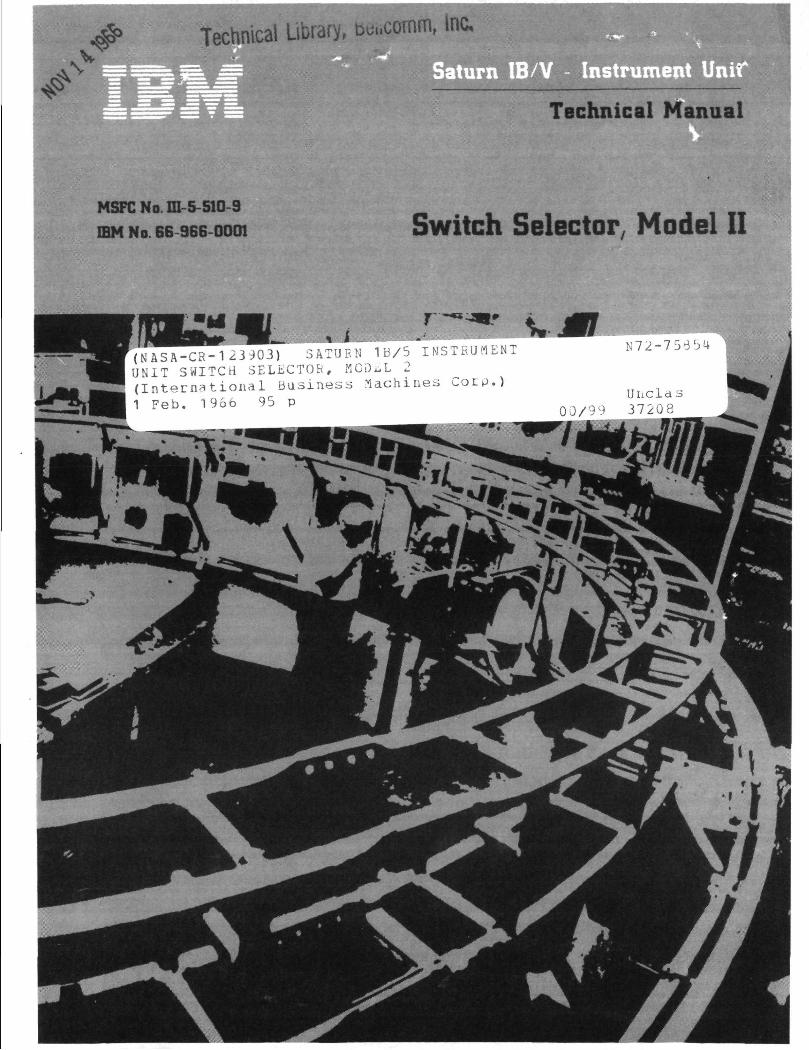
(NASA-CR-123903) SATURN 1B/5UNIT SWITCH SELECTOR, MCDuL 2(International Business Machines :ocp.)1 Feb. '1966 95 p
UucldOJ/99 37206
MSFC No. 111-5-510-9
IBM No. 66-966-0001
TECHNICAL MANUAL
SATURN IB/V INSTRUMENT UNIT
SWITCH SELECTOR, MODEL II
Prepared under Contract
NAS 8-14OOO
by
International Business Machines Corporation
Federal Systems Division
Huntsville, Alabama
1 February 1966
^Tecrtnica! Library, Bellcomm, fnc.
LIST OF EFFECTIVE PAGES
Page Issue
Title OriginalA Originali thru iii Originaliv Blank OriginalI thru 9 Original10 Blank OriginalII thru 13 Original14 Blank Original15 thru 31 Original32 Blank Original33 Original34 Blank Original35 thru 39 Original40 Blank Original41 Original42 Blank Original43 Original44 Blank Original45 Original46 Blank Original47 Original48 Blank Original49 Original50 Blank Original51 Original52 Blank Original53 Original54 Blank Original55 Original56 Blank Original57 Original58 Blank Original59 Original60 Blank Original61 Original62 Blank Original63 Original64 Blank Original65 Original66 Blank Original67 Original68 Blank Original69 Original70 Blank Original71 Original72 Blank Original73 Original74 Blank Original75 Original76 Blank Original77 Original78 Blank Original79 Origina80 Blank Origina81 Origina82 Blank Origina83 thru 85 Origina86 Blank Origina87 Origina
JINSERT LATEST CHANGED PAGES, DESTROY SUPERSEDED PAGES
NOTE: The portion of the text affected by the changes is indicatedby a vertical line in the outer margins of the page.
* The asterisk indicates pages changed, added, or deleted by the current change.

COMMENT SHEET
Your comments will help improve this publication. The followingcomment sheets are provided for your comments on the usefulnessand readability of this publication. Also, suggest additions anddeletions, and indicate any specific errors or omissions. Pleaseforward the completed comment sheet to the following address:
ManagerDepartment 966IBM CorporationHuntsville FacilitySpace Systems CenterHuntsville, Alabama

Manual Title
Manual Number Change Date
Comments
Name _
Address

Manual Title
Manual Number Change Date
Comments
Name
Address
Switch SelectorList of Related Documents
LIST OF RELATED DOCUMENTS
The manuals listed below have been published under NASAcontracts as source and reference information on IU systemsand/or components.
Title
Saturn IB/V Instrument UnitStructure Repair Manual
Auxiliary Power Distributors
Power Distributor
Emergency Detection SystemDistributor
Control Distributor
Measuring Distributors
56 Volt Power Supply
5 Volt Measuring Voltage Supply
Saturn IB/V Instrument UnitInstrumentation SystemDescription
Switch Selector, Model II
NumberIBM
65-966-0011H
65-966-0013H
65-966-0014H
65-966-0015H
65-966-0016H
65-966-0017H
65-966-0018H
65-966-0019H
65-966-0021H
66-966-0001
MSFC
m-5-510-1
HI-5-510-2
m-5-510-3
m-5-510-4
m-5-510-5
HI-5-510-6
m-5-510-7
IH-5-510-8
IH-5-509-1
m-5-510-9
PublishedDate
1 September 1965
1 October 1965
1 October 1965
1 October 1965
1 October 1965
1 October 1965
1 October 1965
1 October 1965
1 November 1965
1 February 1966
ChangedDate
1 January 1966
1 January 1966
LIST OF SPECIFICATIONS AND PROCEDURESFOR SWITCH SELECTOR, MODEL H
Title Number
Schematic
Switch Selector (Top Drawing)
Design Specification
Acceptance Test Plan
Qualification Test Plan
Unit Outline
6101534
6101400 (50M67864)
6009026
373-66644-05
373-66644-06
6101487
Switch SelectorContents
CONTENTS
Section
ILLUSTRATIONS
TABLES
INTRODUCTION AND DESCRIPTION
Page
ii
iii
II
1-1 Introduction 11-2 Description 21-3 Mechanical Design 21-4 Electrical Characteristics . . . . 61-5 Dimensions and Weight 6
PRINCIPLES OF OPERATION 7
Section Page
2-8 Reset (Forced) 202-9 Read Command 212-10 Reset (Automatic) 212-11 Decoding Matrix 232-12 Output Matrix and Telemetry ... 272-13 Test Outputs 272-14 Circuit Description 292-15 Reference Material 38
m PREPARATION FOR USE ANDSHIPMENT 83
2-12-22-32-42-52-62-7
General Operation 7System Description 7Component Description 8Detailed Operation 16Stage Select 18Input Relays 18Verification 20
3-1 Preparation for Use 833-2 Preparation for Shipment 833-3 Packaging 83
rv PREVENTIVE MAINTENANCEAND RE PAIR 87
4-14-2
Preventive Maintenance 87Repair 87
Number Title
ILLUSTRATIONS
Page Number Title Page
1-1 Switch Selector, Model II 2-9(Three-Quarter View) 1
1-2 Switch Selector Circuit Module 2 2-101-3 Switch Selector Panel Assembly . . . . 3 2-111-4 Switch Selector Electrical 2-12
Assembly 41-5 Switch Selector, Model II 2-13
(Internal View) 52-1 Saturn V Switch Selector 2-14
Configurations 9 2-152-2 LVDC - Switch Selector 2-16
Interconnection Diagram 112-3 Switch Selector Register 2-17
Word Format 12 2-182-4 Switch Selector (Model II) 2-19
Simplified Diagram 13 2-202-5 Automatic Reset Circuitry, 2-21
Simplified Diagram 152-6 Typical Switch Selector 2-22
Timing Diagram 172-7 Stage Select Relay Configuration • • • • 18 2-232-8 Input and Verify Relay Circuitry . . . . 19
Read Command RelayConfiguration 21
Automatic Reset Circuitry 22AG Signal Generation Logic 24Portion of Row NOT Signal
Generation Logic 26Portion of Column Signal
Generation Logic 28Zero Indicate Logic 29Register Test Logic 30Switch Selector Electrical
Schematic Diagram (Sheet 1 of 2) ... 31Four Input AND Circuit (A4) 35PNP Inverter Schematic Diagram . . . . 36NPN Inverter Schematic Diagram . . . . 36Latching Relay Schematic Diagram ... 37Conventional Relay Schematic
Diagram 37Switch Selector Logic Diagram
(Sheet 1 of 6) 39Electrical Schematic, Circuit
Module Type 1, Decode 51
ii
Switch SelectorContents
CONTENTS (Cont)
Number Title Page
2-24 Electrical Schematic, CircuitModule Type 2, Output Driver 53
2-25 Electrical Schematic, CircuitModule Type 3, Read 55
2-26 Electrical Schematic, CircuitModule Type 4, Stage Select 57
2-27 Electrical Schematic, CircuitModule Type 5, Auto Reset 59
2-28 Electrical Schematic, CircuitModule Type 6, AND Logic 61
2-29 Electrical Schematic, CircuitModule Type 7, Decode 63
2-30 Electrical Schematic, CircuitModule Type 8, MiscellaneousDriver 65
2-31 Electrical Schematic, CircuitModule Type 9, MiscellaneousDriver ... 67
Number Title
2-32 Electrical Schematic, CircuitMnrhilo Tvne 1 fl Ponri . . . . .
2-33
2-34
2-35
2-36
2-37
2-38
3-1
Electrical Schematic, CircuitModule Type 11 Read
Electrical Schematic, CircuitModule Type 12, Miscellaneous
Electrical Schematic, Circuit
Electrical Schematic, CircuitModule Type 14, Read
Electrical Schematic, Circuit
Electrical Schematic, CircuitModule Type 16, Stage Select
Packaging Instructions for SwitchSelector Model I
Page
... 69
... 71
... 73
. 75
... 77
• 79
... 81
. 85
Number
TABLES
Title Page
1-1 Types and Use of Switch SelectorCircuit Modules
1-2 Electrical Characteristics . . .2-1 Switch Selector Relay Functions .
2
637
iii/iv
Switch SelectorSection I
SECTION I
INTRODUCTION AND DESCRIPTION
1-1 INTRODUCTION
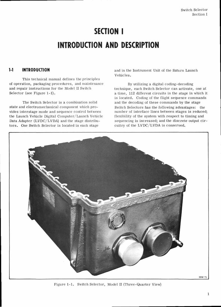
This technical manual defines the principlesof operation, packaging procedures, and maintenanceand repair instructions for the Model II SwitchSelector (see Figure 1-1).
The Switch Selector is a combination solidstate and electromechanical component which pro-vides interstage mode and sequence control betweenthe Launch Vehicle Digital Computer/Launch VehicleData Adapter (LVDC/LVDA) and the stage distribu-tors. One Switch Selector is located in each stage
and in the Instrument Unit of the Saturn LaunchVehicles.
By utilizing a digital coding-decodingtechnique, each Switch Selector can activate, one ata time, 112 different circuits in the stage in which itis located. Coding of the flight sequence commandsand the decoding of these commands by the stageSwitch Selectors has the following advantages: thenumber of interface lines between stages is reduced;flexibility of the system with respect to timing andsequencing is increased; and the discrete output cir-cuitry of the LVDC/LVDA is conserved.
Figure 1-1. Switch Selector, Model II (Three-Quarter View)
Switch SelectorSection I
1-2 DESCRIPTION
1-3 ME C HANICA L DE SIGN
The mechanical design of the Switch Selectoris comprised of a housing, cover, cover gasket, andan electrical assembly. The electrical assemblyconsists of two panel assemblies, a harness assembly,two RFI filters, and 34 circuit modules. There are4, 684 discrete electrical components packaged inthe circuit modules.
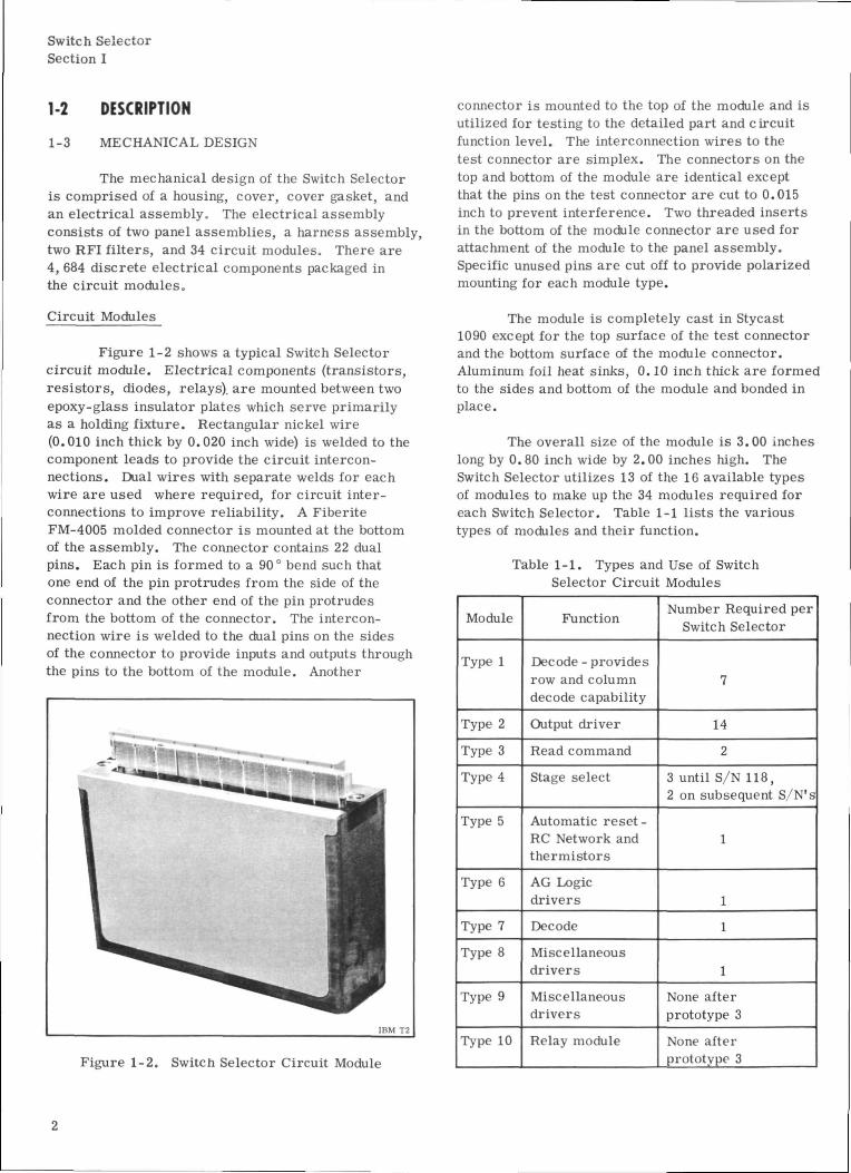
Circuit Modules
Figure 1-2 shows a typical Switch Selectorcircuit module. Electrical components (transistors,resistors, diodes, relays), are mounted between twoepoxy-glass insulator plates which serve primarilyas a holding fixture. Rectangular nickel wire(0.010 inch thick by 0.020 inch wide) is welded to thecomponent leads to provide the circuit intercon-nections. Dual wires with separate welds for eachwire are used where required, for circuit inter-connections to improve reliability. A FiberiteFM-4005 molded connector is mounted at the bottomof the assembly. The connector contains 22 dualpins. Each pin is formed to a 90° bend such thatone end of the pin protrudes from the side of theconnector and the other end of the pin protrudesfrom the bottom of the connector. The intercon-nection wire is welded to the dual pins on the sidesof the connector to provide inputs and outputs throughthe pins to the bottom of the module. Another
connector is mounted to the top of the module and isutilized for testing to the detailed part and circuitfunction level. The interconnection wires to thetest connector are simplex. The connectors on thetop and bottom of the module are identical exceptthat the pins on the test connector are cut to 0.015inch to prevent interference. Two threaded insertsin the bottom of the module connector are used forattachment of the module to the panel assembly.Specific unused pins are cut off to provide polarizedmounting for each module type.
The module is completely cast in Stycast1090 except for the top surface of the test connectorand the bottom surface of the module connector.Aluminum foil heat sinks, 0.10 inch thick are formedto the sides and bottom of the module and bonded inplace.
The overall size of the module is 3.00 incheslong by 0.80 inch wide by 2.00 inches high. TheSwitch Selector utilizes 13 of the 16 available typesof modules to make up the 34 modules required foreach Switch Selector. Table 1-1 lists the varioustypes of modules and their function.
Table 1-1. Types and Use of SwitchSelector Circuit Modules
Figure 1-2. Switch Selector Circuit Module
Module
Type 1
Type 2
Type 3
Type 4
Type 5
Type 6
Type 7
Type 8
Type 9
Type 10
Function
Decode - providesrow and columndecode capability
Output driver
Read command
Stage select
Automatic reset -RC Network andthermistors
AG Logicdrivers
Decode
Miscellaneousdrivers
Miscellaneousdrivers
Relay module
Number Required perSwitch Selector
7
14
2
3 until S/N 118,2 on subsequent S/N's
1
1
1
1
None afterprototype 3
None afterprototype 3
Switch SelectorSection I
Table 1-1. Types and Use of SwitchSelector Circuit Modules (Cont)
Module
Type 11
Type 12
Type 13
Type 14
Type 15
Type 16
Function
Relay module
Miscellaneousdriver
Relay module
Relay module
Decode - switchpower, zeroindicate, andcolumn 02
Relay module
Number Required perSwitch Selector
1
None after S/N 104
1
1
1
1 after S/N 117
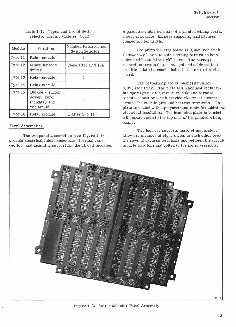
Panel Assemblies
The two panel assemblies (see Figure 1-3)provide electrical interconnections, thermal con-duction, and mounting support for the circuit modules.
A panel assembly consists of a printed wiring board,a heat-sink plate, harness supports, and harnessconnection terminals.
The printed wiring board is 0.062 inch thickglass-epoxy laminate with a wiring pattern on bothsides and "plated through" holes. The harnessconnection terminals are swaged and soldered intospecific "plated through" holes in the printed wiringboard.
The heat-sink plate is magnesium alloy0.091 inch thick. The plate has machined rectangu-lar openings at each circuit module and harnessterminal location which provide electrical clearancearound the module pins and harness terminals. Theplate is coated with a polyurethane resin for additionalelectrical insulation. The heat-sink plate is bondedwith epoxy resin to the top side of the printed wiringboard.
Two harness supports made of magnesiumalloy are mounted at right angles to each other overthe rows of harness terminals and between the circuitmodule locations and bolted to the panel assembly.
u i i.; i s ri - i l . i l . i-* ... i •* •/• *• ' • 4J
Figure 1-3. Switch Selector Panel Assembly
Switch SelectorSection I
Harness Assembly
The harness is a conventional branched typeutilizing 26 AWG tinned copper, polyolefin insulated,wire. The harness is layed out, formed, laced, andunit connectors attached prior to installation on theelectrical assembly.
Harness wires are dual redundant for in-creased reliability. At the unit connector, eachpair of redundant wires is terminated in one contactwith a crimp and a solder connection. The back ofthe unit connectors are potted with a polyurethanecompound to provide a seal and strain relief for thewires.
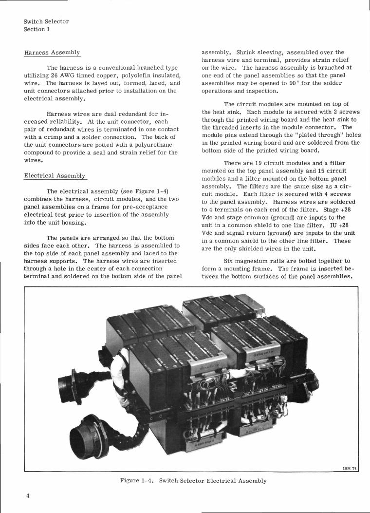
Electrical Assembly
The electrical assembly (see Figure 1-4)combines the harness, circuit modules, and the twopanel assemblies on a frame for pre-acceptanceelectrical test prior to insertion of the assemblyinto the unit housing.
The panels are arranged so that the bottomsides face each other. The harness is assembled tothe top side of each panel assembly and laced to theharness supports. The harness wires are insertedthrough a hole in the center of each connectionterminal and soldered on the bottom side of the panel
assembly. Shrink sleeving, assembled over theharness wire and terminal, provides strain reliefon the wire. The harness assembly is branched atone end of the panel assemblies so that the panelassemblies may be opened to 90 ° for the solderoperations and inspection.
The circuit modules are mounted on top ofthe heat sink. Each module is secured with 2 screwsthrough the printed wiring board and the heat sink tothe threaded inserts in the module connector. Themodule pins extend through the "plated through" holesin the printed wiring board and are soldered from thebottom side of the printed wiring board.
There are 19 circuit modules and a filtermounted on the top panel assembly and 15 circuitmodules and a filter mounted on the bottom panelassembly. The filters are the same size as a cir-cuit module. Each filter is secured with 4 screwsto the panel assembly. Harness wires are solderedto 4 terminals on each end of the filter. Stage +28Vdc and stage common (ground) are inputs to theunit in a common shield to one line filter. IU +28Vdc and signal return (ground) are inputs to the unitin a common shield to the other line filter. Theseare the only shielded wires in the unit.
Six magnesium rails are bolted together toform a mounting frame. The frame is inserted be-tween the bottom surfaces of the panel assemblies.
Figure 1-4. Switch Selector Electrical Assembly
Switch SelectorSection I
The panel assemblies are bolted to the frame. Atemporary test harness is attached to the electricalassembly for pre-acceptance testing. The testharness wires are attached to 61 terminals on thepanel assemblies in the same manner as the systemharness. After completion of pre-acceptance test,the test harness wires are cut off just above thetest terminals and the harness is removed. Shrinksleeving is applied over the test terminals to sealthem.
Housing, Cover, and Gasket
The component housing is a magnesium alloycasting. There are four unit mounting bosses with0.281-inch diameter mounting holes at each cornerof the casting. The bottom of the bosses is on thesame plane as the bottom surface of the casting.The bosses are 0.250 inch thick. There are mount-ing holes for a 32-contact connector, a 62-contactconnector, a pressure relief valve, and a purgingvalve in one end of the casting. In the other end ofthe casting there are mounting holes for a 32-contactconnector, a 61-contact connector, and a purgingvalve. The top edge of the four side walls of thecasting have 32 tapped holes for cover mounting*Inside the casting there are ten bosses which extendfrom the bottom surface and side walls. Thesebosses have one tapped hole in each for mounting
the electrical assembly. On the bottom inside sur-face of the casting, four silicone sponge pads arebonded with adhesive. These pads are compressedby the circuit modules when the electrical assemblyis inserted and thereby provide additional supportand dampening under mechanical environment. Thecasting is treated with iridite and coated withaluminum paint.
The unit cover is a machined magnesuimalloy plate with 32 clearance holes for mounting.Four silicone pads are bonded to the bottom surfaceof the cover. These pads are compressed when thecover is assembled to the housing by the circuitmodules of the electrical assembly and serve thesame purpose as the pads inside the housing. Thecover is treated with iridite and painted withaluminum paint.
The cover gasket material is silicone filledstainless steel which provides both a pressure sealand RFI shielding. The gasket is 0.062 inch thickby 0.312 inch wide and forms a rectangle to fit thetop edge of the housing. There are 32 clearanceholes for the cover mounting screws.
Component Assembly
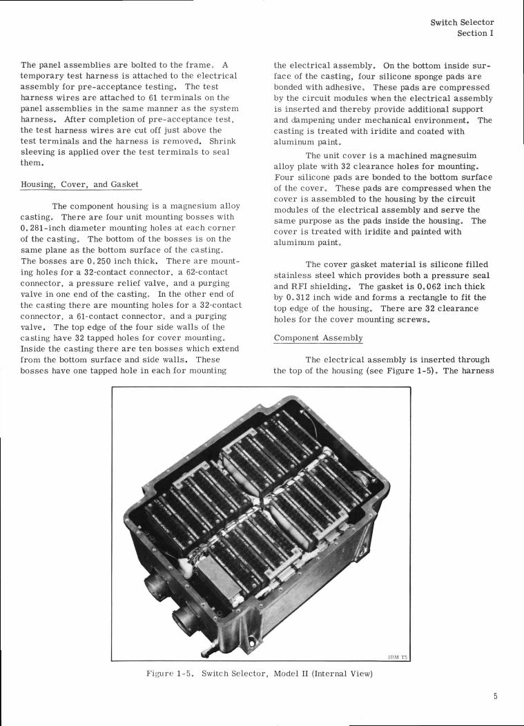
The electrical assembly is inserted throughthe top of the housing (see Figure 1-5). The harness
Figure 1-5. Switch Selector, Model II (Internal View)
Switch SelectorSection I
connectors are drawn through their mounting holesand secured with hexagonal nuts and safety wire.The electrical assembly is bolted in 10 placesto the bosses in the bottom of the housing. Theshield ground wires are secured to the inside sur-face of the housing wall with screws and lockwashers. The pressure relief valve, which is pre-set for a "cracking" pressure of 10 psi, and the twopurging valves are assembled in their mountingholes. The cover gasket and cover are mounted ontop of the housing and secured with 32 screws.
1-4 ELECTRICAL CHARACTERISTICS
The electrical characteristics of the SwitchSelector Model II are specified in Table 1-2.
1-5 DIMENSIONS AND WEIGHTThe Switch Selector has the following physical
characteristics:Height: 5.29 inches maximumWidth: 8.56 inches maximumLength: 12.50 inches maximumWeight: 19.8 pounds (approx)
Table 1-2. Electrical Characteristics
Input Voltages
Verification 28+4 VdcStage supply voltage 2 8 + 2 Vdc
Input Power
Peak 17.6 WattsStandby 1.9 Watts
Input Signals
Stage select "^ Up level: 17.5 VdcRead command (min) to 32.0 Vdc (max)Reset >Down level: open circuit8-bit coded input clamped to gnd for
J negative suppression.
Output Signals
Register verification 28 VdcChannel outputs . 28 VdcZero indicate 28 VdcRegister test 28 VdcTelemetry
No channel active 0.2 VdcOne channel active 2.0 VdcMore than one channel active . 3.0 Vdc
Operating Temperature -25 °C (-13 °F) to+100 °C (+212 °F) in apartial vacuum of notgreater than 10-4 mm
of mercury.
Electrical Isolation „ 100 Megohms between allpoints not connected by aconductor.
Heat Dissipation 3.0 Watts
Switch SelectorSection n
SECTION II
PRINCIPLES OF OPERATION
2-1 GENERAL OPERATION
2-2 SYSTEM DESCRIPTION
Each stage, and the Instrument Unit, of theSaturn Launch Vehicle are equipped with a SwitchSelector. The Switch Selector consists of electronicand electromechanical components which decodedigital flight sequence commands from the LVDA/LVDC and activate the proper stage circuits to ex-ecute the commands.
Each Switch Selector can activate, one at atime, 112 different circuits in its stage. The selec-tion of a particular stage Switch Selector is accom-plished through the command code. Coding of flightsequence commands and decoding of the stage SwitchSelectors reduces the number of interface lines be-tween stages and increases the flexibility of thesystem with respect to timing and sequence. In theSaturn V Launch Vehicle, which contains 4 SwitchSelectors, 448 different functions can be controlledusing only 28 lines from the LVDA. (Two IU + 28-volt and two signal return lines from the ControlDistributor are also used.) Flight sequence com-mands may be issued at time intervals of 100 milli-seconds.
Figure 2-1 illustrates the Saturn V SwitchSelector configuration. As shown, all SwitchSelector control lines are connected through theControl Distributor in the IU to the LVDA and theelectrical support equipment.
To maintain power isolation between vehiclestages, the Switch Selector is divided into twosections: The input section (relay circuits) of eachSwitch Selector receives its power from the IU; theoutput section (decoding circuitry and drivers) ofeach Switch Selector receives its power from thestage in which the Switch Selector is located. Theinput and output are coupled together through a diodematrix. This matrix decodes the 8-bit input codeand activates a PNP output driver, thus producing aSwitch Selector output.
Each Switch Selector is connected to the LVDAthrough 2^8 lines:
tage select lines - 8Read command lines - 2Reset (forced) lines - 2Bit register output lines - 8Verification lines - 8
In addition, there are 2 lines for IU +28 Vdc and 2lines for signal return between the Control Distributorand the Switch Selectors.
The wire pairs for stage select, read com-mand, forced reset, IU + 28 Vdc, and signal returnare redundant. Only one of each pair is requiredfor normal operation.
All connections between the LVDA and theSwitch Selectors, with the exception of the stageselect inputs, are connected in parallel as shown inFigure 2-2.
The output signals of the LVDA switch selec-tor register, with the exception of the 8-bit com-mand, are sampled at the Control Distributor in theIU and sent to IU PCM telemetry. Each SwitchSelector also provides 3 outputs to the telemetrysystem within its stage.
The Switch Selector is designed to executeflight sequence commands given by the 8-bit code orby its complement. This feature increases reli-ability and permits operation of the system despitecertain failures in the LVDA switch selector regis-ter, line drivers, interface cabling, or SwitchSelector relays.
The flight sequence commands are stored inthe LVDC memory and are issued according to theflight program. When a Programmed Input/Output(PIO) instruction is given, the LVDC loads the 15-bitswitch selector register with the computer data.The LVDA switch selector register word format isshown in Figure 2-3.
Switch SelectorSection II
Switch selector register bits 1 through 8represent the flight sequence command. Bits 9through 13 select the Switch Selector to be activated.Bit 14 resets all the relays in the Switch Selectorsin the event data transfer is incorrect as indicatedby faulty verification information received by theLVDA. Bit 15 activates the addressed Switch Selec-tor for execution of the command. The LVDC loadsthe switch selector register in two passes; bits 1through 13 are loaded during the first pass and,depending on the feedback code, either bit 14 or bit15 is loaded during the second pass.
After the Switch Selector input relays havebeen "picked" by the 8-bit command, the comple-ment of the received code is sent back to the LVDA/LVDC over eight parallel lines. The feedback(verification information) is returned to the digitalinput multiplexer of the LVDA and is subsequentlycompared with the original code in the LVDC. If thefeedback agrees with the original code, a read com-mand is given. If the feedback does not agree withthe original code, a reset command is given (forcedreset), and the LVDC/LVDA reissues the 8-bit com-mand in complement form.
A typical operation cycle, to initiate a givenfunction in a particular stage, is accomplished asfollows:
• The 8 verify lines are sampled to ensurethat all stage select relays have beenreset, thereby ensuring an unwantedstage is not selected. Zero voltage onall lines indicates that this conditionexists. The presence of IU + 28 Vdc onthe verify lines indicates that the verifylines are enabled because a stage SwitchSelector is not reset. Having detectedthis situation, the LVDC commands a"force reset" and then rechecks theverify lines.
• The LVDC inserts the 8-bit flight com-mand into the LVDA switch selectorregister. At the same time, a stageselect command is sent to the appropri-ate Switch Selector. Application of thestage select command completes thesignal return path for the input relaysand allows the 8-bit command to bestored in the Switch Selector input relays.
• The verification lines are sampled to de-termine if the command transfer wascorrect.
• If the verification is correct, the LVDCsends a read command to the SwitchSelector; activating it, and causing theproper output to occur.
• If the verification is not correct, theLVDC initiates a reset command toprepare the Switch Selector to receivethe complement of the original command.
• After the forced reset is completed, theLVDC loads the stage select command,and the complement of the previouslysent command, into the LVDA switchselector register.
• Neglecting the verification informationthat occurs after the complement com-mand is inserted, the LVDC initiates aread command which produces an outputfrom the selected switch selectorchannel. The read command also ener-gizes the automatic reset circuitry whichreturns the Switch Selector to the resetcondition to prepare it for a new cycle.
2-3 COMPONENT DESCRIPTION
A description of Switch Selector operation isgiven in the following paragraphs (refer to thesimplified schematic diagram shown in Figure 2-4).The circuit functions of the Switch Selector are asfollows:
Stage select
Input relays
Verification
Reset (forced)
Read command
Reset (automatic)
Decoding matrix
Output matrix and telemetry
Test outputs
Switch SelectorSection II
0)"^
"^i_ " " ~N
° 1 -O0 <3 +uj.n-J
oj
"2 1,C „ <u
3 'Eg0) ^ <U
*- £ « cr- • m • —
o> S 1 » -3 3 *- -aP D) 5 ° <
*" .2 c 53
4_ C lj\ "™
U ~ " J
^ ^ 8 ,.c „ u g _ .'
J ° g ° .E ~
J! ° .1 0 ™ 1•= < 0 -0 .'
o>!:5 I <£ li - -§ | "> o O ° O£ -= " * o
— O <1> C * .
£ . = Q- =63 l_ w» |•J; £ u o oo u
D aj t5 J " 'D 'C — 0 o 0 -i
o> «_g ^"a3C^ 5f c-o
"o
1-zUJ
_i a.
35
g2;3ouj oL
Q-
LO
r r r r ^ ^ ^O ,13 y "u <U tm^ O) -C
1 1 i 1 1 1 1 1
- c o
1/5
^
? C x
3 •*- t> x
^ 0 1 0 ) ^13 ^ — P -C *.
:_j j | -i § 5: .E _ u c £ g, .E S: - + --8 ^ f- ErT.c g-B 1 ,2"" |DO » a> D c |
2 0 C. 8 _ ^ <U
" £C "" D> + -' 4-^*"
j > ! ' " ^ oJ 'So-S' . i~ 4) O ° 0) c "D
5 a> «> ^ — ' \ v S5 S J CN
ll n u n ll u II u n3 O "O (U u- O5-C •— j-^ £
XU
m ^F rfli
l-
o
x
^
^
^
^
i.
V
01.^^3
3
/-C
^
1
j
•
f
-Cu
Jk
UQ
_l
C
1c
u
L(1
,>
rL
>
rD
*c
s.
/
c
'c0
_
u
V—
5)a>•£
V
(
i
3
O
£)
5
^
c
3 <
^J
N
n -i
i
2t.
j
>L-
\
3
3
;
i
u.
1 R
ece
ive
r
'
• D
a_ i
i
5 -C
j'
C
uT3
corCM V
• i
: i
\
- ":
>-
j
i
t>«
^1-«
i
'
^
/(
i
u<1>L
5
- E
^
N
" "^31 ~>
D -*'
0 — '
b -^
_^ J)
^S
<
•y^
1
O
£S-D
5
JO
^ m uj -uj O O (X/r\ ^ \J i_J
< S - ^- ^ n ^
> j
nvj (ifiV? f{(Vii ({(*v*u t 3 u " o 6 - * - u - » -
<^J) t^Ji t ^ o j t n a >
V !' v., \< V v " V >
| f^ | j f. 1 | £„ | jIT ( U ' ^ t c x i ' ^ v ^ C N ' t <U "2j CM "^
" 5 ' " O J ' D - o o > * 5 ' " - Q Q J ' ^
C N P 0 , ^ ^ P ° ^ < N P 0 ^ 0 ^
1
^S^x' "xSjX' "^^^x' "S^^^x"
f|j l|}' ||j |!j
Figure 2-1. Saturn V Switch Selector Configuration
9/10
The Switch Selector operates on positivelogic (i. e., + 28 Vdc for a binary "1" and 0 Vdc fora binary "0").
Stage Select
The purpose of the stage select command isto enable the desired Switch Selector to receive thecoded flight sequence command from the LVDA. The
Switch SelectorSection H
stage select command (1 bit) is transmitted individ-ually on a separate line to each Switch Selector. Be-cause of the danger of overloading the LVDA, nomore than 2 Switch Selectors can be addressedsimultaneously.
The stage select command sets three mag-netic latch relays in the addressed Switch Selector.The setting of these relays completes a ground path
LVDC
1
LVDA
1 Stage Select
| 12 | 9 | 10 | 11 | 13
(Spare)
ControlDistributor
Notes:
1. 221LVC
2. 261LVC
3. 28LVC
15-Bit Serial " 8-Bit Serial
1
|
Flight "*Command | Reset | Read |
1 t h rough 8 | 14 | 15 |
*
<—*•
:
1
8 LinesParallel
•
•
>
•
y \
(
{
t
4
f 1
I
i t
i 1
1
' 1
i I
1
4
r 1
I i
i i
i 1
'
Digital InputMultiplexer
| 1 th rough 8
, Signal ^Return
\
IU+28 V
O 1
1
i |
i |
1
4
' 1
i i
I
I
\, 6D COM
Hr
1
<
1
•
1
i
. i
'
•
(
k J
•f
L
'
1
J
8 LinesParallel
1
1
1
'
-
"""" IDSwitchSelector
S-IVBSwitchSelector
b-llSwitch
_ Selector
SwitchSelector
ines between each Switch Selector and 4. 30 lines (maximum number)available to SwitchA. Selectors from LVDA (5 Switch Selectors).
ines between all Switch Selectors and 5. 4 lines (IU +28 Vdc and signal return) to allA (Saturn IB) (3 Switch Selectors). Switch Selectors from Control Distributor
(Saturn IB and V).ines between all Switch Selectors andA (Saturn V) (4 Switch Selectors).
IBMT7
Figure 2-2. LVDC - Switch Selector Interconnection Diagram
11
Switch SelectorSection n
1 2 3 4 5 6 7 8
CommandBits
9 10 11 12J13
Stage select(One bit per stage
others are spare)
14
c5•*-
15
5-o
IBM T8
Figure 2-3. Switch Selector Register Word Format
for the read command relay, the set side of the in-put relays, and the verify power relay (see Figure2-4). This action conditions the read and inputrelays to receive commands from the LVDA andenergizes the verify power relay. When the verifypower relay contacts close, IU + 28 Vdc power isapplied through a set of stage select contacts to theverify relay contacts; and stage + 28 Vdc is appliedto the verify relays. The Switch Selector can nowaccept the 8-bit command from the LVDA, store itin the input relays, and make verification informa-tion available to the LVDA.
Input Relays
The input register of the Switch Selector ismade up of eight magnetic latch relays, controlledby the 8-bit coded command from the LVDA. Thecoded command (consisting of 8 bits in parallel) isavailable to the Switch Selector during the sameperiod of time the stage select signal is present.As soon as the stage select relays are set, a signalreturn path is provided for the coded commandthrough the input relay coils (see Figure 2-4). Thisallows the coded command to be stored in the inputregister.
Once the coded command is stored in theinput register, binary information is available tothe verification register, column decoder, row de-coder, and the AND gate generator.
Verification
A feedback circuit is used to provide verifi-cation information back to the LVDC. This circuitconsists of 8 relays, and is controlled by the inputrelay contacts. When a "1" is applied to the inputrelay set coil, stage ground is switched to the veri-fy relay set coil causing the normally closed verify
relay contact to open; indicating a "0" to the LVDC.When a "0" is applied to the input relay set coil, theinput relay contacts remain in the reset condition.Stage ground remains applied to one side of theverify relay reset coil, causing the verify relay con-tact to remain in its normally closed position.Therefore, the verification output of a Switch Selec-tor is the complement of the input command.
Read Command
Immediately after verification of the originalcommand, the read command is initiated. If verifi-cation of the original command proved to be false,the read command will not be initiated by the LVDCuntil the forced reset, stage select, and comple-mented command have been transmitted to the SwitchSelector.
Three conventional (non-latching) relays arepicked when the read command is received from theLVDA. One side of the coils of these relays is con-nected to the read command signal, the other side isconnected to the IU signal return through the stageselect relay contacts. Thus, a stage select signalmust have been received before a read commandrelay can be energized. When the read relay con-tacts close, stage ground is applied to the switchpower inverters (SPWRA and SPWRC) in the decodermatrix. These inverters generate voltages (SPWRAand SPWRC) which activate the AND gate generatorsand the column decoder circuitry allowing the codedcommand to be decoded and an output to occur.
Reset (Forced)
A forced reset is initiated by the LVDC whenthe LVDC determines that the verification informa-tion is not the complement of the given command.The reset signal is applied to the forced reset relaycoil causing the forced reset contacts to close.This action applies stage + 28 Vdc to the stageselect and input relay reset coils forcing the SwitchSelector into the reset condition shown in Figure2-4. After the forced reset has been completed,the stage select command and the complement of theoriginal flight sequence command are transmitted tothe Switch Selector. The complement command isnot verified by the LVDC before the read commandis issued.
Reset (Automatic)
An automatic reset pulse is generated whenstage power is initially applied to the Switch Selec-tor and when the read command is issued. The
12
Switch SelectorSection II
RegisterVerificationto LVDA
IU +28 Vdc
ID +28 Vdc Signal ^Return
Stage+28 Vdc"
CommandSignalsFrom LVDASwitchSelectorRegister
ForcedReset
Read-
From LVDASwitchSelectorRegister {Bits 1 thru 8
Set
•*^, \ T' 'V Set
Input Relays (8)
StagSele
•~ Rela(Res
ect
Xs
et)
r ReadComm
["]nand
pH1
^c
--, i
Pwr -Inv
AUTO RESETJ
V.
I
- Force~ Reset
(
A/- 1v^VerifyRelay
(8)
A .VReset
_ Verify~ Power
Bit NOT
_[_Set -
Input< i Relay
Contacts
Reset
Bit *
Stage +28 VdcReturn
Stage+28 Vdc Return
Stage+28 Vdc
Bl
BIN
B7N
B8
B8N
B4
B4N
B5
B5N
B6
B6N
ReadII KNP
I II InvRelays I '
0000
' Stage +28 VdcReturn
SPWRC
AND GATE GENERATOR
Bit AG
HI"-~ Relays
Stage +28 VdcReturn
mi
COLUMN DECODER
Bits —
iAG
Bits —
AG
AG1
AGIN
of 7 Possible Inputs
AG2
AG3
AG4AG5
ROW DECODER
Bits -
AG
Bits -
IAG
OUTPUT MATRIX o
(7X16) °
&
Column
0000
1111
Output ChannelDriver
\
^ZeroIndicate
„ Register'Test
, Sw SelOutput
>To Telemetry
112Outputs
.To Functional
Control Circuits
I of 16 Possible Inputs
Notes: 1. Double-weight lines indicate IU Power;single-weight lines indicate individual stage power.
2. All relays and contacts shown in the reset condition.
*Single Channel ActiveNo Channel ActiveTwo or More Active
= 2.0V ±25%= 0.2V or less= 3.0 V or more
IBM T9
Figure 2-4. Switch Selector (Model H) Simplified Diagram
13/14
Switch SelectorSection n
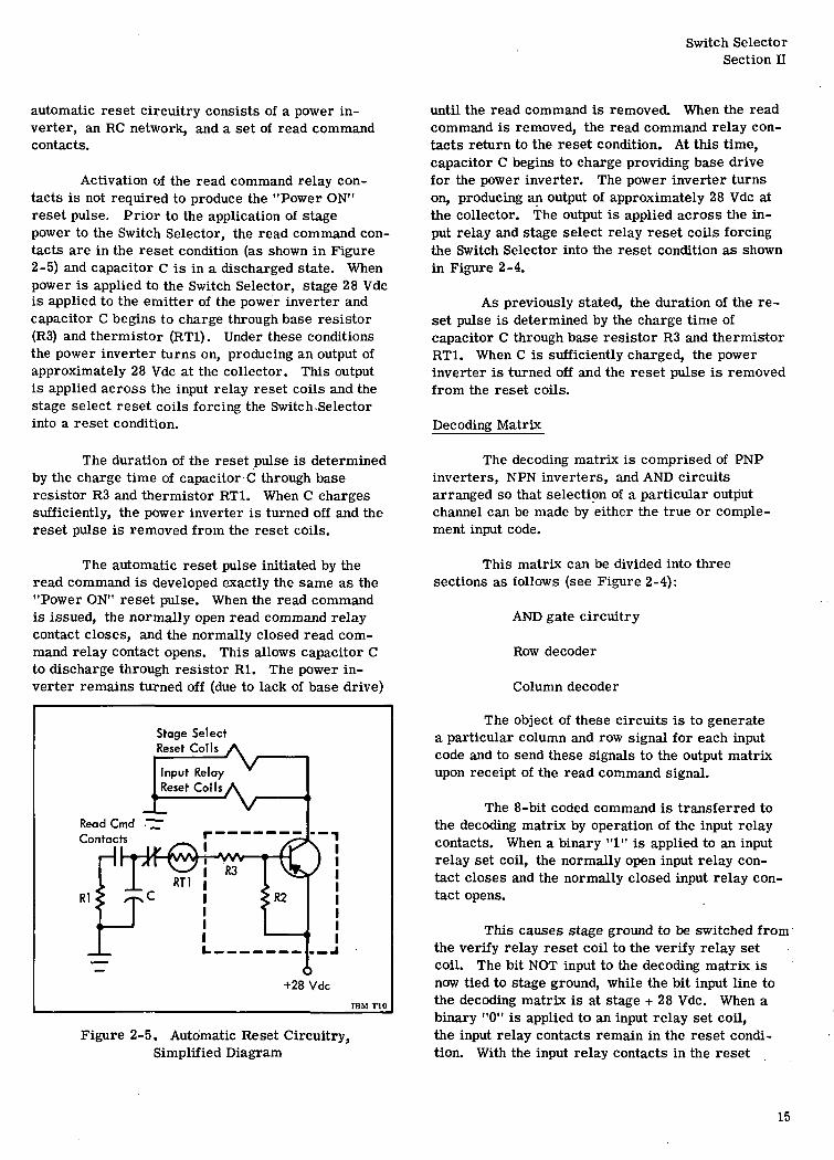
automatic reset circuitry consists of a power in-verter, an RC network, and a set of read commandcontacts.
Activation of the read command relay con-tacts is not required to produce the "Power ON"reset pulse. Prior to the application of stagepower to the Switch Selector, the read command con-tacts are in the reset condition (as shown in Figure2-5) and capacitor C is in a discharged state. Whenpower is applied to the Switch Selector, stage 28 Vdcis applied to the emitter of the power inverter andcapacitor C begins to charge through base resistor(R3) and thermistor (RT1). Under these conditionsthe power inverter turns on, producing an output ofapproximately 28 Vdc at the collector. This outputis applied across the input relay reset coils and thestage select reset coils forcing the Switch-Selectorinto a reset condition.
until the read command is removed. When the readcommand is removed, the read command relay con-tacts return to the reset condition. At this time,capacitor C begins to charge providing base drivefor the power inverter. The power inverter turnson, producing an output of approximately 28 Vdc atthe collector. The output is applied across the in-put relay and stage select relay reset coils forcingthe Switch Selector into the reset condition as shownin Figure 2-4.
As previously stated, the duration of the re-set pulse is determined by the charge time ofcapacitor C through base resistor R3 and thermistorRT1. When C is sufficiently charged, the powerinverter is turned off and the reset pulse is removedfrom the reset coils.
Decoding Matrix
The duration of the reset pulse is determinedby the charge time of capacitor C through baseresistor R3 and thermistor RT1. When C chargessufficiently, the power inverter is turned off and thereset pulse is removed from the reset coils.
The automatic reset pulse initiated by theread command is developed exactly the same as the"Power ON" reset pulse. When the read commandis issued, the normally open read command relaycontact closes, and the normally closed read com-mand relay contact opens. This allows capacitor Cto discharge through resistor Rl. The power in-verter remains turned off (due to lack of base drive)
Stage SelectReset Colls
Read Cmd ~Contacts
IBM T10
Figure 2-5, Automatic Reset Circuitry,Simplified Diagram
The decoding matrix is comprised of PNPinverters, NPN inverters, and AND circuitsarranged so that selection of a particular outputchannel can be made by either the true or comple-ment input code.
This matrix can be divided into threesections as follows (see Figure 2-4):
AND gate circuitry
Row decoder
Column decoder
The object of these circuits is to generatea particular column and row signal for each inputcode and to send these signals to the output matrixupon receipt of the read command signal.
The 8-bit coded command is transferred tothe decoding matrix by operation of the input relaycontacts. When a binary "1" is applied to an inputrelay set coil, the normally open input relay con-tact closes and the normally closed input relay con-tact opens.
This causes stage ground to be switched fromthe verify relay reset coil to the verify relay setcoil. The bit NOT input to the decoding matrix isnow tied to stage ground, while the bit input line tothe decoding matrix is at stage + 28 Vdc. When abinary "0" is applied to an input relay set coil,the input relay contacts remain in the reset condi-tion. With the input relay contacts in the reset
15
Switch SelectorSection II
B8N •
AG1 •
AG1 •
AGIN-
AGIN-
Read Command
B7
B7N
B7N
B7
condition, the bit NOT input to the decoding matrixis at stage + 28 Vdc and the bit input to the decodingmatrix is a 0 Vdc.
The 8-bit command is sub-divided into groupsfor decoding and output driver selection. The leastthree significant bits (1, 2 and 3) are decoded toenable the column selection circuitry. The nextthree bits (4, 5 and 6) are decoded to enable the rowselection circuitry. Bits 7 and 8 and SPWRA(controlled by read command relays) are applied tothe AND gate generator where they are decoded tosupply the appropriate AND gates to the column androw decoders. Bit 8 is applied to the AND gategenerator where it is decoded to determine whetherthe coded command is a true or complement word.The listing below illustrates the Boolean expressionsfor decoding bits 7 and 8.
AG1 = B8 • Read Command
AGIN
AG2
AG3
AG4
AG5
where: B8 = Bit 8 = Bit 8 is a binary "1".
B8N = Bit 8 NOT = Bit 8 is a binary "0".
When decoding a typical word (01010101)where bits 8 through 1 are arranged from left toright, the column is determined by bits 8, 3, 2 and1, or 0101, or more completely by AG1N-B3-B2N-Bl. Similarly, the row is determined by bits 8, 7,6, 5, and 4, or 01010, or more completely AG5-B6N-B5 • B4N. However, if the input register transfercircuitry shows a failure, the complement of theoriginal word must select the same output channelin the output matrix. Therefore, the locationdefined by 01010101 must also be defined by10101010. This complement code is decoded in thesame manner as the original code. The column isdetermined by bits 8, 3, 2, and 1, or 1010, or morecompletely by AG1 • B3N - B2 -BIN. The row isdetermined by 8, 7, 6, 5, and 4, or 10101, or morecompletely by AG3 • B6 • B5N • B4. Therefore, thetotal expression to define this particular outputchannel is:
Channel XY = AGIN • AG5 • B6N • B5 •B4N • B3 • B2N • Bl
+ AG1 • AG3 • B6 • B5N-B4 • B3N • B2 • BIN
Output Matrix and Telemetry
The 112 output channels of the Switch Selec-tor are arranged in a 7 by 16 matrix configuration(7 columns and 16 rows). The coordinate selectionis similar to the X-Y coincidence method commonto core memory technology. An output channeldriver (PNP inverter) with the location X-Y in thematrix is activated when the row decoder circuitry(X) and the column decoder circuitry (Y) are turnedON by application of the read command. When acti-vated, the output channel driver produces a + 28 Vdcoutput to the control circuitry of the selectedfunction.
In addition to producing an output voltage,each output channel driver also produces a separatetelemetry output. The 112 telemetry outputs aretied together to produce one switch selector tele-metry output signal. This signal is transmitted viaPCM and DDAS telemetry. The telemetry signalindicates whether none, one, or more than one out-put channel is ON at any given time. If one outputchannel is activated, the telemetry signal •will havea magnitude of 2. 0 Vdc ± 20 per cent; if no outputchannel is active, the telemetry signal will have amagnitude of 0. 2 Vdc or less; and if more than oneoutput channel is activated, the telemetry signalwill have a magnitude of 3. 0 Vdc or more. Whenthe Switch Selector is operating properly, only oneoutput channel will be active an any given time.
Test Outputs
In addition to the telemetry output described,each Switch Selector has two telemetry outputswhich are used to verify that the input selectionrelays can be set and reset properly. Thesesignals (register test and zero indicate) are specialoutputs of the output matrix. The register test out-put is generated by an output driver when the inputaddress selection is all ones and the read commandhas been issued. The zero indicate output isgenerated when the input address selection is allzeros (read command is not required). The zeroindicate and register test signals are transmittedvia PCM and DDAS telemetry.
2-4 DETAILED OPERATION
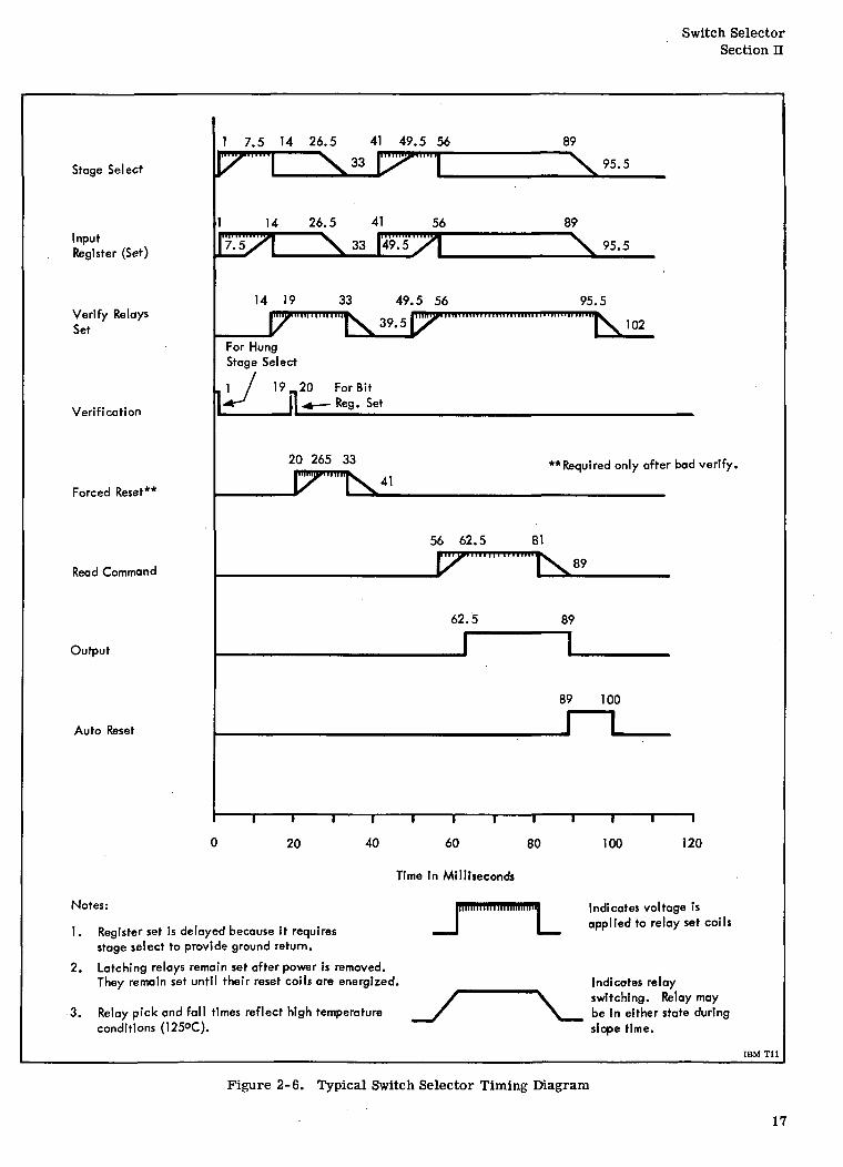
This section contains a more detailed des-cription of the Switch Selector. During this discus-sion, reference will be made to the timing diagram,Figure 2-6, the simplified schematic diagrams,Figures 2-7 through 2-15, and to the detailedschematic diagram, Figure 2-16.
16
Switch SelectorSection n
Stage Select
InputRegister (Set)
Verify RelaysSet
Verification
Forced Reset**
Read Command
Output
Auto Reset
Notes:
1 7.5 14 26.5 41 49.5 56 89
95.5
1 14 26.5 41 56 89
33 49. 95.5
14 19 33 49.5 56
IZ IX39-5195.5
For HungStage Select
1 / 19 20 For BitReg. Set
20 265 33 "Required only after bad verify.
56 62.5 81
IV89
62.5 89
89 100
i i I i i I i
20 40 60 80
Time In Milliseconds
I I
100 120
Indicates voltage Is
1. Register set is delayed because it requiresstage select to provide ground return.
2. Latching relays remain set after power Is removed.They remain set until their reset coils are energized.
3. Relay pick and fall times reflect high temperature /conditions (125°C).
JMiiiiiiuiiiiiiiiNimii indicates voltage is
I applied to relay set coils
Indicates relayswitching. Relay maybe In either state duringslope time.
IBM Til
Figure 2-6. Typical Switch Selector Timing Diagram
17
Switch SelectorSection n
2-5 STAGE SELECT
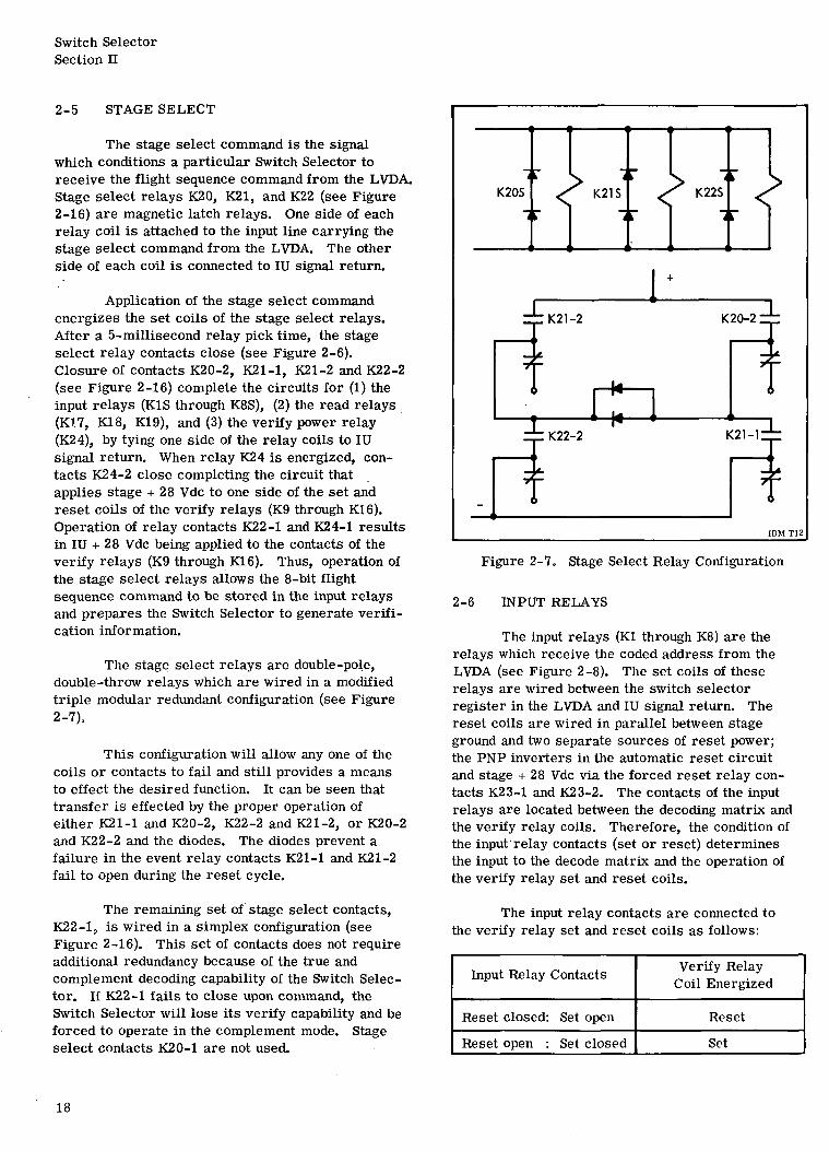
The stage select command is the signalwhich conditions a particular Switch Selector toreceive the flight sequence command from the LVDA.Stage select relays K20, K21, and K22 (see Figure2-16) are magnetic latch relays. One side of eachrelay coil is attached to the input line carrying thestage select command from the LVDA. The otherside of each coil is connected to IU signal return.
Application of the stage select commandenergizes the set coils of the stage select relays.After a 5-millisecond relay pick time, the stageselect relay contacts close (see Figure 2-6).Closure of contacts K20-2, K21-1, K21-2 and K22-2(see Figure 2-16) complete the circuits for (1) theinput relays (K1S through K8S), (2) the read relays(K1.7, K18, K19), and (3) the verify power relay(K24), by tying one side of the relay coils to IUsignal return. When relay K24 is energized, con-tacts K24-2 close completing the circuit thatapplies stage + 28 Vdc to one side of the set andreset coils of the verify relays (K9 through K16).Operation of relay contacts K22-1 and K24-1 resultsin IU + 28 Vdc being applied to the contacts of theverify relays (K9 through K16). Thus, operation ofthe stage select relays allows the 8-bit flightsequence command to be stored in the input relaysand prepares the Switch Selector to generate verifi-cation information.
The stage select relays are double-pole,double-throw relays which are wired in a modifiedtriple modular redundant configuration (see Figure2-7).
This configuration will allow any one of thecoils or contacts to fail and still provides a meansto effect the desired function. It can be seen thattransfer is effected by the proper operation ofeither K21-1 and K20-2, K22-2 and K21-2, or K20-2and K22-2 and the diodes. The diodes prevent afailure in the event relay contacts K21-1 and K21-2fail to open during the reset cycle.
The remaining set of stage select contacts,K22-1, is wired in a simplex configuration (seeFigure 2-16). This set of contacts does not requireadditional redundancy because of the true andcomplement decoding capability of the Switch Selec-tor. If K22-1 fails to close upon command, theSwitch Selector will lose its verify capability and beforced to operate in the complement mode. Stageselect contacts K20-1 are not used.
K20S K21S K22S <X>
K21-2 K20-2
yt ?
(
K22-2 K21-1
yi
t.
iy
(
IBM T12
Figure 2-7. Stage Select Relay Configuration
2-6 INPUT RELAYS
The input relays (Kl through K8) are therelays which receive the coded address from theLVDA (see Figure 2-8). The set coils of theserelays are wired between the switch selectorregister in the LVDA and IU signal return. Thereset coils are wired in parallel between stageground and two separate sources of reset power;the PNP inverters in the automatic reset circuitand stage + 28 Vdc via the forced reset relay con-tacts K23-1 and K23-2. The contacts of the inputrelays are located between the decoding matrix andthe verify relay coils. Therefore, the condition ofthe input'relay contacts (set or reset) determinesthe input to the decode matrix and the operation ofthe verify relay set and reset coils.
The input relay contacts are connected tothe verify relay set and reset coils as follows:
Input Relay Contacts
Reset closed: Set open
Reset open : Set closed
Verify RelayCoil Energized
Reset
Set
18
Switch SelectorSection n
p8 8X <-
vO
.4- O X M .OO U O — O i— CMO "3J "5J O CS CM CN
r- i
1I <
zv^
1 I**
«••••• ••••••) •••••• BBBBBBI ••••••> •••••• ^HM
1
• rt.^ °° <£K 9^^ cs <
0£
/\SV^
, » \
f f* i' *1 ,
K
v"
J
••••• BB^BBB •••••••) BBB^H
™ " |
fc.CO 10 ^
oo
^v^Id Ur P
t
i
r ii
* ac- *
'
s;
V \f f
i
1" 11
6u
ffii—D-
z
0 J2 CNT J 0 1
a. e xTg) _ o co
.*_ — J2 o— *- ^ 4>CO ID C —
O 0 C O1- Q£ 0 Q.
Q00
00CN
Q i >
toK
)S <
00CO
Q 0
.0 v£ CNc i
212
VQA1 u10^ uo|4Diiuoju( 4ndu[ 1
Figure 2-8. Input and Verify Relay Circuitry
19
Switch SelectorSection II
The input relay contacts connect stageground to one side of either the set or reset coilsof the verify relays. This completes the circuitthrough the coils to stage + 28 Vdc, thereby pro-viding verification information to the LVDA. Inaddition, the input relay contacts determine how thebit and bit NOT input lines to the decode matrix areconditioned. The following table shows the relation-ship between the input relay contacts and the inputsto the decode matrix.
Input RelayContacts
Reset closed:Set open
Reset open:Set closed
BitFunction
Down level(0 Vdc)
Up level(+28 Vdc)
Bit NOTFunction
Up level(+28 Vdc)
Down level(0 Vdc)
A down level voltage is obtained on a decodematrix input line when that line is tied to stageground through the input relay contacts, and an uplevel voltage exists on the matrix input line which isnot tied to stage ground. In the event relay contactK24-2 fails to close, an open circuit at the input tothe decode matrix is considered to be an up levelvoltage.
It should be noted that the stage select com-mand and the coded input command are sent from theLVDA at the same time (see Figure 2-6). However,the input relays will not pick until a maximum of6. 5 milliseconds after the initiation of these signals.The delay is due to the pick time of the stage selectrelays. It then takes a maximum of 6. 5 millisecondsto pick the input relays. This means that after amaximum of 13 milliseconds after initial receipt ofthe stage select command, power will be applied tothe verify relay coils. The power is applied in sucha manner that the information contained in the veri-fy relay coils is the coded input command held inthe input relays.
The input relays are wired in a simplex con-figuration. Redundancy is provided by the true orcomplement decoding capability of the SwitchSelector.
Resetting of the input relays will be discuss-ed later under the headings RESET (FORCED) andRESET (AUTOMATIC).
2-7 VERIFICATION
Verification is the process by which theSwitch Selector automatically informs the LVDC(through the LVDA) that the correct input commandis stored in the input relays of the Switch Selector.
This process is controlled by the operationof the stage select and input relays (see Figure2-16). The stage select command results in stage+ 28 Vdc being applied to the set and reset coils ofthe verify relays (K9 through K16) and IU + 28 Vdcbeing applied to the normally closed verify relaycontacts (see paragraph 2-5, STAGE SELECT).The coded input address results in the input relaycontacts being set to reflect the input address.Upon successful acceptance of the stage select com-mand and the input address, the Switch Selector isfully conditioned to send verification information tothe LVDA.
The information sent to the LVDA is deter-mined by the condition of the input relay contacts(see Figure 2-8). When the input relay contactsare in the reset position, the verify relay resetcoils are energized and the verify relay contactsremain in their normally closed position. Whenthe input relay contacts are in the set position, theverify relay set coils are energized and the verifyrelay contacts are switched to the open position.
Thus, to energize the set coil of a verifyrelay, allowing no voltage to be sent to the LVDA,the corresponding input relay must be set, indicat-ing a binary "1" for that particular bit of the inputcommand. Conversely, to energize the reset coilof a verify relay, allowing + 28 Vdc to be sent tothe LVDA, the corresponding input relay must bereset, indicating a binary "0" for that particularbit of the input command. The verification outputis therefore the complement of the input command.
Power will be applied to the verification out-put circuitry a maximum of 13 milliseconds afterreceipt of the stage select command (see Figure2-6). However, the verification output for a giveninput command will not be present until a maximumof 18 milliseconds after the stage select commandhas been received. This is due to the relay picktimes of the stage select, input, and verify relays.
2-8 RESET (FORCED)
One conventional double-pole, double-throwrelay, K23, is used to control forced resetting of a
20
Switch SelectorSection II
Switch Selector (see Figure 2-16). The forcedreset command is issued only if a false verificationhas been received by the LVDC. When this occurs,it is necessary to clear the information stored inthe input relays in order to prepare them to receivethe complement of the original input command.
Forced reset is initiated upon receipt of thereset command from the LVDA. The reset com-mand is applied to one side of the reset relay coil,K23. The other side is connected to IU signalreturn. When the coil of K23 is energized, normal-ly open contacts K23-1 and K23-2 close, applyingstage + 28 Vdc to one side of the stage select relayreset coils (K20R through K22R), and to one side ofthe input relay reset coils (KIR through K8R). Sincerelays KIR through K8R and K20R through K22R havethe other side of their coils connected to stage ground,these relays will be reset. Series limiting resistorsR24-R34 protect the reset relay coils agains currentsurges.
Resetting of the stage select and input relaysresults in stage ground being applied to the verifyrelay reset coils K9R through K16R, and power beingremoved from verify power relay K24. Under theseconditions power will be applied to the verify relayreset coils for a period of time equal to the relay falltime of K24. During this time, the verify relays (K9through K16) will be reset. The Switch Selector isnow reset and ready to receive the complement of theoriginal command. The reset cycle is completed19. 5 milliseconds after application of the forcedreset command (see Figure 2-6).
When the read relays are energized, thenormally open contacts of K17-1, K18-1, K18-2,and K19-1 close resulting in stage ground beingapplied to the base circuits of the switch powerinverters (SPWRA and SPWRC) in the AG portion ofthe decode matrix. This allows the decoding pro-cess to take place and an output to be generated.The Switch Selector output is present a maximum of6. 5 milliseconds after receipt of the read commandand remains until the read command is removedand the read command contacts open (see Figure2-6).
The read relays are wired in a modifiedtriple modular redundant configuration (see Figure2-9). This configuration allows any one of the coilsor contacts to fail and still provides a means bywhich the desired function can be accomplished. Itcan be seen that transfer is effected by the properoperation of either K18-2 and K19-1, K17-1 andK18-1, or K17-1 and K19-2 and the diodes. Thediodes prevent a failure in the event relay contactsK18-1 and K18-2 remain closed after the read com-mand has been removed.
Read relay contacts K17-2 and K19-2 areused to control the automatic reset circuitry. Theautomatic reset function will be discussed in thefollowing paragraph.
2-10 RESET (AUTOMATIC)
Automatic reset is accomplished by a pulsegenerated within the Switch Selector. The pulse is
2-9 READ COMMAND
The read command initiates two separatefunctions in the Switch Selector. First, the readcommand enables the decode matrix, allowing anoutput to be generated. Second, the read commandinitiates the automatic reset cycle.
Three conventional relays, K17 through K19,receive the read command from the LVDA (seeFigure 2-16). One side of the relay coils is con-nected to the read command signal; the other sideof the coils is tied to IU signal return through stageselect relay contacts K20-2, K21-1, K21-2 andK22-2. Because the read command relays are con-nected to IU signal return through the stage selectrelays, it can be seen that a stage select commandmust be received by the Switch Selector before aread command can be accepted.
KI7-I
To StageGround
K18-1
K18-2
To SwitchPower Inverters,SPWRA and SPWRC
KI9-I
Figure 2-9. Read Command Relay Configuration
21
Switch SelectorSection II
initiated by operation of read command relay con-tacts K17-2 and K19-2 and accomplishes the samefunction as the forced reset.
A series-parallel network of capacitors,Cl through C26, is connected as shown in Figure2-10. One side of the network is tied to stageground; the other side is connected to read commandrelay contacts K17-2 and K19-2. When these con-tacts are in their normally closed position, thecapacitor network is connected through four parallelthermistors, RT1 through RT4, to the base circuits(A) of three parallel PNP inverters (IpLc). (Seeparagraph 2-14 for a description of the invertercircuit.) If the capacitors are discharged, the in-verters will be activated causing the output (B) to go
to approximately stage +28 Vdc. This conditionallows the capacitors to charge to stage + 28 Vdcpresent at the gated input (C) of the inverters. Thecharge path is through the transistor, transistor baseresistor, and the thermistors. The charge time isdetermined by the equivalent value of these resist-ances and the equivalent value of the capacitance ofthe capacitor network. When the capacitors havecharged to a voltage equivalent to that needed to shutoff the inverter, the voltage at B drops to 0 Vdc. Thepulse thus generated at B of the inverters is theautomatic reset pulse. These pulses are connectedto reset coils KIR through K8R and K20R throughK22R through series limiting resistors R5 throughRl 5. The pulse width is equivalent to the time be-tween turn ON and turn OFF of the inverters.
Stage +28 Vdc
Note: Relay contacts shownIn their normally closedposition.
To Stage Select Reset CollsK20R, K21R, K22R
To Bit 8 Reset CollKIR
To Bit 7 Reset CollK2R
To Bit 6 Reset CollK3R
To Bit 5 Reset CoilK4R
To Bit 4 Reset CoilK5R
To Bit 3 Reset CoilK6R
To Bit 2 Reset CollK7R
To Bit I Reset CollK8R
1111111111111
>B!t RelayReset Coils
C13
ST* '"T^ ST* ^T^ XTN «qN ^TN ^T\ /TN ^T\ ^TN XTN /TN
Rl R2 R3 R4•*• To Stage Gnd
IBM T15
Figure 2-10. Automatic Reset Circuitry
22
Switch SelectorSection n
The capacitor network is discharged throughresistors Rl through R4 during the read command.When relay contacts K17-2 and K19-2 close, thehigh side of the capacitor network is connected toone side of the resistor network. The other side ofthe resistor network is tied to stage ground. Thedischarge time is determined by the RC time con-stant of the equivalent resistance of the resistornetwork and the equivalent capacitance of the capac-itor network.
Because the output of the inverters (B) mayvary with temperature, 4 thermistors, RT1 throughRT4, were placed in the base circuits of the in-verters. The thermistors compensate for outputvariations due to temperature change by adding orreducing resistance in the base circuit, therebyincreasing or decreasing the base drive of the cir-cuit as necessary. The effect of this compensationis to maintain a constant charge time and therebymaintain the width of the automatic reset pulse with-in the allowable design range of 3-1/2 to 12 milli-seconds. The RC charge time determines the timeduration between turn ON and turn OFF of the invert-ers.
The capacitor network was purposely madelarge so that a failure of one capacitor within thenetwork can be tolerated without the automatic resetpulse width being forced out of tolerance, causingthe Switch Selector to fail.
The automatic reset pulse commences 8milliseconds after the read command has been re-moved (see Figure 2-6). This is due to the timerequired for the contacts of read command relaysK17-2 and K19-2 to return to their normally closedpositions.
2-11 DECODING MATRIX
The decoding matrix is comprised of PNPinverters, NPN inverters, and AND logic circuits(see paragraph 2-14 for description of electroniccircuits). The circuits are arranged so that the in-put address can be decoded in either its true orcomplement form.
The output matrix is divided into threesections as follows:
AG generation logic
Row logic
Column logic
The object of these three sections is togenerate column and row signals for each inputcode and to transfer these signals to the output ma-trix upon receipt of the read command.
AG Generation Logic
The AND gate circuitry (see Figure 2-11)develops the control signals for the output section ofthe Switch Selector. These signals (AG1 throughAG5) are applied as gated inputs to the row andcolumn decoders, which in turn condition the outpu'matrix to produce the desired Switch Selector out-put.
Operation of the read command relays tiesthe inputs (A) of the switch power inverters to stageground, resulting in the generation of the SPWRAand SPWRC signals.
The output of the SPWRA inverter is sup-plied as the gated input to the PNP inverters (Ip_)that generate AG1 and AGIN signals. The binaryvalue of bit 8 of the input code determines whetherAG1 or AGIN is generated. Refer to paragraph 2-6,INPUT RELAYS, to determine the manner in whichthe input relays transfer the input code to thedecoding matrix.
If bit 8 (B8) is a binary "1", approximately+ 28 Vdc is applied to the input (A) of the IpL thatgenerates AGIN. Since the input is + 28 Vdc, theinverter is turned OFF and the output (B) will be 0Vdc, thus AGIN is a binary "0". If bit 8 (B8) is abinary "1", bit 8 NOT (B8N) is a binary "0" placing0 Vdc on the input (A) of the inverter that generatesAG1. With the input of the inverter at 0 Vdc, theinverter is turned ON and the output (B) will be+ 28 Vdc, thus AG1 is a binary "1".
If the binary values of B8 and B8N arereversed, the inverter action described above willbe reversed and the binary value of the AGl signalswill be reversed.
The AGl and AGIN signals are sent to otherIpL's to Senera-te the AG2 through AG5 signals.The AGl signal is applied as the gated input to theIPL's that generate the AG2 and AG3 signals. TheAGIN signal is applied as the gated input to theIpL's generating AG4 and AG5 signals. Therefore,regardless of the binary value of B8 of the inputcode, two of the four inverters that generate AG2,AG3, AG4, and AG5 are supplied with a gated input.
23
Switch SelectorSection n
(
1
£gacc
4-V
£
coCO
)»1
>
o . .
11h
CM
O
CO
1 — u *"
s
21I/I
CO
O — '
<~t > 7
i TOQ
y '- u ^ -,<
«A
*l ui)| O)"O
y
mO<
z
<
<
5CO
a
^
t
— CM COjs -^r ^- ^~Q U U U
vHH^e-
co o- oO CO CO "3"0 O U O
Mneie
o5 O)
0 0 0H- °£ — '
coo<
0 _ CO
<I U c^
t <
i--CO
__ zO O i -i< <]
J _... U n"1
< <
Z co
CO
M f5 J J1 . 1 i- §•I . E E1 III 2 *- 2 u
1 1 u_ Ji u_ 3-
<aP
u aro
^ OJUJ
n ( i
3<•— CO
o<
<
K1 CO
1 1 1 '
O O+- •*-D DCL ,. Q. t.c <u c ;;
K ll)^ ifCQ <-H >- ca «i" L.
zO -v
3
2 £1
O ,
5 fe eot la;i^ — >
£ 0.
Figure 2-11. AG Signal Generation Logic
24
Switch SelectorSection n
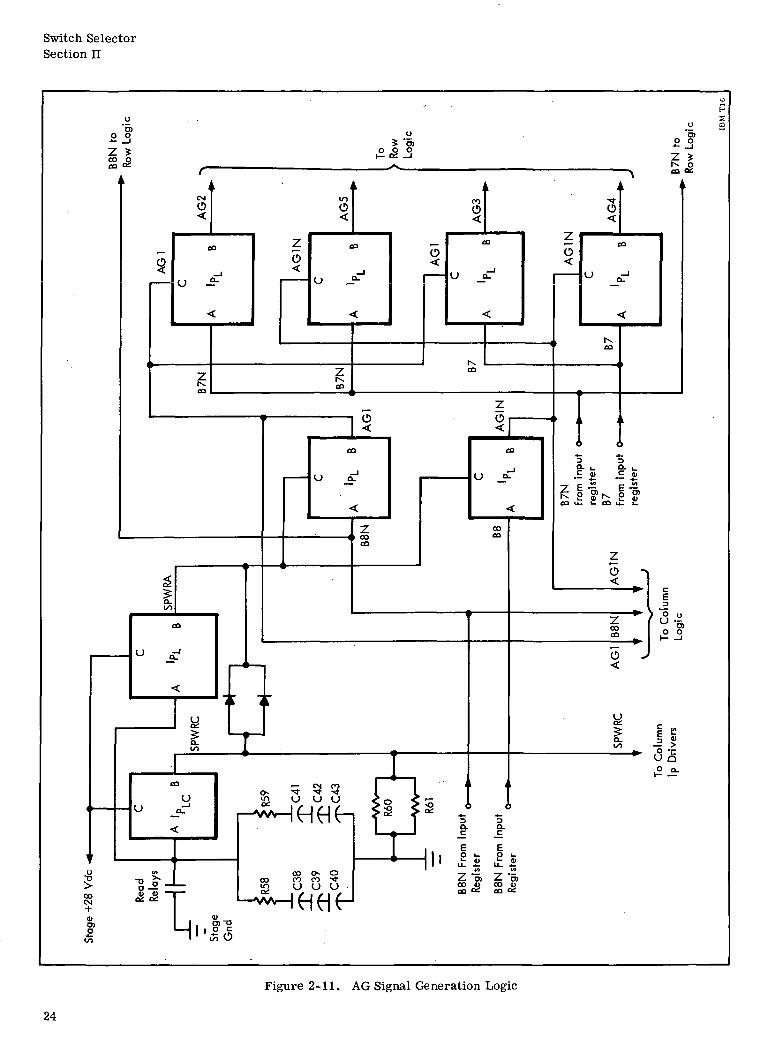
However, it is the binary value of B7 that deter-mines which of the inverters supplied with a gatedinput is activated,
When B7 is a binary "1" and AG1 is present,+ 28 Vdc is applied to the input (A) of the inverterthat generates AG3. This signal (+ 28 Vdc) main-tains the AG3 inverter in the OFF state makingAG3 a binary "0". However, under these same con-ditions, B7N is a binary "0". When this signal(0 Vdc) is applied to the input of the AG2 inverter,the inverter is activated making AG2 a binary "1".
If the binary value of B7 is zero, the inverteraction described above will be reversed making AG2a binary "0" and AG3 a binary "1".
If B7 is a binary "0" and AGIN is present,the above description will be true for the invertersgenerating AG4 and AG5 signals. The AG2, AG3,AG4, and AG5 signals are applied as gated inputsto the AND gates in the logic circuits developing therow NOT signals.
SPWRC is applied to the column Ip driversapproximately 300 microseconds after the generationof the AG signals, thereby allowing the row andcolumn logic to be conditioned before the column Ipdrivers are conditioned. This delay prevents thepossible generation of extraneous Switch Selectoroutputs. The time delay is accomplished by install-ing a 0. 82 microfarad capacitor between the baseand emitter of each transistor in the SPWRC invert-er.
The filter circuit (R58, R59 and C38-C43) on ,the input of the switch power inverters serves toreduce 28 volt fluctuations caused by chatter in theread relays. The filter causes the SPWRA andSPWRC signals to rise more smoothly, therebypreventing the possibility of voltage spikes beingcoupled to the output logic causing extraneousSwitch Selector outputs.
The purpose of the diodes located betweenSPWRA and SPWRC is to make the turn off time ofSPWRC inverter equal to the turn off time of SPWRAinverter. (SPWRC will lag SPWRA because of thecapacitors on the input of the SPWRC inverter.) IfSPWRC is allowed to lag SPWRA, the column Ipdrivers will remain gated once the SPWRA signal isremoved; making it possible to energize the NPNinverters in the column logic producing extraneousSwitch Selector outputs. In addition to the diodes,
resistors R60 and R61 serve as line dischargeresistors for SPWRC voltage.
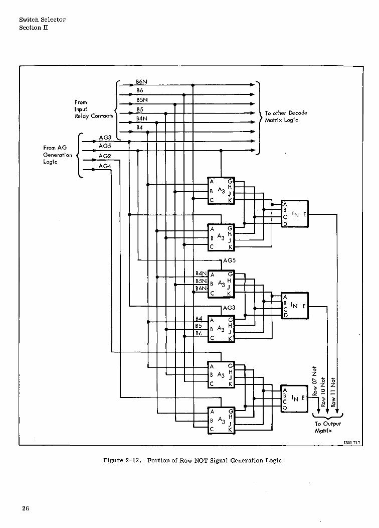
Row Logic
There are 16 row NOT signals generated. Aportion of the generation of these signals is shown inFigure 2-12. Each row NOT signal is generated bya pair of AND gates and a NPN inverter. The ANDgates sense either the true or complement code ofbits 4, 5, and 6. The code of bits 7 and 8 havepreviously been determined by generation of the AGsignal. Only one of the two AND gates can be quali-fied at one time, and that particular AND gate thenactivates the inverter which generates the desiredrow NOT signal.
As an example, the following discussion willshow how the row 10 NOT signal is generated. (Rowsignals are designated in octal.) The bottom ANDgate in the row 10 NOT circuitry has the AG3 signalas its gated supply. The inputs to this AND gate areB4, B5, and B6. In order to qualify this AND gate,the AG3, B4, B5 and B6 lines must all be at an uplevel. This requires that bits 4, 5, 6, 7 and 8 havethe following binary values:
B4, B5, B6 = Binary "1"
B7 = Binary "0"
B8 = Binary "1"
When the input code is as stated above, thebottom AND gate will be qualified producing an uplevel voltage to the input of the NPN inverter. Withan up level on the input, the output of the inverterwill be clamped to ground producing a row 10 NOTsignal.
If the verification shows an error, the comple-ment of the input code will be sent to the Switch Selec-tor.
The combination of B7 and B8 now combine toproduce an AG5 signal. B4, B5, and B6 are in a downlevel condition, resulting in the B4N, B5N and B6Nlines to the AND gate being conditioned at an up level.Thus, the inputs to the top AND gate in the row 10NOT circuitry are all up level producing an up levelinput to the NPN inverter. The up level on the inputof the inverter causes the output of the inverter to beclamped to stage ground producing a row 10 NOTsignal. Thus, a failure in the input relays can betolerated without generating an erroneous row NOTsignal thereby causing a Switch Selector failure.
25
Switch SelectorSection II
B6N
From AGGeneration <Logic
>mut ^ay Contacts
o AG3 s
B6
B5N
r B5
B4N
B4
AG5
r AG2
^ AG4
A
B A
r
A
B A
r
B4NB5NB6N
B4B5B6
A
GH
3 J
G
' • ?
To other Decode/ Matrix Logic
AG5
G
B A, H
C
A
B A
r
A
B A
r
A
B A
C
0 JK
AG3
G
3 ?
G
3 jK
G
V
^— IA
— D
B IM c_ c ri L— D
t5
fe o o, ° -r %
A | oB 1 c "^ "~I
— c I *D 1 , , ,
To Outpi
IBM T17
Figure 2-12. Portion of Row NOT Signal Generation Logic
26
Switch SelectorSection n
Each row NOT signal is generated in the samemanner, using different AG signals in conjunctionwith different combinations of B4, B5, B6, B4N,B5N, and B6N covering all possible input conditionsallowed. The row NOT signals are fed directly to theoutput matrix logic.
Column Logic
In addition to the row NOT signals, there areseven column signals generated in the decodingmatrix. Figure 2-13 illustrates a portion of thecolumn signal generation logic. These signals aregenerated in a manner similar to the row NOT sig-nals. Two AND gates, one NPN inverter, and onePNP inverter are used to produce the column signalwhich is fed directly to the output matrix logic. Thedifference stems from the use of different AG signals,different input signals, and an additional inverter(PNP type). The bias gating signals used in thecolumn circuitry are AG1 and AGIN, and the inputsignals are Bl, B2, B3, BIN, B2N and B3N. Theadditional inverter in the column circuitry resultsin the generated column signal being an up levelsignal, whereas the row NOT signal is a down levelsignal.
2-12 OUTPUT MATRIX AND TELEMETRY
Output Matrix
The output matrix consists of 112 PNP in-verters (Ip's) arranged in a 16 row by 17 columnmatrix (see Figure 2-16). Each allowed input com-mand will select 1 of the 112 Ip's and produce aSwitch Selector output. Each row NOT signal fromthe row logic is connected to the base input (A) ofseven output Ip's. Likewise, each column signalfrom the column logic is connected to the gated input(C) of 16 output Ip's.
Control of any 1 of the 112 output drivers isaccomplished as follows: An output driver is con-ditioned for an up level output (+28 Vdc) by thepresence of a down level (0 Vdc) at the base input andan up level at the gated input. These input conditionscause the PNP transistors in the selected Ip to con-duct, causing the +28 Vdc gated input to appear acrossthe output of the Ip. All other input conditions causethe Ip drivers to remain off, resulting in a downlevel output.
Thus, an up level voltage on the column lineand a down level voltage on the row NOT line willcause the output driver at the intersection of these
two lines to be at an up level voltage. All remainingoutput drivers will remain in the down level stage asconditioned by their inputs.
Telemetry
The PNP inverters used in the output matrixare modified to provide a special telemetry output(see Figure 2-18). The outputs are connectedto a common telemetry line and sent to stage telemetry(see Figure 2-16). An up level on any one of the out-put drivers results in an up level telemetry signal,indicating to the ground equipment the presence of aSwitch Selector output. The magnitude of the teleme-try signal is determined by a resistive network. Thetelemetry signals of 8 Ip's are connected through one12K resistor to stage ground. Therefore, theeffective telemetry resistance is the equivalent offourteen 12K resistors in parallel, or approximately806 ohms.
2-13 TEST OUTPUTS
The Switch Selector has two telemetry outputswhich are used to verify that the input selectionrelays can be set and reset properly. These signals,zero indicate and register test, are special outputsof the output matrix.
Zero Indicate
The presence of an all zero binary inputcommand results in an up level voltage at the zeroindicate output (see Figure 2-14). The Ip that pro-duces the zero indicate signal is conditioned at itsgated input (C) by three series connected logicelements; a four input AND gate (A4), a NPN inverter(IN), and a PNP inverter (IPL). An all zero inputcode yields an up level voltage output from the ANDgate. This up level is applied to the input of the NPNinverter resulting in its output being clamped toground. The down level NPN inverter output isapplied to the base input (A) of the PNP inverterresulting in an up level output. This up level be-comes the gated input for the zero indicate Ip.
The input (A) of the zero indicate (Ip) is con-ditioned by two series connected logic elements; afive input AND gate (As) and an NPN inverter. Theall zero input code causes an up level AND gate out-put which when applied to the NPN inverter, resultsin a down level inverter output. This down level isthe input (A) of the zero indicate Ip driver.
27
Switch SelectorSection n
,- B3N
FromInputRelay Contacts
From AGGeneration <
Logic
Jsets
31
Jl
1
, I( £
+1
N
1
S3
12N
12
UN
H
\ \ \
i
i
B AL
AR Af
A
B A
c
o Ab "r
A
R A
R AC
GII
3 ,
K
G
3 tiI
GLJ
•JK
Go HJ ,j
K
G• I
3JK
G
0
K
_ |
SPWRC
-A c
- B 1, , r A 1 n
D
SPWRC
>-A C
C N E A PL B
— D
SPWRC
-A c
n ili i r -• - A 'D E -.
D
8 S
II\ ' \
oc
3
OOi
To other Decode Matrix Logic To OutputMatrix
IBM TIB
Figure 2-13. Portion of Column Signal Generation Logic
28
The up level gated input, and the down levelbase input maintain the zero indicate Ip at an uplevel state. Conversely, during non-zero inputcodes, the zero indicate Ip is maintained at a downlevel output. Note that the read command is notrequired for zero indicate.
Register Test
The presence of all ones in the input code andthe application of the read command results in an uplevel voltage at the register test output (see Figure2-15). Similar to zero indicate, the register testIp is conditioned at the gated input (C) by threeseries logic elements; a three input AND gate (As),an IN inverter, and an Ip inverter. The input (A) is
Switch SelectorSection n
conditioned by two series connected logic elements;a three input AND gate (A^), and an IN inverter.This operation requires that the read command beissued. The read command initiates generation ofthe AG1 and AG2 gates. The AG1 and AG2 signalscondition the AND gates that generate the signalswhich are supplied to the gated input (C) and base in-put (A) of the register test (Ip). Conversely, duringthe all zero input code, the register test Ip maintainsa down level output.
2-14 CIRCUIT DESCRIPTION
This section contains a description of the cir-cuits and relays which make up the modules used inthe Switch Selector. The Switch Selector uses three
FromInput >Relay ]Contacts
From AGGenerationLogic
B4N
" B5N•" B6N
B8N
B7N
B4
B5
DO
w
AG2
!
B8N
BIN
B2N0-3MDOIN
y\
C .A
F
R /
fcA4
(
cJ
n3
G
j
K
3
G
•(•B
A
r1!h
. p4 L
Stag
'N
e+28
E
3 Vdc
PL
BoIn
sepu
GatedInput
C ZeroIndicate
t
IBM T19
Figure 2-14. Zero Indicate Logic
29
Switch SelectorSection H
basic logic circuits whose functions are AND andINVERT. There are two different types of inverters,one type uses PNP transistors and is designated Ip,the other type uses NPN transistors and is designatedIN-
AND Circuit
Logical operation of the AND circuit is asfollows: With an up level (+ 28 Vdc) on the gated in-put, and an up level on all of the remaining inputs,the AND circuit produces an up level output. A downlevel voltage (0 Vdc) at any of the AND circuit inputs,including the gated input, forces the output of the ANDcircuit to be clamped to the down level input.
The passive AND gate may have from four(A4) to six (Ae) inputs. The gated input for an ANDcircuit may be supplied directly from a + 28 Vdcsource, or by a + 28 Vdc signal from a PNP inverter.
The AND circuits have a quad-redundant configura-tion (see Figure 2-17 for an example of a quad-redundant four input AND circuit). Operation of anAND circuit will not be affected by the malfunction ofany detail part in the circuit.
PNP Inverter (Ip)
The Ip inverter uses four transistors to pro-vide a quad-redundant configuration (see Figure 2-18).Operation of the inverter will not be affected by themalfunction of any detail part in the circuit. Thegated input may be supplied directly from a + 28 Vdcsource or by a + 28 Vdc signal from a proceedingIp circuit.
FromInputRelay 'Contacts
From AGGenerationLogic
FromInputRelayContacts
B4N
B5N
B6N
B8N
B7N
i
B4
B5
B6>
AG2
A
;
D
G
J
K
A
B ;
C
G
^3 H
K
Q
' 'N E
, D
AG1
Bl
B2
B3
SPWRC
GHJ
K
A
B IC N
D
A 'PL B
BaseInput
GatedInput
RegisterTest
IBM T20
Figure 2-15. Register Test Logic
30
Switch SelectorSection n
Jl-A IU-26VDCJ4-A
Is 1 I 1 S s 1is 2|J l\i ±1 -p' ^ *•* *
CHASSISCND
F TLyx i s«™
K9 K10 Kll K12 K13 KM K15 K16"-V *-V i_L* i_Lt i_^ t_ t t_ t C. £.< F Y i i i i i f f i
VERIFY OUTPUTS
J1-W.X RESET
J1-H.J SIGNALJ4-H.J RETURN
CHASSISCNO
T/P
-1 ARSTI
J4-UV COMMAND
:OL2Jl-K BIT B(MSD1 ^. ,. _MSJ4.K »(--J
Jl-l BIT 7J4-L
C14IIIIIIIIIIIII (*-' •.** ^.^..^..^.^.^.^r.^^^..^..^^^.1
T T T T
J1-P BIT 'J4.P
£* J!LJ *_*. "«
Jt-T »T 1 (ISO) „
». 1- CIRCUIT xocuFitt) KTA 0.82 WF CAPACITOR 20.ip CIRCUIT wODimo 8» THE ELIMINATION
COtWtfatO FROM THE BASE TO EMITTER OF Of BAS£ ISOLATION DOOESCR1.CR2.CUEACH TRANSISTOR. AND CM
IBM T21 -1
Figure 2-16. Switch Selector Electrical Schematic Diagram (Sheet 1 of 2)
31/32
Switch SelectorSection n
B6N
8C
C 'H'J 'K '
AH
El
Gf— - - -
i - A
- A
'
P f
- A
-A
V*
L A
Xf— — —
L- A
B6B5N
C
--,A f
c -
K- -
AG2 i -
c -*
K
8*3 «:iC l< - -
JAG2 -A * G J
B A3 H
' 1
A F C -
' Ic K| —
c'P B 33100
pI
c
pJ
J
" BJTTs
c
i
c
_DjJ '
-f" • • -
* '!h
*
p «fc-P
COLUMN 0
C
-A lp
cf
00011A
cD11100
00010[A 1 Tj
' 'N £ —D11101
ir225-!'"cB 'N £ "j11110 e i
B -
ii
1
J
COLUMN 02
C
-A lp
p'fti
]
COLUMN 03
1C
' fCOLUMN 04
C
-A 'P
0•Ss
J
COLUMN osTc
- A 'p
— ?
B3¥s
COLUMN 06
C
-A lp
' ?
B^COLUMN 07
C
-A lp
P
•a*
T/P
F
illlp?C
ITH-- ,
UC2 _ _
, B A
A f (
B A3
C
4
4
. -
_ c
H 'Je
]AC4
6 * 3 H ~ ~J
B*3
i
c-A lp B
P
*8J3^EE ~*
" I
C
-A 'p B
pjfa -'
f
1<!
D
96J3-V
T" C
-A 'P IJ2-MM"*
1
1C
-A lp B
I (J
ar. "*
-A lp B ib-»•
C-l. Ip B
— f
JH *
C
I
c
pI
c
— p1c --
J3-Y
{
JC
— p
clp g 102
'" *&**—P
1
--
cv IP
D'ft
001 IPAB IND
11001
OW01
A
f 'N5
E —
11010
A
c 'NJ T
E -
11011 £
I
* •
- C
'pD•^
£.
C
P
U
i .
T
-(. -
i 'rD
iia.J2-
Tcc
-C
h 'P
1
Bfe:
-C
k lp
1
s!lrp. -
4 .
-C
'P
P.
5§TZ L
C
A P
T/P
T/P
p
QC£a
B
_D.
PC
J2-W
T
C
A lp
1i
B
_0.ST. -'P
T
-4
c
tC
A 'P
1
A IP
T
B
D
cU2- -A IPJ3-z . I
T
B
-f
c
— ]
C
r-4A lp
B
Cffl- -A lpJ3-L
i •
B
D
0 °3 j . _
-C K- -
|AC3 -A F CJ
• ACS
- C K- -
|AG3 -A F C J
B 3 j
- - C K
AC4A F G-
1 6*3 H —
Me K —
. TC
B^ f r r ' -A 'P B
p Di
- n QtOOl
— :1B N C
5
10110
T ^ OtOOO
10111
,._
11000 §5! '
111I
J2T<
T
= ^r. - * ' P BD p, {
ih
tC
r ' — f32 .
1
Tc
-4-
it
*&, -*» B3-M
t
i" ' r%j
CEfreB * 'p B
r^ " —9-
u.3-KK
TC
-A 'P ETT- -A
D
tC
- * ' P .ft; - '
r
Jd
^3-H
Tc
01
Tc
_A lp BJJT^H - A '
— rf c
_ A - ' p B J^ -A
| fj l_
- A . p . f c L 4 , f
0
C K - -
,p A, h
_ C K
JAC5
8 *3 5 -^
i C K
,
li|iL|« '3 »[=
"— >..n A H - —
1 B A3 H —
' ]C K
TC
p Brf- -A 'P BD pi [
J IN E3
10011
— I 01 onV
> IN E
5
T,
10100
— T10501 og
B4
T: c
P D
1 1
T: c
_D_ "* D
I: t -P »ffe -A '" B
D p| 1
: c
-fT^ . L- ffe
» fc
f LLpJ-S-
> •H \rf-\
D D ^K
il
i
1
C-A lp *1
n
C
j j - A I P
1
Tc
— A 'P
D
c
Tc
T
" j
^
c
tc
Tc
•-c
t-c
B fi
c
rLT
D
ir-K -A P1 ,
B fP
C
r
D
C
^ IAC5
i C K -
A .* C
B 3 j
B A3 j~^
, C K--
JAC3 -
8*3 j
C K
Ucs
B A3 H —
B i|- ' - A l p B
p D
1
CIRCUIT SCHEMA!A
GATE INPUTO— «
- - E
- -C
IN E
T/P
10000
- -. 01110- f
• - -E 'N E
T/
10001
1
51101
'N E
10010
-ffc,
Tc
8 jfl - * 'P B
" 9I
13J2T.
cB J3_p - A lp B
^
T
•SV-** B
' pIft*
t
B ^ - A ^ P B
r1 ' 1 — FSfc
C
D}fc
• ..
i rnB5b L» 'p B 104.
3-i
>-^r-ii — w\ — 4
R36i WV— t
S37 !
. j STACE CNO
T/P
ii
il
(.
|C
— A 'P
1C
1C
-A IP
1
P1
•!n1
B 2
B ?pI
-A 'P BJ
1 ^J
C-A Ip
C
•3-
p
Co .- HDo f- HEo — «- M
Hr~ALL DIODES ARE S1N645
H !M— <
- -K —
~tr~!- -M —- M
M —
M
ICS
* * >T o 1
1,«« W o
IHK '
L>f '» K K
°'N
E
IN ^OUTPUT
SIN753A S2N22^J/7^2222 SIN75JA
i
1
ST.
ifl_
i3-E
A.2-AA
4_
b
TH
SIN753A S2N22
c° @ 1 (\
BASE INPUT
3K
2
F
3K >
^2222 SIN753A
'p
9GATED
7.5 K > f-^ LJ-,
CR3^ vb/ \dS2N2907J |S2
7.5K >2*
1 »- W-i ^CR5 S2N25
AIL DIODES ABE S
NOTES:1. TERMINALS
CIRCUITS2. ALL Ip
4. ALL RELAY
S. CASE GRC
6. R1-R4=682. R5-R15.R5S. P.16-R34.R9. C27-C34.
10. R35- R48=11. R49-
12. ALL DIODE13. 2ENER OK
14. K1-16.K20-
16.C1-C26.C3617.R60-R61 =18. RT1-RT4-= f
TELEMETRY* • -J2-G
071
; ICR? s
4
N645 "CR8J
E
E1.F AS SMC
SESPECTIVELY.
CIRCUITS Af
(CUltS ARE N
CONTACTS SH
UND J l - j
J2-
J3-
J4-I
)^.1/8W 4on
SO-R57-270A.CAPACITOR F£EC2K 1/8W 606100.H..3W 60!S<S1N645 40
JDES-SIN753A
22 • FL4068.724- FC4073.6
-C43 = SORAC
EYSTONE Ri4
3K > 6 l2V
INPUT
2K>> 7.5K
) — *-*S*A> — »/ CR
2I<S 7.5K
) — l-w\, — •*•' CR1*22Q2<J OUTPUT
!CR9 6
> 10K>I — oTELlMETRY
D
WN ABOVE, OF ALL lp
1RECONNECTEDTOSTAGLE CLAMPID TO STAGEOT CLAMPED TO STAGEOWN AS RESET
Pp
8W 401208!3W 6082084
1THROUGH FIlTER (08J«!0*808782090 '
40808*4
?5/l±5*/n AT 25 °C
30 A* 5 "feW ?5°C
JE-350D-0.6?MF±59
IBM
i CR2
4
6
UN
E GND
GND
CND
082078081071
T21-2
Figure 2-16. Switch Selector Electrical Schematic Diagram (Sheet 2 of 2)
33/34
Switch SelectorSection H
Logical operation of an Ip inverter is asfollows: An up level gated input (C) and a down levelbase input (A) causes the four PNP transistors tosaturate. The low collector to emitter impedance ofthe transistors allows the up level gated input to beseen at the output (B), resulting in an up level Ipoutput. All other inputs cause the transistor to havea high impedance from collector to emitter, main-taining the output of the Ip at a down level voltage.
The Ip inverters are used in the AG signalgeneration circuits, the decode matrix circuits, andthe output matrix circuits. The Ip circuits areclassified into three groups due to modification in theoutput circuits of the Ip's. See Figure 2-18.
Ip Driver - A telemetry output is coupled to the out-put of the Ip driver. An up level Ip output will resultin an up level telemetry output. One 12K telemetryload resistor is associated with each eight Ip drivercircuits. The output of the Ip driver is clamped tostage ground through two series diodes. The switchselector output matrix is made up of this type ofinverter.
IpL Driver (undamped) - The IpL inverter differsfrom the Ip inverter in that it has no telemetry out-put and the series clamping diodes have been removed.This type of inverter is used in the AG signal genera-tion circuitry and as column signal drivers.
Ip., p Driver - The !PLQ inverter differs from theIPL inverter in that the !PLC nas keen modified byinstalling a 0. 82 -microfarad capacitor in parallelwith the 2K resistor from the base to emitter ofeach transistor. This capacitance provides a 300-microsecond delay at the output of the IpL c« Theseinverters are used in the AG signal generation cir-cuitry and the automatic reset circuitry.
NPN Inverters (IN)
The IN inverter uses four quad- redundant NPNtransistors (see Figure 2-19). Operation of the in-verter will not be affected by the malfunction of anydetail part in the circuit. The 1^ inverter is pre-ceeded by a quad- redundant AND circuit and followedby an Ip inverter circuit. The bias voltages for theIJT inverters are obtained from the Ip inverterswhich they drive.
Logical operation of an IN inverter is asfollows: an up level input from the AND gate appliedto the bases of the NPN transistors will cause them toconduct, clamping the output at ground or down level.
A down level input will maintain the transistor in theOFF state and present a high-impedance output orup level to the following Ip circuit.
A Zener diode is provided on each input lineof the IN to ensure the transistors remain OFFwhen the output of the AND gate is at the down level.The Zener diodes prevent the NPN transistors frombeing turned ON by the voltage across the diodesin the AND gate.
Relays
The Switch Selector uses both latch and con-ventional type relays. Table 2-4 lists the SwitchSelector relay functions.
Latch Type - The latch type relay (see Figure 2-20)has two relay coils, K1S and KIR, associated witha pair of relay contacts, Kl-1 and Kl-2. The relaycontacts are controlled through the medium of amagnetic field and operate in unison. A pulse ofvoltage, of sufficient magnitude and duration,
Gate Inputo
Input A
Input B
Input C< -
l6K
-*
l6K
-H-
IBM T22
Figure 2-17. Four Input AND Circuit (A4)
35
Switch SelectorSection II
applied across a relay coil will cause the relay con-tacts to set or reset depending upon whether the set(KLS) or reset (KIR) coil is pulsed. The relay con-tacts will remain in the set or reset position afterexcitation is removed because of the latch capabilityof the relays. Transient suppressor diodes parallelthe coils. The maximum set and reset (pick and fall)time for latch type relays is 6.5 milliseconds athigh temperature conditions (125 °C).
Conventional Type - The conventional relay (seeFigure 2-21) has a single relay coil (K2) associatedwith a pair of relay contacts (K2-1 and K2-2). Thepair of relay contacts operate in unison. Excitationof the coil will cause the contacts to close; continuedexcitation is necessary for the contacts to remainclosed. When the excitation is removed, the contactswill return to the normally open position. Transientsuppressor diodes parallel the coils. The maximumpick time for the conventional type relay is fivemilliseconds, and the maximum fall time is 8 milli-seconds at high temperature conditions (125°C).
E Output
Stage Ground
Figure 2-19. NPN Inverter Schematic Diagram
A o-Base Input
0=82 mf capacitors on|p Inverters only
E
>10K
12K
>—WNr -O Telemetry
Stage Ground
•Telemetry OutputNot Used on lpj_and lp|_£ Inverters
IBM T23
Figure 2-18. PNP Inverter Schematic Diagram
36
Switch SelectorSection n
K1S
" HKl-l
KIR
:R
Kl-2
S
IBM T25
K2 9
- <K2-1
K2-2
IBM T26
Figure 2-21. Conventional Relay Schematic Diagram
Figure 2-20. Latching Relay Schematic Diagram
Table 2-1. Switch Selector Relay Functions
Relay
K1S
thru
K8S
KIRthruK8R
K9SthruK16S
K9RthruK16R
K17
K18
K19
Contacts
Kl-l, Kl-2
thru
K8-1, K8-2
Kl-l, Kl-2thru
K8-1, K8-2
K9thruK16
K9thruK16
K17-1
K17-2
K18-1K18-2
K19-1
K19-2
Function
Bit relay contacts - Used to store the flight command in the input register.Transfers command code to the AG and decode circuitry. Also applies powerto the proper verify relay coils allowing verification information to be returnedto the LVDA. These relays are magnetic latch relays.
Bit relay contacts are reset when KIR through K8R coils are energized,returning the input register to its reset condition.
When latch type relays K9S through K16S are energized, the NC verify relaycontacts, K9 through K16, are opened. This removes IU +28 Vdc from theverification lines going to the LVDA.
Verify relay reset relays. When the reset coils are energized, the verifycontacts K9 through K16 return to their NC position, applying IU +28 Vdcto the verification lines.
Read command relay contact K17- 1 is 1 of 4 sets of relay contacts which closewhen the read command is given applying stage +28 Vdc to the AG circuitry.
One of the three read command relays - When the read command is given,relay contact K17-2 closes initiating the automatic reset cycle.
Read command relay - When energized in conjunction with K17 and K19,K18-1 and K18-2 apply stage +28 Vdc to AG circuitry.
Read command relay - When energized in conjunction with K17 and K18,K19-1 applies stage +28 Vdc to the AG circuitry.
Same as K17-2.
37
Switch SelectorSection II
Table 2-4. Switch Selector Relay Functions (Cont)
Relay
K20S
K21S
K22S
K20R
thru
K22R
K23
K24
Contacts
K20-1
K20-2
K21-1K21-2
K22-1
K22-2
K20-1, K20-2
thru
K22-1, K22-2
K23-1, K23-2
K24-1K24-2
Function
Not used
One of the four sets of relay contacts required to complete the signal returnpath for the input relays (K1S through K8S) and the read command relays.Energized by the stage select commandoStage select relay - K21-1 and K21-2 are two of the four sets of contactsrequired to complete the signal return path for the input relays and the readcommand relays. This is a magnetic latching relay.
Stage select relay - One of the two sets of relay contacts which, uponapplication of the stage select command, applies IU + 28 Vdc to the verifyoutput relay contacts. This is a magnetic latching relay.
One of the four sets of contacts which, upon application of the stage selectcommand, completes the signal return path for the input relays and theread command relays.
Stage selet reset relays T - When K20R, K21R and K22R are energized,the noted relay contacts return to their normally open position therebyremoving the signal return path from the input relays and read commandrelay; removes stage +28 Vdc from the AG circuitry; and interrupts IU+28 Vdc to the verify output relay contacts.
Reset relay coil - Upon application of the reset command, stage +28 Vdcis applied, via K23-1 and K23-2, to the input relay reset coils and thestage select relay reset coils.
Verify power relay - This relay is energized upon closure of the stage selectcontacts completing IU signal return circuit, and applies IU +28 Vdc to theverify relay contacts and stage +28 Vdc to the verify relay coils.
2-15 REFERENCE MATERIAL
This section contains reference materialwhich will prove helpful to personnel involved introuble analysis of the Switch Selector. Figure 2-22(sheet 1 through sheet 6) is the complete logicdiagram for the Switch Selector. Figures 2-23through 2-38 are the electrical schematic diagramsfor the 16 different circuit modules used in ModelII Switch Selectors.
38
Switch SelectorSection II
STAGE.. „, xx E226JC_ SEIECT
J1 WX J4 WX « E'«C,D0 RESET
1 P19
|p,o TK2"5i
1 «",
IPS TK2^
BRTN
uL|P20 MCR18 P211
I ^434© J
I ^1
k *«4 -i A1A13VJJ1 6101434
MCR18 P271
SRTN
OE12ATP
"" P7 IARTN
U t"'2^ (6)
L A1A156101434
IPII I1* A **1 P»l
-p ^T^V4 '
JEUory i,jg2riT=iTMi«l- ^1 CRB CR»A1A13 (A) 1| 6101434^ |
]pn i~ A"I p». " K2SV
IP12rrn . /\K2R
4P22p=J4MV
wi PH i,L CR8- CR« A1A14 (5) I
6101434 |
1 CR7£_^TCR7 1
'Pll 1 A 1 P»J
I K2SV *
JP12[ R4 | A*'?B
1 a rm *n M* ^'CDS CR9A1A15 ©
6101434
Jl A Ji A « E«C.D0IU»2BVDC
11 i. i u 111 « E24K .JRET'URN
iui
STAGE COMMON
FRST _,SRTN (
ARST 1
n; i!p.2-8^-.lCR1CR2i;k 1i CR^f1 1
?10 AA16^
I 1 L^fHj
I /—I I P1«VFV
|_^i«J IPX)^"*-'* 11 ' [ A1A15 (6) ,
i 6101434 1Li» ^ . ^«J
JpTo " 1 ! | piijAVFY
i?.?r<Ji' ! i '-T^"0
i" < 1 A1AIA <^1 I' A1A9 © ' | 6101433 |
1 6101433 |
T
f~". "~~ . "~"~ "T" TlU*28VDC .
J I -Lc, 1|U»28VPC
I T« I1 1_ ^CHASSISCRD
| f ^ 1 *• 1 oSIQNAl RETURN ,
" " 1 1 T^1 i11 1 1 ISjCflAl. RETURN
, A2A11 .1 6082M4 1
PANEL A1A1®
61014(56
1 CR13 CR15~JF,RST 0|CIT VERIFICATION E4?C'D vv
| J-n3_r. '» ' "*>J1 i"J4 *>-
1— i — I -A1A16©!1 610143 3_|
I CR15. "^SECOND DIGIT VERIFICATION E26^27C vv .
iu-is; "7|o. -i- A1A15-© 1| 6101434 i
C^f^7 THI«P DIGIT VERIFI CATION "9C.D _
„ 3.,i ^7|— o£a — i IAIAM © '|_ 6101434 _J
I CR1L'CR£~1 FOURTH DIGIT VWIFICATION f^OfJJD
iK3-1± P 1iP3 T TAIAIT (6~) '| 6K)1434 |
1 C"« ^F'f'H O'C'T VERIFICATION ?33A* ,.,.,.
In T"4,,,, 1I 6101564 1
| CRU CRiriSIXTH 01QT VERIFICATION E"C.D vv
1 J-«u4' "*iP3 T T*IAII(^I| 6101541 |
I CR'i CRJ? ISEVENTH DIGIT VERIFICATION £3<>C.D „ . ,. h
L }"4mio i| 6101563^ |
1 CR1?. CR,i5 IEICHT DIGIT VERIFICATION ^9CD ^ ,. . ., .
. il , J, 7l6l " *
JPS T "AI/W (?) '| 6101433; |
IBM Drawing No. : 6101498Revision: D
IBMT27-;
Figure 2-22. Switch Selector Logic Diagram (Sheet 1 of 6)
-39/40
Switch SelectorSection II
STAGE COMMON
• 6101564I— « . .J
L 61015
| 6101564
|Pl" ' ""CRio CRC Io—*-»H_R3J**«—I*1 oiuii;]P1 1 tRIO CR12
|P^ CR5 CR6 6101563 J
9g»->HB 3 m*-*-1|P1 CRIO CR
|M _C_R5CR6_ [ [O'U'3^1 [
A1A12©IW " " CR5CR6 | |61Q1564
~«n*M M> I^RiOCRIZ
. R6 t**l-H^ 6101434PI ' 'CRT) CRI3 J
• ' I 6101563 J
A1A15 ©6101434 I
>P10 *! I 6101541 '
1P10 i I OIUI30*
J1-U.V.
PANEt A1A16101-W.i
IBM Drawing No.: 6101498Revision: D
IBM T27 -2
Figure 2-22. Switch Selector Logic Diagram (Sheet 2 of 6)
41/42
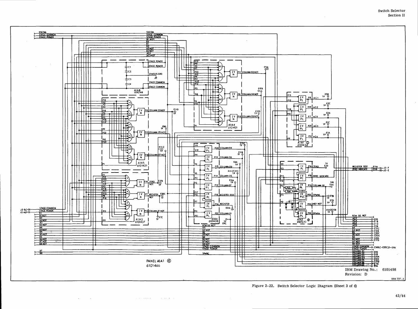
Switch SelectorSection II
SSCOM SSCOM
PANEL AIA16101466 o-tto
IBM Drawing No. :Revision: D
-E35CJ)-E9B
6101498
IBM T27-3
Figure 2-22. Switch Selector Logic Diagram (Sheet 3 of 6)
43/44
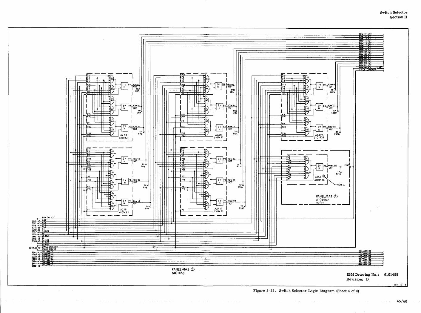
Switch SelectorSection II
• 610143 1
E2BA.B.C-O
PANEL A1A2
6101468 IBM Drawing No.Revision: D
6101498
IBM T27-4
Figure 2-22. Switch Selector Logic Diagram (Sheet 4 of 6)
45/46
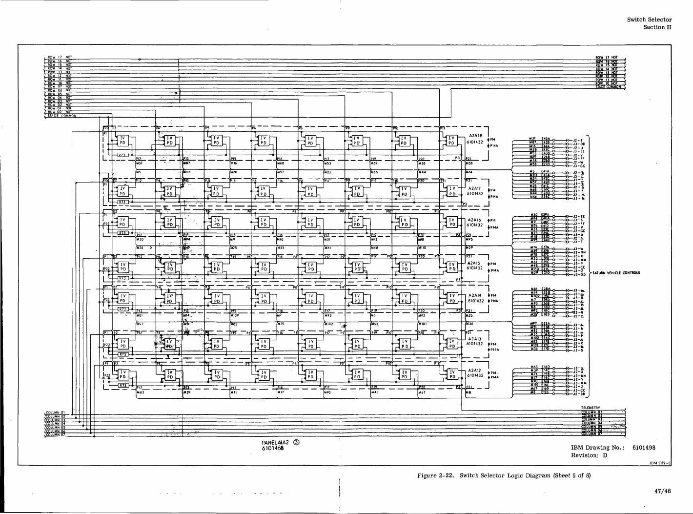
Switch SelectorSection II
PANEL /MA26101468
ROW 17 NOT
• SATURN VEHICLE CONTROLS
IBM Drawing No.Revision: D
6101498
IBM T27 -5
Figure 2-22. Switch Selector Logic Diagram (Sheet 5 of 6)
47/48
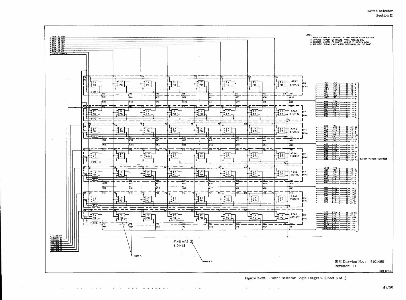
Switch SelectorSection n
ROW 17 NOTNOTES:
1. ABBREVIATIONS ARE DEFINED IN IBM SPECIFICATION 6101419.2. DENOTES NUMBER OF SHEETS PANEL APPEARS ON.3. DENOTES NUMBER OF BLOCKS MODULE IS BROKEN -INTO.4. ALL INPUT SIGNALS ARE WIRED INTERNALLY ON THE PANEL.
SATURN VEHICLE CONTSoU
IBM Drawing No.Revision: D
6101498
IBM T27-6
Figure 2-22. Switch Selector Logic Diagram (Sheet 6 of 6)
49/50
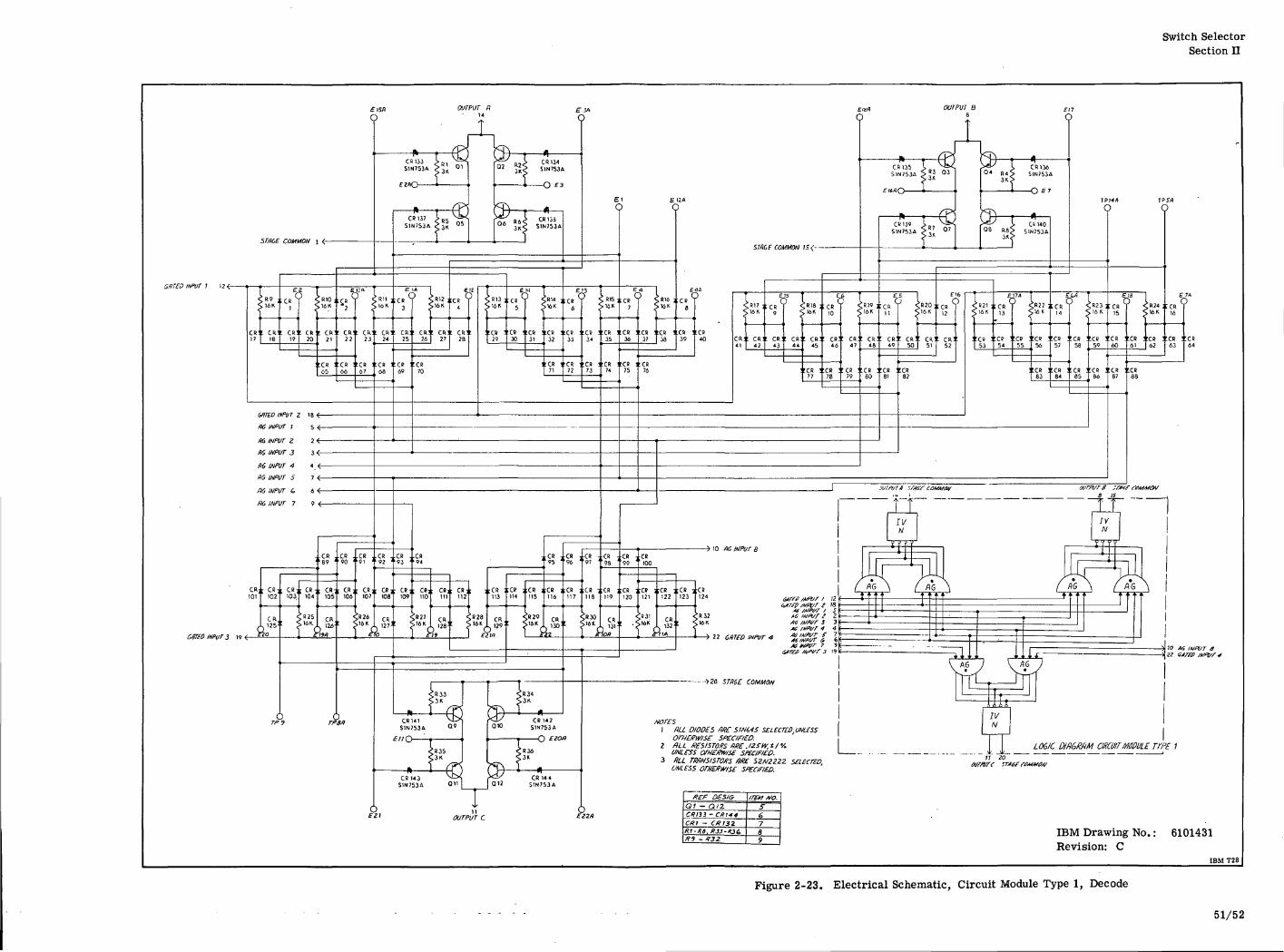
Switch SelectorSection II
sareo INPUT i
OUTPUT B
&fT£0 IHPUT3
5T//6E COMMON \ (STAGE COMMON !5<—
:LCR ::CR ::CR : :CR i:CR HCR VCR ! .CR ;:CR:: C R : t CR:: CR:: CR C»:: CR: : CR: : CR:C R : : C R : : CR: : C R : : C R : : CR:: CR: : C R : : C R : : C R : : CR: : CR ::ce ::c» : :CR ::CR ::c« : :CR ? : C R : :CR ::CR : :CR : :CR
:CR ; :CR ::c» : :CR ::CR : L C R : :CR : :CR : :cn : :CR : :CR
CR - .CR ..CR . .CR ,
C R ; ; ; ; C R ; ;CB ; :CB ; ;CR ; CR ;;CB iCR; : CR, : CR; C»] ; CR]
/MtVr I 12&trff /vfvr i IB
Al ff/PtV t S2
Mfvr s 34 4
AH Wft/r 7 93 19
> 22 CATfO INPUT t
->20 STH6E COMMON
' ' "~a_
1
li,
NOTESI flU. DIODES ffK£ S1N645 SEL£CrED,UHLESS
orHE/?tv/se SPECIF/ED.Z flU RESISTORS HKE. I2SW, t / %
10 AS fUPUT a22
I 1 I L06IC DIAGRAM CIRCUITMOLCIRCUIT MODULE TWE
3 HLL TMNSisroKs aKe SZNZZZZUNLESS
11 20STi
OUTPUT C
KEF OESIG-
CKI13 - CKI44Cflt - CK132
IBM Drawing No.: 6101431Revision: C
IBM T28
Figure 2-23. Electrical Schematic, Circuit Module Type 1, Decode
51/52
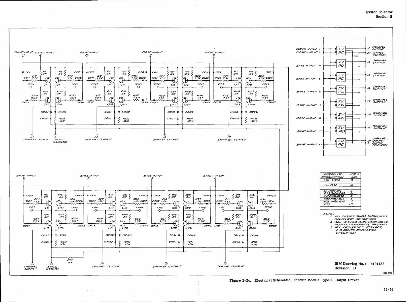
Switch SelectorSection II
cv-Q-ae/e/
XO
j UHi£SS
ffiM Drawing No.Revision: D
6101432
IBMT29
Figure 2-24. Electrical Schematic, Circuit Module Type 2, Output Driver
53/54
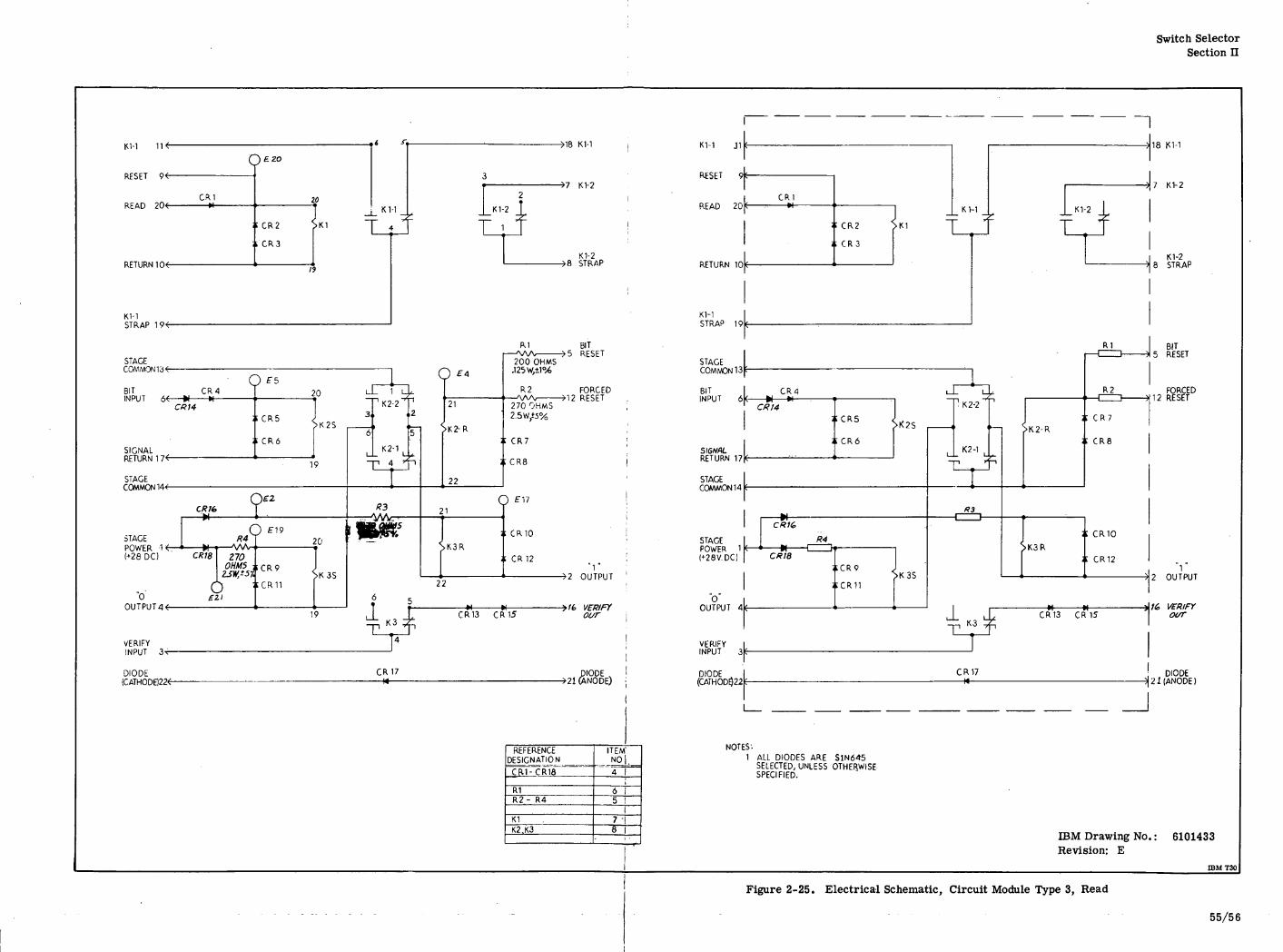
Switch SelectorSection n
cRESET 9<
CR1
KV1
STAGE
BIT CR4
CK141
1
SIGNAL
STAGE
• 4 <"• ^1ft K1 1 K1 1 11
3 RESET 9
T II | K1-1 \ I K1-
; CR2 SKI "T 4 T T* 1; CR3
-) E 5 y f4
20 J_ 1 d^1 ' K 2 - 2 ' 21
I C R 5 |K^ 3' "2 J
6 5 f-K2LR
19 ~r 4 n '22
O" ,_ Cc*'6 T . SA 21 ]
STAGE K4POWER 1 < — • M"1 — VW-<(+28 DC) CR18 no
OHMS ;
O '0 £2.1
VERIFY
DIODE
,. .... j..?"- ["
y ^19 | 0^Ri ;
K 3S i, CR 11 2^
? 5
5 (2 T READ 20
*T |
K1-2
K1-1STRAP 19
R1 BIT— V\A^ >5 RESET
200 OHMS STAGE.125W,±1% COMMON 13
R2 FORCED BIT
270 OHMS
E CR7SIGNAL
f C R 8 RETURN 17
STAGECOMMON 14
CR10STAGEPOWER 1
s CR 12 ! (+28V.DC)V
"o"19 .1 L CR13 CR15 0^r
T1 K3 T' 4
CR17
VERIFYINPUT 3
DIODE DIODE
REFERENCE ITEM' NuT£
DESIGNATION _ N0|.
1
R1 6R2- R4 5 !
IK1 . 7 -|K2.K3 8 i
i •
-
\
IC j
C R 1
1^ \ _LK M_L J_K1-2 L
1 T ti ; CR3
R1
\ ^^\
CR4 i_L l_^ R2
CR14 I ! K2'2 I-CR5 { J ; ; c R 7
' >K2-R
;; CR6 ;: CR8, ,.. ,, I U . ^^L^
^ T . T
PI •' " 1 \ f1
CR1t>
R4 J
c*'8 \ . \ i: CR12
SK 35 1 i >|KCR11 [
J_ J, CR13 CR15
L-
CR17M "J™ 1
1
7 KV2
K1-28 STRAP
BIT5 RESET
FORCED12 RESET
12 OUTPUT
16 VERIFYovr
DIODE21 (ANODE)
s-.1 ALL DIODES ARE S1N645
SELECTED, UNLESS OTHERWISESPECIFIED.
IBM Drawing No. : 6101433Revision: E
IBMT30
Figure 2-25. Electrical Schematic, Circuit Module Type 3, Read
' - - 55/56
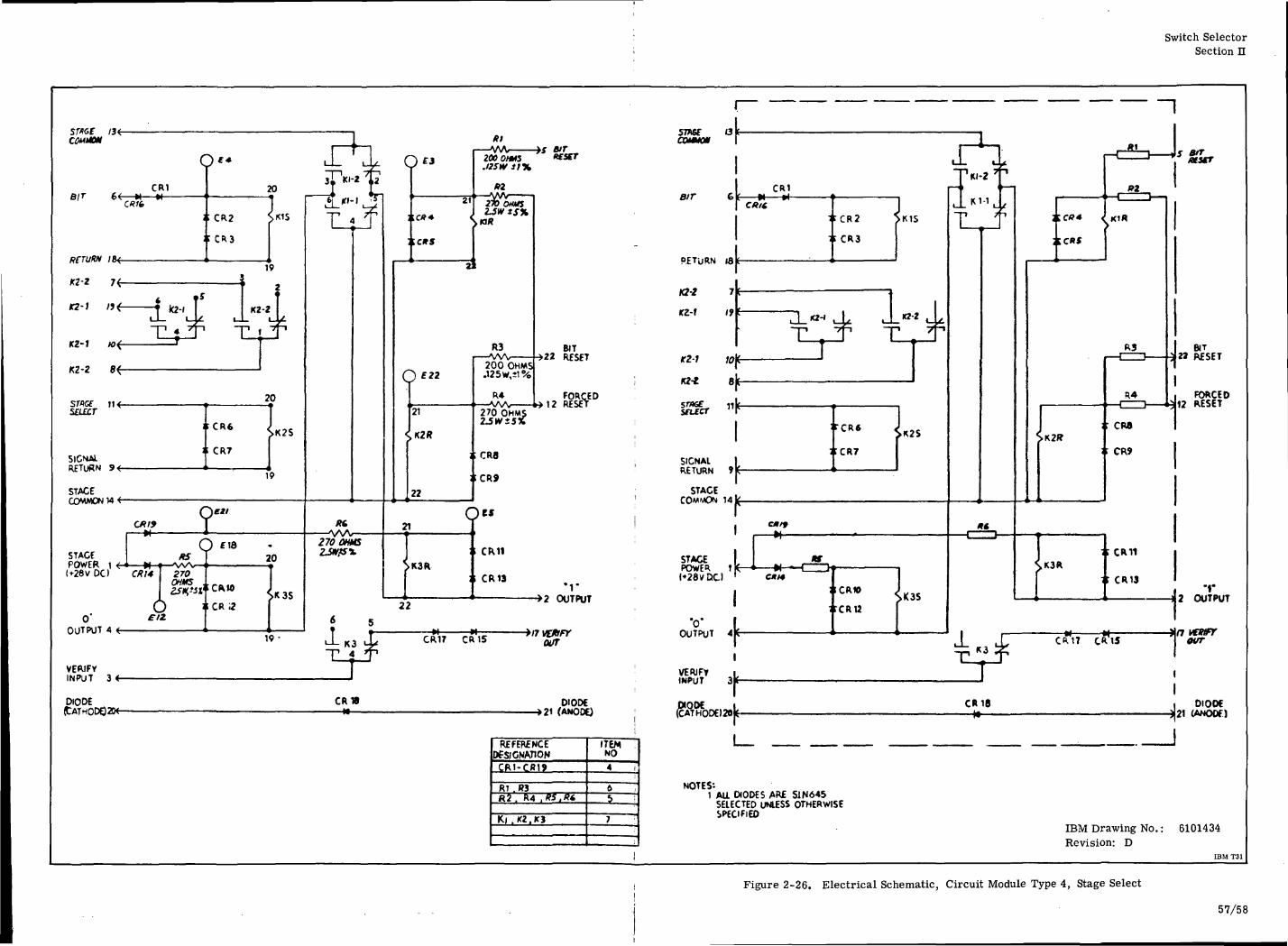
Switch SelectorSection n
KZ-1
K2-2
saxcr
SIGNALRETURN
STAGECOMMON 14 <-
STAGEPOWER 1 <-(+28V DC)
0OUTPUT 4
cCR1
i
i
/
( 4 t*
1 1 1 Ix
T j^T
/\
i
1
CKI9
CR14 I 270OHHS .asu^v
6 >eiz
?**20
CR2 S^S
' CR3
19
" 2
K2-2
111 7 '1 - 7 "I
20
ICR6 SK2S
t CR7
19
r") £18
20
;c*w Just C R ^ j
3u *'
H4
«270 OM2J*5tf1
»
r2'f
r^
«sk
5
r
c
<
21
J
[22
}"
21
;c»« <
;c»5
2!
?£"
21
K2K
\
»
22
C
4
1 VA2000H*5.125 W i/%
#2, _iwy^ .
27D OHUSriR3
1 W\200 OHMS
R4i Ww
270 OHMS2JIV±5X
:CR8
ICR9
?"CR11
; CRis
KfSCT
BIT>22 RESET
FORCED• 12 RESET
*r-»2 OUTPUT
19- CR17 CR15
VERIFYINPUT 3 «-
!» ^7^
T I TOUT
DIODE CRW—M
DIODE-»21 (ANODE)
REFERENCEDESIGNATION
CR1-CR19
Rl .nR2 . R4 , R5,R6
Kl .K2.KJ
ITEM ,NO4 ij
65 :
7
57MFCOMMOV
e/r 6
P.ETURN (8
irz-f 19
CR1£ M *-
KZ-1 WF~
4-
SIGNAL IRETURN »t
STAGECOMMON
STAGEPOWER
T
•o- IJTPUT 4K-OUTPUT
VERIFY iINPUT 3*
T
-W-(«28v DC) ' CUM
I
NOTES'-1 AIL DIODES ARE S1N645
SELECTED IMESS OTHERWISESPECIFIED
T
•w-
<M
1K3
CR18
'.K2R
~1
R3
; • CR8
: CR9
It CR13
JUT C?15C R U
RESET
, FORCEDJl2 RESET
T2 OUTPUT
T vesfrour
DIODE
IBM Drawing No.Revision: D
6101434
Figure 2-26. Electrical Schematic, Circuit Module Type 4, Stage Select
57/58
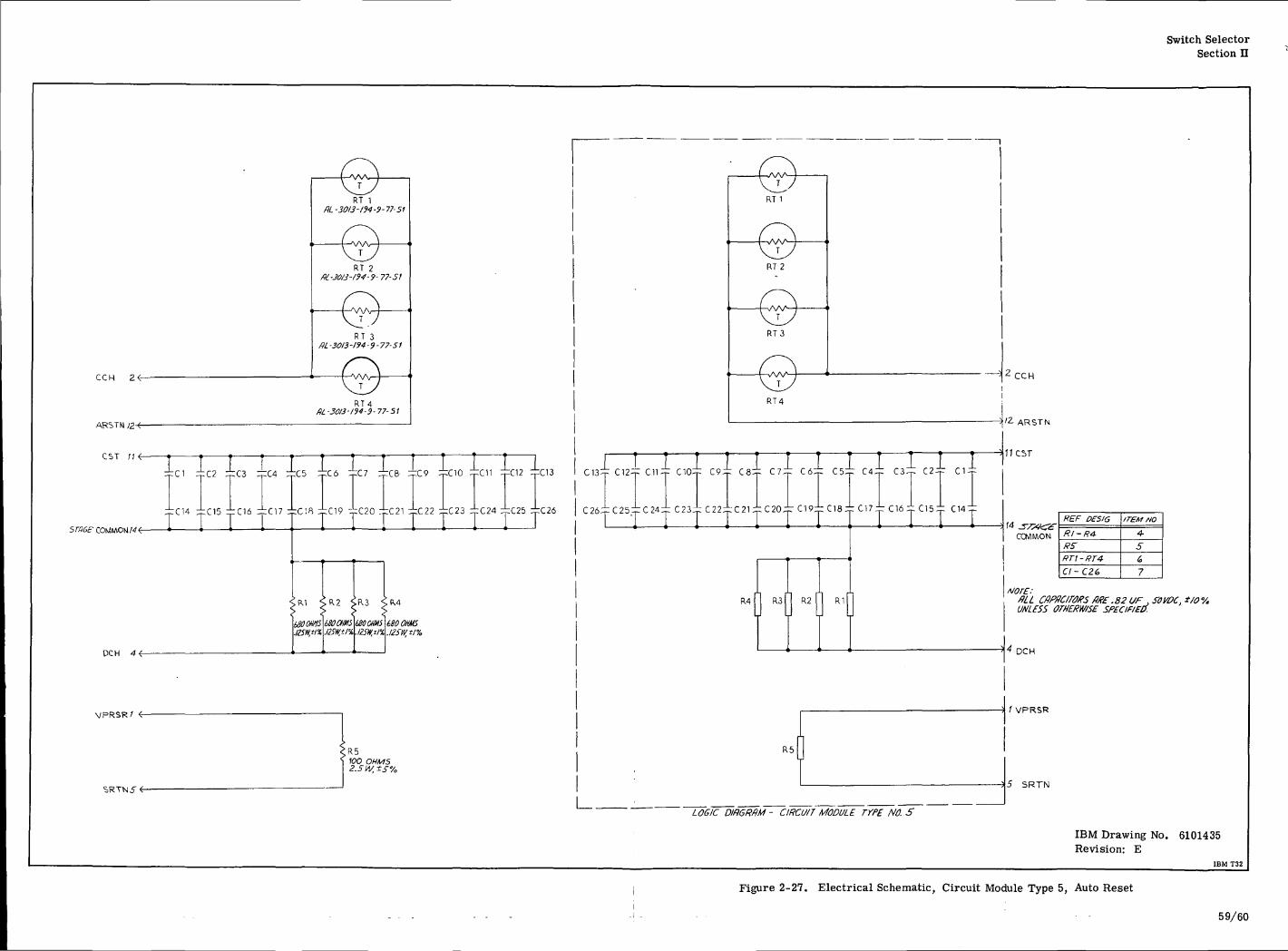
Switch SelectorSection n
CCH
ARSTN /2-e
CST 77 <r-
ici ±C2 ;b
R.2 SR3
,=r„=,
:f CU^f CKPF C9^ C8i C7
iC25i:C24^ C23
R4
DCH
VPRSR/
,/2SW,i/%MOOHMS 680 OHMS
.!2SlVtl%
R3 0 M0 "0
R510O OHMS2.5 W, ±5%
R5
LOGIC DIRGRftM - CIRCUIT MODULE TYPE NO. S
-: 2 CCH
'2. ARSTN
11C5T
| COMMON RI-R4ffS~
RT\-RT4
C/-C26
ITEM fJO
S
A/Or£:ffLL CflPflCirOKS flfff .82 UF . SOWC. */0%UNLESS OTHERWISE Sf>£CIFIE[t.
DCH
/VPRSR
S SRTN
IBM Drawing No. 6101435Revision: E
IBM T32
Figure 2-27. Electrical Schematic, Circuit Module Type 5, Auto Reset
59/60
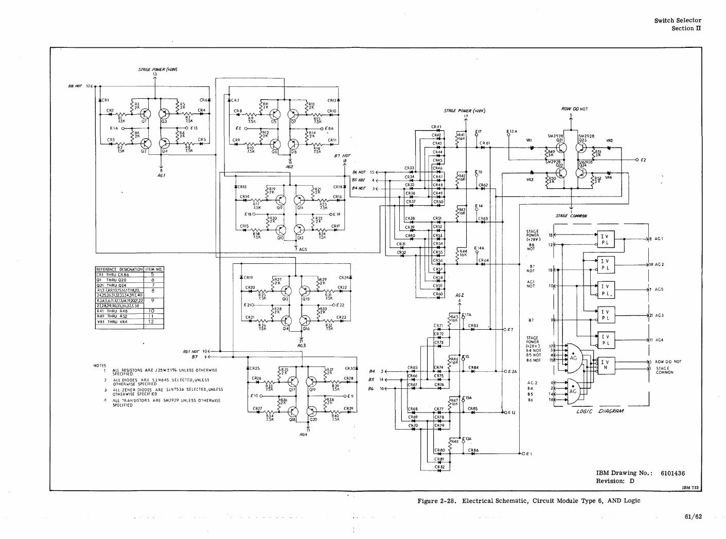
Switch SelectorSection n
57R6E POWER (tZiV)13
ROW 00 NOT
REFERENCE DESIGNATION
CR1 THRU CR8601 THRU Q20
021 THRU 024R1,2,7,8,9,10,1S,16.17,18.23,24,25,26JU23a3439.£.40
R 3.4,5.6,11.12.1 3,14,19.2021,2227,28,29,30,3S,36,37,t38
R41 THRU R48R49 THRU R52
VR1 THRU VR4
ITEM NO.
5678
9
101112
NOTES1
f/6t norB7
ALL RESISTORS AKE .125W±1% UNLESS OTHERWISESPECIFIED.
ALL DIODES ARE S1N645 SEL ECTED, UNLESSOTHERWISE SPECIFIED
ALL ZENER DIODES ARE S1N753A S E L E C T E D , UNLESSOTHERWISE SPECIFIED
ALL TRANSISTORS ARE SM2929 UNLESS OTHERWISESPECIFIED
O £2
5 ROW 00 NOT
IBM Drawing No.:Revision: D
6101436
IBM T33
Figure 2-28. Electrical Schematic, Circuit Module Type 6, AND Logic
61/62
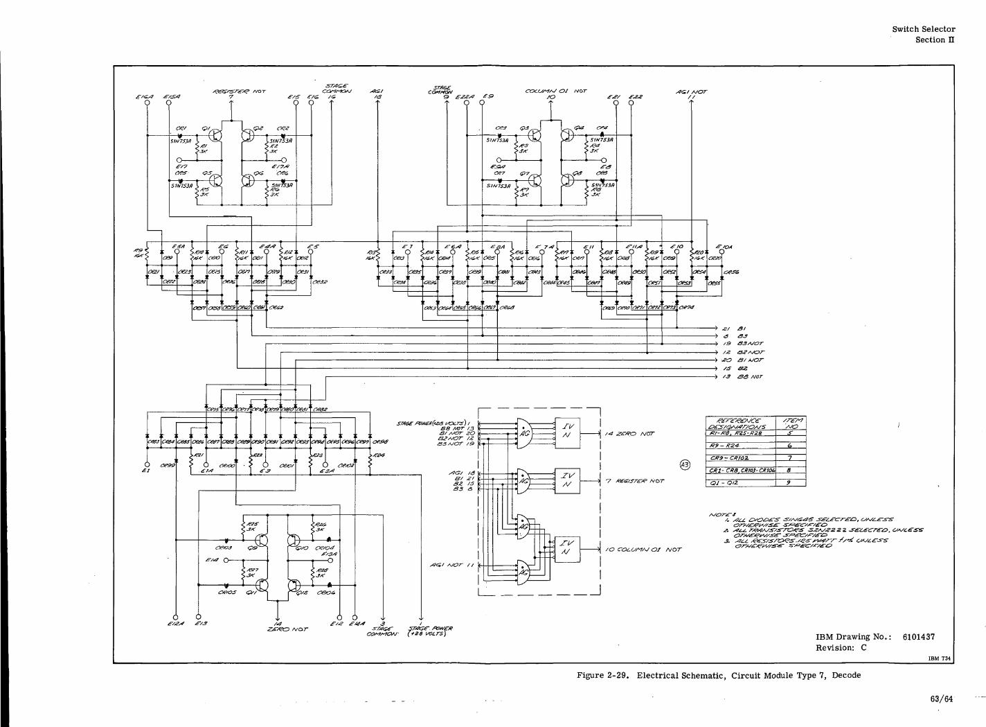
Switch SelectorSection n
(+28 VOLTS) IBM Drawing No.Revision: C
6101437
IBM T34
Figure 2-29. Electrical Schematic, Circuit Module Type 1, Decode
63/64
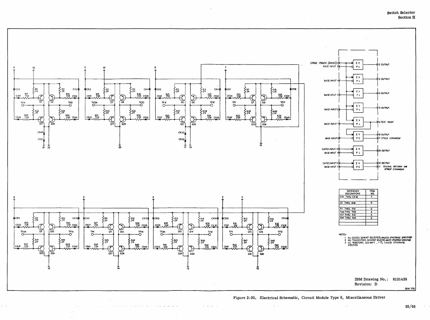
Switch SelectorSection H
ICR15 S R1S>2K
12
(Z8YDC)3BASE INPUT 2
BASE INPUT 4
BASE INPUT 5
BASE INPUT 6
E1ASE INPUT 7
BASE INPUTS
CATED INPUT 19
BASE WPUT 9
GATEDINPUT10
BASE INPUT 11
;
£
k —
£ —
e —
— c
— c
— c
— Ci
c
— c
I V
P L
I V
P I
I V
P L
I V
P L
I V
P L
I V
P C
I V
P I
P C
,
12 OUTPUT
13 OUTPUT
14 OUTPUT
15 OUTPUT
*16TEST POINT
•J 18 OUTPUT
17 STAGE COMMON
20 OUTPUT
-3)22 OUTPUT
SIGNHL RETURN OHsrase COMMON
REFERENCEDESIGNATIONS
CR1 THRU CRS2
01 THRU 032
Rl THRU R16R33THRU R4SR17 THRU R32R49 THRU R64
ITEMNO.7
8
66S5
NOTES'1 All DIODES S1H61S S£LCCTeD,UNieSS HTHE/tHISf SffCIFICD2 ALL TRANSISTORS S2/V2907 5£L£cra> IM.KS aTHffWaCSfK/FICD3 AU RESISTORS .125 WATT . ±1% UNLESS OTHERWISE
SPECIFIED
IBM Drawing No.:Revision: D
6101438
IBMT35
Figure 2-30. Electrical Schematic, Circuit Module Type 8, Miscellaneous Driver
65/66
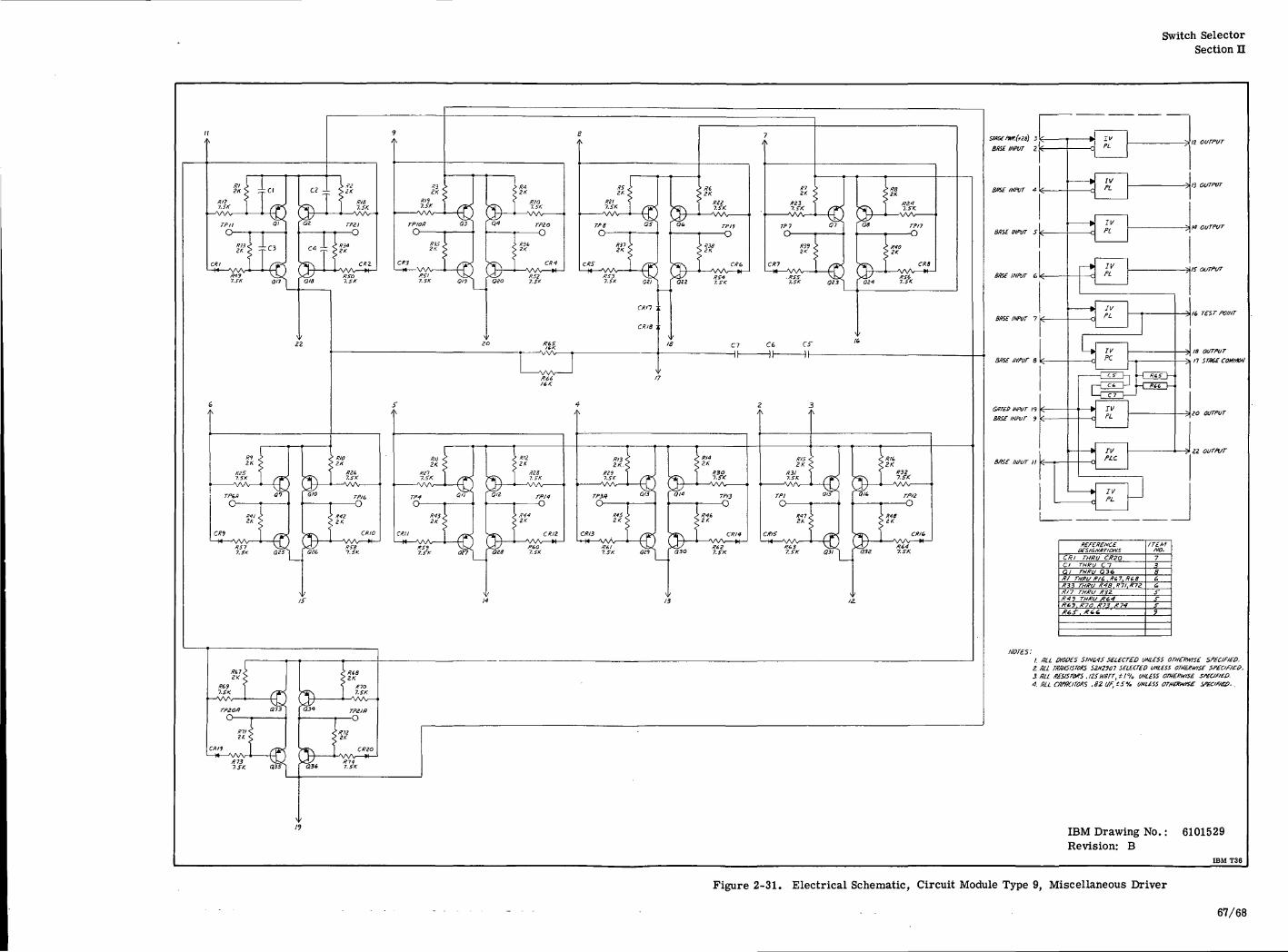
Switch SelectorSection n
^ a OUTPUT
It TEST /VINT
IS OUTPUT11 5TO6E COMHXN
REFERENCEXSIGNflTIOHS
CKI THRU CK2OCl THRU C7Qf THRU Q36#/ rvfl//f/6,M7.K6SK33 THKU K48.RTI.mZKH THKU #32.K-tl THKU fte.4Rt?,K70.K73.f7->#&f. ft,&
ITEMNO.738£&s-s-f9
NOTES:/. /ILL DIODES SINUS SELECTED UNitSS OTH£KW/S£ SPECIFIED.2 BU. tf/IMSISmte S2/t2)cn SELECTED UKLESi ew&nwsf SP£Of/£!>.3./ILL Kfsis rats. izf tvarr, */% UNLESS ome/nv/se specjf/eo.4 HLL CAPtiCimte .S2UF,±5% Vf/LfSS OTH£KtVK£ Sf£Clf/Ep. .
IBM Drawing No.: 6101529Revision: B
IBMT36
Figure 2-31. Electrical Schematic, Circuit Module Type 9, Miscellaneous Driver
67/68
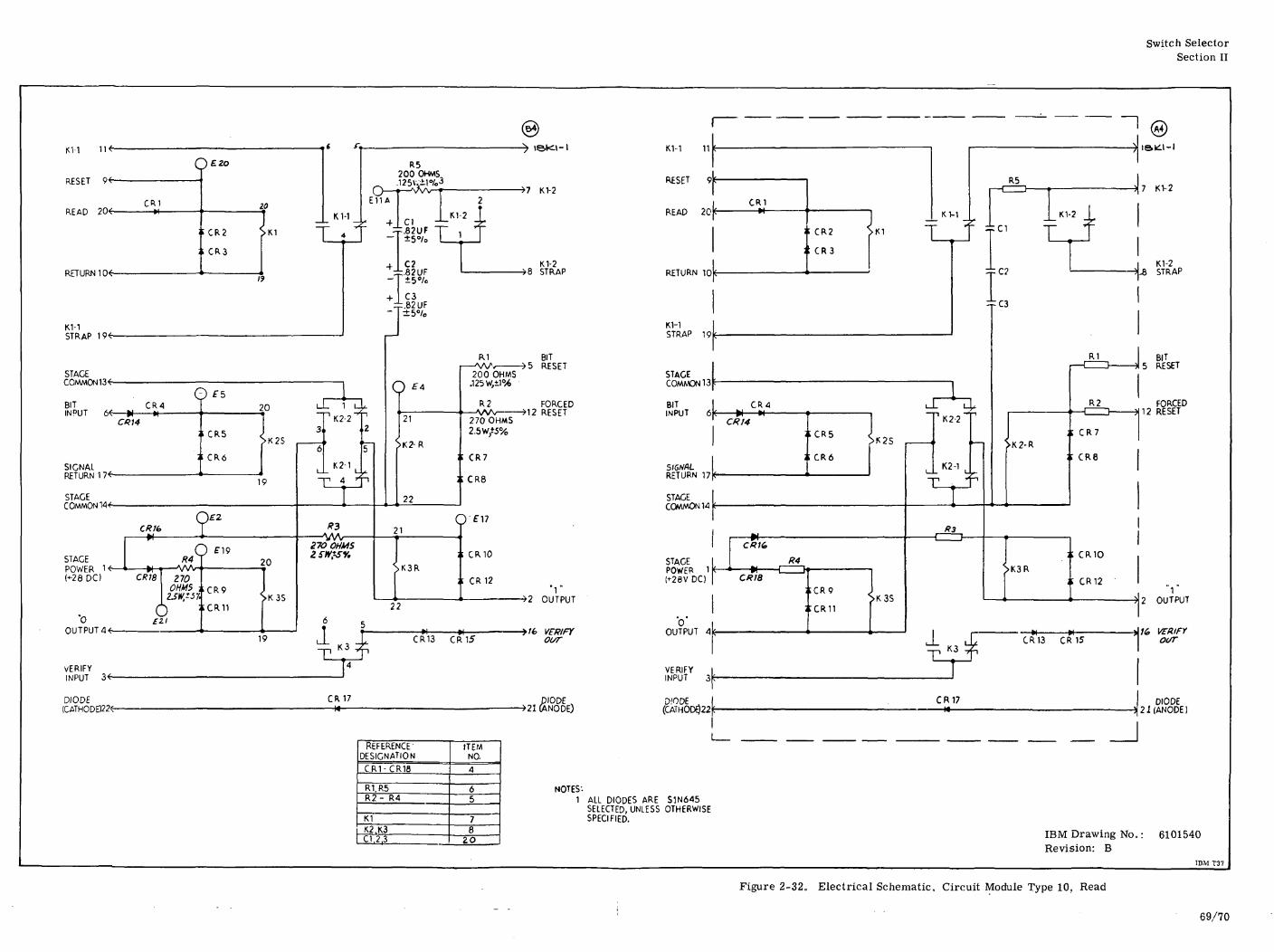
Switch SelectorSection II
K1-1 IK-
RESET 94-
O£2°
READ 20*-CR1
W-
RETURN10*-
KMSTRAP 19«
STAGECOMMON 13 <-
- C R 2
R5200 OHMS
o —E11A
^ .X KI-2
2
1K1
: CR3
?
T * T 4;F-821JF TI i I - iS'/o L
BITINPUT 6<-
C R 4O
CR14
SIGNALRETURN 1 7<~
J T l Z L
3,
CR6
STAGECOMMON 14*-
C/?/6
STAGEPOWER 1<-(+•28 DC)
•oOUTPUT4<-
O E T
-w-i—^AVCRIB no
^?,icR9
(!) '"" K 3 S
,2
5"
K2-1 .
4 Tn
^WV-2^? OHMSi fHffS%
KV2
ri.82UF
±5°/o
K1-2STRAP
.±5°/o
P.1
21
22
200 OHA/S,125W,±1%
R2-AAAv270 OHMS2.5W/S%
; ; C R 7
; ; C R 8
BIT>5 RESET
FORCED>12 RESET
21O
K3R
22
;; CR10
;; CR12T
OUTPUT
19
U
1K3
VERIFYINPUT 3<r-
CR13 CR15 our
DIODE(CATHOD022e
CR17M
DIODE ,->21 (ANODE)
REFERENCEDESIGNATION
C R 1 - CR18
R1.R5R2- R4
K1K2.K3C1,2,3
ITEMNO.
4
65
78
ZO
K1-1 11
RESET 9
READ 20
RETURN
K1-1STRAP 19
STAGECOMMON 13
BITINPUT 6
SIGVfli.RETURN 17
STAGECOMMON 14
STAGEPOWER 1(+28V DC)
0OUTPUT 4
VERIFYINPUT
DIODE . .(CATHODE)22t
NOTES'.1 ALL DIODES ARE S1N645
SELECTED, UNLESS OTHERWISESPECIFIED.
CR1M-
; ; CR2; ; C R 3
-W-CR4
ii CR6
R4
CK18
;;CRII
KM
R5
i:C2
:fC3
>K2S
>K3S
K2-1
T ?
R3
K1-2
T
R1
R2
; ; C R 7
; ; C R 8
>K3R
1K3
-Vr-CR13 CR15
CR17
7 KV2
KI-2STRAP
BIT5 RESET
FORCED12 RESET
;; CR10
\ \ CR12 '1
2 OUTPUT
76 VERIFYot/r
DIODE21 (ANODE)
IBM Drawing No.: 6101540Revision: B
IBM T37
Figure 2-32. Electrical Schematic. Circuit Module Type 10, Read
69/70
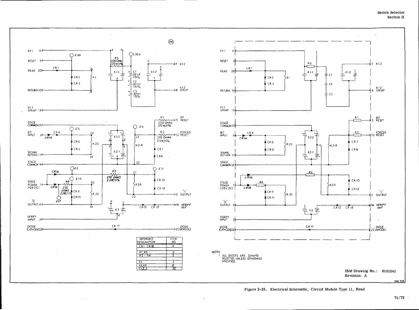
Switch SelectorSection n
K1-1 11 <-
QH20
RESET 9«-
READ 20<-CR1
—w-
RETURN 1CK-
K1-1STRAP 19<
STAGECOMMON13*
BITINPUT 6<r
SIGNALRETURN 1 7<
STAGECOMMON 14
STAGEPOWER 1 *(+28 DC)
"0'OUTPUT44
VERIFYINPUT 3<-
; CR3
( /9
Kl-2
Kl-2STRAP
R1
C R 4f U u
CR14t
P f 520 u
: CR5 <
i CR6
> K 2 S
19
0«<** I
.// • i M • A.AA.I
c>?;« £70(3//WS ;zsiv, -' r.
6£27
") £1920
: C R 9
;CRHK 3S
3,
6
L
ZTiZS
1
n K2
L_
• K M L
p 4 *
R3WV•)OHi,tffS
5f
2
5
.
~\
1 5K
5
(
<
?^
21
>K2-R.
22
c21
SK3R
I
200 OHMS.125W,il%
R2
270 OHMS2.5W;5%
; CR?
: CR8
? £1?
; CR10
S CR 12
22
*i >i *
BIT5 RESET
FORCED12 RESET
19
TL"CR13 CR15
' .1OUTPUT
VERIFYour
DIODE(CATHODE)22e
CR 17—M >21
DIODE(ANODE)
REFERENCEDESIGNATION
CR1- CR18
R1.R5R2 - R4
K1K2.K3C1.2.3
ITEMNO.
4
65
7820
K1-1
RESET 9K
READ 20
RETURN 10
KMSTRAP 19
CR1M-
CR2
C R 3
STAGECOMMON 13p
BITINPUT 6
SIGNALRETURN 17
STAGECOMMON 14
STAGEPOWER 1I+28V DC)
OUTPUT 4k-
VERIFYINPUT 3
DIODE(CATHOD022
NOTES'.1 ALL DIODES ARE S1N645
SELECTED, UNLESS OTHERWISESPECIFIED.
K1
R1
K3CR13 CR 15
CR1714
7 K1-2
K1-28 STRAP
F
,
C R 4-W W '-RI4
i
i
CK1(,
R4
CKI8
S C R 5 SK2S
i CR6
; C R 9 JSK 35
;cRii [
J
i_1
' K2
K2
r
/?.^
.J
-1
1
9ZJ—
U-i
• -
r
<
]i
I -.>K2-R
[
. i
M 1
1 1 f
L R2
( CR7
: CR8
; CRiO
: CR12
BIT5 RESET
FORCED*\2 RESET
12 OUTPUT
/6 VERIFYour
DIODE21 (ANODE)
IBM Drawing No.Revision: A
6101541
IBM T38
Figure 2-33. Electrical Schematic, Circuit Module Type 11, Read
71/72
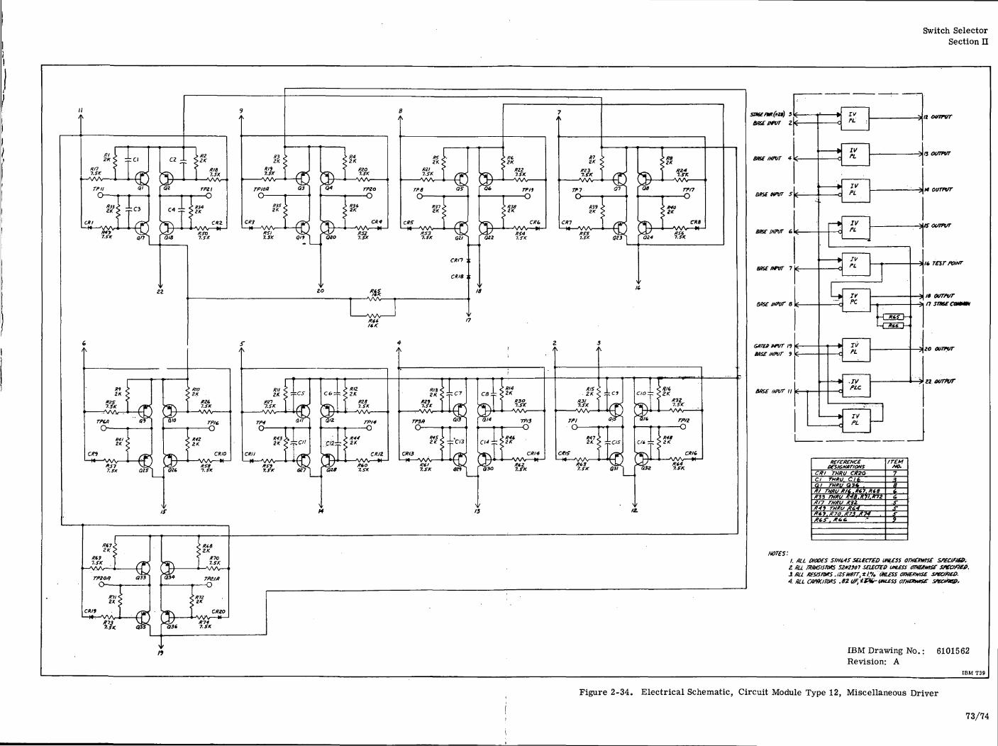
Switch SelectorSection n
snecnmfra) toast INPUT z
BKf HOVT 4
B*Sf MPUT S (.
BOSf INPUT
e/Kffffor 7
ftdSf INPUT 8
use INPUT 9 i£
a/Kf IHH/T n
£
^^
s~**
^ .*•
^^t
J*s-
x
*•
£sv
^
L
a ft
i ft
\ ft
i ft
ft
— • ft
.
ry«.
IVPL
IVPL
IVPL
IVPL
IVPC
IVPL
PLC
•;•
PL
\
te
— ?
>- *
•— ~3
^
|
. .x
REFERENCEIfSKHfTIOHS
CRI THRU CR2OCl THRU, CI6_Ql THRU O3* ,/?/ THRU K/t Xtl.RtS#33 THKV f4B.K7l.fm#17 rHXU K31#41 THKU #64f*f?,#70.#73.f?4 .K6S". #64 •
ITEMMO.738
&fs-
*
OUTPUT
13 OUTPUT
OUTPUT
a OUTPUT
It TEST POINT
IS OUTPUTn snsecammt
IO OUTTVT
OUTPUT
NOTES:/. ALL O/OOfS SM64S SELCCTCD UWfSS OTHBWSf SP£ClflO>.t /ILL mueisToK szn2)<n safofo UNLESS cmexivisf speaft£t>.sou xfsan*s./zfMTT,ti% OHLfssomE/wtsf steateo.4. HLL OWKlTOKS .82 UF,tT>ik-VHLtSS 0m£XM»S£
IBM Drawing No.: 6101562Revision: A
Figure 2-34. Electrical Schematic, Circuit Module Type 12, Miscellaneous Driver
73/74
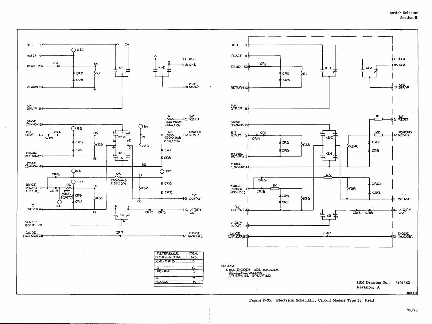
Switch SelectorSection n
K l - l 7<-
ORESET 9<
CRIREAD eCK *-
;;CRZ
zp
1- O
&> i>»
13
Kl-lSTRAP fi><-
IT tf
-» 11 M-Z.
-» 16 Kl-Z.
5TAGECOMMON 184
BIT
SlGMAURETURN 17 4
STAGE
POWER I*
"O'OUTPUT 44
VERIFVINPUT ^DIODE: CRI7
M—
<\-Z->I2> STRAP
Rl
Iff
c
)
4< —
CR^
JR14-
CR1Q,
CRIB
E2
C
t
t
\c
Z7OOHMS ;
; =:i
") E5
i<
P^
") El^
;cw;CRi\
P
1
5
O
K35
iJ
3
u~
A
Z~K
1
rJ-> .-2
K2
r 4
50UJ
&r
^_ ~ ?
i_i. »•
>J15> /O
I*
5
/r
5
C
<
8
J
Zi
")E4
ai
>K2-R4
J
3Z
C1
i
i
9
EOOOUM5.I25\^i 1 j4
37OOUKAS
i CRT
;CR&
; CRIO
; CRe
BITRESET
FCRCEDRESET
fe
OUTPUT
->l& \)ERlP^our
DIODE-»3I CAMOOE)
RCFERENX.E.
CRI-CRie>
P.IR^-Rd-
K.IK.Z.W12.
ITEMMO.4.
fe&
7&
Kl-l 7 f
RESET
READ ZO
RETURN 10
Kl-lSTRAP S
STAGE ICOMMON laf-
BiT110PUT
RtTURM »7
5TASE.COKAMOW14
STAfeEPOXWER 1
(+ZSVDC)
OUTPUT 4rUERlFVUEWIFY lIMPUT 3f
OlOOE.
CRlW-
3: ORE.
j;CR3
< m *CR14
2
L
MCRltb
R4
*CRII
I. &LL. DIODES ARESELECTED, UtOLE-SSSPECIFIED.
LT
^
1 ; CR6
::CRI°>K3R
1-w w-
CR\3 CRlb
CR17
^ I1?! STRAP
FORCE.Oe RESET
»,.
|E OUTPUT
^l& VJERlFVOUT
DODE(AMOOE.')
IBM Drawing No.Revision: A
6101563
IBMT40
Figure 2-35. Electrical Schematic, Circuit Module Type 13, Read
75/76
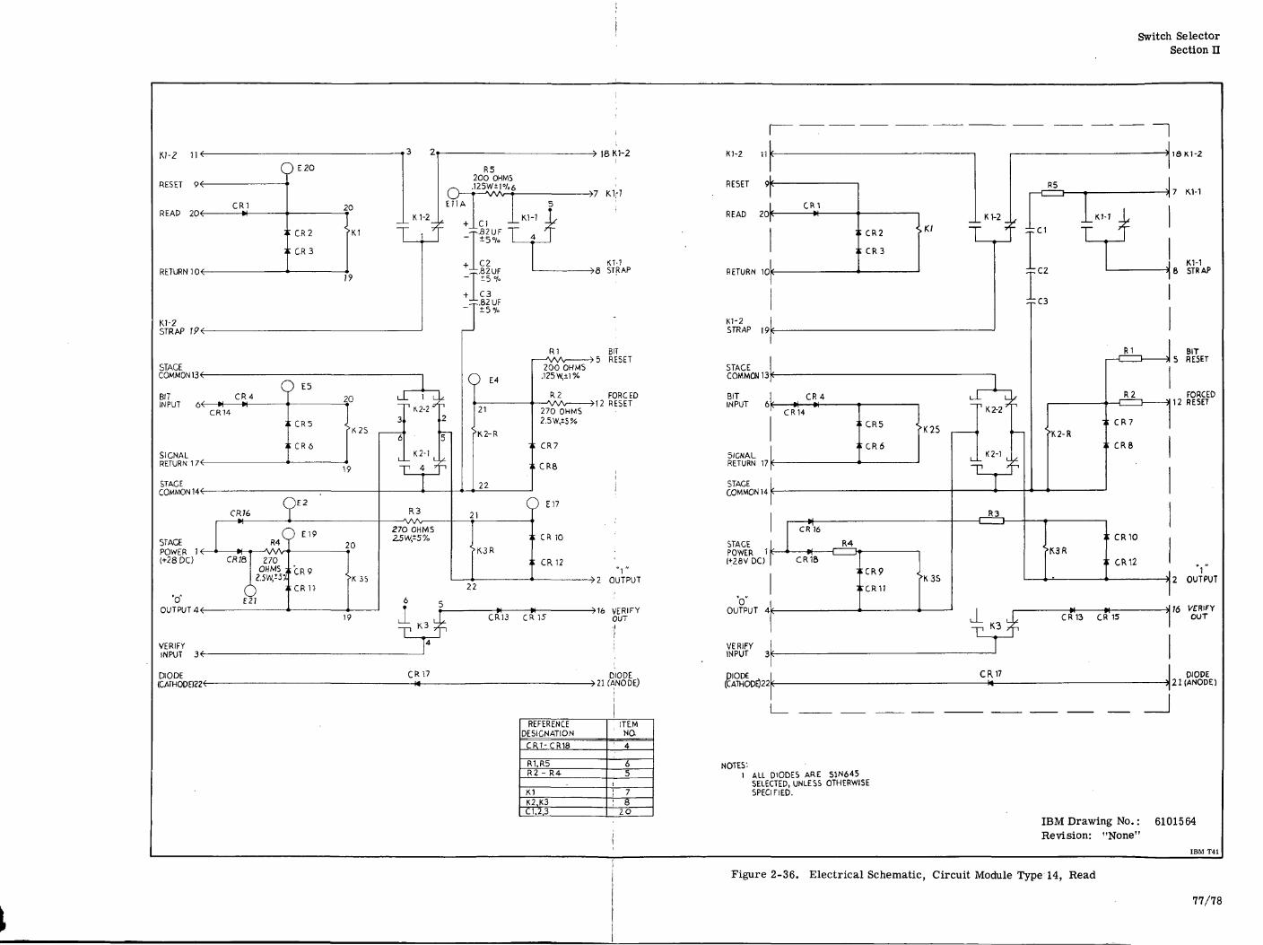
Switch SelectorSection n
OE2° R5ci~TT o< T 200 OHMS
C R J 2 0 EI1A I f iI f\ 1 -£. 1 f\ | - J | x *•
: ; C R 2 JK1 T 1 T -T + |VF "Q_4_J
; ; C R 3+ C2 KM
19 - ±5%
+ C3i.82UF
~ ±5%
K1-2 " K'-2
R1 BITi WV >5 RESET
STAGE 200 OHMS STAGE
BIT CR4 20 L-L 1 L_L R2 FORCED BIT
CR14 K2'2 21 270 OHMS; ; C R 5 1 3 '2 J 2.5W,±5%
6 5 K2 R
-; CR 6 ~<; CR7SIGNAL x L K2-1 L^ S/CNALRETURN 17< * ^ 4 Ji., H C R 8 RETURN 17
STAGE __ 22 STAGE
O" oo O E'7CR»,76 T -*? 21 Tr~> r,n 27O OHMS( ) E19 5ru/+Tiy - - r ft inSTAGE R4T 20 ^5W,-5 /c 1 - , L K 1 O ^^
(+28 DC) CR18 270 J I C R 1 2 ' (+26V DC)OHMS_K-CR9 J *1" '
Q a r C R I I - 22"0" f2I 6 5
! *o"
19 J_ iL CR13 CR15 OUT
VERIFY 4 VERIFY
DIODE CR17 DIODE , DIODE
REFERENCE ITEMDESIGNATION ' NO
CR7-CR18 4
R1.R5 6 NOTES'.R 2 - R 4 . 5 , A L L
i SELEK1 7 SPECK2,K3 8C1.2.3 2O
n
C R Tr * ' i J_ K 1-2 L
; : CR3
CR4 i_L i_Lk »t w " i ,, _ _ ' ' >
CR14 K2-2
L K 2 - , _
~P '1~l
R3
CR16
L R4
CR18
'
R5
J_K1-7 L
r T ^
:C3
R2•. 1 1 51•
1 •;; CR7
;; CR8
;; CRioI
;; CR12, ^
KCR11
t 1 1 I/
ICR17
CR13 CR 15
.
_J
18K1-2
7 M-1
K1-18 STRAP
BIT5 RESET
FORCED12 RESET
2 OUTPUT
16 VCRIFYOUT
I DIODE21 (ANODE)
DIODES ARE S1N645CTED, UNLESS OTHERWISEFIED.
IBM Drawing No. : 6101564Revision: "None"
IBM T41
Figure 2-36. Electrical Schematic, Circuit Module Type 14, Read
77/78
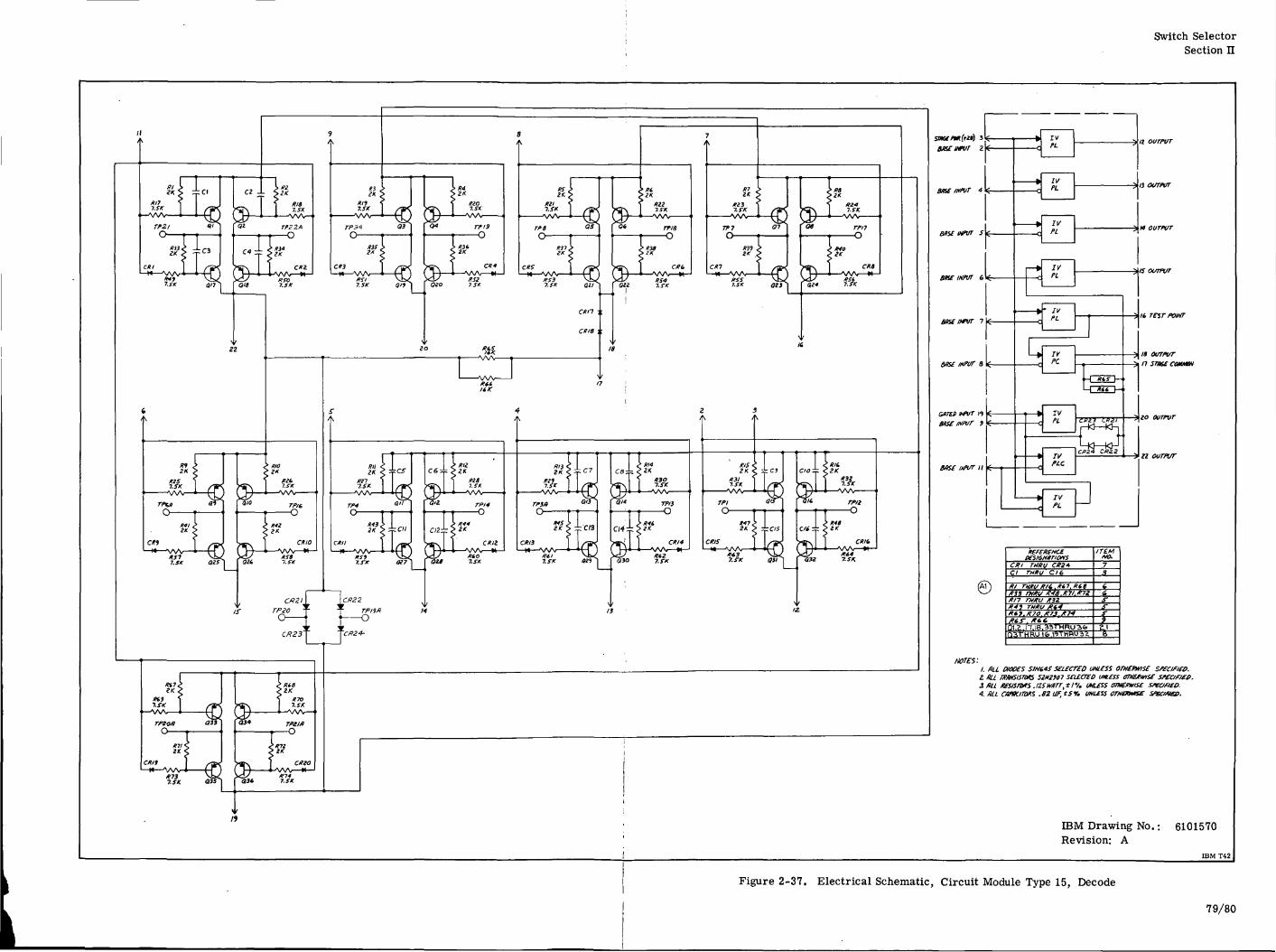
Switch SelectorSection n
1} OUTPUT
It TEST fOINT
OUTFVTII Srxf COMMON
OUTPUT
i. ffu otaofs sMeis seucreo UNICSS omenmsft RU nmns/sroG siw/n seacrtD UHLCSS tmcjtwsf sreaaee.3, an xesarvrs.asMirr,*!'/. VHL&S ometwae st-caneD.1. OIL OlffKlTORS .62 OF, tSV. UHUiS OTHOMKE SfKlflCP.
Drawing No.; 6101570Revision: A
IBM T42
Figure 2-37. Electrical Schematic, Circuit Module Type 15, Decode
79/80
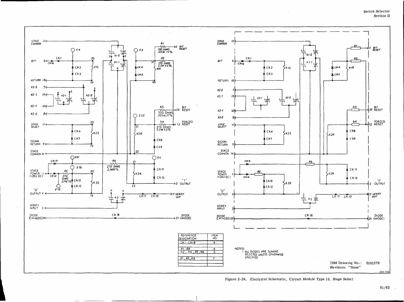
Switch SelectorSection II
STAGE /3eCOMMON
RETURN I8<-
K2-Z
K2-1 / ?<
K2-1 10 <
K2-2
saecr
SIGNALRETURN 9<-
STAGECOMMON 14 <-
STAGEPOWER 1 <-
OUTPUT 4 <-
Kl
9«CR1
:/?/6i
'.
: CR2
:CR3
3
« Ts
T K2-'ul_ i y i_
l_
20
^SK1S
f19
2
TK2-2 1
L i_U
T i^T T . ~ i
20
;
J s
CR7
19
Uv/y
CK14
Q«/
J
C/?5
270OHMS .C-J iff ••
oEIZ
") £18
CCRIOiCR12
20
]SK 3S
(
1
6
1
_ l_
, K'-2 ,
Kl-l ,_
4
^ 9"i2
7^f
—\
KG
27i? OHMS
21
i — vwZOO OHMS.I2SW U%
K2
270 OHMS.Cff4 J 2.5W*S%
\aR
ICRS
22
R3
C) £22
21
•^K2R
t
]
22
200 OHMS
R4AlAAj
270 OHMS2.5 IV ±5%
; CRS
C C R 9
0"21
<
]
E CR11
I CR13
22
6 5f » *J " ^ •
BIT>22 RESET
FORCED• 12 RESET
T2 OUTPUT
19"-L- K3T 4
VERIFYINPUT 3 <r-
CR17 CR15 OUT
DIODE(CATHODE)204-
CR 18M
DIODE21 (ANODE)
COMMON 4
BIT 6
RETURN (8
K2-Z 7
KZ-1 19
K2-1 W
K2-Z
STAGE
SIGNALRETURN ?|f
STAGECOMMON 14
STAGEPOWER 1(+28V DC)
OUTPUT 4
VERIFY iINPUT 3k-
DIODE i(CATHODE) 20 L
REFERENCEDESIGNATION
C R 1 - C R 1 9
R1 ,(?3R2 , R4 , RS ,R6
K1 ,K2,K3
ITEMNO
4
65
7
CR18
NOTES'-1 ALL DIODES ARE S1N645
SELECTED UNLESS OTHERWISESPECIFIED
C R 1 7 CR IS
**
CK/6
fe
IF
Lr
C
CR1
J_K2
'TL,
a/9H
RS5 — • m • i
CK/4
[
~4
I C R 2 ^ K 1
: CR3
IT ~L
.
; •c"' r' CK7
1
I>
1
4
;CRto JSK3
C C R 1 2 [
S
'^
S
s
1
u
L-
1
i
il
2 7-i
7 T
1 1
*6
j
t
<
LCR5
>K2RJ
.K3R
4
\ 1 '
R3
R4 ' j
: CRB
; CR9
r CRU
; CR13
^
— fcl u 'A
s BIT
BIT22 RESET
FORCEDRESET
"1"2 OUTPUT
VERIFYOUT
DIODE(ANODE)
IBM Drawing No.: 6101578Revision: "None"
Figure 2-38. Electrical Schematic, Circuit Module Type 16. Stage Select
81/82
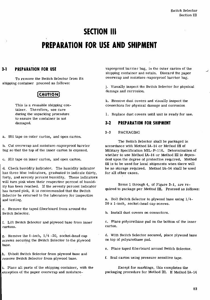
Switch SelectorSection in
SECTION III
PREPARATION FOR USE AND SHIPMENT
3-1 PREPARATION FOR USE
To remove the Switch Selector from itsshipping container proceed as follows:
£CAUfjpNJ
This is a reusable shipping con-tainer. Therefore, use careduring the unpacking procedureto ensure the container is notdamaged.
a. Slit tape on outer carton, and open carton.
b. Cut overwrap and moisture-vaporproof barrierbag so that the top of the inner carton is exposed.
c. Slit tape on inner carton, and open carton.
d. Check humidity indicator. The humidity indicatorhas three blue indicators, graduated to indicate thirty,forty, and seventy percent humidity. These indicatorswill turn pink when their respective percent of humid-ity has been reached. If the seventy percent indicatorhas turned pink, it is recommended that the SwitchSelector be returned to the laboratory for inspectionand testing.
e. Remove the taped fiberboard from around theSwitch Selector.
f. Lift Switch Selector and plywood base from innercartons.
g. Remove the 1-inch, 1/4-20, socket-head capscrews securing the Switch Selector to the plywoodbase.
h. Unbolt Switch Selector from plywood base andremove Switch Selector from plywood base.
i. Place all parts of the shipping container, with theexception of the paper overwrap and moisture-
vaporproof barrier bag, in the outer carton of theshipping container and retain. Discard the paperoverwrap and moisture-vaporproof barrier bag.
j. Visually inspect the Switch Selector for physicaldamage and corrosion.
k. Remove dust covers and visually inspect theconnectors for physical damage and corrosion
1. Replace dust covers until unit is ready for use.
3-2 PREPARATION FOR SHIPMENT
3-3 PACKAGING
The Switch Selector shall be packaged inaccordance with Method LA-14 or Method in ofMilitary Specification MIL-P-116. Determination ofwhether to use Method LA-14 or Method III is depen-dent upon the degree of protection required. Methodin is to be used for local shipments when there willbe no storage required. Method LA-14 shall be usedfor all other cases.
Items 1 through 4, of Figure 3-1, are re-quired to package per Method in. Proceed as follows:
.a. Bolt Switch Selector to plywood base using 1/4-20 x 1-inch, socket-head cap screws.
b. Install dust covers on connectors.
c. Place polyurethane pad on the bottom of the innercarton.
d. With Switch Selector secured, place plywood baseon top of polyurethane pad.
e. Place taped fiberboard around Switch Selector.
f. Seal carton using pressure sensitive tape.
Except for markings, this completes thepackaging procedure for Method HI. If Method LA-14
83
Switch SelectorSection in
is to be used, complete steps a. through f. and pro-ceed with step g. Method IA-14 requires items 1through 8 of Figure 3-1.
g. Blunt corners of inner.carton to prevent damageto barrier bag.
h. Place inner carton in barrier bag.
i. Place humidity indicator on top of inner carton,inside the barrier bag. When the barrier bag issealed, the humidity indicator will be between theinner carton and the barrier bag.
j. Heat seal the barrier bag when packaging a qualifiedSwitch Selector. When packaging a defective unit, thebarrier bag may be sealed with waterproof tape.
k> Overwrap the barrier bag with wrapping paper.Hold wrapping paper in place with pressure sensitivetape.
1. Apply a Method IA-14 process label on top of thewrapped inner carton. Record packaging data onlabel.
m. Place a Handi-pad cushion at each corner of thewrapped inner carton and place inner carton in outercarton.
n. Seal outer carton with 3-inch Kraft tape.
3-4 MARKING
b. Print or stamp the following information on thetop and both ends of carton:
• MSFC Number• Item Description• Quantity• Contract Number• Level of Preservation and Date• Serial Number
c. Apply a Fragile label (IBM Part No. 7904880) toboth ends of carton.
Method IA-14
The marking to be applied to a Method IA-14shipping container is as follows:
a. Print or stamp component part number on tapedfiberboard.
b. Apply markings containing the following informa-tion to the top of the inner carton. These markingsshall be visible when inner carton is placed in thebarrier bag.
MSFC NumberItem DescriptionQuantityContract NumberLevel of Preservation and DateSerial Number
Markings containing the following informationshall be applied to the Switch Selector shipping con-tainer as follows:Method III
A Switch Selector packaged per Method IIIshall have the following markings applied to thesnipping container:
a. Print or stamp component part number on thetaped fiberboard.
c. Apply the same markings applied in step b. tothe paper overwrap covering the inner carton. Thesmarkings shall be visible when the inner carton isplaced in the outer carton.
d. Apply the same marking applied in step b. to thetop and both ends of outer carton.
e. Apply a Fragile label (IBM Part No. 7904880) toboth ends of outer carton.
84
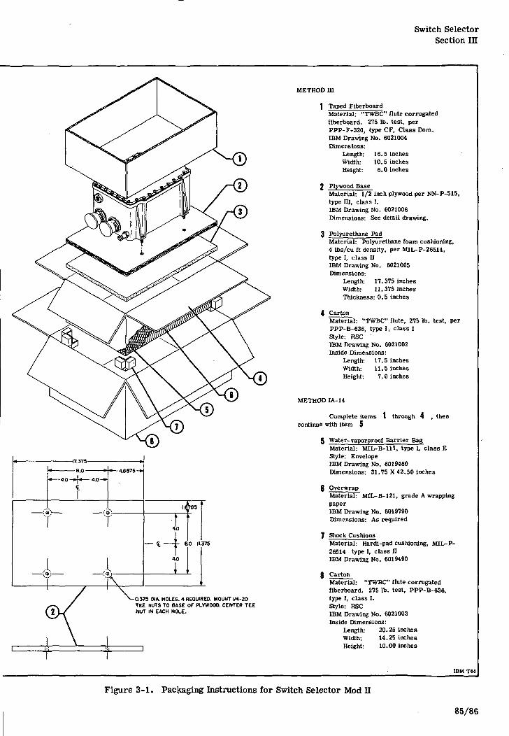
Switch SelectorSection ID
METHOD m
1 Taped FiberboardMaterial: "TWBC" flute corrugatediiberboard. 275 Ib. test, perPPP-F-320, type CF, Class Dora.IBM Drawing No. 6021004Dimensions:
Length: 16.5 inchesWidth: 10.5 inchesHeight: 6.0 inches
2 Plywood BaseMaterial: 1/2 inch plywood per NN-P-515,type m, class 1.IBM Drawing No. 6021006Dimensions: See detail drawing.
3 Polyurethane PadMaterial: Polyurethane foam cushioning,4 Ibs/cu ft density, per MIL-P-26514,type I, class HIBM Drawing No. 6021005Dimensions:
Length: 17.375 inchesWidth: 11.375 inchesThickness: 0.5 inches
4 Carton
H7.375-
-8.0- - 4.6875-H
-(o;-
4.0
-44X3
ao 11.375
-0.375 MA. HOLES. 4 REQUIRED. MOUNT 1/4-20TEE NUTS TO BASE OF PLYWOOD. CENTER TEENUT IN EACH HOLE.
Material: "TWBC" flute, 275 to. test, perPPP-B-636, type I, class IStyle: RSCIBM Drawing No. 6021002Inside Dimensions:
Length: 17.5 inchesWidth: 11.5 inchesHeight: 7.0 inches
METHOD IA-14
Complete items 1 through 4 , thencontinue with item 5
5 Water-vaporproof Barrier BagMaterial: M1L-B-117, type I, class EStyle: EnvelopeIBM Drawing No. 6019460Dimensions: 31.75 X 42.50 inches
( OverwrapMaterial: MIL-B-121, grade A wrappingpaperIBM Drawing No. 6019790Dimensions: As required
7 Shock CushionsMaterial: Hardi-pad cushioning, MIL-P-26514 type I, class nIBM Drawing No. 6019490
g CartonMaterial: "TWBC" flute corrugatedfiberboard. 275 Ib. test, PPP-B-636,type I, class I.Style: RSCIBM Drawing No. 6021003Inside Dimensions:
Length: 20.25 inchesWidth: 14.25 inches
1 if, .••'. 11 1IBM T44
Figure 3-1. Packaging Instructions for Switch Selector Mod II
85/86
Switch SelectorSection IV
SECTION IV
PREVENTIVE MAINTENANCE AND REPAIR
4-1 PREVENTIVE MAINTENANCE (Not Applicable)
4-2 REPAIR
All repairs to the Switch Selector will beaccomplished by component replacement. If failureanalysis determines repair is possible, the componentshall be returned to the manufacturer for repair.
87/88
Prill 18$ is USA
Space Systems CenterHuntsville, Alabama


![P23-DTSC DECIMAL POINT SELECTOR SWITCH … (ASA)… · DECIMAL POINT SELECTOR SWITCH – Used for round-up [ ] , round-off [5/4], ... pembulatan ke bawah [ ] terhadap digit desimal](https://img.pdfslide.us/doc/110x75/5b0a8b487f8b9a0b0f8bd986/p23-dtsc-decimal-point-selector-switch-asadecimal-point-selector-switch-used.jpg)