Embed Size (px)
Citation preview
IBM PCB Symposium
© 2009 IBM Corporation
IBM Laminate Study Group Lead-Free Laminate Robustness
Brett Krull, Dept FM2
Nov 18, 2009
IBM PCB Symposium
© 2009 IBM Corporation2 10-Dec-09
Agenda
Introductions
Laminate Robustness Background
Qualification Methods
Contributing Factors
Past Work on Laminate Characterization
Planned Collaboration with Dr. Ray Pearson
IBM PCB Symposium
© 2009 IBM Corporation3 10-Dec-09
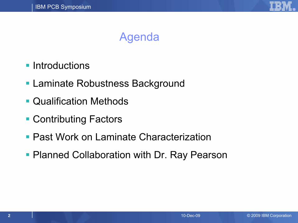
IBM Laminate Study Group
Johannes Windeln – ISC, Technical Procurement
Mark Sherwood – IBM Research
Joe Kuczynski – STG, Materials and Process Engineering
Dylan Boday – STG, Materials and Process Engineering
Brett Krull – ISC, PCB Engineering
Multiple other IBM, Academic, and Industry Involvement
IBM PCB Symposium
© 2009 IBM Corporation4 10-Dec-09
Laminate Robustness
Increasing reflow temperatures present new challenges in PCB reliability
–
Elevate “conventional”
reliability risks
–
Exceed material thermo-mechanical limits (conventional FR4)
Concerns compounded by the need for higher technologies–
Superior electrical property requirements
–
Increasingly demanding physical PCB designs
Field and manufacturing failure risk increases–
Primary concern is laminate cracking
–
Other concerns include CAF, copper integrity, and “pad cratering”
IBM PCB Symposium
© 2009 IBM Corporation5 10-Dec-09
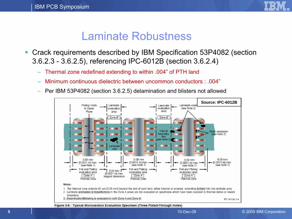
Laminate RobustnessCrack requirements described by IBM Specification 53P4082 (section 3.6.2.3 - 3.6.2.5), referencing IPC-6012B (section 3.6.2.4)
–
Thermal zone redefined extending to within .004”
of PTH land
–
Minimum continuous dielectric between uncommon conductors : .004”
–
Per IBM 53P4082 (section 3.6.2.5) delamination
and blisters not allowed
Source: IPC-6012B
IBM PCB Symposium
© 2009 IBM Corporation6 10-Dec-09
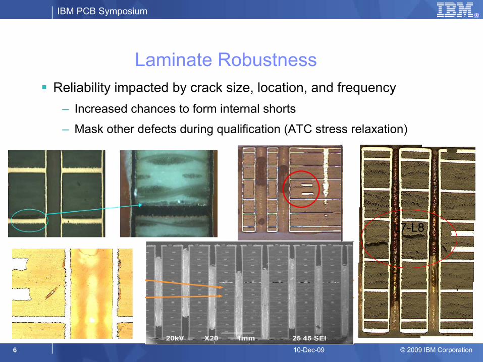
Laminate RobustnessReliability impacted by crack size, location, and frequency
–
Increased chances to form internal shorts
–
Mask other defects during qualification (ATC stress relaxation)
L7-L8
IBM PCB Symposium
© 2009 IBM Corporation7 10-Dec-09
Current Qualification Methods
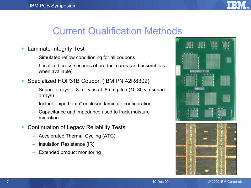
Laminate Integrity Test–
Simulated reflow conditioning for all coupons
–
Localized cross-sections of product cards (and assemblies when available)
Specialized HOP31B Coupon (IBM PN 42R8302)–
Square arrays of 8-mil vias at .8mm pitch (10-30 via square arrays)
–
Include “pipe bomb”
enclosed laminate configuration
–
Capacitance and impedance used to track moisture migration
Continuation of Legacy Reliability Tests–
Accelerated Thermal Cycling (ATC)
–
Insulation Resistance (IR)
–
Extended product monitoring
IBM PCB Symposium
© 2009 IBM Corporation8 10-Dec-09
Contributing FactorsCard Thickness
–
Thicker cards more susceptible to crack formation–
Designs trending upward–
High temperature cards up to .160”
thick planned for next 1-2 years
Via-to-via pitch–
Tighter pitch more prone to crack formation–
Designs trending downward –
now encountering sub .8mm pitch
Copper Weight–
Higher copper weights more prone to crack formation –
Design dependent
IBM PCB Symposium
© 2009 IBM Corporation9 10-Dec-09
Contributing FactorsMoisture Content
–
Higher moisture content adversely affects reflow performance–
Moisture uptake unavoidable during wet manufacturing processes–
Baking provides an acceptable solution within limits•
Laminate absorbs moisture at ambient –
special packaging required•
Process variability results in some degree of moisture variability
Material Properties–
Some material chemistries unsuitable to high temperature reflow•
Bulk material limitations•
Material interface limitations (resin:glass
interface)–
Material additives (fillers) may improve material survivability–
Better understanding needed to evaluate new materials–
Main target area of Laminate Study Group
IBM PCB Symposium
© 2009 IBM Corporation10 10-Dec-09
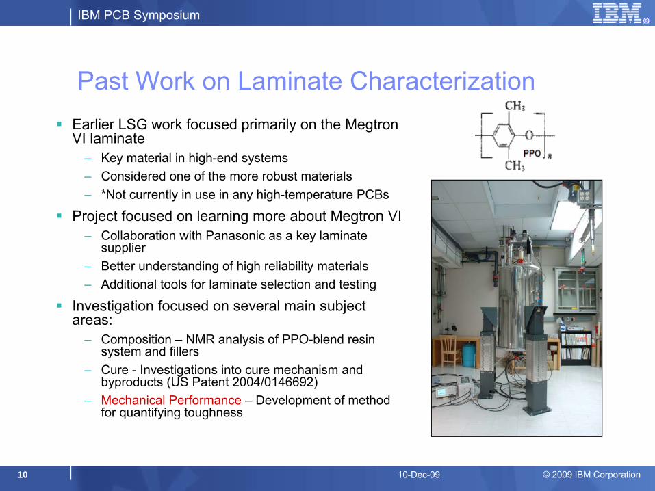
Past Work on Laminate Characterization Earlier LSG work focused primarily on the MegtronVI laminate
–
Key material in high-end systems–
Considered one of the more robust materials–
*Not currently in use in any high-temperature PCBs
Project focused on learning more about Megtron VI–
Collaboration with Panasonic as a key laminate supplier
–
Better understanding of high reliability materials–
Additional tools for laminate selection and testing
Investigation focused on several main subject areas:
–
Composition –
NMR analysis of PPO-blend resin system and fillers
–
Cure -
Investigations into cure mechanism and byproducts (US Patent 2004/0146692)
–
Mechanical Performance
–
Development of method for quantifying toughness
IBM PCB Symposium
© 2009 IBM Corporation11 10-Dec-09
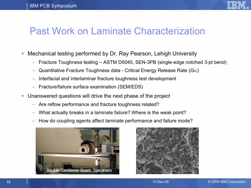
Past Work on Laminate Characterization
Mechanical testing performed by Dr. Ray Pearson, Lehigh University–
Fracture Toughness testing –
ASTM D5045, SEN-3PB (single-edge notched 3-pt bend)
–
Quantitative Fracture Toughness data -
Critical Energy Release Rate (GIC)
–
Interfacial and interlaminar
fracture toughness test development
–
Fracture/failure surface examination (SEM/EDS)
Unanswered questions will drive the next phase of the project–
Are reflow performance and fracture toughness related?
–
What actually breaks in a laminate failure? Where is the weak point?
–
How do coupling agents affect laminate performance and failure mode?
IBM PCB Symposium
© 2009 IBM Corporation12 10-Dec-09
Planned Collaboration with Ray Pearson
Continue to gather fracture toughness data–
Refine interlaminar
fracture toughness measurement method
–
Gather fracture toughness data for multiple resin systems
–
Investigate whether a relationship exists between GIC
and reflow performance
Investigate role of silane coupling agent on laminate performance–
Conduct flow microcalorimetry
to investigate resin’s ability to adsorb onto silane
–
Investigate silane
coupling agent surface energy
Identify interfacial fracture failure mode–
Determine which material surfaces are failing
–
Investigate impact of coupling agent on failure mode
Develop method to test resin-fiber matrix adhesion
IBM PCB Symposium
© 2009 IBM Corporation13 10-Dec-09
Questions?
IBM PCB Symposium
© 2009 IBM Corporation14 10-Dec-09
Back-up
IBM PCB Symposium
© 2009 IBM Corporation15 10-Dec-09
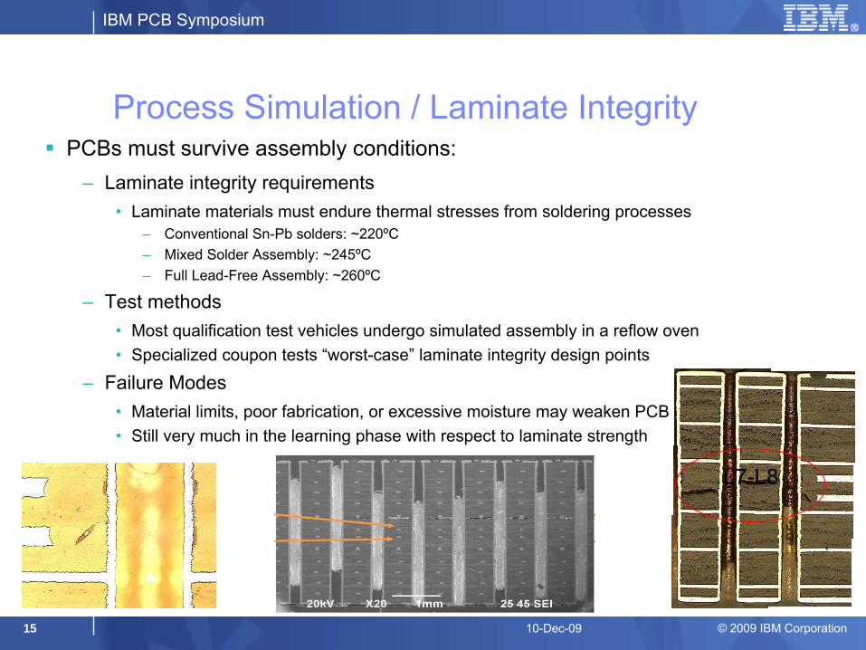
PCBs must survive assembly conditions:–
Laminate integrity requirements•
Laminate materials must endure thermal stresses from soldering processes–
Conventional Sn-Pb
solders: ~220ºC–
Mixed Solder Assembly: ~245ºC–
Full Lead-Free Assembly: ~260ºC
–
Test methods•
Most qualification test vehicles undergo simulated assembly in a
reflow oven•
Specialized coupon tests “worst-case”
laminate integrity design points
–
Failure Modes•
Material limits, poor fabrication, or excessive moisture may weaken PCB•
Still very much in the learning phase with respect to laminate strength
Process Simulation / Laminate Integrity
L7-L8
IBM PCB Symposium
© 2009 IBM Corporation16 10-Dec-09
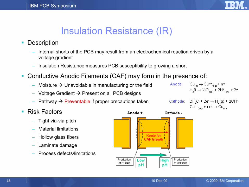
Insulation Resistance (IR)Description
–
Internal shorts of the PCB may result from an electrochemical reaction driven by a voltage gradient
–
Insulation Resistance measures PCB susceptibility to growing a short
Conductive Anodic Filaments (CAF) may form in the presence of:–
Moisture Unavoidable in manufacturing or the field
–
Voltage Gradient Present on all PCB designs
–
Pathway Preventable if proper precautions taken
Risk Factors–
Tight via-via pitch
–
Material limitations
–
Hollow glass fibers
–
Laminate damage
–
Process defects/limitations
IBM PCB Symposium
© 2009 IBM Corporation17 10-Dec-09
IR ContinuedTest conditions and requirements
–
Simulated assembly and ship shock performed on new parts
–
Parts tested in T&H chambers 50ºC / 80% RH
–
15V bias applied (~3x relevant application voltage)
–
1 Megohm
current limiting resistor protects fragile CAF filament (100 μA max)
–
Resistance measured intermittently. Failure condition is R < 100
Megohms
–
Requirements drawn from experimentally determined acceleration models•
I, P, X Series and Storage Servers: 300 Hours•
Z Series : 600 Hours
Common failure modes–
Via-to-Via Resin/glass separation, hollow glass fibers, poor resin fill
–
Via-to-Plane Contaminants during lamination, laminate damage
–
Plane-to-Plane Resin gaps in single ply materials, laminate damage
IBM PCB Symposium
© 2009 IBM Corporation18 10-Dec-09
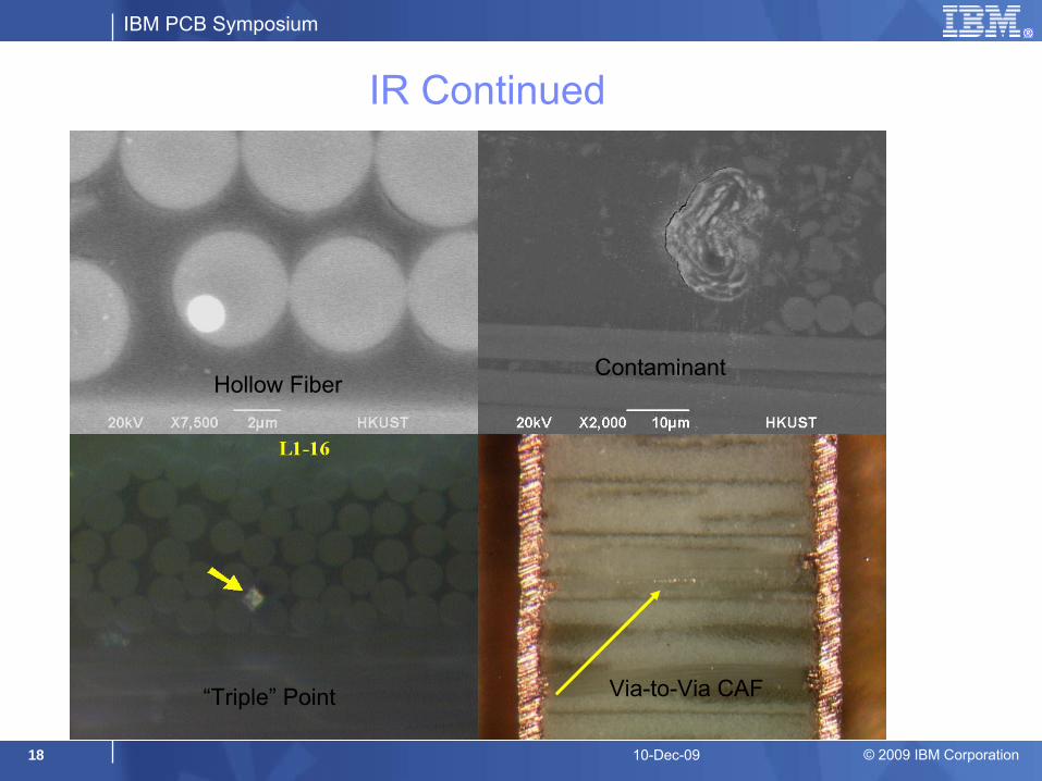
IR Continued
Hollow Fiber
“Triple” Point
Contaminant
Via-to-Via CAF