Embed Size (px)
Citation preview

This is information on a product in full production.
June 2013 DocID13236 Rev 9 1/28
STVM100
I2C LCD/e-paper VCOM calibrator
Datasheet - production data
Features
• I2C interface, slave address: 1001111
• 7-bit adjustable sink current output
• 2.25 V to 3.6 V logic supply voltage VDD
• AVDD operating voltages
– 4.5 V to 20 V for VDD from 2.6 V to 3.6 V
– 4.5 V to 13 V for VDD from 2.25 V to 3.6 V
• EEPROM for storing the optimum VCOM setting
• Guaranteed monotonic output over operating range
• 400 kHz maximum interface bus speed
• Operating temperature: –40 °C to 85 °C
• Available in an 8-pin 3 mm x 3 mm TDFN8 or 3 mm x 3 mm TSSOP8 package
Applications
• TFT-LCD panels
• e-paper and e-book displays
Description
The STVM100 is a programmable VCOM adjustment solution for thin-film transistor (TFT) liquid-crystal displays (LCDs) to remove “flickers”. It is also used in e-paper and e-book applications to avoid the “ghosting” effect (residual pixels after display refresh). It can replace a mechanical potentiometer, so that the factory operator can physically view the front screen when performing the VCOM adjustment. This significantly reduces labor costs, increases reliability, and enables automation.
The STVM100 provides a digital I2C interface to control the sink current output (IOUT). This output drives an external resistive voltage divider, which can then be applied to an external VCOM buffer. Three external resistors R1, R2, and RSET determine the highest and lowest value of the VCOM. An increase in the output sink current will lower the voltage on the external divider so that the VCOM can be adjusted by 128 steps within this range. Once the desired VCOM setting is achieved, it can be stored in the internal EEPROM that will be automatically recalled during each power-up.
The STVM100 is available in an 8-pin, 3 mm x 3 mm TDFN8 or 3 mm x 3 mm TSSOP8 package.
TDFN8 (3 mm x 3 mm) (DC)
TSSOP8 (3 mm x 3 mm) (DS)
Table 1. Device summary
Order code Optimum temperature range Package Packing
STVM100DC6F –40 °C to 85 °C TDFN8 ECOPACK® package, tape and reel
STVM100DS6F –40 °C to 85 °C TSSOP8 ECOPACK® package, tape and reel
www.st.com
DocID13236 Rev 9 3/28
STVM100 Contents
3
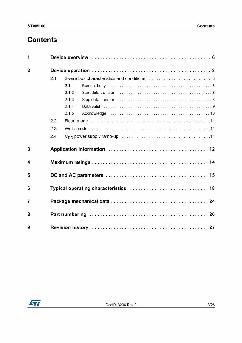
Contents
1 Device overview . . . . . . . . . . . . . . . . . . . . . . . . . . . . . . . . . . . . . . . . . . . . 6
2 Device operation . . . . . . . . . . . . . . . . . . . . . . . . . . . . . . . . . . . . . . . . . . . . 8
2.1 2-wire bus characteristics and conditions . . . . . . . . . . . . . . . . . . . . . . . . . . 8
2.1.1 Bus not busy . . . . . . . . . . . . . . . . . . . . . . . . . . . . . . . . . . . . . . . . . . . . . . 8
2.1.2 Start data transfer . . . . . . . . . . . . . . . . . . . . . . . . . . . . . . . . . . . . . . . . . . 8
2.1.3 Stop data transfer . . . . . . . . . . . . . . . . . . . . . . . . . . . . . . . . . . . . . . . . . . 8
2.1.4 Data valid . . . . . . . . . . . . . . . . . . . . . . . . . . . . . . . . . . . . . . . . . . . . . . . . . 9
2.1.5 Acknowledge . . . . . . . . . . . . . . . . . . . . . . . . . . . . . . . . . . . . . . . . . . . . . 10
2.2 Read mode . . . . . . . . . . . . . . . . . . . . . . . . . . . . . . . . . . . . . . . . . . . . . . . . .11
2.3 Write mode . . . . . . . . . . . . . . . . . . . . . . . . . . . . . . . . . . . . . . . . . . . . . . . . .11
2.4 VDD power supply ramp-up . . . . . . . . . . . . . . . . . . . . . . . . . . . . . . . . . . . .11
3 Application information . . . . . . . . . . . . . . . . . . . . . . . . . . . . . . . . . . . . . 12
4 Maximum ratings . . . . . . . . . . . . . . . . . . . . . . . . . . . . . . . . . . . . . . . . . . . 14
5 DC and AC parameters . . . . . . . . . . . . . . . . . . . . . . . . . . . . . . . . . . . . . . 15
6 Typical operating characteristics . . . . . . . . . . . . . . . . . . . . . . . . . . . . . 18
7 Package mechanical data . . . . . . . . . . . . . . . . . . . . . . . . . . . . . . . . . . . . 24
8 Part numbering . . . . . . . . . . . . . . . . . . . . . . . . . . . . . . . . . . . . . . . . . . . . 26
9 Revision history . . . . . . . . . . . . . . . . . . . . . . . . . . . . . . . . . . . . . . . . . . . 27
List of tables STVM100
4/28 DocID13236 Rev 9
List of tables
Table 1. Device summary . . . . . . . . . . . . . . . . . . . . . . . . . . . . . . . . . . . . . . . . . . . . . . . . . . . . . . . . . . 1Table 2. Pin names and functions . . . . . . . . . . . . . . . . . . . . . . . . . . . . . . . . . . . . . . . . . . . . . . . . . . . 6Table 3. Bit P read and write mode values . . . . . . . . . . . . . . . . . . . . . . . . . . . . . . . . . . . . . . . . . . . . 11Table 4. Absolute maximum ratings . . . . . . . . . . . . . . . . . . . . . . . . . . . . . . . . . . . . . . . . . . . . . . . . . 14Table 5. Operating and AC measurement conditions. . . . . . . . . . . . . . . . . . . . . . . . . . . . . . . . . . . . 15Table 6. Capacitances . . . . . . . . . . . . . . . . . . . . . . . . . . . . . . . . . . . . . . . . . . . . . . . . . . . . . . . . . . . 15Table 7. DC and AC characteristics . . . . . . . . . . . . . . . . . . . . . . . . . . . . . . . . . . . . . . . . . . . . . . . . . 16Table 8. AC characteristics. . . . . . . . . . . . . . . . . . . . . . . . . . . . . . . . . . . . . . . . . . . . . . . . . . . . . . . . 17Table 9. TDFN8 3 x 3 x 0.75 mm, pitch 0.65, package mechanical data . . . . . . . . . . . . . . . . . . . . . 24Table 10. TSSOP8 – 8-lead, thin shrink small outline, 3 mm x 3 mm, mech. data. . . . . . . . . . . . . . . 25Table 11. Ordering information scheme . . . . . . . . . . . . . . . . . . . . . . . . . . . . . . . . . . . . . . . . . . . . . . . 26Table 12. Document revision history . . . . . . . . . . . . . . . . . . . . . . . . . . . . . . . . . . . . . . . . . . . . . . . . . 27

DocID13236 Rev 9 5/28
STVM100 List of figures
5
List of figures
Figure 1. Logic diagram . . . . . . . . . . . . . . . . . . . . . . . . . . . . . . . . . . . . . . . . . . . . . . . . . . . . . . . . . . . . 6Figure 2. Connections diagram . . . . . . . . . . . . . . . . . . . . . . . . . . . . . . . . . . . . . . . . . . . . . . . . . . . . . . 7Figure 3. Block diagram . . . . . . . . . . . . . . . . . . . . . . . . . . . . . . . . . . . . . . . . . . . . . . . . . . . . . . . . . . . . 7Figure 4. Hardware hookup . . . . . . . . . . . . . . . . . . . . . . . . . . . . . . . . . . . . . . . . . . . . . . . . . . . . . . . . . 7Figure 5. Serial bus data transfer sequence . . . . . . . . . . . . . . . . . . . . . . . . . . . . . . . . . . . . . . . . . . . . 9Figure 6. Acknowledgment sequence . . . . . . . . . . . . . . . . . . . . . . . . . . . . . . . . . . . . . . . . . . . . . . . . 10Figure 7. Read/write mode sequence . . . . . . . . . . . . . . . . . . . . . . . . . . . . . . . . . . . . . . . . . . . . . . . . 11Figure 8. R1, R2, and RSET connection . . . . . . . . . . . . . . . . . . . . . . . . . . . . . . . . . . . . . . . . . . . . . . . 12Figure 9. Bus timing requirements sequence . . . . . . . . . . . . . . . . . . . . . . . . . . . . . . . . . . . . . . . . . . 17Figure 10. VDD supply current vs. VDD . . . . . . . . . . . . . . . . . . . . . . . . . . . . . . . . . . . . . . . . . . . . . . . . 18Figure 11. AVDD supply current vs. AVDD . . . . . . . . . . . . . . . . . . . . . . . . . . . . . . . . . . . . . . . . . . . . . . 18Figure 12. VDD supply current vs. temperature . . . . . . . . . . . . . . . . . . . . . . . . . . . . . . . . . . . . . . . . . . 19Figure 13. AVDD supply current vs. temperature . . . . . . . . . . . . . . . . . . . . . . . . . . . . . . . . . . . . . . . . . 19Figure 14. IOUT error vs. temperature (STVM100 at middle scale) . . . . . . . . . . . . . . . . . . . . . . . . . . . 20Figure 15. Total unadjusted error vs. DAC setting. . . . . . . . . . . . . . . . . . . . . . . . . . . . . . . . . . . . . . . . 20Figure 16. Differential non-linearity vs. DAC setting . . . . . . . . . . . . . . . . . . . . . . . . . . . . . . . . . . . . . . 21Figure 17. Integral non-linearity vs. DAC setting . . . . . . . . . . . . . . . . . . . . . . . . . . . . . . . . . . . . . . . . . 21Figure 18. AVDD power-up response . . . . . . . . . . . . . . . . . . . . . . . . . . . . . . . . . . . . . . . . . . . . . . . . . . 22Figure 19. Full scale-up response . . . . . . . . . . . . . . . . . . . . . . . . . . . . . . . . . . . . . . . . . . . . . . . . . . . . 22Figure 20. Full scale-down response . . . . . . . . . . . . . . . . . . . . . . . . . . . . . . . . . . . . . . . . . . . . . . . . . . 23Figure 21. TDFN8 3 x 3 x 0.75 mm, pitch 0.65, package mechanical data . . . . . . . . . . . . . . . . . . . . . 24Figure 22. TSSOP8 – 8-lead, thin shrink small outline, 3 mm x 3 mm, mech. data. . . . . . . . . . . . . . . 25

Device overview STVM100
6/28 DocID13236 Rev 9
1 Device overview
Figure 1. Logic diagram
Table 2. Pin names and functions
Name Type Function
OUT AnalogAdjustable sink current output pin. (1)
See Section 3: Application information on page 12.
1. See SET pin function in this table for the maximum adjustable sink current setting.
AVDD SupplyHigh-voltage analog supply.
Bypass to GND with a 0.1 µF capacitor.
WP Input
WRITE protectection.
Active-low. To enable write operations to the DAC or to the EEPROM writing, connect to 0.7 VDD or greater. Internally pulled down by a 130 kΩ resistor.
GND Supply ground.
VDD SupplySystem power supply input.
Bypass to GND with a 0.1 µF capacitor.
SDA Input/Output I2C serial data input/output.
SCL Input I2C serial clock input.
SET Analog
Maximum sink current adjustment point.
Connect a resistor from SET to GND to set the maximum adjustable sink current of the OUT pin. The maximum adjustable sink current is equal to AVDD /20 divided by RSET (see Figure 4 on page 7).
AI12272
SDA
VDD
STVM100
GND
SCL
WP
AVDD
OUT
SET

DocID13236 Rev 9 7/28
STVM100 Device overview
27
Figure 2. Connections diagram
Figure 3. Block diagram
Figure 4. Hardware hookup
1
VDDGND
SDA
SCLAVDD
OUT SET
WP
AI12273
2
3
4
8
7
6
5
AVDD
GND
EEPROMBlock
DACI2CInterface
R
19R
+
–
VDD
SDA
SCL
OUT7
7 SET
WP
AI12274
AVDD
AVDD
VDD3.3V
RSET
R2
R1
GND
MCU
I2
C In
te
rfa
ce
0.1μF
0.1μF
+
–
VDD
SDA
SCL
VCOMSET
OUT
WP
AI12275
STVM100
Device operation STVM100
8/28 DocID13236 Rev 9
2 Device operation
The STVM100 operates as a slave device on the serial bus. Access is obtained by implementing a start condition, followed by the 7-bit slave address (1001111), and the eighth bit for READ/WRITE identification. The volatile DAC register and non-volatile EEPROM values can be read out or written in.
2.1 2-wire bus characteristics and conditions
This bus is intended for communication between different ICs. It consists of two lines:
• a bi-directional data signal (SDA).
• a clock signal (SCL).
The SDA and SCL lines must be connected to a positive supply voltage via a pull-up resistor. The following protocols have been defined:
• Data transfer may be initiated only when the bus is not busy.
• During data transfer, the data line must remain stable whenever the clock line is high.
• Changes in the data line while the clock line is high will be interpreted as control signals.
2.1.1 Bus not busy
Both data and clock lines remain high.
2.1.2 Start data transfer
A change in the data line state from high-to-low while the clock is high indicate the start condition.
2.1.3 Stop data transfer
A change in the data line state from low-to-high while the clock is high indicates the stop condition.

DocID13236 Rev 9 9/28
STVM100 Device operation
27
2.1.4 Data valid
The data on the SDA line must be stable during the high period of the clock. The high or low state of the data line can only change when the clock signal on the SCL line is low (see Figure 5). The data on the line may be changed during the clock signal low period. There is one clock pulse per bit of data.
Each data transfer is initiated with a start condition and terminated with a stop condition. The number of data bytes transferred between the start and stop conditions is not limited. The information is transmitted byte-wide and each receiver acknowledges transmission with a ninth bit.
By definition, the device that gives out a message is called “transmitter”, the device that gets the message is called “receiver”. The device that controls the message is called the “master”. The devices controlled by the master are called “slave” devices.
Figure 5. Serial bus data transfer sequence
AI00587
DATA
CLOCK
DATA LINE
STABLE
DATA VALID
START
CONDITION
CHANGE OF
DATA ALLOWED
STOP
CONDITION

Device operation STVM100
10/28 DocID13236 Rev 9
2.1.5 Acknowledge
Each byte of eight bits is followed by one acknowledge bit. This acknowledge bit is a low level signal put on the bus by the receiver, whereas the master generates an extra acknowledge-related clock pulse (see Figure 6). A slave receiver which is addressed is obliged to generate an acknowledge signal after the reception of each byte that has been clocked out of the slave transmitter.
The device that acknowledges transmissions has to pull down the SDA line during the acknowledge clock pulse in such a way, that the SDA line is a stable low during the high period of the acknowledge-related clock pulse. The setup and hold times must be taken into account. A master receiver must signal an end of transmitted data to the slave transmitter by not generating an acknowledge on the last byte that has been clocked out of the slave. In this case, the transmitter must leave the data line high to enable the master to generate the stop condition.
Figure 6. Acknowledgment sequence
AI00601
DATA OUTPUT
BY RECEIVER
DATA OUTPUT
BY TRANSMITTER
SCL FROM
MASTER
START
CLOCK PULSE FOR
ACKNOWLEDGEMENT
1 2 8 9
MSB LSB

DocID13236 Rev 9 11/28
STVM100 Device operation
27
2.2 Read mode
In READ mode, after the start condition, the master sets the slave address (see Figure 7). Followed by the READ/WRITE mode control bit (R/W=1) and the acknowledge bit, the value in DAC register will be transmitted and the master receiver will send an acknowledge bit to the slave transmitter. Finally the stop condition will terminate the READ operation. In READ mode, the valid data is the first 7 bits and the P bit (the eight bit) is don’t care.
2.3 Write mode
In WRITE mode the master transmits to the STVM100 slave receiver. The bus protocol is shown in Figure 7. Following the start condition and slave address, a logic '0' (R/W = 0) is placed on the bus to identify a WRITE operation. After the acknowledgement by the slave, the data will be transmitted to the slave with the 7-bit which indicates the data is valid as well as the eighth bit “P” for the register’s identification. When P = 1, the DAC register is written to, and when P = 0, the EEPROM is written to (Programming). After receiving the data, the slave will generate an acknowledge signal, then a stop condition will terminate the WRITE operation. STVM100 is pre-programmed with 80H in the EEPROM after manufacturing.
A period of tW (see Table 8) is needed for EEPROM programming. During this period, the slave will not acknowledge any WRITE operation.
The bit P values in both READ and WRITE modes are shown in Table 3.
Figure 7. Read/write mode sequence
2.4 VDD power supply ramp-up
The ramp-up from 10% VDD to 90% VDD level should be achieved in less than or equal to 10ms to ensure that the EEPROM and power-on reset circuits are synchronized, and the correct value is read from the EEPROM.
Table 3. Bit P read and write mode values
Operation P-bit value Description
READ X Don’t care
WRITE
1 DAC register WRITE
0EEPROM WRITE
(programming)
AI12276_b
1
START STOP
SDA
SCL
0 0 1 1 1 1
1 0 0 1 1 1 1
START SLAVE ADDRESS
R/W A
A
6 5 4 3 2 1 0 P
6 5 4 3 2 1 0 P
A
A STOPR/W
Application information STVM100
12/28 DocID13236 Rev 9
3 Application information
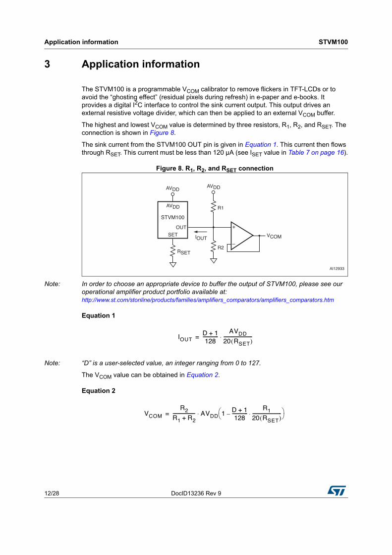
The STVM100 is a programmable VCOM calibrator to remove flickers in TFT-LCDs or to avoid the “ghosting effect” (residual pixels during refresh) in e-paper and e-books. It provides a digital I2C interface to control the sink current output. This output drives an external resistive voltage divider, which can then be applied to an external VCOM buffer.
The highest and lowest VCOM value is determined by three resistors, R1, R2, and RSET. The connection is shown in Figure 8.
The sink current from the STVM100 OUT pin is given in Equation 1. This current then flows through RSET. This current must be less than 120 µA (see ISET value in Table 7 on page 16).
Figure 8. R1, R2, and RSET connection
Note: In order to choose an appropriate device to buffer the output of STVM100, please see our operational amplifier product portfolio available at:http://www.st.com/stonline/products/families/amplifiers_comparators/amplifiers_comparators.htm
Equation 1
Note: “D” is a user-selected value, an integer ranging from 0 to 127.
The VCOM value can be obtained in Equation 2.
Equation 2
AVDD
IOUT
VCOM
AVDD
RSET
R1
R2
SET
STVM100
+
–
AVDD
OUT
AI12933
IOUT
D 1+
128
--------------
AVDD
20 RSET
( )--------------------------⋅=
VCOM
R2
R1
R2
+
-------------------- AVDD
1D 1+
128
--------------
R1
20 RSET
( )--------------------------⋅–
⋅=

DocID13236 Rev 9 13/28
STVM100 Application information
27
If the user-selected value is 0 (zero scale), the minimum current is sunk. The maximum VCOM value is obtained in Equation 3.
Equation 3
If the user-selected value is 127 (full scale), the maximum current is sunk and the minimum VCOM value is obtained in Equation 4.
Equation 4
During operation, the VCOM(max) and VCOM(min) range is set, based on different TFT-LCD processes.The R1 value is given based on the acceptable power loss from the AVDD supply rail. Using Equation 3 and Equation 4, the R2 and RSET values can be calculated. If RSET is put into Equation 1 on page 12 and maximum IOUT ≥ 120 µA, then R1 should be increased.
VCOM max( )
R2
R1
R2
+
-------------------- AVDD
11
128
----------
R1
20 RSET
( )--------------------------⋅–
⋅=
VCOM min( )
R2
R1
R2
+
-------------------- AVDD
1
R1
20 RSET
( )--------------------------–
⋅=
Maximum ratings STVM100
14/28 DocID13236 Rev 9
4 Maximum ratings
Stressing the device above the ratings listed in the absolute maximum ratings table may cause permanent damage to the device. These are stress ratings only and operation of the device at these or any other conditions above those indicated in the operating sections of this specification is not implied. Exposure to absolute maximum rating conditions for extended periods may affect device reliability. Refer also to the STMicroelectronics SURE Program and other relevant quality documents.
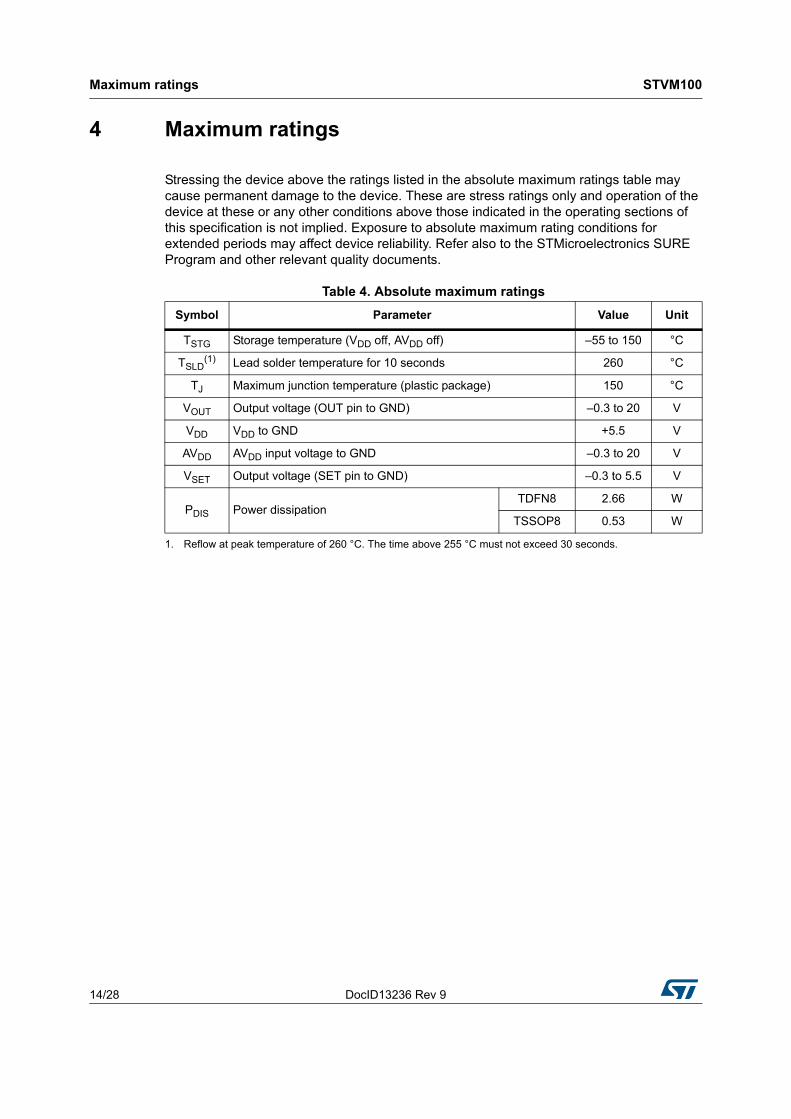
Table 4. Absolute maximum ratings
Symbol Parameter Value Unit
TSTG Storage temperature (VDD off, AVDD off) –55 to 150 °C
TSLD(1)
1. Reflow at peak temperature of 260 °C. The time above 255 °C must not exceed 30 seconds.
Lead solder temperature for 10 seconds 260 °C
TJ Maximum junction temperature (plastic package) 150 °C
VOUT Output voltage (OUT pin to GND) –0.3 to 20 V
VDD VDD to GND +5.5 V
AVDD AVDD input voltage to GND –0.3 to 20 V
VSET Output voltage (SET pin to GND) –0.3 to 5.5 V
PDIS Power dissipationTDFN8 2.66 W
TSSOP8 0.53 W

DocID13236 Rev 9 15/28
STVM100 DC and AC parameters
27
5 DC and AC parameters
This section summarizes the operating measurement conditions, and the dc and ac characteristics of the device. The parameters in the DC and AC characteristics tables that follow, are derived from tests performed under the measurement conditions summarized in Table 5. Designers should check that the operating conditions in their circuit match the operating conditions when relying on the quoted parameters.
Table 5. Operating and AC measurement conditions
Parameter Conditions Unit
VDD supply voltage 2.25 to 3.6 V
VDD EEPROM programming supply voltage 2.25 to 3.6 V
AVDD reference voltage 4.5 to 20 V
Ambient operating temperature (TA) –40 to 85 °C
Table 6. Capacitances
Symbol Parameter(1)(2)
1. Effective capacitance measured with power supply at 3 V. Sampled only, not 100% tested.
2. At 25 °C, f = 1 MHz.
Min Max Unit
Cb Bus capacitive load 400 pF
CSDA Capacitance on SDA 10 pF
CS Capacitance on SCLWP = 0 10 pF
WP = 1 22 pF

DC and AC parameters STVM100
16/28 DocID13236 Rev 9
Table 7. DC and AC characteristics
Sym Description Test condition(1)
1. Valid for ambient operating temperature: TA = –40 to 85 °C; VDD = 3 V; AVDD = 10 V; typical TA = 25 °C; OUT = 1/2AVDD; RSET = 24.9 kΩ (except where noted).
Min Typ Max Unit
VDD
Supply voltage 2.25 3.6 V
EEPROM programming supply voltage
2.25 3.6 V
IDD(2)
2. Simulated maximum current draw when Programming EEPROM is 23 mA; should be considered when designing a power supply.
VDD supply current 50 µA
AVDD Analog supply voltageVDD = 2.6 V to 3.6 V 4.5 20 V
VDD = 2.25 V to 3.6 V 4.5 13 V
IAVDD(3)
3. Tested at AVDD = 20 V.
AVDD supply current 25 µA
SETVR SET voltage resolution 7 Bits
SETDNSET differential nonlinearity
Monotonic over temperature
±1 LSB
SETZSE SET zero scale error ±2 LSB
SETFSE SET full scale error ±8 LSB
ISET(4)
4. A typical Current of 20 µA is calculated using AVDD = 10 V and RSET = 24.9 kΩ. The maximum suggested SET current should be 120 µA.
SET current Through RSET 120 µA
SETERSET external resistance
To GND, AVDD = 20 V 10 200 kΩ
To GND, AVDD = 4.5 V 2.25 45 kΩ
AVDD to SET
AVDD to SET voltage attenuation(5)
5. Simulated and determined via design and NOT directly tested.
20 V/V
OUTST OUT settling time 8 µs
VOUT OUT voltageVSET + 0.5V
13 V
SETVD SET voltage drift(5) T = 25 °C to 55 °C <10 mV
VIHSDA, SCL, WP input logic high
0.7 VDD V
VILSDA, SCL, WP input logic low
0.3VDD V
SDA, SCL hysteresis(5) 0.22 VDD V
IIL(WPN) WPN input current 15 25 35 µA
VOL(s)SDA, SCL output logic low
At 3 mA 0.4 V

DocID13236 Rev 9 17/28
STVM100 DC and AC parameters
27
Figure 9. Bus timing requirements sequence
Table 8. AC characteristics
Sym Description Test Condition(1)
1. Valid for ambient operating temperature: TA = –40 to 85 °C; VDD = 3.0 V to 3.6 V; AVDD = 10 V; OUT = 1/2AVDD; RSET = 24.9 kΩ (except where noted, see Figure 9).
Min Typ Max Unit
fSCL SCL clock frequency 0 400 kHz
tLOW Clock low period 1.3 µs
tHIGH Clock high period 0.6 µs
tSU:DAT Data setup time 100 ns
tHD:DAT Data hold time 0 900 ns
tR SDA and SCL rise time Dependent on load (see Table 6 on page 15)
20 + 0.1 Cb
300 ns
tF SDA and SCL fall time 300 ns
tBUF
Bus free time before new transmission can start
1.3 µs
tDSPI2C spike rejection filter pulse width
0 50 ns
tSU:STARepeated start condition setup time
0.6 µs
tHD:STARepeated start condition hold time
0.6 µs
tSU:STOStop condition setup time
0.6 µs
tW WRITE cycle time 100 ms
AI00589
SDA
PtSU:STOtSU:STA
tHD:STA
SR
SCL
tSU:DAT
tF
tHD:DAT
tR
tHIGH
tLOW
tHD:STAtBUF
SP

Typical operating characteristics STVM100
18/28 DocID13236 Rev 9
6 Typical operating characteristics
Typical operating characteristics for the STVM100 are TA = 25 °C, VDD = 3 V, AVDD = 10 V, OUT = 1/2AVDD, and RSET = 24.9 kΩ except where noted.
Figure 10. VDD supply current vs. VDD
Figure 11. AVDD supply current vs. AVDD
AI13362
24
24.5
25
25.5
26
26.5
27
27. 5
.2. 2 2.4 2.6 2.8 3.0 3.2 3.4 3.6
ID
D (μ
A)
VDD
(V)
AI13363
0
1
2
3
4
5
6
7
8
9
10
4.5 6 7.5 9 10.5 12 13.5 15 16.5 18 19.5
IA
VD
D (μ
A)
AVDD
(V)

DocID13236 Rev 9 19/28
STVM100 Typical operating characteristics
27
Figure 12. VDD supply current vs. temperature
Figure 13. AVDD supply current vs. temperature
AI13364
15
20
25
30
35
-40 -30 -20 -10 0 10 20 30 40 50 60 70 80 90
Temperature°C
ID
D (μ
A)
AI13365
4.5
4.55
4.6
4.65
4.7
4.75
4.8
4.85
4.9
4.95
-40 -30 -20 -10 0 10 20 30 40 50 60 70 80 90
IA
VD
D (μ
A)
Temperature°C

Typical operating characteristics STVM100
20/28 DocID13236 Rev 9
Figure 14. IOUT error vs. temperature (STVM100 at middle scale)
Figure 15. Total unadjusted error vs. DAC setting
AI13366
0
0.01
0.02
0.03
0.04
0.05
0.06
-40 -20 0 20 40 60 80
IO
UT
e
rro
r (L
SB
)
Temperature°C
AI13367
0.01
0.012079
0.014158
0.016237
0.018316
0.020395
1 17 33 49 65 81 97 113
To
ta
l u
na
dju
ste
d e
rro
r (L
SB
)
DAC setting (decimal)
0.022474

DocID13236 Rev 9 21/28
STVM100 Typical operating characteristics
27
Figure 16. Differential non-linearity vs. DAC setting
Figure 17. Integral non-linearity vs. DAC setting
AI13368
-0.2
-0.15
-0.1
-0.05
0
0.05
0.1
0.15
0.2
1 17 33 49 65 81 97 113
Diffe
re
ntia
l n
on
-lin
ea
rity (L
SB
)
DAC setting (decimal)
AI13369
-0.3
-0.2
-0.1
0
0.1
0.2
0.3
1 17 33 49 65 81 97 113
Integra
l non-linearity (LS
B)
DAC setting (decimal)

Typical operating characteristics STVM100
22/28 DocID13236 Rev 9
Figure 18. AVDD power-up response
Figure 19. Full scale-up response
5ms/DIVAVDD: 5V/DIV, VDD: 5V/DIV, VOUT: 1V/DIV, VSET: 1V/DIV
20µs/DIVSCL: 5V/DIV, SDA: 5V/DIV, VOUT: 1V/DIV, VSET: 1V/DIV

DocID13236 Rev 9 23/28
STVM100 Typical operating characteristics
27
Figure 20. Full scale-down response
20µs/DIVSCL: 5V/DIV, SDA: 5V/DIV, VOUT: 1V/DIV, VSET: 1V/DIV

Package mechanical data STVM100
24/28 DocID13236 Rev 9
7 Package mechanical data
In order to meet environmental requirements, ST offers these devices in different grades of ECOPACK® packages, depending on their level of environmental compliance. ECOPACK® specifications, grade definitions and product status are available at: www.st.com. ECOPACK® is an ST trademark.
Figure 21. TDFN8 3 x 3 x 0.75 mm, pitch 0.65, package mechanical data
Note: Drawing is not to scale.
0.08
E2
D2
L1
8
b
EZ_ME
e
D
E
A
A3 A1
Table 9. TDFN8 3 x 3 x 0.75 mm, pitch 0.65, package mechanical data
Symmm inches
Typ Min Max Typ Min Max
A 0.75 0.70 0.80 0.0295 0.0276 0.0315
A1 0.02 0.00 0.05 0.0008 0.0000 0.0020
A3 0.20 0.0079
b 0.30 0.25 0.35 0.0118 0.0098 0.0138
D 3.00 0.1181
D2 2.38 2.23 2.48 0.0937 0.0878 0.0976
E 3.00 0.1181
E2 1.64 1.49 1.74 0.0646 0.0587 0.0685
e 0.65 – – 0.0256 – –
L 0.40 0.30 0.50 0.0157 0.0118 0.0197
DocID13236 Rev 9 25/28
STVM100 Package mechanical data
27
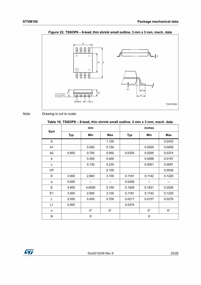
Figure 22. TSSOP8 – 8-lead, thin shrink small outline, 3 mm x 3 mm, mech. data
Note: Drawing is not to scale.
TSSOP8BM
1
8
CP
c
L
EE1
D
A2A
eb
4
5
A1
L1
Table 10. TSSOP8 – 8-lead, thin shrink small outline, 3 mm x 3 mm, mech. data
Symmm inches
Typ Min Max Typ Min Max
A 1.100 0.0433
A1 0.050 0.150 0.0020 0.0059
A2 0.850 0.750 0.950 0.0335 0.0295 0.0374
b 0.250 0.400 0.0098 0.0157
c 0.130 0.230 0.0051 0.0091
CP 0.100 0.0039
D 3.000 2.900 3.100 0.1181 0.1142 0.1220
e 0.650 – – 0.0256 – –
E 4.900 4.6500 5.150 0.1929 0.1831 0.2028
E1 3.000 2.900 3.100 0.1181 0.1142 0.1220
L 0.550 0.400 0.700 0.0217 0.0157 0.0276
L1 0.950 0.0374
α 0° 6° 0° 6°
N 8 8

Part numbering STVM100
26/28 DocID13236 Rev 9
8 Part numbering
Table 11. Ordering information scheme
For other options, or for more information on any aspect of this device, please contact the ST sales office nearest you.
Example: STVM100 DC 6 F
Device type
STVM100, VCOM calibrator with 7-bit DAC and I2C interface
Package
DC = TDFN8
DS = TSSOP8
Temperature range
6 = –40 to 85°C
Shipping method
E = ECOPACK® package, tubes
F = ECOPACK® package, tape & reel

DocID13236 Rev 9 27/28
STVM100 Revision history
27
9 Revision history
Table 12. Document revision history
Date Revision Changes
09-May-2006 1 Initial release.
14-Jul-2006 2 Graphical and textual updates
08-Nov-2006 3
Document status upgraded to Preliminary Data; changed the wording of Input function to include ‘WRITE operations’ instead of ‘programming’ in Table 2: Pin names and functions; deleted some bracketed text and modified the P bit function in Section 2.2: Read mode; ensured that all of Equation 2 and Equation 3 were visible; amalgamated 2 cells containing the same information (VDD) in Table 7: DC and AC characteristics; deleted footnotes 2 and 3 of Table 8: AC characteristics; updated package mechanical information in Figure 21, Table 9, and Table 10.
12-Feb-2007 4
Reformatted inside cover page according to new template; renamed section 1 Device overview and section 2 Device operation; deleted Signal names table; moved and renamed Table 2: Pin names and functions, addedSection 6: Typical operating characteristics and Figure 10 to Figure 20.
20-Apr-2007 5 Value added in Section 2.3: Write mode.
24-Jul-2007 6 Document status upgraded to full datasheet.
04-Nov-2009 7Added “Note” to Figure 8; updated footnote of Table 4; minor textual changes.
09-Dec-2009 8Updated title of datasheet, Applications, Description, and Section 3: Application information.
07-Jun-2013 9Replaced order code STVM100DC6E with STVM100DC6F in Table 1: Device summary

STVM100
28/28 DocID13236 Rev 9
Please Read Carefully:
Information in this document is provided solely in connection with ST products. STMicroelectronics NV and its subsidiaries (“ST”) reserve theright to make changes, corrections, modifications or improvements, to this document, and the products and services described herein at anytime, without notice.
All ST products are sold pursuant to ST’s terms and conditions of sale.
Purchasers are solely responsible for the choice, selection and use of the ST products and services described herein, and ST assumes noliability whatsoever relating to the choice, selection or use of the ST products and services described herein.
No license, express or implied, by estoppel or otherwise, to any intellectual property rights is granted under this document. If any part of thisdocument refers to any third party products or services it shall not be deemed a license grant by ST for the use of such third party productsor services, or any intellectual property contained therein or considered as a warranty covering the use in any manner whatsoever of suchthird party products or services or any intellectual property contained therein.
UNLESS OTHERWISE SET FORTH IN ST’S TERMS AND CONDITIONS OF SALE ST DISCLAIMS ANY EXPRESS OR IMPLIEDWARRANTY WITH RESPECT TO THE USE AND/OR SALE OF ST PRODUCTS INCLUDING WITHOUT LIMITATION IMPLIEDWARRANTIES OF MERCHANTABILITY, FITNESS FOR A PARTICULAR PURPOSE (AND THEIR EQUIVALENTS UNDER THE LAWSOF ANY JURISDICTION), OR INFRINGEMENT OF ANY PATENT, COPYRIGHT OR OTHER INTELLECTUAL PROPERTY RIGHT.
ST PRODUCTS ARE NOT AUTHORIZED FOR USE IN WEAPONS. NOR ARE ST PRODUCTS DESIGNED OR AUTHORIZED FOR USEIN: (A) SAFETY CRITICAL APPLICATIONS SUCH AS LIFE SUPPORTING, ACTIVE IMPLANTED DEVICES OR SYSTEMS WITHPRODUCT FUNCTIONAL SAFETY REQUIREMENTS; (B) AERONAUTIC APPLICATIONS; (C) AUTOMOTIVE APPLICATIONS ORENVIRONMENTS, AND/OR (D) AEROSPACE APPLICATIONS OR ENVIRONMENTS. WHERE ST PRODUCTS ARE NOT DESIGNEDFOR SUCH USE, THE PURCHASER SHALL USE PRODUCTS AT PURCHASER’S SOLE RISK, EVEN IF ST HAS BEEN INFORMED INWRITING OF SUCH USAGE, UNLESS A PRODUCT IS EXPRESSLY DESIGNATED BY ST AS BEING INTENDED FOR “AUTOMOTIVE,AUTOMOTIVE SAFETY OR MEDICAL” INDUSTRY DOMAINS ACCORDING TO ST PRODUCT DESIGN SPECIFICATIONS.PRODUCTS FORMALLY ESCC, QML OR JAN QUALIFIED ARE DEEMED SUITABLE FOR USE IN AEROSPACE BY THECORRESPONDING GOVERNMENTAL AGENCY.
Resale of ST products with provisions different from the statements and/or technical features set forth in this document shall immediately voidany warranty granted by ST for the ST product or service described herein and shall not create or extend in any manner whatsoever, anyliability of ST.
ST and the ST logo are trademarks or registered trademarks of ST in various countries.Information in this document supersedes and replaces all information previously supplied.
The ST logo is a registered trademark of STMicroelectronics. All other names are the property of their respective owners.
© 2013 STMicroelectronics - All rights reserved
STMicroelectronics group of companies
Australia - Belgium - Brazil - Canada - China - Czech Republic - Finland - France - Germany - Hong Kong - India - Israel - Italy - Japan - Malaysia - Malta - Morocco - Philippines - Singapore - Spain - Sweden - Switzerland - United Kingdom - United States of America
www.st.com

Mouser Electronics
Authorized Distributor
Click to View Pricing, Inventory, Delivery & Lifecycle Information: STMicroelectronics:
STVM100DS6F STVM100DC6F