Embed Size (px)
Citation preview
INSTITUTE OF PHYSICS PUBLISHING MEASUREMENT SCIENCE AND TECHNOLOGY
Meas. Sci. Technol. 17 (2006) 524–532 doi:10.1088/0957-0233/17/3/S12
Development of a low-cost micro-CMMfor 3D micro/nano measurements
K C Fan1,2, Y T Fei1, X F Yu1, Y J Chen1, W L Wang1, F Chen1
and Y S Liu1
1 Department of Precision Instruments, Hefei University of Technology, Hefei 230009,People’s Republic of China2 Department of Mechanical Engineering, National Taiwan University, 1, Sec. 4,Roosevelt Road, Taipei 10627, Taiwan
E-mail: [email protected]
Received 8 June 2005, in final form 22 September 2005Published 31 January 2006Online at stacks.iop.org/MST/17/524
AbstractA high-precision and low-cost micro-CMM (coordinate measuring machine)is under development. The expected measuring range is 25 × 25 × 10 mm3
and the resolution is 1 nm. In order to enhance the structural accuracy, somenew ideas are integrated into the design, such as the arch-shape bridge forbetter stiffness and thermal accuracy, and the co-planar stage for less Abbeerror. The linear diffraction grating interferometer and subdivision techniqueis proposed for position sensing to nanometre resolution. The focusingprobe on the laser interferometer feedback spindle is structured in the Z-axisto guarantee the nanometre stability. In this report, the detailed designprinciples of the developed micro-CMM are described. The performanceevaluation of each module of the prototype micro-CMM is presented. Thepositioning resolution of each axis to 1 nm can be achieved by combiningthe coarse and fine motion control on a piezo-ceramic linear motor. TheZ-axis measurement can be controlled to within 15 nm repeatability. Partsof the positioning repeatability of the co-planar stage have been achieved to30 nm. Some problems due to current techniques will be addressed.
Keywords: Micro-CMM, nanometre accuracy, arch bridge, co-planar stage,focusing probe
(Some figures in this article are in colour only in the electronic version)
1. Introduction
The technology of micro/nano 3D profile measurement hasreceived a great deal of attention during the past decade [1].Many fine components recently fabricated by micro systemprocesses, such as MEMS, LIGA or micro machining, are inoverall dimensions within meso scale and required accuracyfrom microns to tens of nanometres. Conventional coordinatemeasuring machines (CMM) are no longer capable of 3Dmeasurements of these fine parts. Some advanced probes, suchas SPM, are already commercially available but are limitedto only 1D sensing to nanometre resolution. Even equippedwith PZT stages their measurement ranges are limited up to100 µm. It was noted by Takamasu [2] and Ni [3] that an
overall consideration in the 3D measurement system and itsintegration should not be overlooked. Small-sized CMMs,such as the nano-CMM by Takamatsu [2], small CMM byNPL [4], nanopositioning CMM by Hausottee and Jager [5],micro-CMM by Fan [6] and Liang [7], etc, have become anew topic of research. There are also some micro-scaledtouch probe systems, such as the mechanical ball by Takamasu[8], MEMS by Eindhoven University [9], optical fibre by PTB[10], etc. Small CMM requires higher accuracy and resolution.Scaling down the conventional CMM design principle is nota feasible way as many existing mechanical components areall in micrometre accuracy. This paper presents an innovativemicro-CMM design with the consideration of some completelynew system modules, including the arch-shape bridge for
0957-0233/06/030524+09$30.00 © 2006 IOP Publishing Ltd Printed in the UK 524
Development of a low-cost micro-CMM for 3D micro/nano measurements
(a) (b)
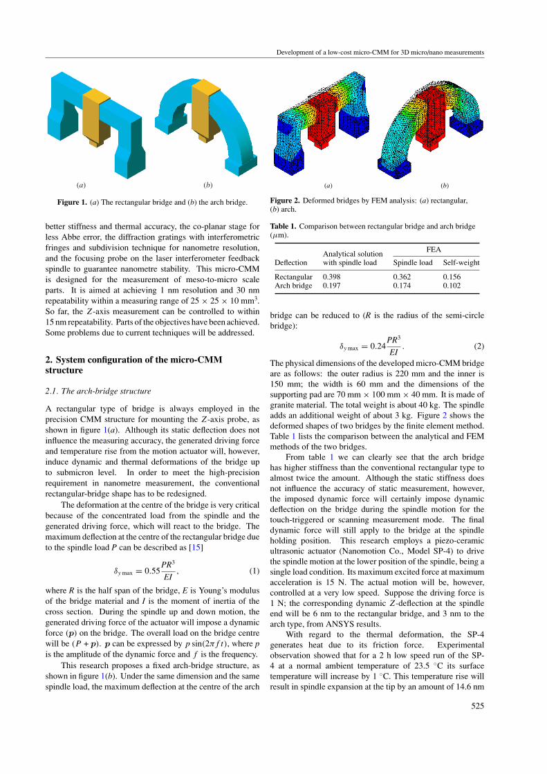
Figure 1. (a) The rectangular bridge and (b) the arch bridge.
better stiffness and thermal accuracy, the co-planar stage forless Abbe error, the diffraction gratings with interferometricfringes and subdivision technique for nanometre resolution,and the focusing probe on the laser interferometer feedbackspindle to guarantee nanometre stability. This micro-CMMis designed for the measurement of meso-to-micro scaleparts. It is aimed at achieving 1 nm resolution and 30 nmrepeatability within a measuring range of 25 × 25 × 10 mm3.So far, the Z-axis measurement can be controlled to within15 nm repeatability. Parts of the objectives have been achieved.Some problems due to current techniques will be addressed.
2. System configuration of the micro-CMMstructure
2.1. The arch-bridge structure
A rectangular type of bridge is always employed in theprecision CMM structure for mounting the Z-axis probe, asshown in figure 1(a). Although its static deflection does notinfluence the measuring accuracy, the generated driving forceand temperature rise from the motion actuator will, however,induce dynamic and thermal deformations of the bridge upto submicron level. In order to meet the high-precisionrequirement in nanometre measurement, the conventionalrectangular-bridge shape has to be redesigned.
The deformation at the centre of the bridge is very criticalbecause of the concentrated load from the spindle and thegenerated driving force, which will react to the bridge. Themaximum deflection at the centre of the rectangular bridge dueto the spindle load P can be described as [15]
δy max = 0.55PR3
EI, (1)
where R is the half span of the bridge, E is Young’s modulusof the bridge material and I is the moment of inertia of thecross section. During the spindle up and down motion, thegenerated driving force of the actuator will impose a dynamicforce (p) on the bridge. The overall load on the bridge centrewill be (P + p). p can be expressed by p sin(2πf t), where pis the amplitude of the dynamic force and f is the frequency.
This research proposes a fixed arch-bridge structure, asshown in figure 1(b). Under the same dimension and the samespindle load, the maximum deflection at the centre of the arch
(a) (b)
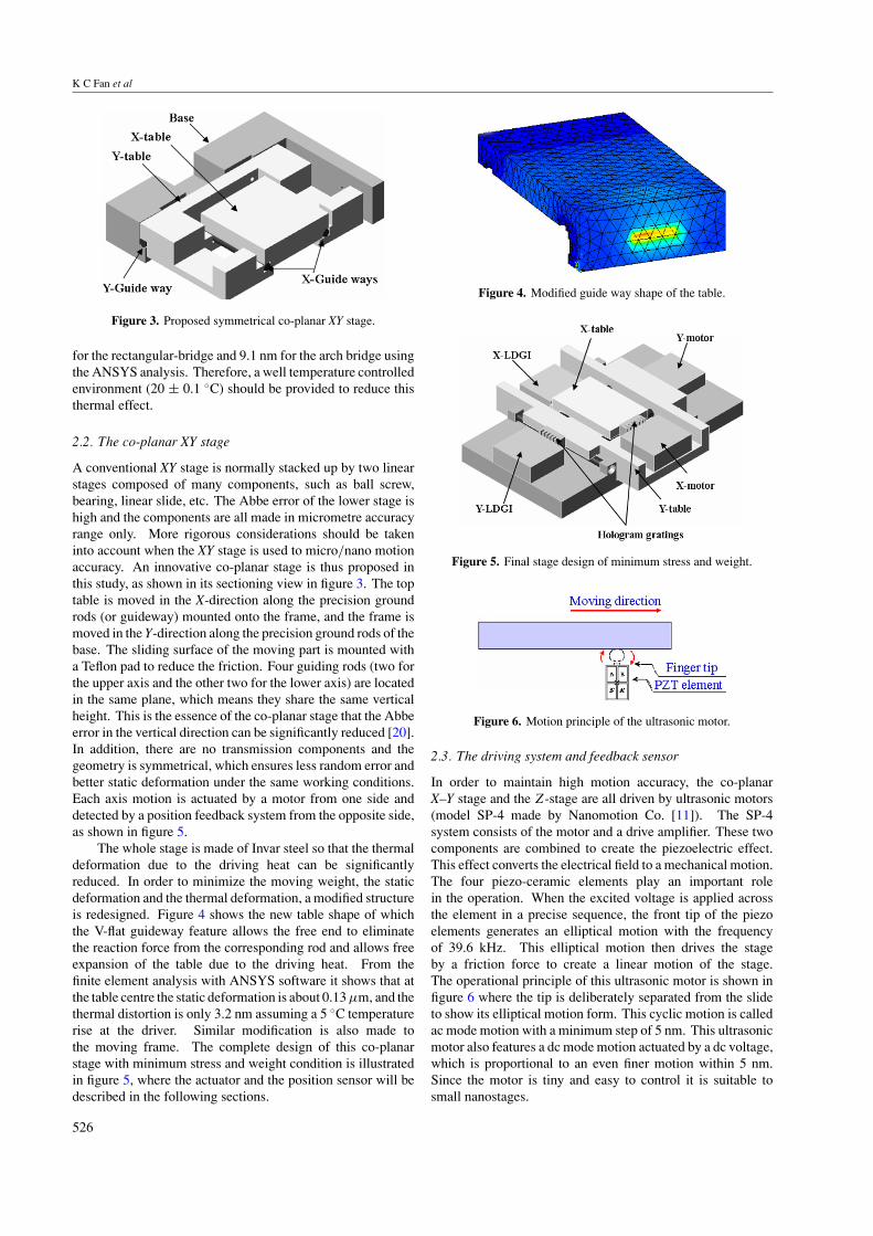
Figure 2. Deformed bridges by FEM analysis: (a) rectangular,(b) arch.
Table 1. Comparison between rectangular bridge and arch bridge(µm).
FEAAnalytical solutionDeflection with spindle load Spindle load Self-weight
Rectangular 0.398 0.362 0.156Arch bridge 0.197 0.174 0.102
bridge can be reduced to (R is the radius of the semi-circlebridge):
δy max = 0.24PR3
EI. (2)
The physical dimensions of the developed micro-CMM bridgeare as follows: the outer radius is 220 mm and the inner is150 mm; the width is 60 mm and the dimensions of thesupporting pad are 70 mm × 100 mm × 40 mm. It is made ofgranite material. The total weight is about 40 kg. The spindleadds an additional weight of about 3 kg. Figure 2 shows thedeformed shapes of two bridges by the finite element method.Table 1 lists the comparison between the analytical and FEMmethods of the two bridges.
From table 1 we can clearly see that the arch bridgehas higher stiffness than the conventional rectangular type toalmost twice the amount. Although the static stiffness doesnot influence the accuracy of static measurement, however,the imposed dynamic force will certainly impose dynamicdeflection on the bridge during the spindle motion for thetouch-triggered or scanning measurement mode. The finaldynamic force will still apply to the bridge at the spindleholding position. This research employs a piezo-ceramicultrasonic actuator (Nanomotion Co., Model SP-4) to drivethe spindle motion at the lower position of the spindle, being asingle load condition. Its maximum excited force at maximumacceleration is 15 N. The actual motion will be, however,controlled at a very low speed. Suppose the driving force is1 N; the corresponding dynamic Z-deflection at the spindleend will be 6 nm to the rectangular bridge, and 3 nm to thearch type, from ANSYS results.
With regard to the thermal deformation, the SP-4generates heat due to its friction force. Experimentalobservation showed that for a 2 h low speed run of the SP-4 at a normal ambient temperature of 23.5 ◦C its surfacetemperature will increase by 1 ◦C. This temperature rise willresult in spindle expansion at the tip by an amount of 14.6 nm
525
K C Fan et al
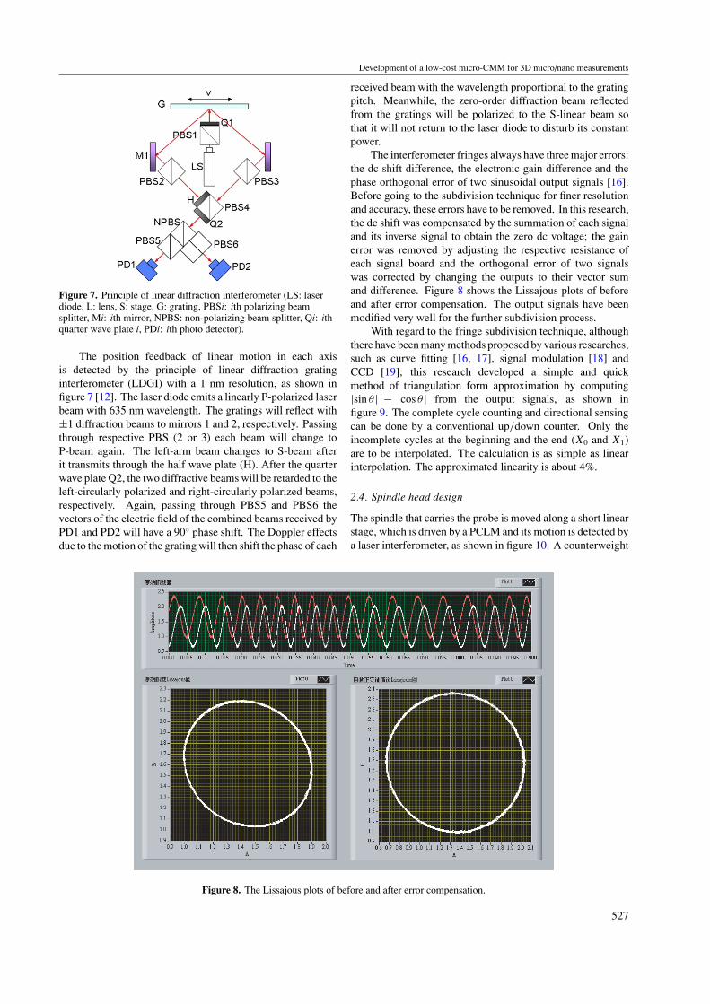
Figure 3. Proposed symmetrical co-planar XY stage.
for the rectangular-bridge and 9.1 nm for the arch bridge usingthe ANSYS analysis. Therefore, a well temperature controlledenvironment (20 ± 0.1 ◦C) should be provided to reduce thisthermal effect.
2.2. The co-planar XY stage
A conventional XY stage is normally stacked up by two linearstages composed of many components, such as ball screw,bearing, linear slide, etc. The Abbe error of the lower stage ishigh and the components are all made in micrometre accuracyrange only. More rigorous considerations should be takeninto account when the XY stage is used to micro/nano motionaccuracy. An innovative co-planar stage is thus proposed inthis study, as shown in its sectioning view in figure 3. The toptable is moved in the X-direction along the precision groundrods (or guideway) mounted onto the frame, and the frame ismoved in the Y-direction along the precision ground rods of thebase. The sliding surface of the moving part is mounted witha Teflon pad to reduce the friction. Four guiding rods (two forthe upper axis and the other two for the lower axis) are locatedin the same plane, which means they share the same verticalheight. This is the essence of the co-planar stage that the Abbeerror in the vertical direction can be significantly reduced [20].In addition, there are no transmission components and thegeometry is symmetrical, which ensures less random error andbetter static deformation under the same working conditions.Each axis motion is actuated by a motor from one side anddetected by a position feedback system from the opposite side,as shown in figure 5.
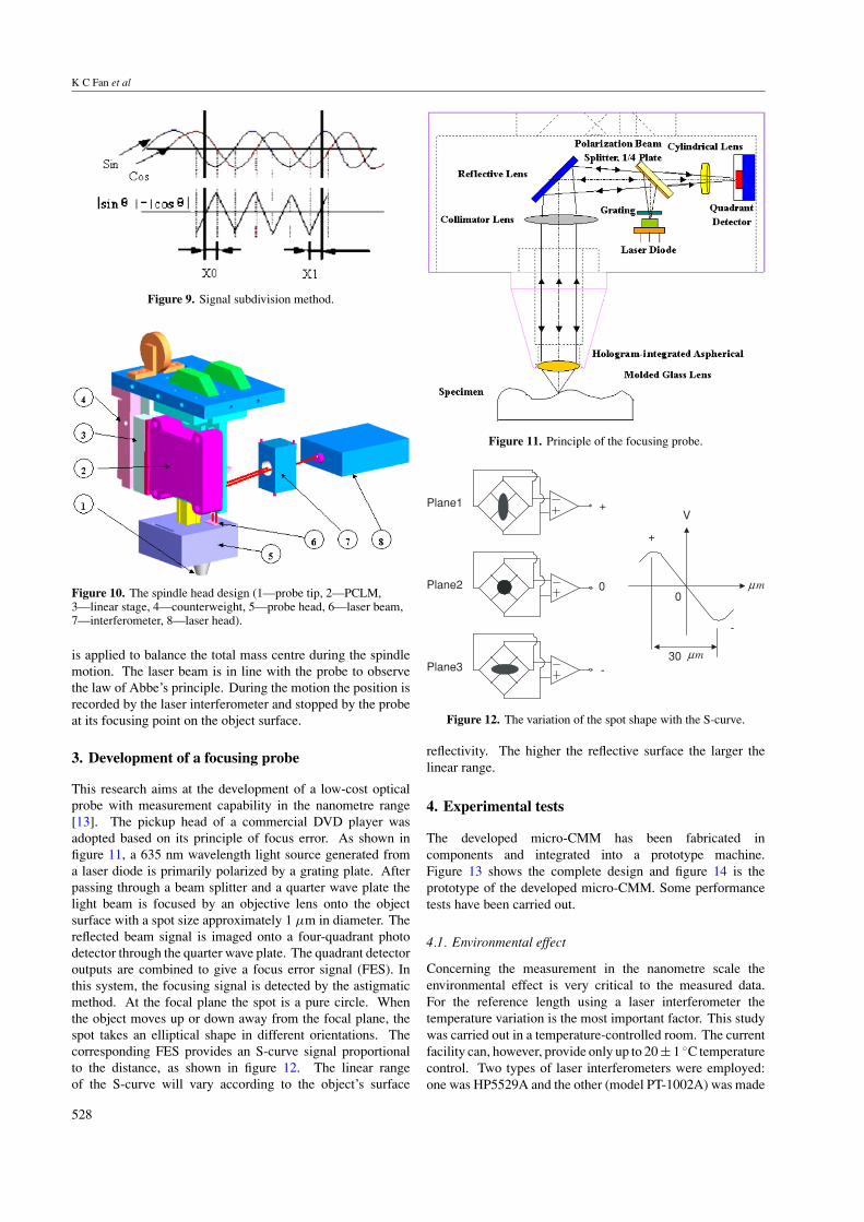
The whole stage is made of Invar steel so that the thermaldeformation due to the driving heat can be significantlyreduced. In order to minimize the moving weight, the staticdeformation and the thermal deformation, a modified structureis redesigned. Figure 4 shows the new table shape of whichthe V-flat guideway feature allows the free end to eliminatethe reaction force from the corresponding rod and allows freeexpansion of the table due to the driving heat. From thefinite element analysis with ANSYS software it shows that atthe table centre the static deformation is about 0.13 µm, and thethermal distortion is only 3.2 nm assuming a 5 ◦C temperaturerise at the driver. Similar modification is also made tothe moving frame. The complete design of this co-planarstage with minimum stress and weight condition is illustratedin figure 5, where the actuator and the position sensor will bedescribed in the following sections.
Figure 4. Modified guide way shape of the table.
Figure 5. Final stage design of minimum stress and weight.
Figure 6. Motion principle of the ultrasonic motor.
2.3. The driving system and feedback sensor
In order to maintain high motion accuracy, the co-planarX–Y stage and the Z-stage are all driven by ultrasonic motors(model SP-4 made by Nanomotion Co. [11]). The SP-4system consists of the motor and a drive amplifier. These twocomponents are combined to create the piezoelectric effect.This effect converts the electrical field to a mechanical motion.The four piezo-ceramic elements play an important rolein the operation. When the excited voltage is applied acrossthe element in a precise sequence, the front tip of the piezoelements generates an elliptical motion with the frequencyof 39.6 kHz. This elliptical motion then drives the stageby a friction force to create a linear motion of the stage.The operational principle of this ultrasonic motor is shown infigure 6 where the tip is deliberately separated from the slideto show its elliptical motion form. This cyclic motion is calledac mode motion with a minimum step of 5 nm. This ultrasonicmotor also features a dc mode motion actuated by a dc voltage,which is proportional to an even finer motion within 5 nm.Since the motor is tiny and easy to control it is suitable tosmall nanostages.
526
Development of a low-cost micro-CMM for 3D micro/nano measurements
Figure 7. Principle of linear diffraction interferometer (LS: laserdiode, L: lens, S: stage, G: grating, PBSi: ith polarizing beamsplitter, Mi: ith mirror, NPBS: non-polarizing beam splitter, Qi: ithquarter wave plate i, PDi: ith photo detector).
The position feedback of linear motion in each axisis detected by the principle of linear diffraction gratinginterferometer (LDGI) with a 1 nm resolution, as shown infigure 7 [12]. The laser diode emits a linearly P-polarized laserbeam with 635 nm wavelength. The gratings will reflect with±1 diffraction beams to mirrors 1 and 2, respectively. Passingthrough respective PBS (2 or 3) each beam will change toP-beam again. The left-arm beam changes to S-beam afterit transmits through the half wave plate (H). After the quarterwave plate Q2, the two diffractive beams will be retarded to theleft-circularly polarized and right-circularly polarized beams,respectively. Again, passing through PBS5 and PBS6 thevectors of the electric field of the combined beams received byPD1 and PD2 will have a 90◦ phase shift. The Doppler effectsdue to the motion of the grating will then shift the phase of each
Figure 8. The Lissajous plots of before and after error compensation.
received beam with the wavelength proportional to the gratingpitch. Meanwhile, the zero-order diffraction beam reflectedfrom the gratings will be polarized to the S-linear beam sothat it will not return to the laser diode to disturb its constantpower.
The interferometer fringes always have three major errors:the dc shift difference, the electronic gain difference and thephase orthogonal error of two sinusoidal output signals [16].Before going to the subdivision technique for finer resolutionand accuracy, these errors have to be removed. In this research,the dc shift was compensated by the summation of each signaland its inverse signal to obtain the zero dc voltage; the gainerror was removed by adjusting the respective resistance ofeach signal board and the orthogonal error of two signalswas corrected by changing the outputs to their vector sumand difference. Figure 8 shows the Lissajous plots of beforeand after error compensation. The output signals have beenmodified very well for the further subdivision process.
With regard to the fringe subdivision technique, althoughthere have been many methods proposed by various researches,such as curve fitting [16, 17], signal modulation [18] andCCD [19], this research developed a simple and quickmethod of triangulation form approximation by computing|sin θ | − |cos θ | from the output signals, as shown infigure 9. The complete cycle counting and directional sensingcan be done by a conventional up/down counter. Only theincomplete cycles at the beginning and the end (X0 and X1)are to be interpolated. The calculation is as simple as linearinterpolation. The approximated linearity is about 4%.
2.4. Spindle head design
The spindle that carries the probe is moved along a short linearstage, which is driven by a PCLM and its motion is detected bya laser interferometer, as shown in figure 10. A counterweight
527
K C Fan et al
Figure 9. Signal subdivision method.
Figure 10. The spindle head design (1—probe tip, 2—PCLM,3—linear stage, 4—counterweight, 5—probe head, 6—laser beam,7—interferometer, 8—laser head).
is applied to balance the total mass centre during the spindlemotion. The laser beam is in line with the probe to observethe law of Abbe’s principle. During the motion the position isrecorded by the laser interferometer and stopped by the probeat its focusing point on the object surface.
3. Development of a focusing probe
This research aims at the development of a low-cost opticalprobe with measurement capability in the nanometre range[13]. The pickup head of a commercial DVD player wasadopted based on its principle of focus error. As shown infigure 11, a 635 nm wavelength light source generated froma laser diode is primarily polarized by a grating plate. Afterpassing through a beam splitter and a quarter wave plate thelight beam is focused by an objective lens onto the objectsurface with a spot size approximately 1 µm in diameter. Thereflected beam signal is imaged onto a four-quadrant photodetector through the quarter wave plate. The quadrant detectoroutputs are combined to give a focus error signal (FES). Inthis system, the focusing signal is detected by the astigmaticmethod. At the focal plane the spot is a pure circle. Whenthe object moves up or down away from the focal plane, thespot takes an elliptical shape in different orientations. Thecorresponding FES provides an S-curve signal proportionalto the distance, as shown in figure 12. The linear rangeof the S-curve will vary according to the object’s surface
Figure 11. Principle of the focusing probe.
Plane1
Plane2
Plane3
V
-
0
+
0
+
-
mµ30
mµ
Figure 12. The variation of the spot shape with the S-curve.
reflectivity. The higher the reflective surface the larger thelinear range.
4. Experimental tests
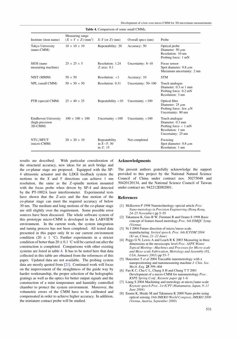
The developed micro-CMM has been fabricated incomponents and integrated into a prototype machine.Figure 13 shows the complete design and figure 14 is theprototype of the developed micro-CMM. Some performancetests have been carried out.
4.1. Environmental effect
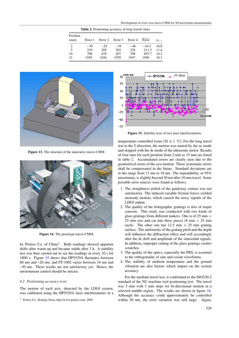
Concerning the measurement in the nanometre scale theenvironmental effect is very critical to the measured data.For the reference length using a laser interferometer thetemperature variation is the most important factor. This studywas carried out in a temperature-controlled room. The currentfacility can, however, provide only up to 20 ± 1 ◦C temperaturecontrol. Two types of laser interferometers were employed:one was HP5529A and the other (model PT-1002A) was made
528
Development of a low-cost micro-CMM for 3D micro/nano measurements
Table 2. Positioning accuracy of long travels (nm).
Position(mm) Error 1 Error 2 Error 3 Error 4 Error σn−1
2 −49 −29 −54 −46 −44.5 10.85 210 205 203 228 211.5 11.4
10 708 678 697 708 697.7 14.215 1955 1926 1970 1947 1950 18.3
Figure 13. The structure of the innovative micro-CMM.
Figure 14. The prototype micro-CMM.
by Pretios Co. of China3. Both readings showed apparentdrifts after warm-up and became stable after 3 h. A stabilitytest was then carried out to see the readings at every 10 s for1800 s. Figure 15 shows that HP5529A fluctuates between60 nm and –20 nm, and PT-1002 varies between 18 nm and–30 nm. These results are not satisfactory yet. Hence, theenvironment control should be stricter.
4.2. Positioning accuracy tests
The motion of each axis, detected by the LDGI system,was calibrated using the HP5529A laser interferometer in a
3 Pretios Co., Beijing China, http://www.pretios.com, 2005.
Figure 15. Stability tests of two laser interferometers.
temperature-controlled room (20 ± 1 ◦C). For the long traveltest in the Y-direction, the motion was started by the ac modeand stopped with the dc mode of the ultrasonic motor. Resultsof four runs for each position from 2 mm to 15 mm are listedin table 2. Accumulated errors are clearly seen due to thegeometrical errors of the axis motion. These systematic errorsshall be compensated in the future. Standard deviations arein the range from 11 nm to 18 nm. The repeatability, or 95%uncertainty, is slightly beyond 30 nm after 10 mm travel. Somepossible error sources were found as follows.
1. The straightness polish of the guideway contact was notsatisfactory. The induced variable friction forces yieldedunsteady motion, which caused the noisy signals of theLDGI output.
2. The quality of the holographic gratings is also of majorconcern. This study was conducted with two kinds ofglass gratings from different makers. One is of 25 mm ×25 mm size and cut into three pieces (8 mm × 25 mmeach). The other one has 12.5 mm × 25 mm gratingsurface. The uniformity of the grating pitch and the depthwill influence the diffraction effect and will accordinglyalter the dc drift and amplitude of the sinusoidal signals.In addition, improper cutting of the glass gratings createsscratches.
3. The quality of the optics, especially the PBS, is essentialto the orthogonality of sine and cosine waveforms.
4. The stability of ambient temperature and the groundvibration are also factors which impact on the systemaccuracy.
For the medium travel test, it conformed to the ISO230-2standard of the NC machine tool positioning test. The travelwas 5 mm with 1 mm steps for bi-directional motion in aselected middle region. The results are shown in figure 16.Although the accuracy could approximately be controlledwithin 30 nm, the error variation was still large. Again,
529
K C Fan et al
Table 3. Positioning accuracy of fine motions (nm).
Position(mm) Error 1 Error 2 Error 3 Error 4 Error σn−1
0 0 0 0 0 0 00.1 −5 −13 −17 −10 −11.2 5.10.2 −19 −32 −27 −28 −26.5 5.50.3 −27 −8 −26 −33 −23.5 10.80.4 −34 −33 −33 −26 −31.5 3.70.5 −11 −14 −20 −13 −14.5 3.90.6 0 −11 −20 21 −2.5 17.70.7 17 2 −16 4 1.7 13.60.8 27 4 3 32 16.5 15.10.9 14 15 5 23 14.3 7.41 7 29 19 4 14.8 11.5
-60
-40
-20
0
20
40
60
0 1 2 3 4 5
Displacement (mm)
Err
or (
nm)
Forward avg
Backward avg
Figure 16. Medium travel positioning accuracy of one axis.
the temperature effect could be the major source, which notonly varies the LDGI readings but also those of the laserinterferometer.
For the fine motion test of 1 mm travel with 100 µm stepsfor four runs, the averaged error could possibly fall into the30 nm range with only one exception, as shown in table 3.Since the tested position was specially selected, the errorsources of long travels did not exist because there was nomissing pitch count of the gratings. However, althoughthe duration of this test was short, the variation of the HPlaser interferometer readings could not be eliminated. Thetemperature variation might dominate the errors.
4.3. Focus probe test
The focus error signal (FES) test was carried out by mountingthe probe on a linear stage. The stage motion was measured bya laser interferometer. Figure 17 shows the tested results withrespect to different materials. A good S-curve occurs whenthe material has a good reflective surface [14].
4.4. Spindle motion tests
A small piece of mirror was mounted onto the table top ofthe co-planar stage as an object. Initially, the spindle was
S-Curve vs. Material
-3000
-2000
-1000
0
1000
2000
3000
20 30 40 50 60 70 80
Position (µm)
FE
S (
mV
)
Figure 17. S-curves for various materials.
Figure 18. Repeatability test of spindle and probe system.
moved to focus the probe beam right on the mirror surface sothat the FES output was zero voltage. The spindle was thenmoved away a random distance each time and returned untilthe FES was zero again. The PT-1002A laser interferometerwas mounted to detect the spindle motion. The approachingspeed for the focus point detection should be very slow in orderto avoid any induced dynamic errors. In practice, from a fardistance (several millimetres) the approaching speed was about1 mm s−1; within 100 µm the speed was reduced to20 µm s−1; within 100 nm the dc mode of the ultrasonicmotor was used with about 10 nm per step. The readings ofthe laser interferometer at each focus position showed quitea good repeatability within 15 nm for 12 runs, as shown infigure 18. As indicated in figure 15, PT-1002A has smallerfluctuation with the time span; the spindle motion is quitesuccessful and reliable.
5. Concluding remarks
This paper states the current progress of the developmentof a micro-CMM. Design considerations and preliminary
530
Development of a low-cost micro-CMM for 3D micro/nano measurements
Table 4. Comparison of some small CMMs.
Measuring rangeInstitute (item name) (X × Y × Z) (mm3) X–Y (or Z) (nm) Overall specs (nm) Probe
Tokyo University 10 × 10 × 10 Repeatability: 20 Accuracy: 50 Optical probe(nano-CMM) Diameter: 50 µm
Resolution: 10 nmProbing force: 1 mN
SIOS (nano 25 × 25 × 5 Resolution: 1.24 Uncertainty: 8–10 Focus sensormeasuring machine) Z-axis: 0.1 Spot diameter: 0.8 µm
Maximum uncertainty: 2 nm
NIST (MMM) 50 × 50 Resolution: <1 Accuracy: 10 STM
NPL (small CMM) 50 × 50 × 50 Resolution: 0.31 Uncertainty: 50–100 Touch analogueDiameter: 0.3 or 1 mmProbing force: 0.2 mNResolution: 3 nm
PTB (special CMM) 25 × 40 × 25 Repeatability <10 Uncertainty <100 Optical fibreDiameter: 25 µmProbing force: few µNUncertainty: 80 nm
Eindhoven University 100 × 100 × 100 Uncertainty <100 Uncertainty <100 Touch analogue(high-precision Diameter: 0.3 mm3D-CMM) Probing force < 1 mN
Resolution: 1 nmUncertainty: 25 nm
NTU/HFUT 20 × 20 × 10 Repeatability Not completed Focusing(micro-CMM) in X−Y: 30 Spot diameter: 0.8 µm
in Z: 15 Resolution: 1 nm
results are described. With particular consideration ofthe structural accuracy, new ideas for an arch bridge andthe co-planar stage are proposed. Equipped with the SP-4 ultrasonic actuator and the LDGI feedback system themotions in the X and Y directions can achieve 1 nmresolution, the same as the Z-spindle motion mountedwith the focus probe when driven by SP-4 and detectedby the PT-1002A laser interferometer. Experimental testshave shown that the Z-axis and the fine motion of theco-planar stage can meet the required accuracy of below30 nm. The medium and long motions of the co-planar stageare still slightly over the requirement. Some possible errorsources have been discussed. The whole software system ofthis prototype micro-CMM is developed in the LABVIEWenvironment. In the current work, the system integrationand tuning process has not been completed. All tested datapresented in this paper only fit to our current environmentcondition (20 ± 1 ◦C). Further experiments in a strictercondition of better than 20 ± 0.1 ◦C will be carried out after theconstruction is completed. Comparisons with other existingsystems are listed in table 4. It has to be noted here that datacollected in this table are obtained from the references of thispaper. Updated data are not available. The probing systemdata are mostly quoted from [21]. Continued work will focuson the improvement of the straightness of the guide way byharder workmanship, the proper selection of the holographicgratings as well as the optics for better output signals and theconstruction of a mini temperature and humidity controlledchamber to protect the system environment. Moreover, thevolumetric errors of the CMM have to be calibrated andcompensated in order to achieve higher accuracy. In addition,the miniature contact probe will be studied.
Acknowledgments
The present authors gratefully acknowledge the supportprovided to this project by the National Natural ScienceCouncil of China under contract nos. 50275048 and50420120134, and the National Science Council of Taiwanunder contract no. 942212E002001.
References
[1] McKeown P 1998 Nanotechnology–special article Proc.Nano-metrology in Precision Engineering (Hong Kong,24–25 November) pp 5–55
[2] Takamasu K, Guo B W, Furutani R and Ozano S 1998 Basicconcept of feature-based metrology Proc. 6th ISMQC Symp.(Vienna)
[3] Ni J 2004 Future direction of micro/meso-scalemanufacturing Invited speech, Proc. 6th ICFDM’2004(Xi’an, China, 21–23 June)
[4] Peggs G N, Lewis A and Leach R K 2003 Measuring in threedimensions at the mesoscopic level Proc. ASPE WinterTopical Meeting—Machines and Processes for Micro-scaleand Meso-scale Fabrication, Metrology and Assembly (FL,USA, January 2003) pp 53–7
[5] Hausottee T et al 2004 Traceable nanometrology with ananopositioning and nanomeasuring machine J. Chin. Soc.Mech. Eng. 25 399–404
[6] Fan K C, Chu C L, Chang S H and Chung T T 2001Development of a micro-CMM for nanometrology Proc.KSPE Spring Conf., Keynote paper pp 1–6
[7] Liang S 2004 Machining and metrology at micro/nano scaleKeynote speech Proc. 1st ICPT (Hamamatsu, Japan, 9–11June 2004)
[8] Enami K, Hiraki M and Takamasu K 2000 Nano probe usingoptical sensing 16th IMEKO World Congress, IMEKO 2000(Vienna, Austria, September 2000)
531

K C Fan et al
[9] Haitjema H, Pril W O and Schellekens P 2001 Development ofa silicon-based nanoprobe system for 3-D measurementsAnn. CIRP 50 365–8
[10] Schwenke H, Hartig F, Wendit K and Waldele F 2001Future challenges in co-ordinate metrology:addressing metrological problems for very smalland very large parts IDW Conf. (Knoxville, TN)pp 1–12
[11] Pohl D W 1987 Dynamic piezoelectric translation devices Rev.Sci. Instrum. 58 54–7
[12] Fan K C 2002 A high precision diffraction interferometrystylus probing system Keynote paper Proc. ICMT(Kitakyushu, Japan)
[13] Fan K C, Chu C L and Mou J I 2001 Development of alow-cost autofocusing probe for profile measurement Meas.Sci. Technol. 12 2137–46
[14] Fan K C, Lin C Y and Shyu L H 2000 Development of alow-cost focusing probe for profile measurement Meas. Sci.Technol. 11 1–7
[15] Fan K C, Wang W L and Chen F 2004 Innovative design of anew CMM bridge Proc. ISPMM 2004 (Beijing, China,August 2004) paper no 50
[16] Heydemann P L M 1981 Determination and correction ofquadrature correction of fringe measurement errors ininterferometers Appl. Opt. 20 3382
[17] Birch K P 1990 Optical fringe subdivision with nanometricaccuracy Precis. Eng. 12 195–8
[18] Chen B Y and Li D C 2002 Progress in studies on long-rangeand ultrahigh-accuracy nanometer measurements Proc. 2ndISIST (Jinan, China) vol 2 pp 84–9
[19] Wen P and Hsu D H 1990 Direct subdivision of moire fringewith CCD Proc. SPIE 1230 165–6
[20] Burton G L and Burton P J 1996 X–Y–Theta positioningmechanism US Patent No. 5523942
[21] Weckenmann A, Peggs G and Hoffmann J 2005 Probingsystems for dimensional micro and nano metrology Proc.ISMTII 2005 (Huddersfield, UK, September 2005)pp 199–206
532