Embed Size (px)
Citation preview
M102506_XC4VFX60
Synopsis V2.0 Heavy ion SEL test of Virtex4 FPGA XC4VFX60 from Xilinx
Christian Poivey1, Melanie Berg1, Scott Stansberry2, Mark Friendlich1, Hak Kim1,
Dave Petrick3, Jim Howard1, Ray Ladbury3, Ken LaBel3
1Muniz Engineering Inc. 2University of Southern California
3NASA-GSFC
Test Date(s): October 26-28, 2006 Report Date: February 1, 2007
I. Introduction
This study has been undertaken to determine the single event destructive susceptibility of the Xilinx Virtex 4 Field Programmable Gate Array (FPGA) XC4VFX60. Device under test (DUT) was monitored for destructive events induced by exposing it to a heavy ion beam at the Michigan State Cyclotron Single Event Effects Test Facility. Test was performed in the frame of HST/RNS and ELC projects.
II. Devices Tested
Device part number is XC4VFX60-10FF1152CES1. XC4VFX60 FPGA features are: - 56880 logic cells - 232 Kbits of block RAM/FIFO with ECC - 4176 Kbits of block RAM - 12 Digital Clock Manager (DCM) - 8 phase matched clock dividers (PMCD) - 288 max differential I/O pairs - 128 Xtreme DSP slices - 2 Power PC405 processors blocks - 4 Ethernet MAC blocks - 16 Rocket I/O Multi gigabit transceivers (MGT) - 22,262,016 configuration memory bits - 576 max select I/O
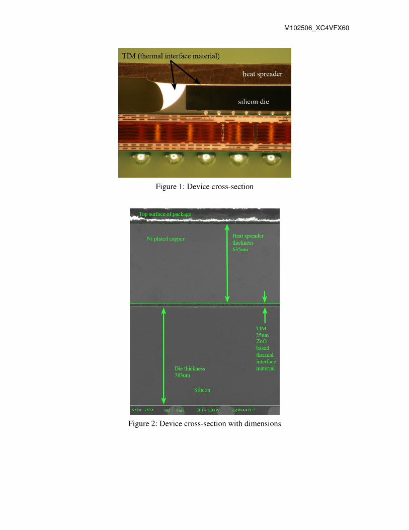
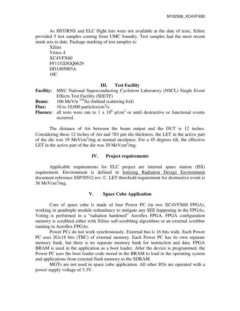
Device technology is 90 nm Copper CMOS. Device is packaged in a 1152 pin flip-chip fine pitch BGA package. Max package thickness is 2.8mm. Lid thickness is 0.65 +/- 0.05 mm. Lid material is C1100 or CDA194 (97.42% Cu, 2.4% I, 0.1% Zn, Ph 0.05% Ph). Die thickness is between 0.725 and 0.775 mm. Device cross-sections are shown in Figures 1 and 2. Device was irradiated without lid.
Four test samples mounted in daughter board were available for the test.
M102506_XC4VFX60
Figure 1: Device cross-section
Figure 2: Device cross-section with dimensions
M102506_XC4VFX60
As HST/RNS and ELC flight lots were not available at the date of tests, Xilinx provided 5 test samples coming from UMC foundry. Test samples had the most recent mask sets to date. Package marking of test samples is:
Xilinx Virtex-4 XC4VFX60 FF1152DGQ0629 DD1405003A 10C
III. Test Facility
Facility: MSU National Superconducting Cyclotron Laboratory (NSCL) Single Event Effects Test Facility (SEETF)
Beam: 106 MeV/u 136Xe (behind scattering foil) Flux: 10 to 10,000 particles/cm2/s. Fluence: all tests were run to 1 x 10⁶ p/cm2 or until destructive or functional events
occurred.
The distance of Air between the beam output and the DUT is 12 inches. Considering these 12 inches of Air and 783 µm die thickness, the LET in the active part of the die was 19 MeVcm2/mg at normal incidence. For a 45 degrees tilt, the effective LET in the active part of the die was 30 MeVcm2/mg.
IV. Project requirements Applicable requirements for ELC project are internal space station (ISS)
requirement. Environment is defined in Ionizing Radiation Design Environment document reference SSP30512 rev. C. LET threshold requirement for destructive event is 36 MeVcm2/mg.
V. Space Cube Application Core of space cube is made of four Power PC (in two XC4VFX60 FPGA),
working in quadruple module redundancy to mitigate any SEE happening in the FPGAs. Voting is performed in a “radiation hardened” Aeroflex FPGA. FPGA configuration memory is scrubbed either with Xilinx self-scrubbing algorithms or an external scrubber running in Aeroflex FPGAs.
Power PCs do not work synchronously. External bus is 16 bits wide. Each Power PC uses 2Gx18 bits (TBC) of external memory. Each Power PC has its own separate memory bank, but there is no separate memory bank for instruction and data. FPGA BRAM is used in the application as a boot loader. After the device is programmed, the Power PC uses the boot loader code stored in the BRAM to load in the operating system and applications from external flash memory to the SDRAM.
MGTs are not used in space cube application. All other I/Os are operated with a power supply voltage of 3.3V.
M102506_XC4VFX60
No PMCDs are currently used in the application, but multiple MCD are used. Power PC clock speed is 250 MHz (to be increased to 350 or 375 MHz for flight). Clock speed for I/Os is 125 MHz.
VI. Test Conditions and Error Modes
Test Temperature: 25˚C and 80˚C (die)* Operating Frequency: 250 MHz for Power PC, 125 MHz for I/Os Power Supply Voltage: Vccint: 1.26V Vccaux: 2.62V
Vcco: 3.45V
* maximum junction temperature is 125˚C. Die temperature is given by DUT internal temperature sensing diode.
PARAMETERS OF INTEREST: Power supply currents, device functionality SEE Conditions: SEL, SEU, MEU, SET, SEFI (for this test we have only looked
at SEL or other destructive condition and SEFI)
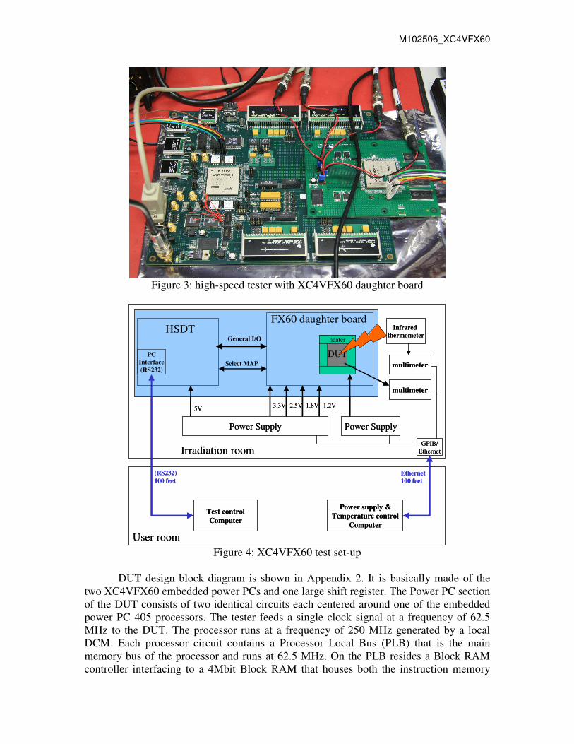
VII. Test Set-up XC4VFX60 was tested with NASA-GSFC REAG (Radiation Effects and
Analysis Group) high-speed digital tester (HSDT). HSDT is a reusable universal digital device tester based on Xilinx Virtex 2 Pro FPGA with input/output (I/O) operation speed up to 600 MHz.
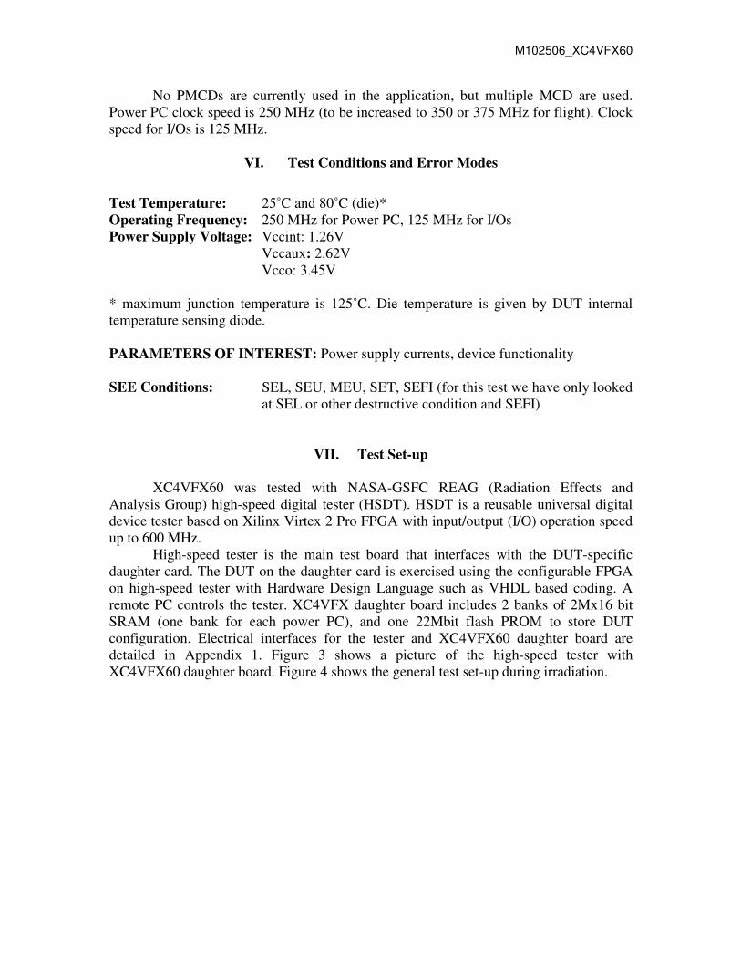
High-speed tester is the main test board that interfaces with the DUT-specific daughter card. The DUT on the daughter card is exercised using the configurable FPGA on high-speed tester with Hardware Design Language such as VHDL based coding. A remote PC controls the tester. XC4VFX daughter board includes 2 banks of 2Mx16 bit SRAM (one bank for each power PC), and one 22Mbit flash PROM to store DUT configuration. Electrical interfaces for the tester and XC4VFX60 daughter board are detailed in Appendix 1. Figure 3 shows a picture of the high-speed tester with XC4VFX60 daughter board. Figure 4 shows the general test set-up during irradiation.
M102506_XC4VFX60
Figure 3: high-speed tester with XC4VFX60 daughter board
Irradiation room
HSDTFX60 daughter board
General I/O
Select MAPDUTPC
Interface(RS232)
Power Supply Power Supply
3.3V 2.5V 1.8V 1.2V5V
heater
Infrared thermometer
multimeter
multimeter
GPIB/Ethernet
User room
Test controlComputer
Power supply &Temperature control
Computer
(RS232)100 feet
Ethernet100 feet
Figure 4: XC4VFX60 test set-up
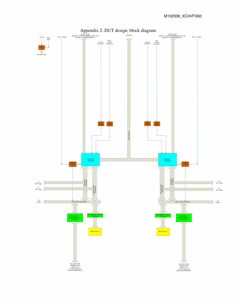
DUT design block diagram is shown in Appendix 2. It is basically made of the
two XC4VFX60 embedded power PCs and one large shift register. The Power PC section of the DUT consists of two identical circuits each centered around one of the embedded power PC 405 processors. The tester feeds a single clock signal at a frequency of 62.5 MHz to the DUT. The processor runs at a frequency of 250 MHz generated by a local DCM. Each processor circuit contains a Processor Local Bus (PLB) that is the main memory bus of the processor and runs at 62.5 MHz. On the PLB resides a Block RAM controller interfacing to a 4Mbit Block RAM that houses both the instruction memory
M102506_XC4VFX60
and data memory for all operations of the power PC. Each Power PC uses 64Kbytes of BRAM. (15554 bytes are effectively used for PPC code and data). Each processor communicates to the tester board through a UART that is attached to an On chip Peripheral Bus (OPB) connected to the PLB by a PLB to OPB bridge. DUT design uses 45 I/Os.
The program running on each DUT (in the BRAM, external SRAM in DUT board was not used for this test) simply waits for a critical or non-critical interrupt. Then, when the interrupt is received, a counter is incremented corresponding to the types of interrupt that is received and a message in ASCII format is sent out through the UART to HSDT board. The format of these messages is a follows:
On startup, PowerPC #0 will send the following message: "\n\r***** PPC 0: Custom Radiation Test Application *****\r\n\n" On startup, PowerPC #1 will send the following message: "\n\r***** PPC 1: Custom Radiation Test Application *****\r\n\n" When an Interrupt is received a message of the following format will be transmitted: "X I MMMM\n\r" where X = Processor # (0 for PPC0, 1 for PPC1) I = Interrupt type (0 for non-critical, 1 for critical) MMMM = the number of interrupts of that type received by that processor
example:"0 1 00C4\n\r" means that PPC0 has received a critical interrupt and it was the 196th (xC4) critical interrupt that it received
Separately from the power PC circuits, 8 x 2000 flip-flop shift registers are implemented. Each shift register runs at 125 Mhz with a 4-bit parallel output operating at 31.25 Mhz representing the next 4 bits of the shift register. These shift registers are presented to the tester board as a 32-bit word with an associated 31.25 Mhz shift_clock.
Total design gate count is 4,400,238. About 10,000 slices are used. During irradiation, DUT power supply currents (Vccint (1.2V), Vccaux(2.5V),
and Vcco(3.3V)) were monitored. Nominal DUT power supply currents are 440 mA, 70 mA, and 95 mA for Vccint, Vccaux, and Vcc0 respectively. As soon as one of the current reaches a programmable SEL detection level (750 mA for core, 500 mA for aux, and 500mA for I/O), the DUT power supplies were shutdown and irradiation was stopped.
One Minco heater mounted on top of DUT die was used to heat the device. DUT
external temperature was monitored with an infrared thermometer. DUT die temperature was measured via the DUT internal temperature sensing diode. Power supply and temperature monitoring and control are performed with a Labview program running on a laptop.
M102506_XC4VFX60
Another Labview program running on another laptop interfaced with HSDT. It set test modes and collects telemetry. HSDT program performed two tasks during the irradiation. Shift register was exercised but not tested:
- Scrub of DUT configuration memory: all configuration memory but BRAM is scrubbed at a frequency of 30 MHz (TBC), scrubbing command is a manual command from Labview program. Test can be run with and without scrubbing.
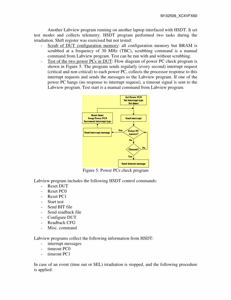
- Test of the two power PCs in DUT: Flow diagram of power PC check program is shown in Figure 5. The program sends regularly (every second) interrupt request (critical and non critical) to each power PC, collects the processor response to this interrupt requests and sends the messages to the Labview program. If one of the power PC hangs (no response to interrupt request), a timeout signal is sent to the Labview program. Test start is a manual command from Labview program.
Set Power PC#
Set interrupt typeSet timer
Send interrupt
Power PCAnswer?Send interrupt message
Reset timerSwap Power PC#
Increment interrupt type
Timeout?
Send timeout message
Yes
No
No
Yes
Set Power PC#Set interrupt type
Set timer
Send interrupt
Power PCAnswer?Send interrupt message
Reset timerSwap Power PC#
Increment interrupt type
Timeout?
Send timeout message
Yes
No
No
Yes
Figure 5: Power PCs check program
Labview program includes the following HSDT control commands:
- Reset DUT - Reset PC0 - Reset PC1 - Start test - Send BIT file - Send readback file - Configure DUT - Readback CFG - Misc. command
Labview programs collect the following information from HSDT:
- interrupt messages - timeout PC0 - timeout PC1
In case of an event (time out or SEL) irradiation is stopped, and the following procedure is applied:
M102506_XC4VFX60
- reset PPC and restart PPC (manual Labview commands) If DUT is up and running again, another irradiation run can be started. If it does not work:
- Reset DUT and restart DUT (manual Labview commands) If DUT is up and running again, another irradiation run can be started. If it does not work:
- Unconfigure and reconfigure DUT (manual Labview commands) If DUT is up and running again, another irradiation run can be started. If it does not work:
- Power cycle DUT and reconfigure If DUT is up and running again, another irradiation run can be started. If it does not work:
- Resend config file to the tester (upset in SRAM storing configuration file?) If DUT is up and running again, another irradiation run can be started. If it does not work:
- Power cycle tester board If DUT is up and running again, another irradiation run can be started List of test equipment is presented in Appendix 3.
VIII. Test Results
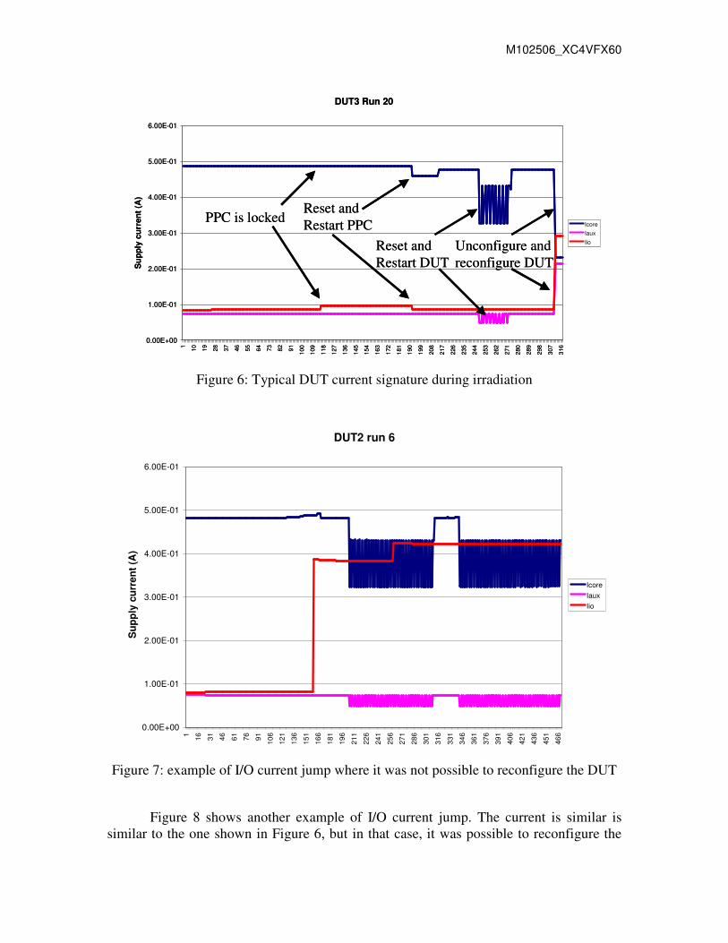
Detailed test results are shown in Appendix 4. No SEL was observed during the experiments, but we saw high current jumps on 3.3V power supply that provides DUT I/O power supply and DUT daughter board SRAMs. During such events, I/O power supply jumps from the nominal value of 95 mA to about 300 mA. I/O power supply current returns to a nominal value after a power cycle. After run6 and a high current jump, DUT#2 was no longer functional even after a power cycle. However, the part was tested again one week after the tests, and it was functional again. For all the other occurrences of high I/O current jump, the part recovered functionality after a power cycle. Figure 6 shows a typical current signature when no I/O jump occurs. Figure 7 shows one case of I/O jump current on DUT #2. It was not possible to reconfigure the DUT in this case.
M102506_XC4VFX60
DUT3 Run 20
0.00E+00
1.00E-01
2.00E-01
3.00E-01
4.00E-01
5.00E-01
6.00E-01
1 10 19 28 37 46 55 64 73 82 91 100
109
118
127
136
145
154
163
172
181
190
199
208
217
226
235
244
253
262
271
280
289
298
307
316
Sup
ply
curr
ent (
A)
IcoreIauxIio
PPC is lockedReset andRestart PPC
Reset andRestart DUT
Unconfigure andreconfigure DUT
Figure 6: Typical DUT current signature during irradiation
DUT2 run 6
0.00E+00
1.00E-01
2.00E-01
3.00E-01
4.00E-01
5.00E-01
6.00E-01
1 16 31 46 61 76 91 106
121
136
151
166
181
196
211
226
241
256
271
286
301
316
331
346
361
376
391
406
421
436
451
466
Sup
ply
curr
ent (
A)
IcoreIauxIio
Figure 7: example of I/O current jump where it was not possible to reconfigure the DUT
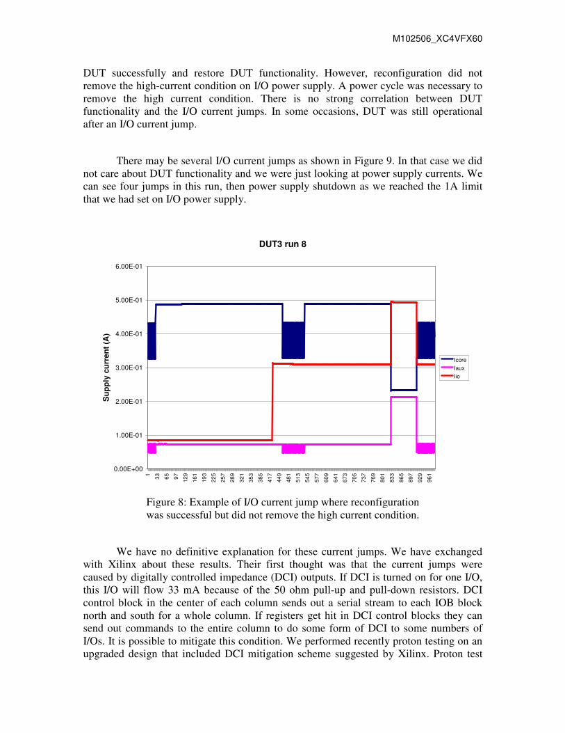
Figure 8 shows another example of I/O current jump. The current is similar is similar to the one shown in Figure 6, but in that case, it was possible to reconfigure the
M102506_XC4VFX60
DUT successfully and restore DUT functionality. However, reconfiguration did not remove the high-current condition on I/O power supply. A power cycle was necessary to remove the high current condition. There is no strong correlation between DUT functionality and the I/O current jumps. In some occasions, DUT was still operational after an I/O current jump.
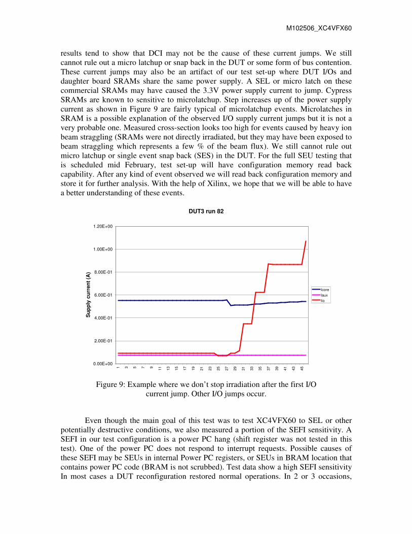
There may be several I/O current jumps as shown in Figure 9. In that case we did not care about DUT functionality and we were just looking at power supply currents. We can see four jumps in this run, then power supply shutdown as we reached the 1A limit that we had set on I/O power supply.
DUT3 run 8
0.00E+00
1.00E-01
2.00E-01
3.00E-01
4.00E-01
5.00E-01
6.00E-01
1 33 65 97 129
161
193
225
257
289
321
353
385
417
449
481
513
545
577
609
641
673
705
737
769
801
833
865
897
929
961
Sup
ply
curr
ent (
A)
IcoreIauxIio
Figure 8: Example of I/O current jump where reconfiguration was successful but did not remove the high current condition.
We have no definitive explanation for these current jumps. We have exchanged with Xilinx about these results. Their first thought was that the current jumps were caused by digitally controlled impedance (DCI) outputs. If DCI is turned on for one I/O, this I/O will flow 33 mA because of the 50 ohm pull-up and pull-down resistors. DCI control block in the center of each column sends out a serial stream to each IOB block north and south for a whole column. If registers get hit in DCI control blocks they can send out commands to the entire column to do some form of DCI to some numbers of I/Os. It is possible to mitigate this condition. We performed recently proton testing on an upgraded design that included DCI mitigation scheme suggested by Xilinx. Proton test
M102506_XC4VFX60
results tend to show that DCI may not be the cause of these current jumps. We still cannot rule out a micro latchup or snap back in the DUT or some form of bus contention. These current jumps may also be an artifact of our test set-up where DUT I/Os and daughter board SRAMs share the same power supply. A SEL or micro latch on these commercial SRAMs may have caused the 3.3V power supply current to jump. Cypress SRAMs are known to sensitive to microlatchup. Step increases up of the power supply current as shown in Figure 9 are fairly typical of microlatchup events. Microlatches in SRAM is a possible explanation of the observed I/O supply current jumps but it is not a very probable one. Measured cross-section looks too high for events caused by heavy ion beam straggling (SRAMs were not directly irradiated, but they may have been exposed to beam straggling which represents a few % of the beam flux). We still cannot rule out micro latchup or single event snap back (SES) in the DUT. For the full SEU testing that is scheduled mid February, test set-up will have configuration memory read back capability. After any kind of event observed we will read back configuration memory and store it for further analysis. With the help of Xilinx, we hope that we will be able to have a better understanding of these events.
DUT3 run 82
0.00E+00
2.00E-01
4.00E-01
6.00E-01
8.00E-01
1.00E+00
1.20E+00
1 3 5 7 9 11 13 15 17 19 21 23 25 27 29 31 33 35 37 39 41 43 45
Sup
ply
curr
ent (
A)
IcoreIauxIio
Figure 9: Example where we don’t stop irradiation after the first I/O
current jump. Other I/O jumps occur.
Even though the main goal of this test was to test XC4VFX60 to SEL or other potentially destructive conditions, we also measured a portion of the SEFI sensitivity. A SEFI in our test configuration is a power PC hang (shift register was not tested in this test). One of the power PC does not respond to interrupt requests. Possible causes of these SEFI may be SEUs in internal Power PC registers, or SEUs in BRAM location that contains power PC code (BRAM is not scrubbed). Test data show a high SEFI sensitivity In most cases a DUT reconfiguration restored normal operations. In 2 or 3 occasions,
M102506_XC4VFX60
reconfigurations did not work. We suspect a neutron hit in the tester board SRAM that stored DUT configuration. Normal operations were restored after resending the BIT file.
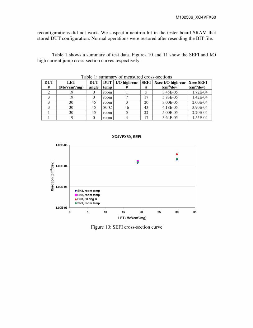
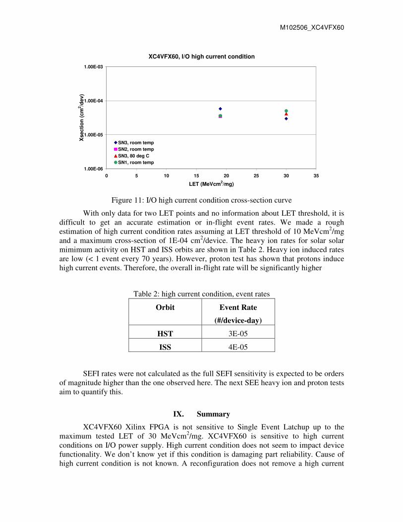
Table 1 shows a summary of test data. Figures 10 and 11 show the SEFI and I/O high current jump cross-section curves respectively.
Table 1: summary of measured cross-sections DUT
# LET
(MeVcm2/mg) DUT angle
DUT temp
I/O high-cur #
SEFI #
Xsec I/O high-cur (cm2/dev)
Xsec SEFI (cm2/dev)
2 19 0 room 1 5 3.45E-05 1.72E-04 3 19 0 room 7 17 5.83E-05 1.42E-04 3 30 45 room 3 20 3.00E-05 2.00E-04 3 30 45 80°C 46 43 4.18E-05 3.90E-04 1 30 45 room 5 22 5.00E-05 2.20E-04 1 19 0 room 4 17 3.64E-05 1.55E-04
XC4VFX60, SEFI
1.00E-06
1.00E-05
1.00E-04
1.00E-03
0 5 10 15 20 25 30 35
LET (MeVcm2/mg)
Xse
ctio
n (c
m2 /d
ev)
SN3, room tempSN2, room tempSN3, 80 deg CSN1, room temp
Figure 10: SEFI cross-section curve
M102506_XC4VFX60
XC4VFX60, I/O high current condition
1.00E-06
1.00E-05
1.00E-04
1.00E-03
0 5 10 15 20 25 30 35
LET (MeVcm2/mg)
Xse
ctio
n (c
m2 /d
ev)
SN3, room tempSN2, room tempSN3, 80 deg CSN1, room temp
Figure 11: I/O high current condition cross-section curve
With only data for two LET points and no information about LET threshold, it is difficult to get an accurate estimation or in-flight event rates. We made a rough estimation of high current condition rates assuming at LET threshold of 10 MeVcm2/mg and a maximum cross-section of 1E-04 cm2/device. The heavy ion rates for solar solar mimimum activity on HST and ISS orbits are shown in Table 2. Heavy ion induced rates are low (< 1 event every 70 years). However, proton test has shown that protons induce high current events. Therefore, the overall in-flight rate will be significantly higher
Table 2: high current condition, event rates
Orbit Event Rate
(#/device-day)
HST 3E-05
ISS 4E-05
SEFI rates were not calculated as the full SEFI sensitivity is expected to be orders of magnitude higher than the one observed here. The next SEE heavy ion and proton tests aim to quantify this.
IX. Summary
XC4VFX60 Xilinx FPGA is not sensitive to Single Event Latchup up to the maximum tested LET of 30 MeVcm2/mg. XC4VFX60 is sensitive to high current conditions on I/O power supply. High current condition does not seem to impact device functionality. We don’t know yet if this condition is damaging part reliability. Cause of high current condition is not known. A reconfiguration does not remove a high current
M102506_XC4VFX60
condition. It is necessary to cycle power supplies to remove high current condition. Even with the scrubbing of configuration memory, SEFI sensitivity is high.
It is too early to make definitive recommendations for projects about the use of this part. Full SEE testing. is planned mid-February 2007. XC4VFX60 is extremely sensitive to SEE and requires intensive mitigation to be used in space applications (scrubbing, reconfiguration capability, …). As far as high current condition is concerned, we recommend power cycle capability in the application to recover from this condition.
Reference documents:
- Virtex4 data sheet, DC and switching characteristics.
- Virtex4, packaging and pinout specification.
- XC4VFX60, daughter board design
M102506_XC4VFX60
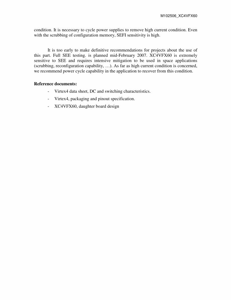
Appendix 1: Electrical interfaces
Daughter board to main interface
FX60 Daughter Board interfaces with the main board, High Speed Digital Tester (HSDT), via 1156-pin Hi-Lo connector. There are TBD numbers of general purpose I/Os available for user. I/O standard can be any of Xilinx defined I/O standards. Beside general purpose I/Os, there are 8 data lines and 6 control lines available for Select MAP programming of FX60. Figure 1 depicts the block diagram of FX60 test setup electrical interface.
Hi-Lo Interface
FX60
JTAG Header
PROM
Mode Select
External Power
(Optional)
General I/O
Select MAP
Power
Power Supply Power Supply or DMM
(Optional)
PC
Interface (RS232)
Program Voltage
Regulator (PT6701)
JTAG
Header
Hi-Lo Interface
FPGA (VII-Pro)
PROM
Voltage Regulators
HSDT
Controller (PC)
GPIB (PC)
Programmer
(PC)
Figure 1. Block Diagram of FX60 Test Setup Electical Interface
For Heating Unit
Heating Unit
FX60 Daughter Board
Thermistor/IR Dector
FX60 Daughter board Besides Hi-Lo interface connector to HSDT, JTAG programming connector,
Mode pins, and power supply connections are available for external connection. JTAG program connector is a 6-pin single strip header that can be connected to
PC via programming cable. JTAG connector is used to program the PROM (XCF32P) on the daughter board as well as FX60.
Mode pins select the FX60 programming mode, either Select MAP Program or Serial PROM Download. Mode pins are pull up jumpers that can be grounded using shorting plugs. HSDT can also select the programming mode if the jumpers are removed. This will allow the user to control the mode remotely.
Heating coils may be placed along the edge of FX60 if needed. This is to test the device at elevated temperature for latch up condition. High power resistors or Thermofoil heaters from Minco will be used for heating coils. The temperature of the device will be monitored by either thermistor or IR detector and controlled by the power supply to the coils.
M102506_XC4VFX60
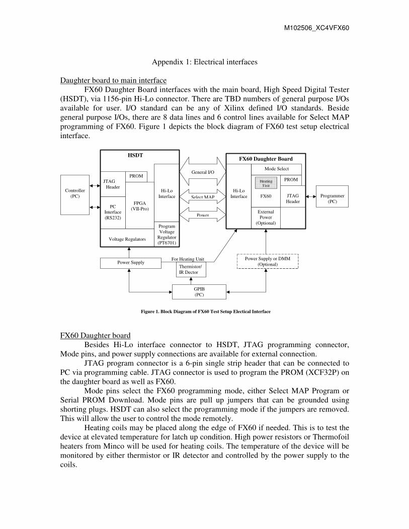
The daughter board requires four power supplies (3.3V, 2.5V, 1.8V, and 1.2V) to FX60 and peripheral devices such as PROM and SRAM. The daughter board can be powered up by the HSDT’s programmable voltage regulators (PT6701) or by external power supplies. HDST supplies the power to the daughter board via Hi-Lo connector. Each supply line from Hi-Lo connector has set of jumpers in series. When these jumpers are shorted, the daughter board gets power from the HSDT regulators. The jumpers can be used to monitor device currents using a digital multi-meters in series or by using shunt resistors. To supply power to FX60 using external power supply, the shorting jumper should be removed and the required power should be connected to the jumper pins. Figure 2 shows the power options for FX60 daughter board.
Hi-Lo Interface
FX60 Daughter Board
In-Line Headers
From HSDT
To FX60 and others
Place jumper to enable power route from HSDT. DMM in series / or shunt resistor can be used to monitor current.
Jumpers may be removed and external supply can be brought in via these pins.
Figure 2. Power Options for FX60 Board
HSDT Connection
HSDT board is powered by single +5V supply via BNC. Onboard regulators will convert +5V to supply necessary powers to the board.
HSDT has RS232, USB and Ethernet connections for communication with an external PC. The PC is the controller that commands HSDT and collects data from HSDT. For the initial test of FX60, RS232 will be used.
HSDT’s main processor (VirtexII-Pro) can be programmed using JTAG connector or onboard PROM. The PROM is programmed via JTAG as well. JTAG connector for the HSDT is also a 6-pin single strip header.
M102506_XC4VFX60
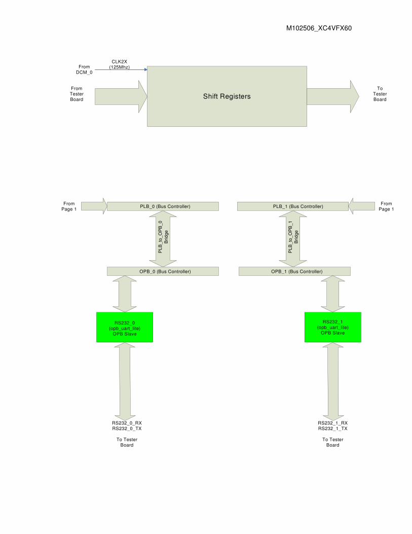
Appendix 2: DUT design, block diagram
PPC405_0Processor
PPC405_1Processor
PLB_0 (Bus Controller) PLB_1 (Bus Controller)
Dat
a S
ide
: P
LB M
aste
r
PLB_BRAM_IFACE_0PLB Slave
PLB_BRAM_IFACE_1PLB Slave
Block_Ram_0 Block_Ram_1
PLB_EMC_0(SRAM Controller)
PLB Slave
PLB_EMC_1(SRAM Controller)
PLB Slave
JTA
G In
terf
ace
JTAG Port
ResetControl
0
ResetControl
1
CEn, OEn, WEnADDR(0 to 20)
DQ(0 to 15)To DUT Logic and
External SRAM Block 0
CEn, OEn, WEnADDR(0 to 20)
DQ(0 to 15)To DUT Logic and
External SRAM Block 1
PPC_0_Reset PPC_1_Reset
DCM_0
To Clock Trees
CLK_0
To DUT Logicppc405_0_C405DBGWBIAR_pin(0 to 29),
ppc405_0_C405DBGWBFULL
To DUT Logicppc405_1_C405DBGWBIAR_pin(0 to 29),
ppc405_1_C405DBGWBFULL
ToPage 2
ToPage 2
Inst
ruct
ion
Sid
e :
PLB
Mas
ter
Inst
ruct
ion
Sid
e :
PLB
Mas
terD
ata
Sid
e :
PLB
Mas
ter
TODUT Logic
TODUT Logic
TODUT Logic
TODUT Logic
DCM reset
CriticalInterrupt_0
Non-Critical
Interrupt_0Critical
Interrupt_1
Non-Critical
Interrupt_1
EdgeDetect
EdgeDetect
EdgeDetect
EdgeDetect
M102506_XC4VFX60
PLB_0 (Bus Controller) PLB_1 (Bus Controller)FromPage 1
FromPage 1
PLB
_to_
OP
B_0
Brid
ge
PLB
_to_
OP
B_1
Brid
ge
OPB_0 (Bus Controller) OPB_1 (Bus Controller)
RS232_0(opb_uart_lite)
OPB Slave
RS232_1(opb_uart_lite)
OPB Slave
RS232_0_RXRS232_0_TX
To Tester
Board
RS232_1_RXRS232_1_TX
To Tester
Board
Shift RegistersTo
TesterBoard
FromTesterBoard
FromDCM_0
CLK2X (125Mhz)
M102506_XC4VFX60
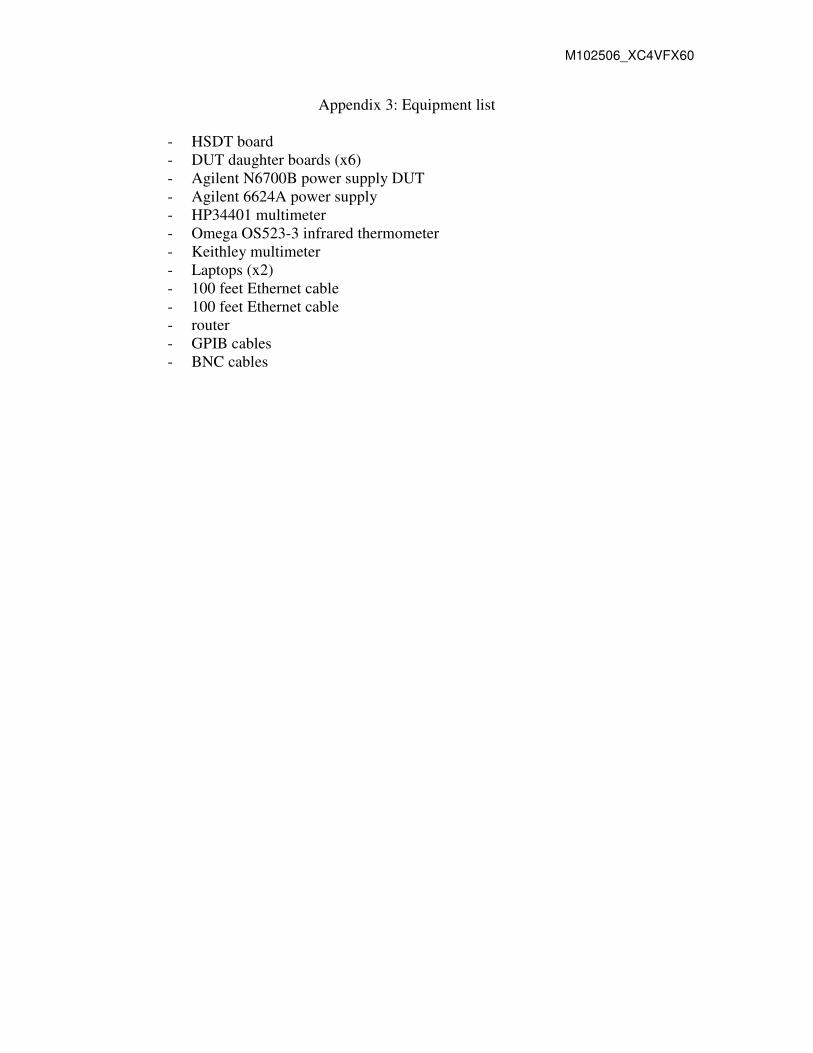
Appendix 3: Equipment list
- HSDT board - DUT daughter boards (x6) - Agilent N6700B power supply DUT - Agilent 6624A power supply - HP34401 multimeter - Omega OS523-3 infrared thermometer - Keithley multimeter - Laptops (x2) - 100 feet Ethernet cable - 100 feet Ethernet cable - router - GPIB cables - BNC cables