Embed Size (px)
Citation preview
.....
~ cl
(a) incorrect connections of totem pole TTL gates
A B
8--0--
{'" I ~ V
(b) open collector NAND gate
(c) open collector symbols
FIGURE 12.29 Open collector TTL NAND gate.
I I l 'i V
1. :: ul · · ~ 11 ' 111111
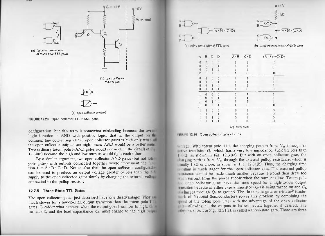
;on fi guration, but this term is somewhat misleading because the o\ 1 1 ·•II logic function is AND with positive logic; that is, the output till ti t common line connecting all the open collector gates is high only wl11 11 •tl the open collector outputs are high; wired AND would be a bell <.: • 1111111
Two ordinary totem pole NAND gates would not work in the circuit 111 II 12.30(b) because the high and low outputs would fight each other.
By a similar argument, two open collector AND gates (but n(>t lllll 11
pole gates) with outputs connected together would implement tlw lll i! tion F = A· B · C · D . Notice also that the open collector configtll tili•tt can be used to produce an output voltage greater or less than I ht supply to the open collector gates simply by changing the external VIl li ·•t connected to the pullup resistor.
12.7.5 Three-State TTL Gates
The open collector gates just described have one disadvantage: Tilt \' 11! much slower for a low-to-high output transition than the totem polt• 'I i I gates. Consider what happens when the output goes from low to high I ' · I turned off, and the load capacitance CL must charge to the high o111p11
II
I I
(A·B)·(C·D)
(11) 1/SIII J< l 'll lll' <' lllio llal TTL gates
A 13 c 0 () ()
() () 0 () 0 I 0 ()
() I ()
() I 0 I) I I 0
0 0 0 0 0 I 0 I
l 0 l 0 l 1 L l
D
()
I ()
0 I ()
0 I 0 I
0 l 0 I
A·B C·D
I
0 0 0 0
I I ()
1 1 1 0
1 1 1 0
1 1 1 0
(c) truth table
(1 111111 : 12.30 Open collector gate circuits.
I I 1 '1 \1 1.
:: I k!l
A :I ()(" 13
(A· B)· (C ·D)
c oc D
(b) using open collector NAND gates
(A· B)· (C· D)
l l l 0
l l l 0
l l l 0
0 0 0 0
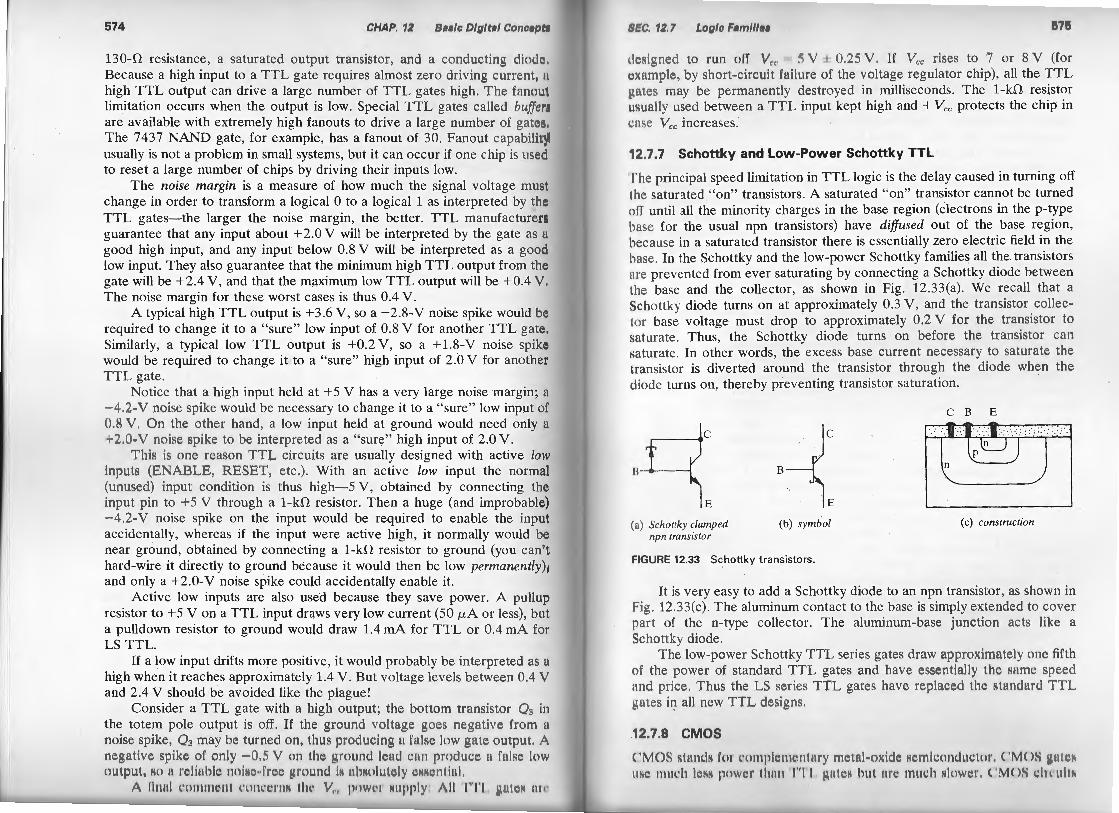
" ll llgt·. With totem pole TTL the charging path is from Vee through an 11 II \ 1 transistor Q4, which has a very low impedance, typically less than IIIII 0 , :•s shown in Fig. 12.31(a). But with an open collector gate, the II 11 p,i11g path is from Vee through the external pullup resistance, which is
1111 dl y I kH or more, as shown in Fig. 12.3l(b). Thus, the charging time !ll ll l11 11t is much larger for the open collector gate. T he external pullup
1 ~ ltutcc cannot be made much smaller because it would the n draw too ·IIII I II current from the power supply when the output is low. Totem pole ·lid llJH'II collector gates have the same speed for a high-to- low output ilt!ll ~ l t l nn because in either case a transistor (Q3) is being turned on and C~_ (I; 1 l11 u ges through Q3 to ground. T he three-state gate or tri~tat e09 (trade
·11 111 nl' National Semiconductor) solves this problem by combining the I'' 1 d ol' the totem pole TTL with the advantage of the open <.:o ll e<.: tor
11 1 11llowing all the outputs to be connected toge ther if dcsin,;d . T he llltl tl ll , shown in Fig . 12.::\ l (c), is ca lled a three-state ua tc . There an: thn:"
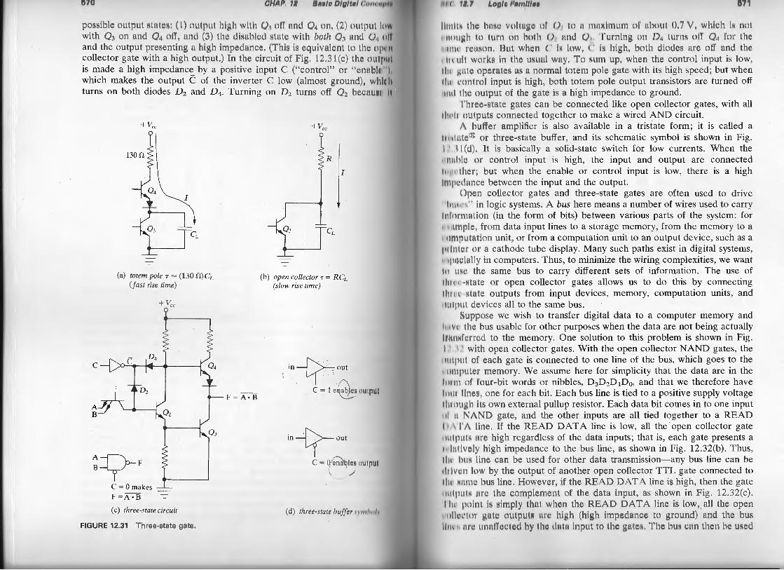
/II r ~IIA/' r • /1 111•lr1 OIIJIIIIII :uw,"l''
possible (llltput stutl•N: (I) uutput hi p, II with () 1 off ll 11 tl (),1 on, (2) output "''' with 0 3 on and 0 4 oil', nnd (.1 ) thu disabled ~Hnll.: with lw tlt (), und () 1 ttll and the output presenting u high impudancc. (This is equiva lent to tlw 1 'I'' 11
collector gate with a high output.) ln the circu it o f Fig. 12 .3 1 (c) the o utput is made a high impedance by a positive inpu t C ("control" or " cnHhli " t which makes the output C of the inverter C low (almost ground), wli lt It turns on both diodes D 2 and D 4 . Turning on D 2 turns off 0 2 bc<.: IIII IH It
c
A B
+vee
(a) totem pole T = (130 O)CL (fast rise time )
+ V, .,.
~v-F C = 0 makes F=A•B
(c) three-state cirwit
FIGURE 12.31 Th ree-state gate.
F= A•B
+Vee
R
CL
(b) open collector T = RCL (slow rise time)
-{f-out in
I ( b·lcs nul pill C=le~ ·
'"To"' C = 0 enJI;!Ics ou ll' lll
\
(J) th rl'i' ·.l'tll tl• lmjJI•r ,1'\'111/ln /1
/ ,tlt// 11 1'1111111. ·d
lliult 11 till' hliNl ' voltllp,t• ol 1_1 , to li IIIH XI nlltnl ol' nhout 0.'/ V, whkh IH not 1 tll llll',h to tum 011 both /) , 1111d () 1• 'l'uruing o n 1),1 turns o fl' 0 ,1 for the
IIIII ' ll'I INOII. 1\111 whun l ' is low, ( -. is high, both diodus ar..; off and the 1 111 uil work s in lhu usuul wny. 'l'o sum up, when the contro l in put is low, tilt p, ulu op~,;ratcs as a normal totem pole gate with its high speed; but when tl11 I'Onlrol inpu t is high , both totem pole outpu t transistors are turned off 111d the- outpu t of the gate is a high impedance to ground.
' I 'hn.:u-stat:e gates can be connected like open collector gates, with all tll t 11 nutputs co nnected together to make a wired AND circuit.
1\ hufl'e r amplifier is also available in a tristate form; it is called a It l'i lll lt•00 or three-state buffer, and its schematic symbol is shown in Fig. I 1 I I (d) . It is basically a solid-state switch for low currents. When the lltlll ll' or control input is high, the input and output are connected
!II)J.I ' tlu.: r; but when the enable or control input is low, there is a high tll)lt ldlln <.:e between the input and the output.
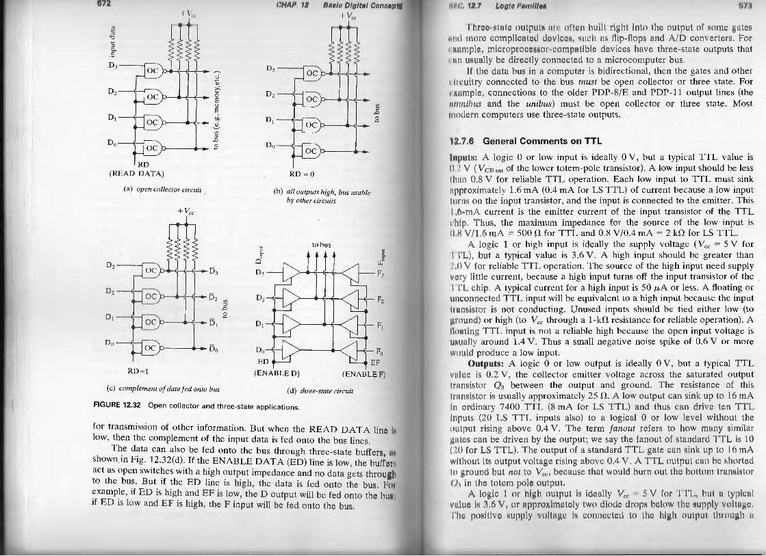
< )p~,; n collector gates and three-state gates are often used to drive I1!1Nt'H'' in logic systems. A bus here means a numberof wires used to carry
ulllt nmtion (in the form of bits) between various parts of the system: for lllt ph.:, from data input lines to a storage memory, from the memory to a
, " IIIJ !IIlatio n unit, or from a computation unit to an output device, such as a 111 lllli ' l' o r a cathode tube display. Many such paths exist in digital systems, l l jll ' t' iu lly in computers. Thus, to minimize the wiring complexities, we want 1' 1 1 INl' the same bus to carry different sets of information. The use of tllt l'tl· Ntate or open collector gates allows us to do this by connecting till I •' · state outputs from input devices, memory, computation units, and lt liljlt lt de vices all to the same bus.
S11ppose we wish to transfer digital data to a computer memory and li!1Vt' I he bus usable for other purposes when the data are not being actually 111111Nf't·r red to the memory. One solution to this problem is shown in Fig. I 1 11 with open collector gates. With the open collector NAND gates, the
11 11lp11 1 of each gate is connected to one line of the bus, which goes to the 1 11 111 p11t e r memory. We assume here for simplicity that the data are in the 1111111 ol' four-bit words or nibbles, D 3D 2D 1D 0 , and that we therefore have 111 111 lit ws, one for each bit. Each bus line is tied to a positive supply voltage tlll tll tp,h its own external pullup resistor. Each data bit comes in to one input ' II 11 NA ND gate, and the other inputs are all tied together to a READ I I \ J'A line. H the READ DATA line is low, all the open collector gate 1111lput s arc high regardless of the data inputs; that is, each gate presents a t l lll llw ly high impedance to the bus line, as shown in Fig. 12.32(b). Thus, 1! 11 ll us line can be used fo r other data transmission-any bus line can be 1lt iVt ' ll low hy the output of another open collector TTL gate connected to tlu Nlllnl' bus line. However , iJ the READ DATA line is high, then the gate 1\lllp ttt s ;1r0 the compl(; lrtent of the data input, as shown in Fig . 12.32(c). ll11 pnint is si111ply th nl whe n the READ DATA line is low ,, all the open
1 ·ll llt ~ t · tnl ' p,till' outp1 1t N IIH' high (high impcd;~nce to ground) and th ~.: bus liiii 'H ll l' ll unull'vi'll'd hy lilt• duln input to lh~ g11t es . 'l'lw hus r nn thun lw used
,, I\ ',
,\':! I' 1 t I "' "0
= ~,... .. _ .. .. _ ,.!"
a.
= 03
02
o,
u Q) :>, .... 0 E <!)
E oil ~
"' ;::l .0
b ... .9
RD (READ DATA)
(a) open collector circuit
+vee
o,£TTID, I), " .. - i), . - "'
;::l ..0
:.:~:: .9
RD=l
(c) complement of data fed onto bus
t:/11\1' 1:1 111111111 IJf1tU11/ l:ullllt!l•l• I \1,
I. r.t .l 0 3
Dz
~ .0
o,~ II E
~ cS OJ
Dz
o,
Do
o,,~b ...
RD=O
(b) all outputs high, bus usable by other circuits
to bus
ED
(ENABLE D)
(d) three-state circuit
8. w:_.S
F,
1": ,
F,
I'll
FIGURE 12.32 Open collector and three-state applications.
for transmission of other information. But when the READ DATA line I low, then the complement of the input data is fed onto the bus lines.
The data can -also be fed onto the bus through three-state butlers, 11 shownin Fig. 12.32(d). If the ENABLE DATA (ED) line is low, the bufl'1·to· act as open switches with a high output impedance and no data gets thr0111dt to the bus. But if the ED line is high, the data is fed onto the bus. llt11 example, if ED is high and EF is low, the D output will be fed o nto th l.) hti N_ if ED is low and EF is high, the F input will be fed on lo l'he bus.
I ~~ rl., ,, '/ ,1
'l' lll'lW ~ tlltl• t111tp11t ~ IIi! ' t~lli ' l l ilull1 light into the Ot11put 01' HOIII I.! )!tl ti..:S 111HI IIHH'c t· outpl h.: ntl\d th • vk~·H, ~ tll'II a l-l llip-llops aud A/1) <.;O uv l.) rtl.)rs. (lor 1 ~1 1111pl<:, tlli l.! roprocuHNol' •l'0111pltlihh; d l.) vil.!~.;s have three-sta te o utputs that 11111 w111a ll y be direc tl y co tln U<.; tcd to a microcomputer bus.
If the data bus in a computer is bidirectional, then the gates and other 1 l~t • tlitry connected to the bus must be open collector or three state. For 1 \ ll lllplc, connections to the older PDP-8/E and PDP-11 output lines (the Illllll llm.s and the unibus) must be open collector or three state. Most IIHH ic rn computers use three-state outputs.
n .7.6 General Comments on TTL
hllllll.s: A logic 0 or low input is ideally 0 V, but a typical TTL value is II 1 V ( V cEsat of the lower totem-pole transistor). A low input should be less ll 11 111 0.8 V for reliable TTL operation. Each low input to TTL must sink 11pproximately 1.6 rnA (0.4 rnA for LS TTL) of current because a low input 1111 us on the input transistor, and the input is connected to the emitter. This I !1-111 A current is the emitter current of the input transistor of the TTL 1 hip. Thus, the maximum impedance for the source of the low input is I I K V /1.6 rnA = 500 fl for TTL and 0.8 V /0.4 rnA = 2 kfl for LS TTL.
!\ logic 1 or high input is ideally the supply voltage (Vee = 5 V for ' I'TL), but a typical value is 3.6 V. A high input should be greater than
1 , () V for reliable TTL operation. The source of the high input need supply Vt••·y little current, because a high input turns off the input transistor of the 1"1'1 , chip. A typical current for a high input is 50 ~-tA or less. A floating or 1111 ~·onoected TTL input will be equivalent to a high input because the input I111 11 Sistor is not conducting. Unused inputs should be tied either low (to 1 ~ 1 ·o und) or high (to Vee through a 1-kfl resistance for reliable operation). A II oa t ing TTL input is not a reliable high because the open input voltage is ll ~ lllt lly around 1.4 V. Thus a small negative noise spike of 0.6 V or more Wti Uid proauce a low input.
Outputs: A logic 0 or low output is ideally 0 V, but a typical TTL vu luc is 0.2 V, the collector emitter voltage across the saturated output 1111 nsistor Q3 between the output and ground. The resi.stance of this l1 1111sistor is usually approximately 25 fl. A low output can sink up to 16 mA l11 ordinary 7400 TTL (8 rnA for LS TTL) and thus ca n drive ten TTL l11 pu ts (20 LS TTL inputs also) to a logical 0 o r low level without the tll ltput ri s.ing above 0.4 V. The term fanout refe rs to how mnny similar ltlltcs ca n be driven by the output; we say the fanout o f slandnrd 'I''I'L is 10 ( JO for LS TTL). T he output of a standard TTL ga tu can si 11k up to 1(, mi\ wi lhout its output voltage rising above 0.4 V. !\TTL o ulput ra n lw siHirtccl lo wound but not to v,.,., because tha t wo uld burn out tht· hotllllll IIIIII HiH tor 11, in I he tolc•n pole ou tput.
!\ logic I or high output is idea ll y V,... 5 V fo r '1"1 '1 ,, hut 11 lypl l'ld v11 lu~· is ;\,() V, or II PI H'oxiull•li •ly two dioik dmps lx·low tlw N11ppl y vo llngt·. 'l' h<· poHitivt· rm ppl y voll tqw iN i'llltoerlt'd to thl' hig h llt ltpul llu 11 111 lh 11
574 CHAP. 1 IJIIIIIC D/g/(11/ Ctm tJtJIJI
130-!1 resistance, a saturated output transistor , and a conducting diodl' . Because a high input to a TTL gate requires almost zero driving current , 11
high TTL output can drive a large number of TTL gates high. T he fanout limitation occurs when the output is low. Special TTL gates ca lled bujft•t,\' are available with extremely high fanouts to drive a large number of ga tes . The 7437 NAND gate, for example, has a fanout of 30. Fanout capabilit y usually is not a problem in small systems, but it can occur if one chip is used to reset a large number of chips by driving their inputs low.
The noise margin is a measure of how much the signal voltage must change in order to transform a logical 0 to a logical 1 as interpreted by tlw TTL gates- the larger the noise margin, the better. TTL manufacturers guarantee that any input about +2.0 V will be interpreted by the gate as a
good high input, and any input below 0.8 V will be interpreted as a good low input. They also guarantee that the minimum high TTL output from the gate will be +2.4 V, and that the maximum low TTL output will be +0.4 V . The noise margin for these worst cases is thus 0.4 V.
A typical high TTL output is +3.6 V, so a -2 .8-V noise spike would be required to change it to a "sure" low input of 0.8 V for another TTL gate. Similarly, a typical low TTL output is +0.2 V, so a +1.8-V noise spik<.: would be required to change it to a "sure" high input of 2.0 V for another TTL gate.
Notice that a high input held at +5 V has a very large noise margin; a - 4.2-V noise spike would be necessary to change it to a "sure" low input of O.H V . On the other hand, a low input held at ground would need only a 12.0- V noise spike to be inte rpreted as a "sure" high input of 2.0V.
This is on<.; reason TTL, circuits are usually designed with active low input s (E NAB LE, RESET, etc.). With an active low input the normal (unused) input condition is thus high-5 V, obtained by connecting the input pin to +5 V through a 1-kD resistor. Then a huge (and improbable) - 4.2-V noise spike on the input would be required to enable the input accidentally, whereas if the input were active high, it normally would be near ground, obtained by connecting a 1-kn .resistor to ground (you can' t hard-wire it directly to ground because it would then be low permanently) , and only a +2.0-V noise spike could accidentally enable it.
Active low inputs are also used because they save power. A pullup resistor to +5 Von a TTL input draws very low current (50 p.,A or less), but a pulldown resistor to ground would draw 1.4 rnA for TTL or 0.4 rnA for LS TTL.
If a low input drifts more positive, it would probably be interpreted as a high when it reaches approximately 1.4 V. But voltage levels betwee n 0.4 V and 2.4 V should be avoided like the plague!
Consider a TTL gate with a high output; the bottom transistor 0.1 in the totem pole output is off. If the ground voltage goes ncg.1tive from 11
noise spike, 0: .. may be turned o n, thus producing n fal se low gat ~.: oulpul. ;\ negative spike of only 0.!-i V on the ground knd cu rl pr·odllt't: 11 f :~ l sL' low 0 11tp11t , SO II ~t • l l uhll' lllllHl' l' n •l· j',l'll llllll lN UbNrtlll!i' ly l : ~ll-l l' llt lnl.
1\ il11 11 l l ' lllllllllllt I'HIH'I ' III H tl11 • \1., (lli WI ' I ll llppl y • /\ II '1"1'1.. )•. ll t t ~H 111 1'
IJC. 1~ . l.u nu/1, 1
dl'Nig ned to run ofl' V,. '1 V I 0.25 V . If V,.c rises to 7 or 8 V (for l'X:tmplc, by short-c ircuit failure of the voltage regulator chip), all the TTL p, u t ~s may be permanently destroyed in milliseconds. The 1-kn resistor usua lly used between a TTL input kept high and +Vee protects the chip in l' IIS<..: Vee increases.
12.7.7 Schottky and Low-Power Schottky TTL
T he principal speed limitation in TTL logic is the delay caused in turning off the saturated "on" transistors. A saturated "on" transistor cannot be turned ofi until all the minority charges in the base region (electrons in the p-type base for the usual npn transistors) have diffused out of the base region, because in a saturated transistor there is essentially zero electric field in the base . In the Schottky and the low-power Schottky families all the transistors 1re prevented from ever saturating by connecting a Schottky diode between the base and the collector, as shown in Fig. 12.33(a). We recall that a Schottky diode turns on at approximately 0.3 V, and the transistor collector base voltage must drop to approximately 0.2 V for the transistor to saturate. Thus, the Schottky diode turns on before the transistor can saturate. In other words, the excess base current necessary to sa turate the transistor is diverted around the transistor through the diode when the diode turns on, thereby preventing transistor saturation.
I .c
ll ' I
E
(a) Schottky clamped npn transistor
c
B
E
(b) symbol
FIGURE 12.33 Schottky transistors.
C B E
(c) construction
It is very easy to add a Schottky diode to an npn transistor, as shown in l<'ig. 12.33(c). The aluminum contact to the base is simply extended to cover part of the n-type collector. The aluminum-base junction ac ts like a Schottky diode.
T he low-power Schottky TTL series gates draw approximately one fifth of the power of standard TTL gates and have esse ntia ll y the san•~.: speed und price. Thus the LS series TTL ga tes have replacud the stnndar·d TTL ga tes i~ all new TTL dcsi!!ns.
.12.7.8 CMOS
( 'MOS NtnndN I'OJ l 'lllnph II H' IIt iii Y nwl :tl -oxide 14\' lll il'orulueto r , ( 'M< >S gnt1:
li Nt' rnllt 'h lmoi'l po Wt ' l thn11 '1''1'1 g r •t t ~N hul l ll'l ' 11111 \' h NIOWI ' I . c 'M< >S l'iH ~ II l l ti
576 CIIA/'. 'I /IIIHia Dlnf'l'll l Clllll'hl'
use both n-c hannc l and p-channt;l cnhanccmcnt MOSFE'I'~ in " t ' ll lll
plementary" pairs. Extremely low power consumption is ac hieved l>l' l ' ll ll ~ •
power is consumed only when the circuit is switch ing states- not whih- tit• circuit is in the steady state. Other advantages include larger noise lllllt l',lll
relative immunity to temperature fluctuations, operation from +3 to I H \ voltage supply, and a large fanout capability.
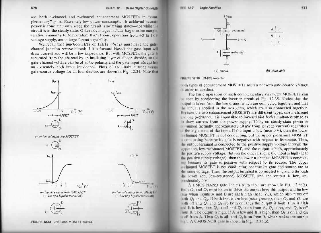
We recall that junction FETs or JFETs always must have tht p,1 1t1 channel junction reverse biased; if it is forward biased, the gate input wil l draw current and will be a low impedance. But with MOSFETs the g11t1 t separated from the channel by an insulating layer of silicon dioxide, Nn tit• gate-channel voltage can be of either polarity and the gate input alwCI)IS II <~
an extremely high input impedance. Plots of the drain current VI t llll
gate-source voltage for all four devices are shown in Fig. 12.34. Not v ll !itl
llol
--3 Vcs (V) n-channel J FET
G~: or n-cllllnnd dcplclion MOSFET
G~ llol
1 2 3 Vcs (V)
n-channel enhancement MOSFET (-like npn bipolar transistor)
~ FIGUHE 1Z.ll4 .IPI I dtHI MO::PI''I llt iiVI ... .
llol
Vos (VI p-channel J FET
G~:
llol
\ ', 1 I
p -channel enhtlll t('lll l' lll Ml J,\/1 I ( - like pnp bipo /ar l riiii,I/1/Htl
11. I / ,llf/(11 /1111111/11 l/'1
I I'"'
j~ (i l ~ r -channcl
I-F= A
G I :r '"'"''"'' * I
0 A--+
(a) circuit (b) truth table
llt lllltl 1l.35 CMOS inverter.
l11tll1 typ~.:s or enhancement MOSFETs need a nonzero gate-source voltage 111 '" dt ·r to conduct.
l'lw basic operation of such complementary symmetry MOSFETs can l!!J IU't' tl by considering the inverter circuit of Fig. 12.35. Notice that the iltl put iH taken from the two drains, which are connected together, and that
llil Inpu t is applied to the two gates, which are also connected together. iII • Ill I N~· the two enhancement MOSFETs are different types, one n-channel 1111 1 •II H' p-channel, it is impossible to forward bias both simultaneously so as 1 1 ti111W current from the power supply. Thus, no steady-state power is " " ~· llllll'd (actually approximately 10 nW from leakage current) regardless
til till' logic state of the input. If the input is low (near 0 V), then the lower it 1 lt 11 11lli.:l MOSFET is not conducting, but the upper p-channel MOSFET I ~ , IIIH iucting because its gate is negative with respect to its source. Thus, il11 1111 tptlt terminal is connected to the positive supply voltage through the 111'1'' 1 (on, low-resistance) MOSFET, and the output is high, approximately til• pnNitive ~upply voltage . But, on the other hand, if the input is high (near tit• pnt~ itivc supply voltage), then the lower n-channel MOSFET is conductiliJI l~t • t 'l lllse its gate is positive with respect to its source. The upper I ' • l:un nl'l MOSFET is not conducting because its gate and source are at lito 111 1111~· volt age . Thus, the output terminal is connected to ground through 1111 ltlW~\ r (on, low-resistance) MOSFET, and the output is low, apl" "'i llllllcly 0 v.
A ( 'MOS NAN D gate and its truth table are shown in Fig. 12.36(a). IIIII It ()I and o~ must be on to drive the output low; this output will be low ~til l Y wht·n input's !\ and B arc each high (near Vee), which also turns off l•,oth (} 1 nnd Oz. If both inputs arc low (near grou nd), then 0 3 and 04 are iuttlt nlh:nd 0 1 and (), an.: both on; thus the output is high. H A is high 111ol II i ~t low, tht·n (), is o il' 11 11d Q., is on from /\ , 0 2 is on, and 0 4 is off
11,•1111 II. ' l'lw ou tp11t IH high , II' A iH low 11 11d II is high, tl1 ~.: n 0 1 is on t~nd 0 1
t odl I'IIHII A. 'l'htlli ('·IN 1111' , lll ld (),, IH 0 11 1'1'(1 111 1\, whkh lllllk t•H th ..: (llltpnt ltl J' II A C'M<>S N<>H )\ll tt• iHN h~tWII i11 l •'lg . 1/ , ll,(h) .
578 CHAP. 12 Basic Digital Concepts
.__--------<E-------~~--- F = A • B A_.--------------~-----,
A B 01 Oz 03 04 F
8--------------~----~ 0 0 on on off off I
0 1 on off off on I
1 0 off on on off I
(a) NAND (e.g. , 74COO) 1 1 off off on on ()
A--~----------~
B~;---::-----~--...,
.....--J, + F=A+B
A B 01 Oz 0 3 04 ,, 0 0 off on on off
0 1 off on off on II
1 0 on off on off I I
1 1 on off off on II (b) NOR (e.g, 74C02)
FIGURE 12.36 CMOS NAND and NOR gates.
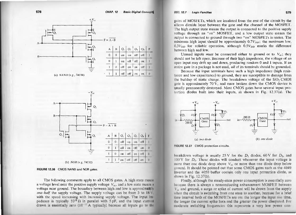
The following comments apply to all CMOS gates. A high sta te 1111' 111 1
a voltage level near the positive supply voltage Vee, and a low state nWI III I-o ,, voltage near ground. The boundary between high and low is approxi uudrh one-half the supply voltage. The supply voltage can be from 3 to I H \ with the speed increasing wi th inc reas ing supply vo ltage. T he input 1111
pedance is typically 10 12 !1 in paralle l with 5 rF, and the input ~' llll rllt d raw n it< et<st nli a ll v /',~·ro ( I () 11 A typi!'u ll y) hl'\'ll ll S~· ull inpu ts go 111 ll u
C. 12.7 Logic Families 579
p.utes of MOSFETs, which are insulated from the rest of the circuit by the ilicon dioxide layer between the gate and the channel of the MOSFET. l'he high output state means the output is connected to the positive supply vollage through an "on" MOSFET, and a low output state means the output is connected to ground through two "on" MOSFETs in series. The ulinimum high input should be approximately 0.7V00 ; the maximum low, 0 \ V v v for reliable operation, although O.SV vv marks the difference lwtween high and low.
Unused inputs must be connected either to ground or to Vee; they hould not be left open. Because of their high impedance, the voltage of an
tllll.: n input may drift up and down, producing random 0 and 1 inputs. If an 1 1t1ire gate in a package is not used, all of its terminals should be grounded.
Because the input terminals have such a high impedance (high resisIIIIH:e and low capacitance) to ground, they are susceptible to damage from lhl' bu ildup of static charge. The breakdown voltage of the Si02 CMOS
li e is approximately 70 V, and once broken down the CMOS device is llll llltlly permanently destroyed. Most CMOS gates have several input proll'l"lion diodes built into their inputs, a's shown in Fig. 12.37(a). The
+Vee +Vee +Vee
II I + out m 1--t----- out
(a) two diode (b) one diode
lfl iJnE 12.37 CMOS protection circuits.
lt11 ukdown voltage is usually 25 V for the D 1 diodes, 60 V for D 2 , and 1110 V for 0 3 . T hese diodes will co nduct whe never the inpu t vo ltage is lll tttl ' than one diode drop above V ee or mo re than o ne d iode drop be low llllt lllitl. It sho uld be po inted o ut tha t some C MOS ga tes such <IS the 4049 IIVI' I ll'r a nd the 4050 buffe r conta in o nl y o ne input protut tio n d iode, as II11W II in l'ig. 12.37(b).
J!lnu ll y, althoug h the steady-sta te powe r consumpt k111 is l'NNl' lll ill ll y l':l.ii'O
lu1 1 ~11 1-lc there is always a no nc()nduc ting c nhwl t(; lliL' lll M( )~·11 •'11' 1 ' hl'lwu~.: n
I " find ground , 11 sm gt: Ol' spike o f current will he d ruw n l't n n 1 lil t• Hnppl 1!1 11 I ll ~· drt· uit is swi trld ng l' t' t) tll om· slute to lltlo tll l' l' , IWt 'I IIIHI' lu1 11 !Hid
tllllt ' 111 11'1 vu l bo th o l' 11 11' M( )S I•'H'I's Il l '(' o n : II H' lougt' l ll u· i11p111 1 tNt ' tin t\\ 1111 hulp.t•r tl w (' 1111 1' 111 Npilll' l llfiiH 1111d tl w 1\ll' llli' t II H' pt,WI' I d iHiilplllt d Fo1
llt lldt •l'll(i • NWill' li it iH It t '1111 Ill h•N iiJ IN ll 'pll 'HI ' IIIH II Vl ' l V low pttWt I tllll
580 CHAP. 12 Basic Digital Concepts
sumption on the order of microwatts, but as the switching frequency goes up the average power consumption also goes up. Each time the output changes from 0 to 1, the output voltage changes from 0 to Vee. and tlw output capacitance to ground must charge up to Vee. requiring energy CV~e/2. Thus the "switching" or "ac" power consumption is proportional to fCV~o where f is the frequency.
The fanout of CMOS gates is large because of the small input currents; one CMOS gate can typically drive 50 other CMOS gates.
The standard CMOS chips are numbered in the 4000 series; fo1 example, 4011 is a quad-two-input NAND gate, 4001 is a quad-two-input NOR gate, and 4049 is a hex inverter. The 54C or 74C series is also CMOS and is typically 50% faster than the 4000 series; for example, a 74COO is 11
quad-two-input NAND gate, and so on. Three-state CMOS gates m r available, as in TTL. There are no open collector CMOS gates as there a1' in TTL, but the CMOS family does contain "analog switches" (which Clll l
conduct current in either direction), which are unavailable in TTL. O ru such analog switch is the 4051, which can be turned on or off by a volta g1 input that need supply essentially no current. Also, the switch input ;nul output terminals can be interchanged just as for a mechanical switch.
12.7.9 Emitter-Coupled logic (ECL)
The ECL family is the fastest, with propagation delays from 0.75 to li n and operating frequencies up to several hundred megahertz. It is based 1111 transistors in the common base configuration with the outputs taken ofT tl u emitters, hence the name. The transistors are prevented from ever salUI III ing. The ECL family has a high fanout and operates from a negative supph voltage, Vee = -5.2 V or - 4.5 V. Its principal disadvantage is that !1 11 difference between the two logic levels is very small: A logic low is - I .7 \ and a logic high is - 0.9 V. Many different gates are available; the H< ' I family chips are numbered in the 10000 and the 100000 series.
12.7.10 High-Speed (HC) CMOS Family
The newest version of CMOS is the high-speed CMOS family or HC sv1 j, A high-speed CMOS quad NAND gate would be denoted 74HCOO uud 1
logically equivalent to a 74LSOO or 7400 chip. T he 74HCXX N1' ll•
combines the speed of the 74LSXX low-power Schottky TTL family Wil li
the low power consumption of the 74CXX CMOS or 4000 CMOS f:uulli• At this writing, as many chip types are available in the HC family 11t. 111
either the LS TTL or TTL families. Thus most new designs us<.: Il l\' li t family.
The high -speed of the HC fa mily is made possibl<.: by th <.: snud1L'1· we t;i the active area o f the chip. Supply vo lt ages ca n rnngc from 2 lo 6 V; t, Vi recomme nded. Bo th ':;ti.Jl ('XX (111 ilit:11'Y, :i'\" to l .~fi"(') :u1d 7·111 <'\
SEC. 12.7 Logic Families 581
(commercial , - 40° to 85°C) versions are available. The 74HCXX noise margin is not quite as good as for standard CMOS: minimum 3.15 V for a high input, and maximum 0.90 V for a low input.
The minimum high output is (Vee - 0.1 V), and the maximum low I>Lttput is O.lOV. HC D flip-flops can be clocked up to 30MHz with a 15-pF load and 20 MHz with a 50-pF load, and the clock-to- O output time Is only approximately 25 ns.
As with any chip, the junction temperature T1 inside the chip active 1naterial is given by
T1 = TA + P0 8
where T A = the ambient temperature, P0 = the power dissipation in watts, 1ud (J = the thermal resistance in degrees Celsius per watt of the chip. II = 130°C/W for most HC chips in a plastic DIP, and 8 ~ 100°C/W for a l'l'l"amic DIP.
A few precautions are in order for (HC) CMOS.
The input signal should have a transition time of less than 500 ns (from 0.1Vee to 0.9VeJ-
I Unused inputs should be connected to v ee or to ground. ' l'he vee power supply leads should be well bypassed. (' heck the flip-flop "hold time" requirement- the data must remain stable for a l'Crtain number of ns even after the active edge.
., The minimum high input required is approximately 3.1 to 3.5 V (compared to 2.0 V for TTL). This may be a problem when driving 74HCXX with 74LSXX If extra output current is drawn from the 74LSXX output. (The CMOS input •cquires only nA or less.) A pullup resistor may be necessary on the 74LSXX output or a driver/buffer between the 74LSXX output and the 74HCXX input.
11 As we can see from Fig. 12.37, the output voltage should never be more positive I ha 11 v ee plus one diode drop, or else the output diode Will conduct. Similarly the 1111lput voltage should never be more negative than one diode drop below f\ lil ll lld.
To avoid burning out either regular 74CXX CMOS or 74HCXX lii llh speed CMOS chips, observe the following rules :
Sltll'c in conducting (blac k) foam, neve r whi te foa n1. 1
11111 '1.' chips should be laid leads down o n a coruhlt li"R :w rfun: (nl l' lul). I hound solder ing iro n ti ps. 1'11• 11 o ff the power /Ji'f'Ori' ei ther insert ing or removi ng c hips. l k s;u·c. un used inpul s arc eilhcr grounded Il l' wired lo \1,. , ( I ll' l'fltd'ul nf ih" hl p,h llll pt:da nn ; ''o ff " o ul put of lhrcc-s lutc o ulpul s.)
'' 111 11 11 ~·x tn: nw l y " noisy" d~1l' l rirll i l' 11 Vi t ' l llllll \' lll 11 I 0 kH 111 lOll lt\111 •N IHIIIIII 'I' In I tit•.N Wil li lh\' lnp111 jllt1 VIdl'N \'OIINidVII Ihl\· JHO it•l' iiO II Ill lht• 1' \JII' IlNI ttl Nll )l hi ly
it•WI' I NJWl'd
582 CHAP. 12 Basic Digital Concepts
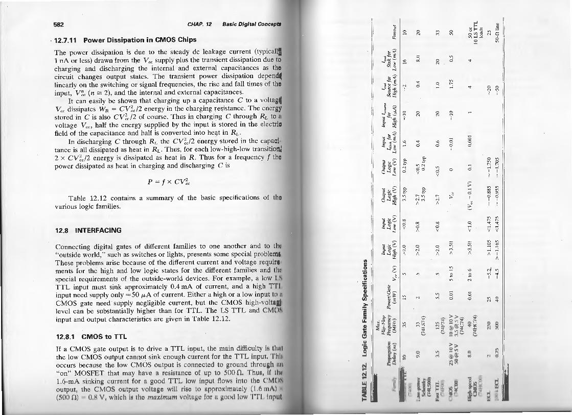
· 12.7.11 Power Dissipation in CMOS Chips
The power dissipation is due to the steady de leakage current (typically 1 nA or less) drawn from the Vee supply plus the transient dissipation due to charging and discharging the internal and external capacitances as tht.· circuit changes output states. The transient power dissipation depends linearly on the switching or signal frequencies, the rise and fall times of tlw input, V~e (n = 2), and the internal and external capacitances.
It can easily be shown that charging up a capacitance C to a voltagl· Vee dissipates WR = CV~e /2 energy in the charging resistance. The energy stored in Cis also CV~e/2 of course . Thus in charging C through RL to 11
voltage Vee. half the energy supplied by the input is stored in the electril' field of the capacitance and half is converted into he&t in RL.
In discharging C through RL the CV~e/2 energy stored in the capaci tance is all dissipated as heat in RL . Thus, for each low-high-low transition . 2 x CV~e/2 energy is dissipated as heat in R. Thus for a frequency f tlw power dissipated as beat in charging and discharging C is
p = f X CV2 ee
Table 12.12 contains a summary of the basic specifications of thl' various logic families.
12.8 INTERFACING
Connecting digital gates of different families to one another and to tIll "outside world," such as switches or lights, presents some special problem These problems arise because of the different current and voltage requi1 t ' ments for the high and low logic stat(;!s for the different families and tl w special requirements of the outside-world devices. For example, a low I TTL input must sink approximately 0.4 rnA of current, and a high '1''1'1 input need supply only =50 fLA of current. Either a high or a low input to 11
CMOS gate need supply negligible current, but the CMOS high-vo lt ltf\1 level can be substantially higher than for TTL. The LS TTL and C M< ~ ~ input and output characteristics are given in Table 12.12.
12.8.1 CMOS to TTL
If a CMOS gate output is to drive a TTL input, the main difficulty is tl1 11 1 the low CMOS output cannot sink enough curre nt fo r the TTL inpul. ' l'lt l occurs because the low CMOS output is conncctccl t:o ground through 11 11
"on" MOSFET that may have a res ista nce of up to 500 0. Thus, il' 11 11 1.6-mA sinking curre nt fo r :1 gno<l T Tl , low input llows int o the: < 'M< >' outpu t', l'hc CMOS output volta gt.· will l'i:<l' to upproximnk ly ( I ,(t tu Al
(500 0) O.H Y , whirh iH tl11 • 11111 ,.,,,,,,, vo lt llp.l' for 11 p.ood low 'I"I 'L 111p111
Ill c 0 ... 5
:;::: 'i:j Q) c.
CIJ
~ ·e Cll
LL Q) ... Cll (!) u
'g ...J
N ... N ... ~ ~
'ii ~ I o t2 ....
~~ ~ol<. E ~g~';' I~
"'.:l ~~
ol<.e; '5 ~--IN ~o ~...:: I
::< bO
r5l:i; . ~ ~
g ~ .... - ~ ::!. I 0 ~~:; II ft .~ ..., :t::
-6~ ::s"'-.E "'"~I'D ..:; .5 ~ ~
..... -.:l
t&,~IE: ::< <:) ~ ~ 0'"",.3 0
- ~, ~-~G ~ - bO -" ..3 "" v; 0 ~ c<i
'ii·~G I"'! """" ~ 0 ~ .:l.:l v
-u> :::·-~I 0 ~~...:: :--5
""'""~ 'I
~
"
~ u I v;
>-"
sg~lv; '" E ,... ~ ~
~
"'- "" "'" ~ >< G:: " "' I .,.,
" ' :lj ;I; "' ~ .9- ~~ i:i::Lt; ~
" ~ ·§5 00•
~~· I ~
0 N
0 oci
"" 0
0 N
"" 0
Q.
c V"lN 00 v
Q.
c <-v; NM 1\
00 0 1\
0 C"i 1\
v;
N
~
~§
C!
"'
"" c::.
"' "'
0 N
'=! ....
0 N
'D 0
v; 0 v
.N 1\
co 0 v
0 C"i 1\
v;
0 v;
v; 0
v; r-: ;....
:3 I
,...., 0 0 I
0
;}
v; c<i 1\
~ .9
...l ..,1- "' 0 r-- U'l c:: oCI:l ~ tn :.= v;,-l_2 N C:
""
""
,....,
.... g 0
0
> 0 I
·}
'=! .... v
v; c<i 1\
'D
.9
~ ~
0 0 N v; I I
0 v; v; 0 r--: r--: ........ I I I I
v; v; 00 v;
00 "' 0 0 I I I I
v; v; .- .-<!" "" ~ ......;
v v
on .,.,
~ ~ .... ,...., 1\ I
1\
N\ v; v) -.i-1 I
v; N
.... .... v; 0 0 v) 0 0
~ >>~ ~ .q- o 11jv O
~r;:: ;;;',@ D ~..,.. ~"d' ~ ..,. ~
,.;
c ~~c ~
> · ~ ~ (!V(Sj)
~I tf)
C!
1: I
v; 0 N '<t
584 CHAP. 12 Basic Digital Concepts
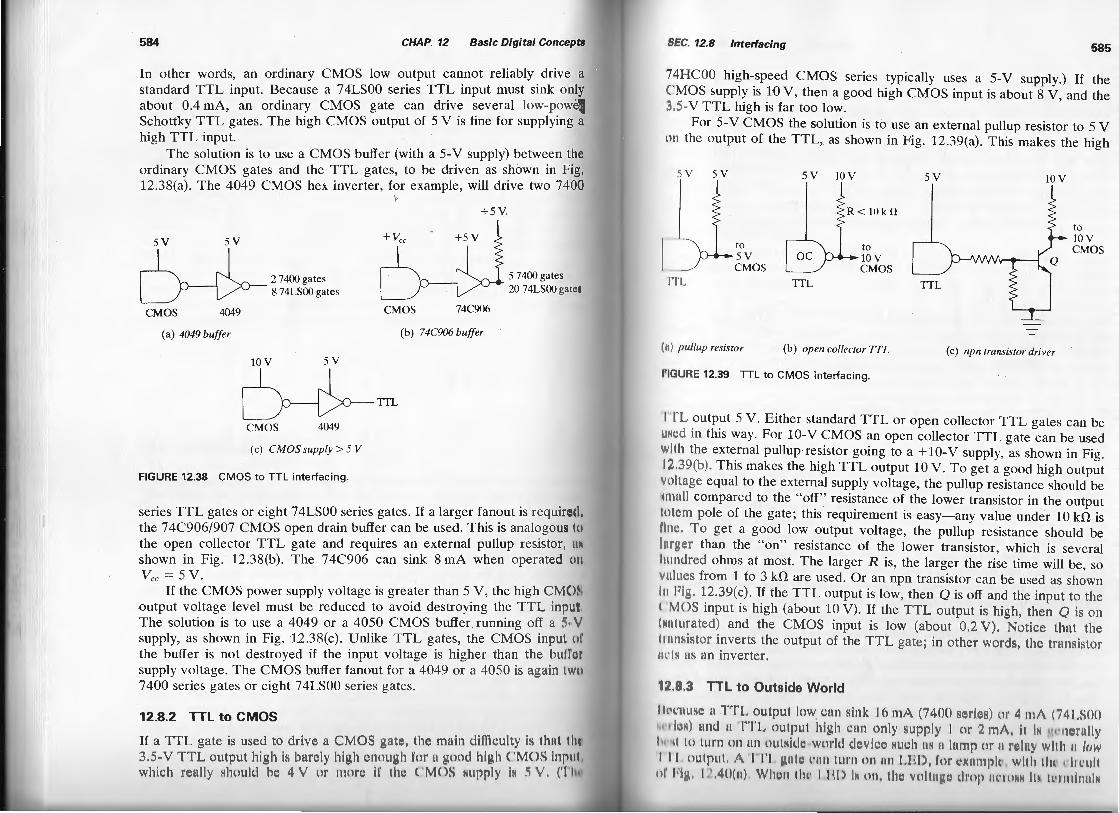
In other words, an ordinary CMOS low output cannot reliably drive a standard TTL input. Because a 74LSOO series TTL input must sink only about 0.4 rnA, an ordinary CMOS gate can drive several low-power Schottky TTL gates. The high CMOS output of 5 V is fine for supplyi~g a high TTL input.
The solution is to use a CMOS buffer (with a 5-V supply) between the ordinary CMOS gates and the TTL gates, to be driven as shown in Fig. 12.38(a). The 4049 CMOS hex inverter, for example, will drive two 7400
.,.
+SV
SV 5V
5 7400 gates 20 74LSOO gate~
2 7400 gates 8 74LSOO gates
CMOS 4049 CMOS 74C906
(a) 4049 buffer (b) 74C906 buffer
IOV 5V
TIL
CMOS 4049
(c) CMOS supply> 5 V
FIGURE 12.38 CMOS to TTL interfacing.
series TTL gates or eight 74LSOO series gates. If a larger fanout is requir~.:d ,
the 74C906/907 CMOS open drain buffer can be used. This is analogous 111 the open collector TTL gate and requires an external pullup resistor, 11
shown in Fig. 12.38(b). The 74C906 can sink 8 rnA when operated 011 Vee = 5 V.
If the CMOS power supply voltage is greater than 5 V, the high C M< l0 output voltage level must be reduced to avoid destroying the TTL input The solution is to use a 4049 or a 4050 CMOS buffer running off a 5 V supply, as shown in Fig. 12.38(c). Unlike TTL gates, the CMOS input 11l the buffer is not destroyed if the input voltage is higher than the bull'! 1 supply voltage. The CMOS buffer fanout for a 4049 or a 4050 is aga in IWII
7400 series gates or eight 74LSOO series gates.
12.8.2 TTL to CMOS
If a TTL gate is used to drive a C MOS gate, lhc rnain difli cull y is lhnl 1111 3.5-V TTL oulput hi gh is lx trcly high vnough l'or tl gPod high ( 'MOS l lipill which n.:nll y should Ill' ' I Y <!I" nHtn· if ti ll' < ' M( lS :o~ uppl y is C. Y . (' l 'l11
SEC. 12.8 Interfacing 585
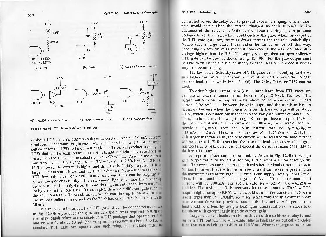
4HCOO high-speed CMOS series typically uses a 5-V supply.) If the CMOS supply is 10V, then a good high CMOS input is about 8 V, and the 1.5-V TTL high is far too low.
For 5-V CMOS the solution is to use an external pull up resistor to 5 V 1111 the output of the TTL, as shown in Fig. 12.39(a). This makes the high
5 v 5 v
I'I'L
to 5V CMOS
I 11 ) put/up resistor
5V IOV
TIL
to 10 v CMOS
(b) open collector TTL
IIGURE 12.39 TTL to CMOS interfacing.
5V lOV
(c) npn transistor driver
to lOV CMOS
·r 'I'L output 5 V. Either standard TTL or open collector TTL gates can be u s~.:d in this way. For 10-V CMOS an open collector TTL gate can be used wi th the external pullup resistor going to a + 10-V supply, as shown in Fig . I ) .:19(b). This makes the high TTL output 10 V. To get a good high output vol tage equal to the external supply voltage, the pullup resistance should be
1111tl l compared to the "off" resistance of the lower transistor in the output lotcn1 pole of the gate; this requirement is easy-any value under 10 kO is f1111.'. To get a good low output voltage, the pullup resistance should be l111 ga than the "on" resistance of the lower transistor, which is several hund red ohms at most. The larger R is, the larger the rise time will be, so vu lu<.:s from 1 to 3 kil are used. Or an npn transistor can be used as shown 111 Fig. 12.39(c). If the TTL output is low, then Q is off and the input to the c 'MOS input is high (about 10 V). If the TTL output is high, then 0 is on ("ll lur<llcd) and the CMOS input is low (about 0. 2 V ). No li e~.: I ha t the I1 1111 Nistor inve rts the output of the TTL ga te; in other words, the 11': 11\Sislor II 'IN 111-1 an inve rte r.
12.8.3 TTL to Out side World
l lt ' I'1 111 SC a '1''1'1 , o u1p111 low can sink 16 nt/\ (7400 se l'il' S) tll' •I 111 /\ ( / •II .SOO 1 1 h·s) :u td a '1''1'1 . output high enn only supply I or .!. 1n /\ , 11 11"1 gt' lll 'ndly
lw l'l l lo 111 1" 11 on 1111 lltll ~ id t· wodd dt•vi t'\' such ItS 11 l:uup 111 11 ~t • l ny Willi 11 I11W
' I 1'1, lllllptll, 1\ '1"('1 f:ll l t• III II 111111011 111 1 I,I IJ ) , f't ll I 'XI II Il j~lt •, Wi ll i i l l! I IJ t IIi I tt l flig . I.I ,•IO(n) , W lu•11 lil t• I Ill) IN 1111 , fl w vu ll lll\1! dl ll(l llllltNN i l "' It ll t li l lltl
586
+5Y
7400--> I LED 7437--> 5 LEDs
(a) LED
LED
+SY
74LSOO 7404 driver, etc
(d) 74LS(){) series with driver
CHAP. 12 Basic Digital Concepts
+5Y
7400
(b) relay
relay coil
+5Y
(e) pnp transistor driver
+15 v
relay coil
(c) relay with open co/lecwr
+5V
' (f) npn transistor driver
FIGURE 12.40 TTL to outside world devices.
is about 1.7 V, and its brightness depends on its current: a 10-mA curn·111 produces acceptable brightness. We shall consider a 10-mA cun'(' lll sufficient for the LED to be on, although 1 or 2 rnA will produce a dimly Ill LED that can be seen indoors but not in bright sunlight. The resistanCI' 111
series with the LED can be calculated from Ohm's law: Assume the output low is the typical 0.2 V; then R = (5 V- 1.7 V - 0.2 V)/10 rnA = 3 10 \1 If R is lower, the current is higher and the LED is slightly brighter; if I< 1 larger, the current is lower and the LED is dimmer. Notice that becauSl' 1111 TTL low output can only sink 16 rnA, only one LED can be brightly Ill And a low-power Schottky TTL gate cannot light even one LED bri1 ~ hth because it can sink only 4 rnA. If more sinking current capability is requll • d (to light more than one LED, for example), then use a different gate surh 11 the 7437 NAND buffer/clock driver, which can sink up to 48 mA , or rh\ use an open collector gate such as the 7406 hex driver, which can sink "I' li•
30mA. If a relay is to be driven by a TTL ga te, it ca n be connected as sl"' '"'
in Fig. 12.40(b) provided the ga te ca n sink the c11rre nt rcquin.:d to 111111 1111 the relay. Sma ll re lays arc avai lable in H 1)11' pnckag~.: that op~.:ruk 011 ~ V and dntw o11ly about 10111.1\ (the ruln y co il 1\'Sis lnncc is 11hout ')( )() 0) 1\ 1-\ tlllldlll'(l ' I " I ' J. p.llh ' 1'1 111 OIH'I'Ilh' Olli' 1-111\'h lt' lll y, hut ll diodt• IIIIIHI li1
SEC. 12.8 Interfacing 587
connected across the relay coil to prevent excessive ringing, which otherwise would occur when the current changed suddenly through the inductance of the relay coil. Without the diode the ringing can produce voltages larger than Yeo which could destroy the gate. When the output of I he TTL gate goes low, the relay draws current and the relay switch flips. Notice that a large current can either be turned on or off this way, depending on how the relay switch is connected. If the relay operates off a voltage higher than the 5-V TTL supply voltage, then an open collector 'I'TL gate can be used as shown in Fig. 12.40(c), but the gate output must he able to withstand the higher supply voltage. Again, the diode is neces~ary to prevent ringing .
The low-power Schottky series of TTL gates can sink only up to 4 rnA, ~I) a higher current driver of some kind must be used between the LS gate 1111d the load, as shown in Fig. 12.40(d). The 7404, 7406, or 7437 can be 11 !->Cd.
To drive higher current loads (e.g., a large lamp) from TTL gates, we t'l lll use an external transistor, as shown in Fig. 12.40(e). The low TTL t111 tput will turn on the pnp transistor whose collector current is the load •'IIITent. The resistance between the gate output and the transistor base is ll l'Cessary because when the transistor is on, its base voltage will be about I ·I V, which is considerably higher than the low gate output of only 0.2 V. I 'hus, the base current flowing through R must produce a drop of 4.2 V. If lil t· load current with the transistor on is 100 rnA, for example, and the l1 1111sistor hFE = 50, then the base current will be 18 = lei hFE = It)() mA/50 = 2 rnA. Thus, from Ohm's law R = 4.2 V/2 rnA= 2.1 kfl. If U is larger than this value, the base current will be less and the load current will he too small. If R is smaller, the base and load currents will be larger, l1111 too large a base current might exceed the current sinking capability of t ill' low TTL output.
/\n npn transistor can also be used, as shown in Fig. 12.40(f). A high 1'11 11' output will turn the transistor on, and current will flow through the l•111t I. The two resistances can be calculated when the load current is known. ll11 tkc, however, that the transistor base current can never be greater than 1111 11taximum current the high TTL output can supply, usually about 2 rnA. I ltus, for a transistor de current gain of hFE = 50, the maximum load • IIIII ' Ili will be 100 mA. For such a case R 1 = (3.5 V- 0.6 V)/2 rnA= I I '• kO. The resistance R2 is necessary for noise immunity. The low TTL
1111l putmight rise up to 0.8 V , which would turn on the transistor if R 2 were 111111 h larger than R 1• Usually, R 2 = R., which robs the transistor of some l 11 1 ~ t t·urrc nt drive but provides better noise immunity. A larger current l•1111 l l'llu ld be drive n hy using a Darlington configuration or a super beta 11 IIIHtr-l ttll' with !.)Xt:eptionully high de c urrent gain .
' I nq·.~· lit' l' tun·n t lo11ds rn n nlso hv driven with 11 solid-st:ll c rday turned 111 hy 11 'I''I'L o11tp111. 'l'ht• Nnlid Hlllk n: luy lr; IHH·Iit•ull y 1111 t~ptkull y l'() llpil'd
11111 I hilt i'll ll swlll'lt up to ·10 1\ 111 II ~ Y Ill ', Wlwtli' Yi' l ,IIIIHt l t' lllli ' III H IIH'
588 CHAP. 12 Basic Digital Concepts
switched on and off suddenly, large voltage transients and ringing oscillations are produced that can often create havoc in adjacent circuitry. One of the best ways to prevent this is to use a zero-crossing relay to switch the currents. Such relays essentially wait until the 115-V ac current reaches zero before they open or close, thereby minimizing the transient effects.
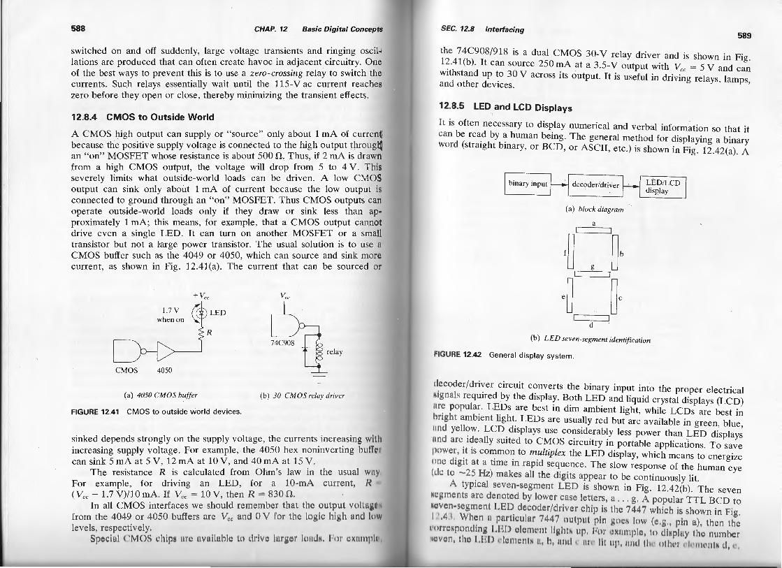
12.8.4 CMOS to Outside World
A CMOS high output can supply or "source" only about 1 rnA of current because the positive supply voltage is connected to the high output through an "on" MOSFET whose resistance is about 500 !1. Thus, if 2 rnA is drawn from a high CMOS output, the voltage will drop from 5 to 4 V. This severely limits what outside-world loads can be driven. A low CMOS output can sink only about 1 rnA of current because the low output is connected to ground through an "on" MOSFET. Thus CMOS outputs can operate outside-world loads only if they draw or sink less than approximately 1 rnA; this means, for example, that a CMOS output cannot drive even a single LED. It can turn on another MOSFET or a small transistor but not a large power transistor. The usual solution is to use a CMOS buffer such as the 4049 or 4050, which can source and sink more current, as shown in Fig. 12.41(a). The current that can be sourced 0 1
l.7V when on
CMOS 4050
(a) 4050 CMOS buffer
LED
FIGURE 12.41 CMOS to outside world devices.
v ee
relay
(b) 30 CMOS relay driver
sinked depends strpngly on the supply voltage, the currents increasing with increasing supply voltage. For example, the 4050 hex noninverting bulll't can sink 5 rnA at 5 V, 12 rnA at 10 V, and 40 rnA at 15 V .
The resistance R is calculated from Ohm's law in the usual wu y For example, for driving an LED, for a 1 0-mA curre nt , I< (Vee -1.7V)/10mA. If Vee= 10V, then R = 830.0.
In all CMOS interfaces we should remember that the output voltu gt from the 4049 or 4050 buffers arc V,.,. nnd 0 V for th~ logic hi uh and Itt \\ leve ls, respectively.
Spn·inl C MOS vhips 111'1 ' IIVII ilahlv to dt ivc liii 'P,V t' htlldN. l•\11 l' XI t111pl1
SEC. 12.8 Interfacing 589
the 74C908/91 8 is a dual CMOS 30-V relay driver and is shown in Fig. L2.4 1(b). It can source 250 rnA at a 3.5-V output with Vee = 5 V and can withstand up to 30 V across its output. It is useful in driving relays, lamps, and other devices.
12.8.5 LED and LCD Displays
It is often necessary to display numerical and verbal information so that it can be read by a human being. The general method for displaying a binary word (straight binary, or BCD, or ASCII, etc.) is shown in Fig. 12.42(a). A
decoder/driver
(a) block diagram
a
~u . ub
,u u, d
(b) LED seven-segment identification
111GURE 12.42 General display system.
decoder/driver circuit converts the binary input into the proper electrical ig nals required by the display. Both LED and liquid crystal displays (LCD) u·c popular. LEDs are best in dim ambient light, while LCDs are best in brig ht ambient light. LEDs are usually red but are available in green, blue, tud ye llow. LCD displays use considerably less power than LED displays 111cl are ideally suited to CMOS circuitry in portable applications. To save power, it is common to multiplex the LED display, which means to energize OIIC digit a t a time in rapid sequence. The slow response of the human eye (d l' to - 25 Hz) makes all the digits appear to be continuously lit.
I\ typical seve n-segment LE D is shown in Fig. l2.42(b). The seven 1 ' / '. m~.: nt s arc denoted by lower case le tt e rs, a . .. g. I\ popular TTL BCD to I'Vl' ll· scg mc ul L EI) <kcodc r/driv ~.: r chip is lhc 74117 which is shown in Fig. I
1,.'11, When ll p:u·tin ll nr 7,1,1? o ulpul pi11 goes low (e .g., pin n) , then the
II II H'Spo ndin/'. I, Jo; () cknt l' tlf l i/ •.lti N up J•'tll I '~ II IIIJII t • , l o tl isplny lilt• 1111111l wr I' VI ' II , lht• LJ.: J) I' II ' II H' III N II , h, ll lld I 1111 ' Ill lip , ll ild Il l! • l tlli t•t I ' II ' IIH' III N d, 1',
590 CHAP. 12 Basic Digital Concepts
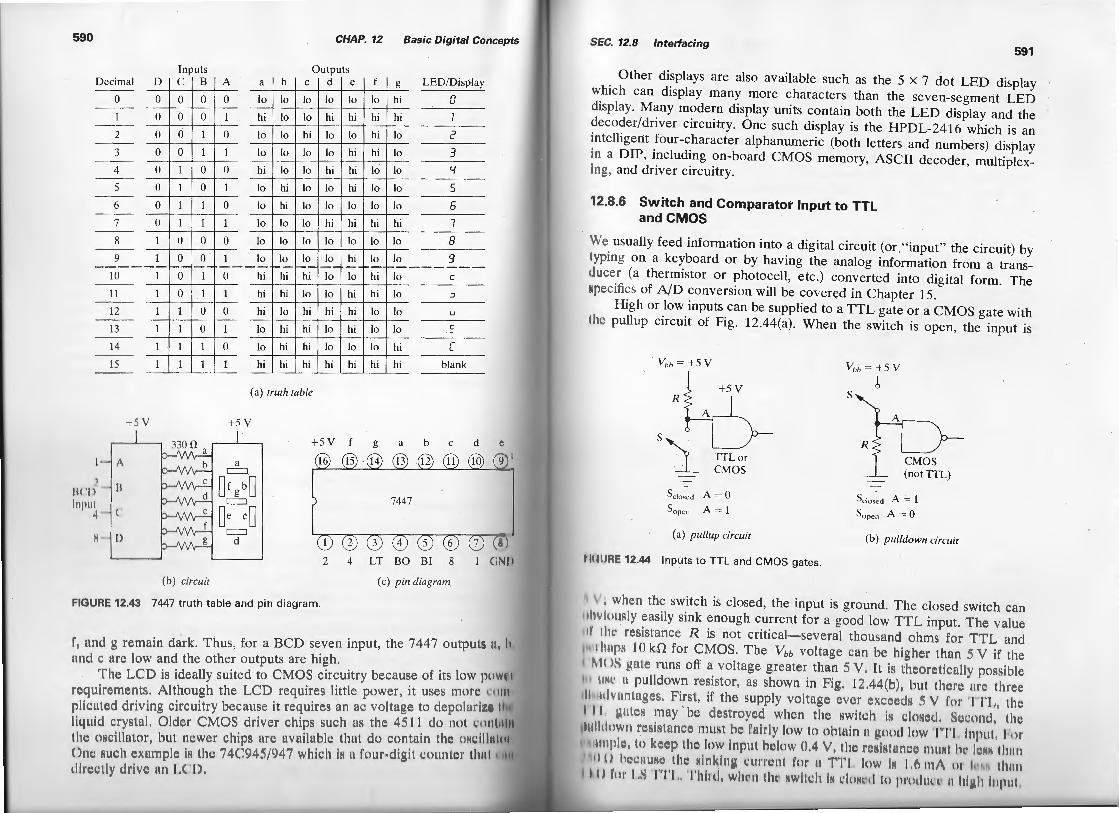
Inputs Outputs Decimal D c B A a b c d e f g LED/Display ---
0 0 0 0 0 lo lo lo lo lo to hi a -1 0 0 0 1 hi lo lo hi hi hi hi -2 0 0 1 0 lo lo hi lo lo hi lo 2 -3 0 0 1 1 lo lo lo lo hi hi lo 3 -4 0 1 0 0 hi lo lo hi hi lo lo '-1
---5 0 1 0 1 lo hi lo lo hi lo lo 5 -6 0 1 l 0 lo hi lo lo lo lo lo 5 -7 0 l l 1 lo lo lo hi hi hi hi 1 -8 1 0 0 0 lo lo lo lo lo to lo 8
- --9 1 0 0 1 lo lo lo 1o hi lo lo g
---------- -- -- ~- t--- -- - - --· 10 1 0 l 0 hi hi hi lo lo hi lo c -ll l 0 1 1 hi hi lo lo hi hi lo :J -12 l 1 0 0 hi lo hi hi hi to lo u -13 1 1 0 1 lo hi hi lo hi lo lo c -14 l 1 1 0 lo hi hi lo lo lo hi [ -15 I 1 l 1 hi hi hi hi hi hi hi blank
(a) truth table
I ) V +SV I
+SV f g a b c d c
i\ r ... hi I @ @ . @ @ (12) (1i) (fO) (9) I a =
lit 'I I I" ao~o lll pill t (' Oe cO H- 11 > I ...
v i = ( 0 Q) Q) 0 0 ® (j) ( t() d I
2 4 LT BO BI 8 I <:N i t
(b) circuit (c) pin diagram
FIGURE 12.43 7447 truth table and pin diagram.
f, 1111d g remain dark. Thus, for a BCD seven input, the 7447 output s 11 , l1 nml \..: a rc low and the other outputs are high .
The LCD is ideally suited to CMOS c ircuitry because o l' it s low IHI \\11 I'Wiui n;n•en l"s . Althoug h the LCD requires little power, it uses mol'e t'ltlll plk11t cd driving circui try because it requires an ac voltage to dcpolal'il'r th liquid nys ta l. O lde r C MOS driver c hips suc h as the 45 11 do not 1'11111 11111 tl w os<:i llator, hut newer l: hip:-; an; av ailahk that do co ntain th~· ost lil lllltt ( h!l' HIH'h \' XI IIIIJ)k iN tht~ 7tJ.( '()ll 5/ 1)47 Whirh is II fOIIf •digi t t'O llllt l' l' I hill 1111 dil ~ ~ ~ · tt y driVl' 11 11 1,( ' I) ,
SEC. 12.8 Interfacing 591
Other displays are also available such as the 5 x 7 dot LED display which can display many more characters than the seven-segment LED display. Many modern display units contain both the LED display and the ' decoder/driver circuitry. One such display is the HPDL-2416 which is an intelligent four-character alphanumeric (both letters and numbers) display in a DIP, including on-board CMOS memory, ASCII decoder, multiplexing, and driver circuitry.
12.8.6 Switch and Comparator Input to TTL and CMOS
We usually feed information into a digital circuit (or ."input" the circuit) by lyping on a keyboard or by having the analog information from a transducer (a thermistor or photocell, etc.) converted into digital form. The kpecifics of A/D conversion will be covered in Chapter 15.
High or low inputs can be supplied to a TTL gate or a CMOS gate with Ill ~; pullup circuit of Fig. 12.44(a). When the switch is open, the input is '
VJ,i> = +5 v
R
TTL or CMOS
Sclo,ed A= 0
Sopen A= 1
(a) pullup circuit
IIIIJIIE 12.44 Inputs to TTL and CMOS gates.
vhh = +5 v
s !
Sclosed A = 1
Sopen A= 0
(b) pulldown circuit
\ • when the switch is closed, the input is ground. The closed switch can '"'' lously easily sink enough current for a good low TTL input. The value •I IIH• •·e:-;istance R is not critical-severa l thousand o hms for TTL ;md
I" ll utps I 0 kf! for C MOS. The Vvv voltage can he hig her than 5 V it' the ' ~II IS ga le runs oft· a voltage greater than 5 V . It is thcorcliL·all y pos~ibl c i .. IHH· 11 pu lldown res isto r, as shown in Fig. 12.44(1>), hul tlu.••t• III'L' tlucc II tdV!I nlng~;s. l' irst., if the supply voltag~.: ever exl.'l't)dN 51 V 1'111 '1"1'1., ll~t• I II g 11t~·s nwy · hu tlus lroycd when thu sw iteh is l'IWHid , Sl ll'o nd , thv
11dldow11 tys isiHIICL' lllltNt lw l':~il'ly low to o btain :1 good low '1"1'1 lnpttl l •'o • llllplt o, to kl'l'P tlw low inpu t hdow 0.• 1 V, till' ll 'NiH llltH't• IIIIIHI lu• lt'Nil ll llltl Ill/ l't'l' II II Sl' thv tl i nk ln~t t' lllll ' ttl 1'111 11 '1''1'1 , ln w IN I It 111 /\ "' li NN 11 11 111
I II l111 I .S '1''1'1.. 'l 'hlitl , wltt•o tlu• NWlit•lt Ill rlorH•d 1!1 Jlllliltll t • II llt11li itlpt il ,
592 CHAP. 12 Basic Digital Concepts
a large current is drawn from the supply: I = 5 V /250 n = 20 rnA. This pulldown circuit should be avoided for TTL inputs, but it can be used for CMOS. R can be much larger than 250 0 in CMOS circuits.
Finally, mechanical switches are almost never used to supply high and low logic inputs to digitar gates because they "bounce" open and shut (fot approximately 10 ms) when they are closed. The remedy is the "bounce less" switch, described in Section 12.8:7.
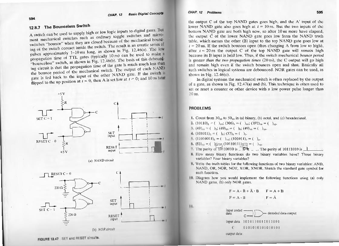
A comparator can drive a T1'L circuit, as shown in Fig. 12.45(a). Tlw
+SV +SV +SV +15 V +Vee +Vee
TTL CMOS
(a) open collector comparator to TTL (b) open collector comparator to CMOS
+SV
+lSV+SV
- lSV
(c) bipolar output from comparator (d) transistor drive
FIGURE 12.45 Comparator/TTL-CMOS interfacing.
output of many comparators is of the open collector type, so a pullup resistor is used to +5 V for driving TTL and to Vee for CMOS. In l•tp 12.45(b) the resistance R' is necessary to limit the current through lh CMOS protection diodes. The circuits of Fig. 12.45(a) and (b) are suilnltl for a comparator that runs between a positive supply voltage and gr01111tl because then the high comparator output provides a suitable '1''1'1 ttl
CMOS high, and a low comparator output is essentially at ground , whh h provides a good low for both TTL and CMOS. But if a bipolar or ( 'Me I
op amp is used as a comparator, its output can swing from + 13 V to I 1•, high to -13 V to - 15 V low, and the low output can destroy th<.: T ' I'L p11t input c ircuitry . A protective diod t.: with a 100-H c urr~; nt - lillliting H·H h.ltt
I Sl.lL~ Fig . 12 .11 <:; (!')I lli'I'YI'II IH I he low front p,oinp, lwlow ltppm xh nttld
'EC. 12.8 Interfacing 593
0.6 V. At this writing most experimentalists use comparators that swing lrom a positive voltage to near ground, so this is not a real problem. Another way of driving TTL is to use the comparator output to turn on an 11pn transistor, as shown in Fig. 12.45(d). A positive comparator output 111rns on Q and thus provides a low input of 0.2 V to the TTL gate. A tti'gative comparator output turns Q off and provides a high TTL input of I V. Thus the transistor acts as an inverter. The protective diode is
tH•cessary to prevent the negative comparator output from exceeding the tl ll tximum base emitter breakdown voltage (typically 7 V) of Q. The resislll nce R limits the base drive to Q.
For example, for a good low, Q should be saturated and its collector \ 11ltage will be 0.2 V. Thus, 11 = (5 V- 0.2 V)/3 kfi = 1.6 rnA, and 1
2 =
I flmA for the low sinking current for a good TTL low. Thus, Ic = 3.2 rnA, It ttl the base current is IB =lei hFE = 3.2 mA/100 = 32 p.A. When Q is 111 u rated, its base voltage will be approximately 0. 7 V and thus R =
il l V- 0.7 V)/0.032 rnA= 384 kfi. This is a maximum value for R. To 1 II'Hne saturation of Q, we would use a smaller value for R.
15 v
1 kf!
1< 5 VA~ .> ~5
s\ I s,,o]Wo m< I
+5V-
(11) bouncing mechanical switch (b) NAND debounced switch
+ 5 v
( V) Nl If< rll'illllllll 'l'ti ,1' 11 •/11'/r
111111111 1~ .411 IIIIIIII IICih iiHI IIWIII "
CHAP. 12 Basic Digital Concep 594
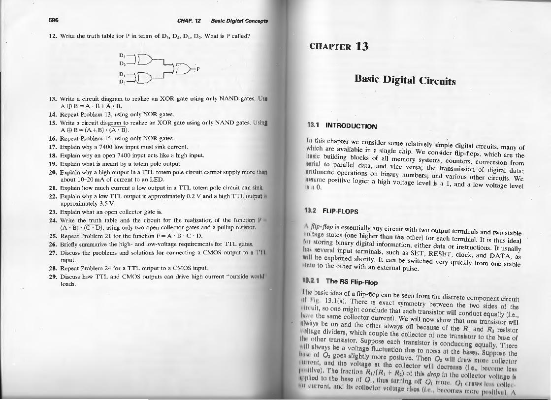
12.8.7 The Bounceless Switch A switch can be used to supply high or low logic inputs to digital gates. Bul most mechanical switches such as ordinary toggle switches and micro switches "bounce" when they are closed because of the mechanical boum· ing of the switch contact inside the switch. The result is an erratic series ol pulses approximately 1-10 ms long, as shown in Fig. 12.46(a). The low propagation time of TTL gates (typically 10 ns) can be used to make u "bounceless" switch, as shown in Fig. 12.46(b). The basis of this deboum ing circuit is that the propagation time of the gate is much mu~h less th1111 the bounce period of the mechanical switch. The output of each NANil gate is fed back to the input of the other NAND .gate. If the switch i flipped to the up position at t = 0, then A is set low at t = 0; and 10 ns lai r I
+SV
-u SET C = 1
-u RESETC = 0
R
+SV
___fL_!ESET C = 0
_n_. SET C = 1
c c1 I I . , I I I I
1 : : I I I I
SET I ----~~~-----input I \ : _,..
1 I
RESET 1 r-
t
I
input I I..,..,
(a) NAND circuit
c c 1 I 1
I I
SET input
I I I I I I I I I I I
I I
I I I
RESET 0 input
(h) NO !< ci rcll i l
IAUI11l17..47 ~; 1 I tu11 llll li l I t:l l t: ll ltr.,
CHAP. 12 Problems 595
the output C of the top NAND gates goes high, and the A' input of the lower NAND gate also goes high at t = 10 ns. But the two inputs of the bottom NAND gate are both high now, so after 10 ns more have elapsed, I he output C of the lower NAND gate goes low from the NAND truth table, which means the other (B) input to the top NAND gate goes low at 1 = 20 ns. If the switch bounces open (thus changing A from low to high), 11fter t = 20 ns the output C of the top NAND gate will remain high because its B input is held low. Thus, if the switch mechanical bounce period Is greater than the two propagation times (20 ns), the C output will go high und remain high even if the switch bounces open and shut. Basically all Nt1ch switches in logical systems are debounced. NOR gates can be used, as 11 hown in Fig. 12.46(c).
In digital systems the mechanical switch is often replaced by the output nf a gate, as shown in Fig. 12.47(a) and (b) . This technique is often used to
t• l or reset a counter or other device with a low power pulse longer than 10 ns.
l'hOBLEMS
I . Count from 3010 to 5010 in (a) binary, (b) octal, and (c) hexadecimal.
. ( I 0110)2 = ( ) 10 ; (306)s = ( )10; (3F2) 16 = ( )10•
I, (11-9)10 = ( )2; (49)Io = ( )s; (49)10 = ( ),o.
I. (I 0101 1)2 = ( )8 ; (37)s = ( ) 2.
, ( 11010011)2 = ( )1 6 ; (101011)2 = ( )s.
h , (63) ,0 = ( )F (10110111~ = ( ) 10•
• The parity of--icf110010 is -~ . The parity of 10111010 is ___:!., __ _
II , I low many binary functions do two binary variables have? Three binary variables? Four binary variables?
'' Write the truth tables for the following functions of two binary variables: AND, NAND, OR, NOR, NOT, XOR, XNOR. Sketch the standard gate symbol for 1111rh !'unction.
Ill I ll11g ram how you would implement the following functions using (a) only NA ND gates, (b) only NOR gates.
F=A ·B+A·B
F = A ·B
F=A+B
F=A
input coded ~D-datu ('-/ decoded data output
lnpul dat u I() I 0 I 1110 I I (I I I 00 I
( ' 0 I il l () I ll I ll I ill 0 Iii I
iiiii J' IIIII ttlll
596 CHAP. 12 Basic Digital Concepts
12. Write the truth table for Pin terms of D3 , D 2 , Dt. D0 • What is P called?
~:::::)D--.___, D-• Dl=:),~ 02
13. Write a circuit diagram to realize an XOR gate using only NAND gates. Us1· A EBB =A· B +A ·B.
14. Repeat Problem 13, using only NOR gates.
15. Write a circuit diagram to realize an XOR gate using only NAND gates. Usiul' A EBB= (A +.B)· (A· B).
16. Repeat Problem 15, using only NOR gates.
17. Explain why a 7 400 low input must sink current.
18. Explain why an open 7400 input acts like a high input.
19. Explain what is meant by a totem pole output.
20. Explain why a high output in a TTL totem pole circuit cannot supply more th 1111 about 10-20 rnA of current to an LED.
21. Explain how much current a low output in a TTL totem pole circuit can siuk
22. Explain why a low TTL output is approximately 0.2 V and a high TTL output approximately 3.5 V.
23. Explain what an open collector gate is.
24. Write the truth table and the circuit for the realization of the function I (A ·B) · (C ·D), using only two open collector gates and a pullup resisto l" .
25. Repeat Problem 21 for the function F =A · B · C · D. 26. Briefly summarize the high- and low-voltage requirements for TTL gates.
27. Discuss the problems and solutions for connecting a CMOS output to 11 ' I II input.
28. Repeat Problem 24 for a TTL outputto a CMOS input.
29. Discuss how TTL and CMOS outputs can drive high current " outside w" ''" loads .
CHAPTER 13
Basic Digital Circuits
13.1 INTRODUCTION
111 1 his chapter we consider some relatively simple digital circuits, many of wllich are available in a single chip. We consider flip-flops, which are the lu•sic building blocks of all memory systems, counters, conversion from "''da l to parallel data, and vice versa; the transmission of digital data; ulf hmetic operations on binary numbers; and various other circuits. We
IIIH-Hi me positive logic: a high voltage level is a 1, and a low voltage level I 0.
I 1.2 FLIP-FLOPS
\ {li{l - flop is essentially any circuit with two output terminals and two stable 1
11Hnge states (one higher than the other) for each terminal. It is thus ideal 1111 Hlori ng binary digital information, either data or instructions. It usually li uN several input terminals, such as SET, RESET, clock, and DATA, as uill he explained shortly. It can be switched very quickly from one stable fuft • lo the other with an external pulse.
.1 The RS Flip-Flop
II II ' husic idea of a flip-flop can be seen from the discrete component circuit oil l •'lp, . 13.l(a). There is exact symmetry between the two sides o f lhe ' Ito 1111 , so o ne mig ht conclude that each transistor will co nduct equally (i.e., li tl\'1' I he same collector current). We will now show fhal on<.: ln~ns i s l or will tl wllyN be o n and the other always off because of fhc U1 and f<_, ros islo r nll11p, ~· d ivide rs, which couple the collec lor of o ne fransislor lo lhl' hHHC of
tlu ot he r· lnmsislor. Suppose eac h frans islor is ro nducting tlqt~rtll y . 'l' h l' l\'
II ulwnys l'>e a vollagc lhrc luulio n due lo noise nl the hrtNt·s. S11ppllNl' fh ~· iltlol of ()~ gOes slig iJIIy IIIOI'C posili vl.: . 'J'IJl' ll ()_, wi ll di'IIW 111011' 1'11 111'1 for
111 11'111 , 11 11d flu.J volln g~· 111 fh t- co lloc lor wil l dtH' I'l ' II Ni' (1.• •., lu•tt llll l' ~~ ~ I 'll if lvt') , Till' 1'1111'fio11 1< 1/(1< 1 I U ,) nf I his rll'llfl l11 I Itt • l'lt ll t'l In• vn lfllp, " l1 lj l)l lh•d In llw IHINO ol' O, , fhii N fllrll l iiH oil' ( )
1 111111 o U
1 ti1 11Wil ln11N 1c•ll •1
1•11 I 111 11 ' 111 , ll lld li N I IIIII I tor Vllltll/'.1' I INON (lt •' lu lllllll lH '"'"' p<!Mitll•t) r\