Embed Size (px)
Citation preview
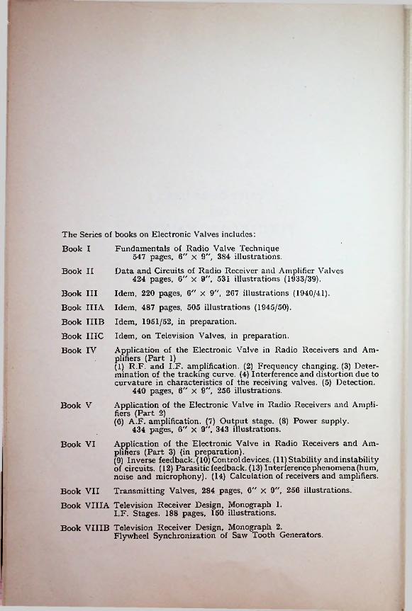
The Series of books on Electronic Valves includes:
Fundamentals of Radio Valve Technique 547 pages, 6" X 9", 3S4 illustrations.
Book II Data and Circuits of Radio Receiver and Amplifier Valves 424 pages, 6" X 9". 531 illustrations (1933/39).
Book III Idem, 220 pages, 6" x 9", 267 illustrations (1940/41).
Book III A Idem, 487 pages, 505 illustrations (1945/50).Book IIIB Idem, 1951/52, in preparation.
Book IIIC Idem, on Television Valves, in preparation.Book IV Application of the Electronic Valve in Radio Receivers and Am
plifiers (Part 1)(1) R.F. and I.F. amplification. (2) Frequency changing. (3) Determination of the tracking curve. (4) Interference and distortion due to curvature in characteristics of the receiving valves. (5) Detection.
440 pages, 6" X 9", 256 illustrations.Book V Application of the Electronic Valve in Radio Receivers and Ampli
fiers (Part 2)(6) A.F. amplification. (7) Output stage. (8) Power supply.
434 pages, 6" x 9", 343 illustrations.
Book VI Application of the Electronic Valve in Radio Receivers and Amplifiers (Part 3) (in preparation).(9) Inverse feedback. (10) Control devices. (11) Stability and instability of circuits. (12) Parasitic feedback. (13) Interference phenomena (hum, noise and microphony). (14) Calculation of receivers and amplifiers.
Book VII Transmitting Valves, 284 pages, 6" X 9", 256 illustrations.
Book VIIIA Television Receiver Design, Monograph 1.I.F. Stages. 188 pages, 150 illustrations.
Book VIIIB Television Receiver Design, Monograph 2.Flywheel Synchronization of Saw Tooth Generators.
Book I
BOOK VIII A
TELEVISION RECEIVER DESIGN
I. F. STAGES

TELEVISION RECEIVER
DESIGNMonograph 1
I. F. STAGESU.D.C. 621.397.62
byA. G. W. U I T J E N S
BibliothcekCent rani La bora tor ium F I
St. Paul ••>>* mat 4 I /c'idschuidam
1953
PHILIPS’ TECHNICAL LIBRARY
rights reserved by N.V. Philips' Gloeilampcnfabrickcn Nv Eindhoven (Holland)
in this book arc given without prejudice
o patent rights of the above company
First published 1953 Printed in the Netherlands
FOREWORD
Parts IV, V and VI *) of this series of books deal with all those problems which relate to the application of the electronic valve in radio receivers and amplifiers. As explained in their prefaces, the material has been based mainly on Philips’ publications, but the articles have been arranged in a logical sequence and, where necessary, revised and supplemented so as to bring the subject matter up to date.
In this manner a work has been compiled which, as a guide and source of information, is indispensable to set-makers and at the same time is greatly valued as material for practical study in secondary and higher technical training institutions.
It was, therefore, not surprising that suggestions have been received from various quarters that a similar work on the problems encountered in the design and construction of television receivers should be published. Although the technique of television reception is still in its infancy and has by no means reached a stabilized state, it has been decided to publish such a work under the title of Television Receiver Design, but in a slightly different format. In the work on radio receivers, chapters dealing with the many different aspects of the subject are printed in three bound volumes, but Television Receiver Design will comprise a series of 6 to 8 parts, each dealing with a specific aspect of television receiver design, and the whole forming a complete and comprehensive treatise.
The first part, entitled F. Stages”, deals with the application of the pentode in the intermediate frequency section of a superheterodyne receiver and the high frequency stages of a T.R.F. receiver. The second part, now at press, treats of flywheel circuits and synchronization. Other parts will cover such subjects as deflection circuits, problems related to the high-frequency stages, etc.
It is hoped that this work will prove to be just as valuable in its particular sphere as are the series of books on the construction of radio receivers.
J. HAANTJESPHILIPS ELECTRONIC TUBE DIVISION
* Part VI is now in course of preparation.
PREFACE
This monograph deals particularly with pentode amplifiers operating in a frequency range lying roughly between 10 Mc/s and over 100 Mc/s. The high-frequency amplifiers of T.R.F. receivers (40 Mc/s to 70 Mc/s) also come under this definition, and thus, while not strictly coming •within the scope of this book, have had to be included for the sake of completeness. On the other hand, the choice of the intermediate frequency has not been touched upon because this is so closely related to the problem of high-frequency amplification and frequency changing that it is considered better to deal with this subject in a separate book.
In order that the exposition may be quite clear to the reader, it has been necessary to use in some parts of the text formulae which do not directly follow from the preceding comments. The derivations of these formulae are to be found in the appendices at.the end of the book.
Finally, a word of recognition is to be added, not only for the use that has been made of the literature quoted, but also for the support given by many colleagues, among whom I am particularly indebted to Jhr. Ir. H. van Suchtelen for many discussions and valuable advice, to Mr. H. Kater for editing the manuscript and to Mr. Harley Carter A.M.I.E.E. of Mullard Ltd., London, who scrutinized the manuscript.
\\
The Author
Eindhoven, October 1952.
!
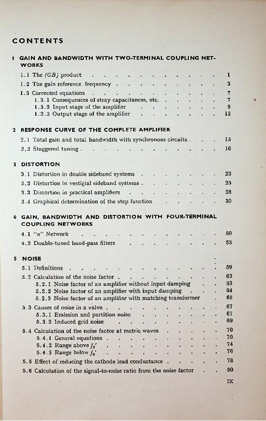
CONTENTS
1 GAIN AND BANDWIDTH WITH TWO-TERMINAL COUPLING NETWORKS
1.1 The (GB) product..................................................................................1.2 The gain reference frequency..................................................................1.3 Corrected equations..................................................................................
1.3.1 Consequences of stray capacitances, etc......................................1.3.2 Input stage of the amplifier.................................................1.3.3 Output stage of the amplifier.................................................
13
77 9
812
2 RESPONSE CURVE OF THE COMPLETE AMPLIFIER
2.1 Total gain and total bandwidth with synchronous circuits .2.2 Staggered tuning..........................................................................
1516
3 DISTORTION
3.1 Distortion in double sideband systems .3.2 Distortion in vestigial sideband systems .3.3 Distortion in practical amplifiers3.4 Graphical determination of the step function
23
2528
30
4 GAIN, BANDWIDTH AND DISTORTION WITH FOUR-TERMINAL COUPLING NETWORKS
4.1 "tt” Network...........................................................................................4.2 Double-tuned band-pass filters..........................................................
5053
5 NOISE
5.1 Definitions...........................................................................................5.2 Calculation of the noise factor..........................................................
5.2.1 Noise factor of an amplifier without input damping5.2.2 Noise factor of an amplifier with input damping5.2.3 Noise factor of an amplifier with matching transformer
5.3 Causes of noise in a valve..................................................................5.3.1 Emission and partition noise.........................................5.3.2 Induced grid noise..........................................................
5.4 Calculation of the noise factor at metric waves ....5.4.1 General equations..................................................................5.4.2 Range above /„'..................................................................5.4.3 Range below /„'..................................................................
5.5 Effect of reducing the cathode lead conductance ....5.6 Calculation of the signal-to-noise ratio from the noise factor
5963636465676769707074767880
IX
6 FEEDBACK
6.1 General...........................................................................................6.2 Basic formulae...................................................................................6.3 Feedback from anode to grid..........................................................
6.3.1 Negative feedback by a resistance.................................6.3.2 Feedback by the anode-to-grid capacitance6.3.3 Maximum permissible values of p-.................................6.3.4 Staggered tuning..................................................................6.3.5 Maximum permissible gain..................................................6.3.6 Coupling by means of band-pass filters (I.F. transformers)6.3.7 Deviations at higher frequencies.................................
6.4 Feedback by the cathode-to-grid admittance ....6.4.1 Self-inductance in the cathode lead.................................6.4.2 Reducing the conductance by means of a cathode capacitor6.4.3 Small resistor in the cathode lead.................................6.4.4 Stabilization of the input admittance ....6.4.5 Valves with double cathode connection ....
6.5 Feedback by the anode-to-cathode capacitance ....6.6 Other forms of feedback...................................................................
838486868892959798
102103104106108110112113114
7 PRACTICAL CONSIDERATIONS FOLLOWING ON THE THEORY
7.1 Sensitivity........................................................................................... 1161167.2 Gain
7.2.1 Gain of the input circuit7.2.2 Gain of the I.F. amplifier
1171171197.3 Selection of the valves
7.4 Staggered tuning systemAPPENDIX I APPENDIX II . .APPENDIX III ... APPENDIX IV .APPENDIX V . ...TABLE 1 .................................TABLE 2.................................TABLES 3 and 4 LIST OF SYMBOLS
. 122134152154163166168170172173
X
:
1 GAIN AND BANDWIDTH WITH TWO-TERMINAL COUPLING NETWORKS
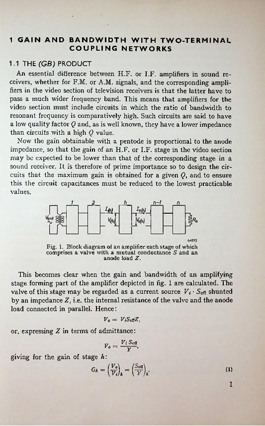
1.1 THE (GB) PRODUCTAn essential difference between H.F. or I.F. amplifiers in sound re
ceivers, whether for F.M. or A.M. signals, and the corresponding amplifiers in the video section of television receivers is that the latter have to pass a much wider frequency band. This means that amplifiers for the video section must include circuits in which the ratio of bandwidth to resonant frequency is comparatively high. Such circuits are said to have a low quality factor Q and, as is well known, they have a lower impedance than circuits with a high Q value.
Now the gain obtainable with a pentode is proportional to the anode impedance, so that the gain of an H.F. or I.F. stage in the video section may be expected to be lower than that of the corresponding stage in a sound receiver. It is therefore of prime importance so to design the circuits that the maximum gain is obtained for a given Q, and to ensure this the circuit capacitances must be reduced to the lowest practicable values.
JM
Fig. 1. Block diagram of an amplifier each stage of which comprises a valve with a mutual conductance S and an
anode load Z.
This becomes clear when the gain and bandwidth of an amplifying stage forming part of the amplifier depicted in fig. 1 are calculated. The valve of this stage may be regarded as a current source Vi • SCff shunted by an impedance Z, i.e. the internal resistance of the valve and the anode load connected in parallel. Hence:
Vo = ViSoaZ,
or, expressing Z in terms of admittance:Vi Sett
Y ’Vo =giving for the gain of stage h:
(1)Gh
1
1
Gain and bandwidth with two-terminal coupling networks 1
where Seff is the dynamic mutual conductance of the valve, which may be taken to be equal to the static mutual conductance provided the cathode impedance is zero. At the frequencies considered, transit time effects do not influence the mutual conductance to any appreciable extent.
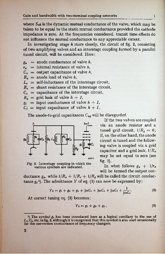
In investigating stage h more closely, the circuit of fig. 2, consisting of two amplifying valves and an interstage coupling formed by a parallel tuned circuit, will be considered. Here:
= anode conductance of valve h, ra = internal resistance of valve h,C0 = output capacitance of valve h,Ra = anode load of valve li,Lc = self-inductance of the interstage circuit,Rc = shunt resistance of the interstage circuit,Cc = capacitance of the interstage circuit,Rg = grid leak of valve h -f- 1,gi = input conductance of valve h -j- 1,Ci = input capacitance of valve h -j- 1,
ga
The anode-to-grid capacitances Cag will be disregarded.If the two valves are coupled
/)+/ via an anode resistor and aX" tuned grid circuit, l/Rg = 0; if, on the other hand, the anode circuit is tuned and the following valve is coupled via a grid capacitor and a grid leak, l/Ra may be set equal to zero (see fig. 2).
In what follows ga + l/ra will be termed the output con
ductance go, while 1 /Ra -j- 1 jRc + l/Rg will be called the circuit conductance gc1). The admittance Y of eq. (1) can now be expressed by:
fk^§ r==^a=rG>9a ' ~95r r648<?3
Fig. 2. Interstage coupling in which the various symbols are indicated.
1y?i = gi + go + gc + jcoCc + jcaC0 + jwCi +
At correct tuning eq. (2) becomes:
(2)jcoLe
(3)F* = gi + go + gc ,
x) The symbol gc has been introduced here as a logical corollary to the use of Lc, Cc, etc. in fig. 2, although it is recognized that this symbol is also used occasionally for the conversion conductance of frequency changers.
2
1.2 The gain reference frequency
while the gain G per stage is:ScaG = (4)
Si 4“ So 4“ Sc
Considering an amplifier with n identical stages and disregarding differences caused by different input and output circuits of the amplifier, the total gain Gtot is:
Y\Si + So + Sc)
Denoting by B the bandwidth within which the circuit impedance varies 3 db, the conductance of the intervalve circuit of valves h and h + 1 may be expressed by:
-Sett
Gtot (5)
S — Si 4" So 4" Sc — 2r.BC — 2tzB (Ci 4" Co 4“ Cc).(see Appendix la)
(6)
Substitution of this expression in eq. (4) gives:Seff (?)G- B =
2tz (Ci + Co 4" Gc)
This equation shows that the quantities which determine the gain and bandwidth are so related that a high gain can be obtained only at the cost of the bandwidth. The product G-B reaches the maximum when the circuit capacitance Cc (including the stray capacitances) is zero and when the dynamic mutual conductance Seff is equal to the static mutual conductance S. In that case this product is entirely determined by the valve characteristics and will be denoted as:
S(8){GB) =
2n (Ci + Co)
Eq. (8) shows that this (GB) product merely depends on the ratio of valve characteristics. If, for a given (GB) product, one of the quantities G or B is given, the maximum value of the other is fixed. It is, however, impossible to increase the gain G beyond a certain value by decreasing the bandwidth B. This is explained by eq. (3) in which the value of gi -f go + gc cannot be decreased indefinitely.
So long as gi -f- g0 is smaller than 2tcB(Ci + C0+ Cc) (cf. eq. (6)) the bandwidth can be adjusted to the desired value by suitable choice of gc until gc has reached the minimum value obtainable. Beyond this limit it is impossible to decrease B by decreasing gc. (For the present it will be assumed that it is possible to reduce gc to zero.)
1.2 THE GAIN REFERENCE FREQUENCY Another important difference between amplifiers for television and for
broadcast receivers is that the television signal frequencies (for both
3
Gain and bandwidth with two-terminal coupling networks 1
picture and sound) are very much higher than for normal broadcasting, being about 40 Mc/s to 200 Mc/s, and that intermediate frequencies in the order of 20 Mc/s to 50 Mc/s are employed.
At these high frequencies damping due to the valve conductances contributes largely to the total circuit damping. Now the input and output conductances of a valve, g* and g0, depend on the frequency which is to be amplified. The higher the frequency, the greater will be the damping, and the lower will be the maximum gain, until, at a certain frequency, the gain becomes unitj^, in other words the valve no longer amplifies. At still higher frequencies, the signal is even attenuated1). The frequency at which the maximum gain is unity is called the gain reference frequency (symbol fj.
It will be shown in Section 6 that the relationship between the conductances and frequency in the very-high frequency range (metric waves) is practically the same for all valves, and follows a square law, viz.:
gi + go = const, x /2.The magnitude of the constant in this expression depends on the valve characteristics and differs for each type of valve.
This implies that the maximum gain which can be obtained with a given valve is determined by the frequency and by a valve constant, for if gc is put equal to zero to obtain the maximum gain, then, according to eqs (1) and (3), the gain is determined by the dynamic mutual conductance SCft and g* + g0. The maximum value of SCff is equal to the static mutual conductance 5. Since at the frequencies under consideration there is little difference between the dynamic and static mutual conductances provided no additional impedances are included in the cathode lead, the maximum gain may be expressed by:
Gmax = const. X f~2.At the gain reference frequency the maximum gain G
that this expression may also be written as:
(9)
= 1, SOmax
-W (10)Gmax
The possibilities of an amplifier can now be investigated more closely. In practice the design of the amplifier is always based on the required bandwidth B0. It is obvious that this governs the gain obtainable, G0, and the required value of g; + g0 + gc- Considering the possibilities at in-
*) M. J. O. Strutt, Gain and Noise Figures at V.H.F. and U.H.F., Wireless Eng. XXV, p. 21, 1948 (No. 292).4
1.2 The gain reference frequency
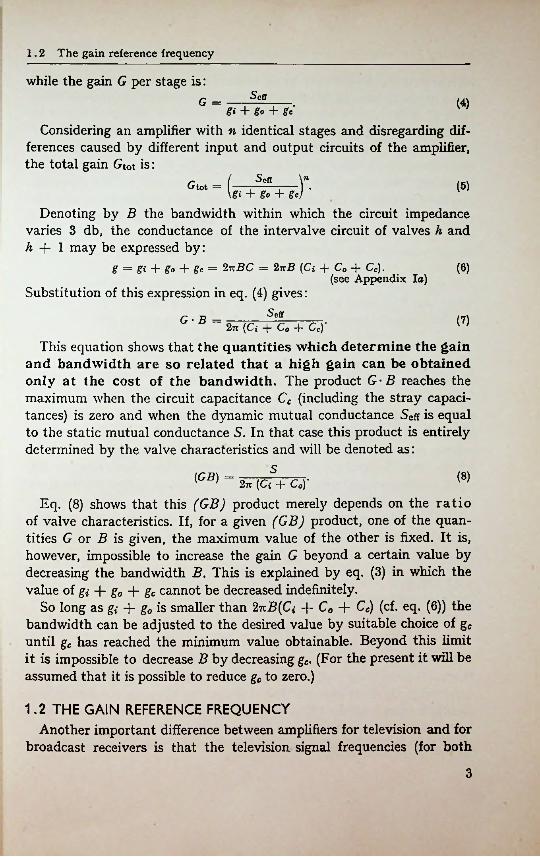
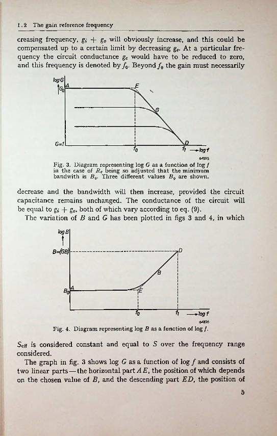
creasing frequency, gi + g0 will obviously increase, and this could be compensated up to a certain limit b}' decreasing gc. At a particular frequency the circuit conductance gc would have to be reduced to zero, and this frequency is denoted by /0. Beyond /0 the gain must necessarily
logGE
n6=1fo fl —+1ogf
6<895Fig. 3. Diagram representing log G as a function of log / in the case of Rc being so adjusted that the minimum bandwith is B0. Three different values B0 are shown.
decrease and the bandwidth will then increase, provided the circuit capacitance remains unchanged. The conductance of the circuit will be equal to gi + g0, both of which vary according to eq. (9).
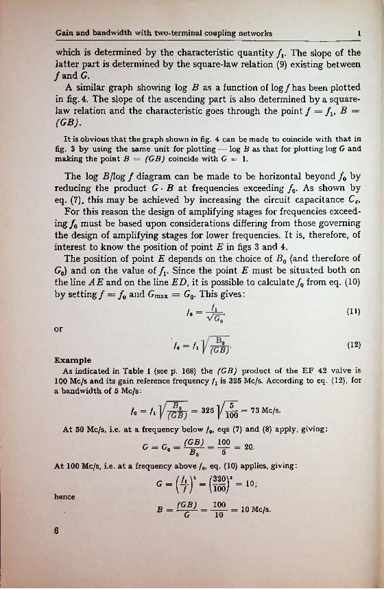
The variation of B and G has been plotted in figs 3 and 4, in which
logB
Ib=(gb)
fi —+logf64896
Fig. 4. Diagram representing log B as a function of log /.
fo
Soft is considered constant and equal to S over the frequency range considered.
The graph in fig. 3 shows log G as a function of log / and consists of two linear parts — the horizontal part AE, the position of which depends on the chosen value of B, and the descending part ED, the position of
5
Gain and bandwidth with two-terminal coupling networks 1
which is determined by the characteristic quantity fv The slope of the latter part is determined by the square-law relation (9) existing between / and G.
A similar graph showing log B as a function of log / has been plotted in fig. 4. The slope of the ascending part is also determined by a square- law relation and the characteristic goes through the point / = fv B =(GB).
It is obvious that the graph shown in fig. 4 can be made to coincide with that in fig. 3 by using the same unit for plotting — log B as that for plotting log G and making the point B = (GB) coincide with G = 1.
The log 5/log / diagram can be made to be horizontal beyond f0 by reducing the product G • B at frequencies exceeding /0. As shown by eq. (7), this may be achieved by increasing the circuit capacitance Cc.
For this reason the design of amplifying stages for frequencies exceeding /0 must be based upon considerations differing from those governing the design of amplifying stages for lower frequencies. It is, therefore, of interest to know the position of point E in figs 3 and 4.
The position of point E depends on the choice of B0 (and therefore of G0) and on the value of fv Since the point E must be situated both on the line AE and on the line ED, it is possible to calculate f0 from eq. (10) by setting f — f0 and Gmax = G0. This gives:
(11)/o —
or
(12)/o — /1Example
As indicated in Table 1 (see p. 168) the (GB) product of the EF 42 valve is 100 Mc/s and its gain reference frequency fx is 325 Mc/s. According to eq. (12), for a bandwidth of 5 Mc/s:
1Y ioo 73 Mc/s./o — fi = 325
At 50 Mc/s, i.e. at a frequency below /„, eqs (7) and (8) apply, giving:^-155 = 20.
At 100 Mc/s, i.e. at a frequency above /0, eq. (10) applies, giving:
G = G0 =B0
hence(GB) 100— = 10 Mc/s.B = G
6
1.3 Corrected equations 1.3.1
1.3 CORRECTED EQUATIONSThis simple method of calculation has been made possible only by a
very idealized representation of the amplifier and it is now necessary to investigate what corrections are required to render the results more accurate and to extend their validity.
The two simplifications made in the preceding calculations were:(1) It was assumed that the total circuit capacitance is equal to C* -f- C0
and that the dynamic mutual conductance Seff is equal to the static mutual conductance S.
(2) The calculations were based on the assumption that the amplifying stage is preceded and followed by an identical stage.
1.3.1 Consequences of stray capacitances, etc.The extent to which it is permissible to ignore the circuit capacitances
Cc will first be investigated.In broadcast receivers the choice of the circuit capacitance Cc is often
determined by the desire to obtain a high value of Q\ but, as explained above, a high Q is not possible in T.V. receivers. In a receiver containing circuits with a high Q value tuning must be very accurate because a small relative detuning corresponds to a large proportion of the bandwidth. A small fractional shift of the resonant frequency of one of the circuits therefore results in quite a considerable modification of the response curve.
Now the valve capacitances are not entirely constant (for example the variation AC; in the case of gain control being applied, see also Section 6), and it is therefore desirable to minimize the effect of these variations by ensuring that the valve capacitances are small compared with the total circuit capacitance.
This argument does no apply in T.V. receivers in view of the very low quality factors of the circuits. It is nevertheless desirable to keep these variations within reasonable limits; the circuit capacitance can then be reduced to the minimum. This is advantageous because the gain at a given bandwidth can then be increased to its maximum value.
It is of course not practicable to reduce the total circuit capacitance to C; + C0, owing to the existence of unavoidable stray capacitances of the wiring, the coils, etc. and “electronic” capacitance of the valve. These stray capacitances are represented by an additional term Cx, which is added to the circuit capacitance.
It is, therefore, no longer permissible to replace G • B simply by the
7
Gain and bandwidth with two-terminal coupling networks 1
(GB) product, but it should be written:G • B = Fx (GB), (13)
in whichCj -j- Co
Ci + Co + CxThis becomes obvious when eq. (7), in which Cc is put equal to Cx, is
compared with eq. (8). It is moreover seen that in eq. (8) the term S occurs instead of the term SCfi in eq. (7). To remove this discrepancy, eq. (13) will be rewritten as:
(14)Fx =
(13a)G • B = FSFX (GB),in which
Seff (15)Fs = S 'If, for example, a non-bypassed cathode resistor Rk is used, then:
lFs = 1 + Sk Rk’
where Sk denotes the cathode transconductance <?/*/<? 7g.Not only is it necessary to revise the calculation of G • B as shown
above, but that of Gmax must also be corrected. Eq. (10) for this quantity includes only terms depending on the mutual conductance and no term related to the circuit capacitances. The corrected equation, therefore, contains no term Fx and becomes:
Gmax — F$ j • (10a)
The calculation of /0 can now easily be corrected, eqs (11) and (12) becoming:
(lla)/o — /iand
/o - /l]/ *0(12a)Fx• (GB)'
1.3.2 Input stage of the amplifierThe assumption that an identical stage precedes the stage of which the
gain is to be calculated does not hold for the first stage of the amplifier, and the necessary correction for this stage will now be investigated for the case of a “straight” (T.R.F.) receiver.
The gain of the first valve, between control grid and anode, can be calculated as before. The valve is, however, preceded by a transformer for matching the input impedance of the amplifier to the aerial. Correct matching is particularly important in T.V. receivers in order to avoid
8
1.3 Corrected equations 1.3.2
reflections in the aerial cable, the effects of which are commonly termed “ghosts”.
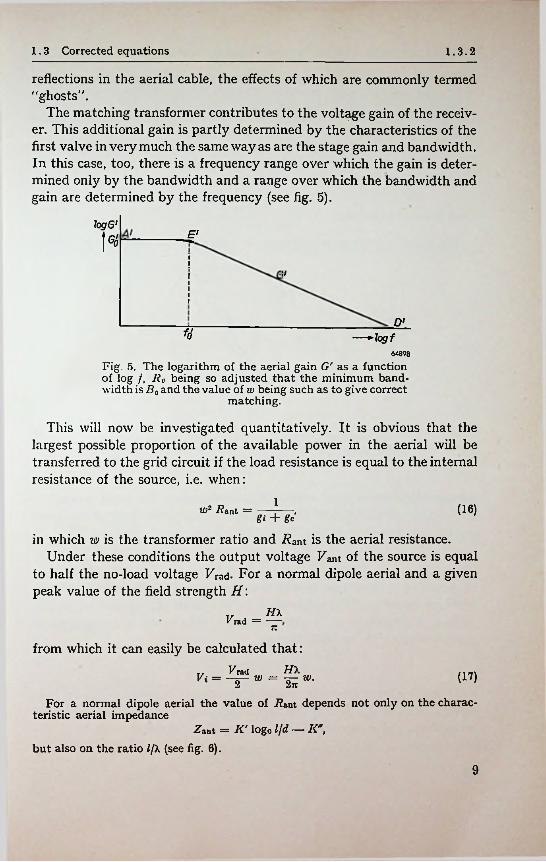
The matching transformer contributes to the voltage gain of the receiver. This additional gain is partly determined by the characteristics of the first valve in very much the same way as are the stage gain and bandwidth. In this case, too, there is a frequency range over which the gain is determined only by the bandwidth and a range over which the bandwidth and gain are determined by the frequency (see fig. 5).
logG'E'!<%'i
?/ii
D•—+logf
64898
Fig. 5. The logarithm of the aerial gain G' as a function of log f, Rc being so adjusted that the minimum bandwidth is Bq and the value of w being such as to give correct
matching.
This will now be investigated quantitatively. It is obvious that the largest possible proportion of the available power in the aerial will be transferred to the grid circuit if the load resistance is equal to the internal resistance of the source, i.e. when:
l (16)w- Runt = gi + go
in which w is the transformer ratio and .Rant is the aerial resistance.Under these conditions the output voltage Fant of the source is equal
to half the no-load voltage Frad. For a normal dipole aerial and a given peak value of the field strength H:
H\Fnui = —
7T
from which it can easily be calculated that:T. V:rad (17)
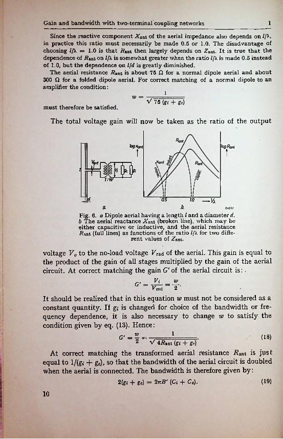
For a normal dipole aerial the value of Rant depends not only on the characteristic aerial impedance
Zant = K* loge l/d — li",
but also on the ratio l\\ (see fig. 6).9
Gain and bandwidth with two-terminal coupling networks 1
Since the reactive component .X’ant of the aerial impedance also depends on l/X, in practice this ratio must necessarily be made 0.5 or 1.0. The disadvantage of choosing l/X = 1.0 is that Rant then largely depends on Zant. It is true that the dependence of Rant on l/X is somewhat greater when the ratio lj\ is made 0.5 instead of 1.0, but the dependence on l/d is greatly diminished.
The aerial resistance .Rant is about 75 D for a normal dipole aerial and about 300 Q for a folded dipole aerial. For correct matching of a normal dipole to an amplifier the condition:
1
Vl5(gi + gc)must therefore be satisfied.
The total voltage gain will now be taken as the ratio of the output
logXani iogRasri
it
RIG Tj 1 Sfc 57
J—Jl
uw
d 0.5 1.0k3. 64857
Fig. 6. a Dipole aerial having a length l and a diameter d. b The aerial reactance Xant (broken line), which may be either capacitive or inductive, and the aerial resistance Rant (full lines) as functions of the ratio l/X for two diffe
rent values of Zant.
voltage V0 to the no-load voltage Vrad of the aerial. This gain is equal to the product of the gain of all stages multiplied by the gain of the aerial circuit. At correct matching the gain G' of the aerial circuit is: •
:i
Vi wG' ~ T/mcl 2 '
It should be realized that in this equation w must not be considered as a constant quantity. If gi is changed for choice of the bandwidth or frequency dependence, it is also necessary to change w to satisfy the condition given by eq. (13). Hence:
G' = -= .2 V 4Rant {gi + gr)
At correct matching the transformed aerial resistance .Rant is just equal to l/(gi + gc), so that the bandwidth of the aerial circuit is doubled when the aerial is connected. The bandwidth is therefore given by:
l (18)
(19)2(sri "b gc) — (Ci + Cx).
10
5
1.3 Corrected equations 1.3.2
It is now clear, for the input stage, that it is not the product G' • B butthe product G' • VB' which is constant. Eq. (13) of Section 1.3.1 now becomes :
G'Vb' = Fx (GB)' l) (136)in which
l 32.5(GBy = (7a)V 7?ant C» V Cl
andiV = ]/ C< (14a)Ci + Cx'
The maximum gain of the aerial circuit can be calculated by putting gc in eq. (18) equal to zero, which gives:
<V = 1V' 4 7?ant gi
where gt is again const, x /2, so that:c-fi Go - y
The position of the transitional point atis now given by:
(106)
fifo /• ^0(116)
orv'g.'
Fx'(GB)rfo = // (126)
ExampleA normal dipole aerial is tuned to exactly 60 Mc/s and correctly matched to the
input circuit preceding an EF 42 valve. The wiring capacitances are 3 pF. What is G' if B0' = 5 Mc/s?
According to Table 1 (p. 168), the gain reference frequency /1/ = 190 Mc/s and the figure of merit (GB)' = 10 (B in Mc/s).
Since Ci = 9.5 pF:
.1/«f; - y Cf = 0.87 .Ci -f- Cx 9.5 + 3From eq. (126):
fx' VB0' 190 V5 F/ (GB)' “ 0.87 x 10
Since / is higher than /0', eq. (106) applies:
~ fx 190 o «G = 7 = lo = 32>
« 50 Mc/s.fo =
x) Here it would in fact be more correct to write (G VB)' instead of (GB)'.
11
Gain and bandwidth with two-terminal coupling networks 1
giving, according to eq. (136):
0.87 X 10.5\2 = 5.8 Mc/s.D 3.8
According to whether the receiver operates at a frequency above or below /0 and /0', four cases arise:
(1) the frequency lies below both /0 and /</;(2) the frequency lies below /0 but above /0';(3) the frequency lies above both f0 and /0';(4) the frequency lies above /0 but below /0\
It will be seen later (Section 7) that in order to decide upon the most favourable design of the amplifier and input transformer it is of interest to know which of these cases applies.
T.R.F. receivers will usually be so designed that case (1) applies, but at higher frequencies (about 70 Mc/s) case (2) may occur. In superheterodynes, at the high T.V. band (about 200 Mc/s) case (2) always applies.
In view of the low gain per stage obtainable in case (3) this case will be avoided wherever possible. Case (4) does not occur in practice,/0 hardly ever being lower than /0'. This becomes obvious when /0 and /</ are calculated at B0 = B0'. From eqs (12a) and (126):
VFx/o A ' Fx (GB)' Fx' V2
It should be understood that the above considerations are based on the assumption that gc can always be made negligible with respect to gi + g0. In practice, however, the minimum value of gc may be quite considerable, especially in the aerial circuit. The implications of this in the above theory are dealt with in Section 7.
/o' A' VFz(GB) ■ yWr~co “•1/ 1gi + go vrgi
1.3.3 Output stage of the amplifierIn calculating the gain of the last valve of the amplifier it should be
borne in mind that this stage is not followed by an identical amplifying stage but by a detector, so that a correction must be made also for this stage.
The two principal types of detector used in T.V. receivers are the anode- bend detector (pentode) and the diode detector.
For the anode-bend detector, which is not often employed, the valve is usually of the same type as that in the preceding amplifier. In this case the last I.F. stage can be considered as being followed by an “identical12
1.3 Corrected equations 1.3.3
stage”, at any rate from the point of view of I.F. gain, so that the gain of the last stage is then equal to that of the preceding stages.
If, however, the valve used as an anode-bend detector is of a type suitable for use also as a video output valve, its input capacitance will usually be somewhat greater than that of a normal H.F. or I.F. pentode. As a result Fx will have a slightly lower value for the last stage, viz.:
Cj -}- Cp Cid + Co + CxFx = (146)
in which C,-rf is the input capacitance of the detector valve.In principle, the same argument applies to the use of a diode detector.
In that case, however, it is not permissible to put Cu equal to the diode capacitance, since the diode forms an additional load owing to the current flowing at the peaks of the signal voltage. This is equivalent to a resistance of approximately
7? i?lRd = o—-2-nD
in which is the load resistance of the detector valve and is the efficiency of the detector. Moreover, when the smoothing capacitor has a fairly low value, as is usually the case with video detectors, R(i is shunted by a capacitance Cd, which also depends on •r\D.
At first sight it might be supposed that the original circuit impedance could be restored by increasing the damping resistor across the last I.F. stage. This, however, is undesirable since, in a diode detector, r\D and therefore Rd depends on the signal amplitude. With very small signals (for example 0.1 V) r\D is very low, so that Rd may be high, but with large signals (for example > 5 V) tjd approaches its maximum limit, which is determined by the magnitude of RJt the smoothing capacitor and the internal resistance Rj. Since the value of Rd depends on the signal strength, a response curve would then be obtained which varies with the signal amplitude*).
These effects can be minimized by ensuring that Rp represents only a small proportion of the total circuit damping. Additional damping of the circuit by means of a fixed resistor may therefore be necesary, whilst — to ensure that the band width has the required value — some extra capacitance may have to be added. This obviously results in a lower value of .F*.
With a carefully designed detector and I.F. amplifier, however, the value of Fx for the last stage need not differ appreciably from that of the other stages.
J) See also p. 129.
13
Gain and bandwidth with two-terminal coupling networks 1
ExampleAssume the maximum efficiency of a crystal diode detector, of which Ri = 4 kQ,
to be 7)D = 0.65. This gives:RiRj 2^ 3 kQ.
When the last I.F. circuit is damped by a resistance of 2 kQ the theoretical variation of the circuit impedance with signal amplitude will be between the limits of 2 kQ and 1.2 kQ. In practice, however, these limits will not exceed 1.5 kQ and 1.2 kQ, which may be considered acceptable.
It will further be assumed that Ca + C0 + Cz has a normal value of 20 pF, which gives for the bandwidth:
106B=________i_________=2 (Cid + Co -f Cz) « 6.5 Mc/s.6.3 X 20 x 1.2
For television receivers this is quite a reasonable value, so that it is unlikely that much additional capacitance will have to be added.
14
2 RESPONSE CURVE OF THE COMPLETE AMPLIFIER
For calculating the gain it was assumed in Section 1 that the circuits were identical and that their bandwidths were known. It is true that the bandwidth of an amplifier is determined by the bandwidths of the circuits of which it is composed, but it is by no means identical to the circuit bandwidth. It will therefore be necessary to investigate how the total gain Gtot and the total bandwidth Z?tot of the complete amplifier can be derived from the results calculated for one stage (G and B).
The total gain is obviously equal to the product of the gain of the separate stages, and the bandwidth of the complete amplifier will correspond approximately to the bandwidth of each of the tuned circuits.
The top of the response curve of single tuned circuits is, however, by no means flat, so that the attenuation of frequencies adjacent to the resonance peak with respect to the resonant frequency increases with the number of synchronous circuits connected in cascade. In other words, the flanks of the overall response curve become steeper and steeper and the 3 db points become closer to each other as the number of circuits is increased.
When a large number of amplifying stages is used, such as is required in T.V. receivers owing to the limited gain per stage, the total bandwidth may therefore become considerably smaller than that of the individual circuits.
Means of avoiding this without decreasing the gain are now discussed.
2.1 TOTAL GAIN AND TOTAL BANDWIDTH WITH SYNCHRONOUS CIRCUITS
The total bandwidth, Bt01, may be expressed as:
(20)Btot = Fb- B,
where Fb is called the bandwidth factor. The value of Fb for various kinds of amplifier circuits will be briefly investigated.
The additional stray capacitance Cx will again be assumed to be zero. If it is desired to take the stray capacitances, etc., into account it suffices to introduce a factor:
F — Cj Cox C\ -J- Co T- Gx (14c)
15
Response curve of the complete amplifier 2
Using the following symbols:2Aco— = P.
to0
= S.
QP = x (see Appendix la),and
the function:z 1 1 (21)1 + jx Vl + Xs
may be considered as the response curve of one circuit.The response curve of an amplifier with t identical stages tuned to the
same frequency may then be represented by:
z0 h ~ •ti (22)
h =Biot can now be calculated from the value of x corresponding to the 3 db points of this response curve. Denoting this value of x for an amplifier with t synchronous circuits by Xt, and taking into consideration that for x = xt the left-hand side of eq. (22) is 1/V2, it follows that:
1 + xt* = 2The total bandwidth is now derived from xt on the basis that, for
x = xt, 2A co = 27c£tot, so that:
2 7i Btot = pco0 =Q ’
which gives:Btot = ^
When the above equations are applied to an amplifier which contains only one tuned circuit, so that t = 1 and x% = xv it is obvious that xx — 1 and B = f/Q. The formula for the bandwidth factor Fb of a receiver with t synchronous circuits is therefore:
FB = ^ = xt= v'2Vr=-1.
(23)Q '
(24)B
2.2 STAGGERED TUNINGAt high values of t the bandwidth factor Fb becomes inconveniently
small, but it can be increased by applying staggered tuning, i.e. by tuning the circuits to slightly different frequencies.
For this purpose certain rules must be adhered to in order to obtain a
16
2.2 Staggered tuning
favourable response curve and a high gain. If the circuits were arbitrarily detuned a peculiarly shaped response curve would be obtained and the gain would not be optimum.
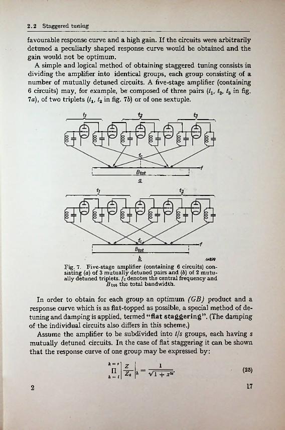
A simple and logical method of obtaining staggered tuning consists in dividing the amplifier into identical groups, each group consisting of a number of mutually detuned circuits. A five-stage amplifier (containing6 circuits) may, for example, be composed of three pairs [tv t2, tz in fig.7 a), of two triplets (tlf t2 in fig. 7b) or of one sextuple.
*2 *3
A 64flW
Fig. 7. Five-stage amplifier (containing 6 circuits) consisting (a) of 3 mutually detuned pairs and (6) of 2 mutually detuned triplets. /c denotes the central frequency and
B tot the total bandwidth.
In order to obtain for each group an optimum (GB) product and a response curve which is as flat-topped as possible, a special method of detuning and damping is applied, termed “flat staggering”. (The damping of the individual circuits also differs in this scheme.)
Assume the amplifier to be subdivided into l/s groups, each having s mutually detuned circuits. In the case of flat staggering it can be shown that the response curve of one group may be expressed by:
Z t _________n Zo VIT^’
l (25)h = l
172
Response curve of the complete amplifier 2
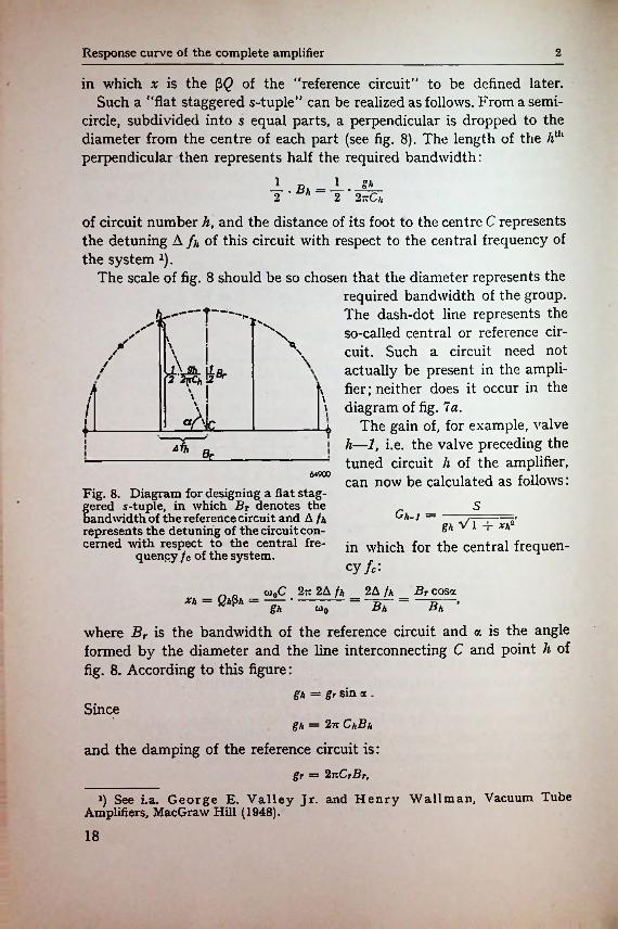
in which x is the of the ‘"reference circuit" to be defined later.Such a "flat staggered s-tuple" can be realized as follows. From a semi
circle, subdivided into s equal parts, a perpendicular is dropped to the diameter from the centre of each part (see fig. 8). The length of the hth perpendicular then represents half the required bandwidth:
1 Bj - 1 - 2 ' 2 2-0,
of circuit number h, and the distance of its foot to the centre C represents the detuning A /;, of this circuit with respect to the central frequency of the system *).
The scale of fig. 8 should be so chosen that the diameter represents therequired bandwidth of the group. The dash-dot line represents the so-called central or reference circuit. Such a circuit need not actually be present in the amplifier; neither does it occur in the diagram of fig. la.
The gain of, for example, valve h—1, i.e. the valve preceding the tuned circuit h of the amplifier, can now be calculated as follows:
—T—^AN
\s \
\V/\ \/
2Br// \V/ \/ o/'JcI
»Br
I
64900
Fig. 8. Diagram for designing a flat staggered 5-tuple, in which Br denotes the bandwidth of the reference circuit and A fh represents the detuning of the circuit concerned with respect to the central fre
quency /c of the system.
SGh-i —
gh V1 + Xli“‘
in which for the central frequency/*:
XJ _ QhQf — <»*C . 2~ fh _ 2A fh _ Br cosa
where Br is the bandwidth of the reference circuit and a is the angle formed by the diameter and the line interconnecting C and point h of fig. 8. According to this figure:
gh co„
gh = gr sin a .Since
gh = ChBh
and the damping of the reference circuit is:
gr = 2>TzCrBr,
q See i.a. George E. Valley Jr. and Henry Wallman, Vacuum Tube Amplifiers, MacGraw Hill (1948).
18
2.2 Staggered tuning
the value of x/t may be written:gr cos a _ cos a
gh ~ sin aassuming Cjt to be equal to Cr. Hence
= cot a,Xh =
GrGh-i = —:— ■■■-=
sin a V 1 -f cot2 aThe gain of each stage is therefore equal to that of a stage
in which the reference circuit is connected to the anode of the valve (at least as far as the central frequency is concerned). The total gain can thus again be calculated from the expression:
Gtofc = Gr11.
= Gr. (26)
At frequencies differing by A'/from the central frequency:
2(A/ + A7)Xh --- n ---
cos a + x sin a ’
where x = of the reference circuit. The response curve of circuit h is thus given by:
(27)Bh
lz sin a 1
Vsin2 a + cos2 a + x2 + 2x cos aZ, cos a + xh 1 + j sin a1 (28)
1 -j- x~ -j- 2iX cos a’
where Z0 — l/gr is the impedance of the reference circuit at zero detuning.If, for each of the circuits, the values of cos a are chosen according to the
construction in fig. 8, then 2):h = 8
n (1 + *2 + 2* COS oca) = 1 + tf23 • h -2
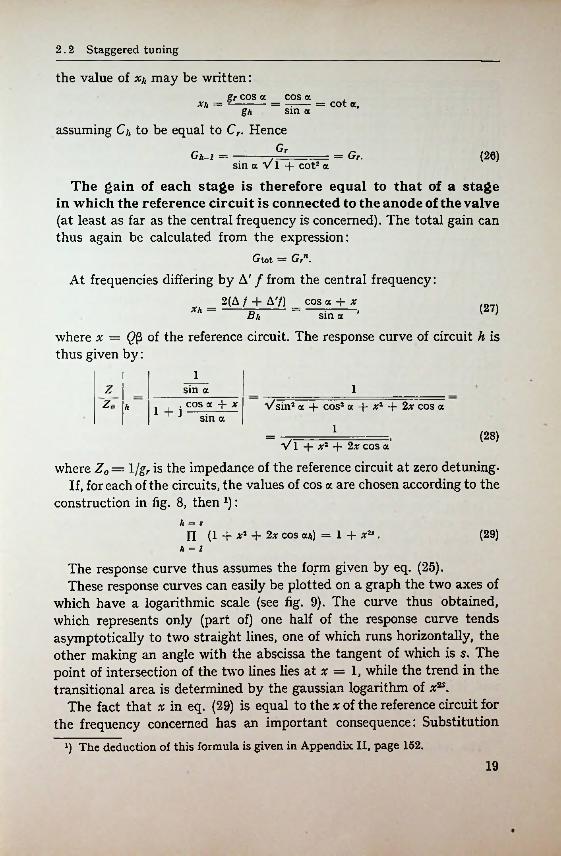
The response curve thus assumes the form given by eq. (25).These response curves can easily be plotted on a graph the two axes of
which have a logarithmic scale (see fig. 9). The curve thus obtained, which represents only (part of) one half of the response curve tends asymptotically to two straight lines, one of which runs horizontally, the other making an angle with the abscissa the tangent of which is s. The point of intersection of the two lines lies at x = 1, while the trend in the transitional area is determined by the gaussian logarithm of x2S.
The fact that x in eq. (29) is equal to the * of the reference circuit for the frequency concerned has an important consequence: Substitution
q The deduction of this formula is given in Appendix II, page 152.
(29)
19
Response curve of the complete amplifier 2
103 x = 1 in eqs (21) and (25) shows that the 3 db band- widths (Br of the reference circuit and the total band
it width Btot of the flat stag- 2 I gered s-tuple derived there
from) are identical. For a flat staggered group the bandwidth factor Fb is therefore equal to unity.
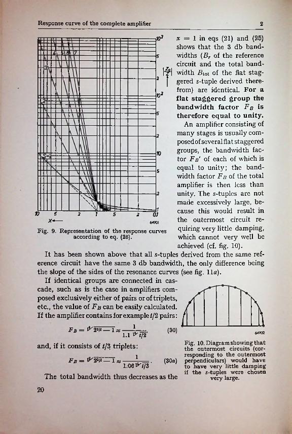
An amplifier consisting of many stages is usually composed of several flat staggered groups, the bandwidth factor Fb' of each of which is equal to unit}'; the bandwidth factor Fb of the total amplifier is then less than unity. The s-tuplcs are not made excessively large, because this would result in the outermost circuit requiring very little damping, which cannot very well be achieved (cf. fig. 10).
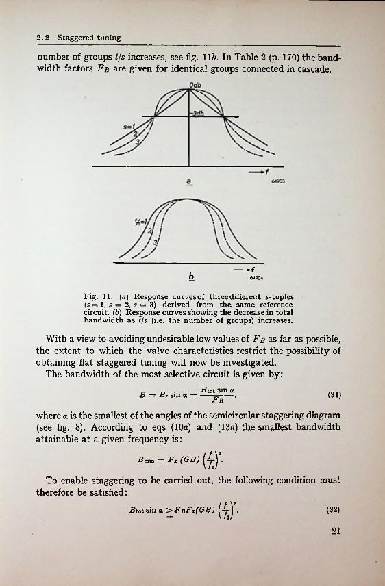
It has been shown above that all s-tuples derived from the same reference circuit have the same 3 db bandwidth, the only difference being the slope of the sides of the resonance curves (see fig. 11a).
If identical groups are connected in cascade, such as is the case in amplifiers composed exclusively either of pairs or of triplets, etc., the value of Fb can be easily calculated.If the amplifier contains for example 2/2 pairs:
Fb = r 2J/< — 1«
102
10
5
V 15 2 0764901
Fig. 9. Representation of the response curves according to eq. (25).
5X-----
K/
Hl (30) 64902
Fig. 10. Diagram showing that the outermost circuits (corresponding to the outermost
(30a) perpendiculars) would have to have very little damping if the 5-tuples were chosen
very large.
1.1 ^t/2
and, if it consists of tjZt triplets:1Fb = 23/< — l «
1.06l^//3‘The total bandwidth thus decreases as the
20
2.2 Staggered tuning
number of groups l/s increases, see fig. 116. In Table 2 (p. 170) the bandwidth factors Fb are given for identical groups connected in cascade.
b 64904
Fig. 11. (a) Response curves of three different s-tuples (s = 1, 5 = 2, s = 3) derived from the same reference circuit. (b) Response curves showing the decrease in total bandwidth as t/s (i.e. the number of groups) increases.
With a view to avoiding undesirable low values of Fb as far as possible, the extent to which the valve characteristics restrict the possibility of obtaining flat staggered tuning will now be investigated.
The bandwidth of the most selective circuit is given by:
Rtot sin aB = Br sin a = (31)Fb ’
where a is the smallest of the angles of the semicircular staggering diagram (see fig. 8). According to eqs (10a) and (13a) the smallest bandwidth attainable at a given frequency is:
•Smin — Fx (GB)
To enable staggering to be carried out, the following condition must therefore be satisfied:
Btot sin a >FbFx(GB) (32)
21
Response curve of the complete amplifier 2
ExampleFor a five-stage amplifier with six tuned circuits (GB) = 100, Fx = 0.8, fx =
300 Mc/s and / = 50 Mc/s.What is the maximum gain at 2?tot = 5 Mc/s if the selectivity of the circuits may
not be increased by adding extra capacitances?According to eq. (32) the following condition must be satisfied:
&■(GB_1.sin a > Fx.Fjj = B tottherefore:
sin a 100 / SO \*_>°.8 « 0.45.
In the case of one sextuple (see Table 3):sin a 0.261 = 0.26,Fs 1
which is insufficient. But in the case of two triplets:sin a _ 0.5 ~Fb ~ 0TS6 = 0.58,
which is sufficient, so that two triplets may be chosen, of which:5
F, Q-gg = 5.8 jVIc/s ,
while(GB) Fx 80G = G0 = 5J = 138’Br
whence follows from eq. (20):
Gtot = G5 = (13.S)5 = 450 000.
I
22
3 DISTORTION
3.1 DISTORTION IN DOUBLE SIDEBAND SYSTEMS
The method of flat staggering discussed in the previous section avoids decrease of the bandwidth as the number of circuits increases, as shown by fig. 11 b, and the response curve assumes a more rectangular form, as depicted in fig. 11a.
In one important respect this is an advantage, since not only does the amplitude characteristic of the frequency range passed become flatter, but the attenuation of undesired signals also increases. For this reason networks having a rectangular response curve are usually aimed at; but it should be recognized that such networks give rise to a fairly great distortion of certain signals.
This is not due to the amplitudes being incorrectly reproduced but to the phase being shifted. The response curve and phase characteristic of the customary networks are in fact so related that a rectangular form of the amplitude characteristic always gives rise to serious non-linearity of the phase characteristic x). If the phase characteristic of an H.F. or I.F. amplifier is linear (not necessarily constant) this merely results in the modulation being shifted over a constant time interval without the envelope of the modulated signal being distorted thereby, but if the phase characteristic is not linear the various modulation frequencies are mutually shifted in phase.
Therefore, although the distortion occurring in an amplifier is given in principle by its response curve, it is necessary in practice to know the phase characteristic in order to obtain a clear insight into the nature and seriousness of the phase distortion. The phase characteristic gives this information for sinusoidal signals of various frequencies in a form which does not show the distortion of non-harmonic waveforms and is therefore unsuitable for judging the quality of a video signal.
The common criteria for the reproduction of a video signal are adequate reproduction of the fine details present and the absence of false details. Since fine details are to be considered here as intensity variations of short duration, the reproduction of the high modulation frequencies is of particular importance.
For judging the fidelity with which high modulation frequencies are
x) Cf. Hendrik W. Bode, Network Analysis and Feedback Amplifier Design, Chapters XIV and XV, van Nostrand, New York.
23
Distortion 3
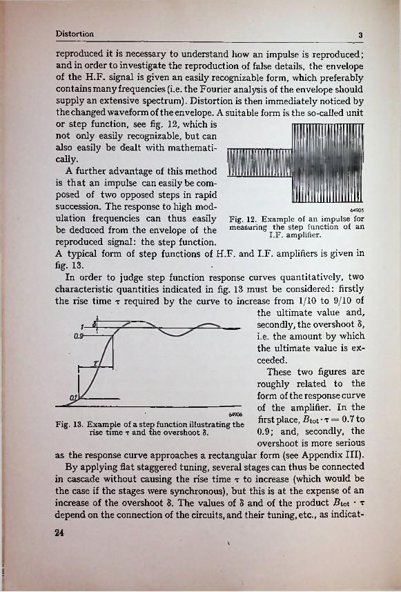
reproduced it is necessary to understand how an impulse is reproduced; and in order to investigate the reproduction of false details, the envelope of the H.F. signal is given an easily recognizable form, which preferably contains many frequencies (i.e. the Fourier analysis of the envelope should supply an extensive spectrum). Distortion is then immediately noticed by the changed waveform of the envelope. A suitable form is the so-called unit or step function, see fig. 12, which is not only easily recognizable, but can also easily be dealt with mathematically.
A further advantage of this method is that an impulse can easily be composed of two opposed steps in rapid succession. The response to high modulation frequencies can thus easily be deduced from the envelope of the reproduced signal: the step function.A typical form of step functions of H.F. and I.F. amplifiers is given in fig. 13.
In order to judge step function response curves quantitatively, two characteristic quantities indicated in fig. 13 must be considered: firstly the rise time t required by the curve to increase from 1/10 to 9/10 of
the ultimate value and, secondly, the overshoot 3, i.e. the amount by which the ultimate value is exceeded.
These two figures are roughly related to the form of the response curve of the amplifier. In the first place, Btot • t = 0.7 to 0.9; and, secondly, the overshoot is more serious
as the response curve approaches a rectangular form (see Appendix III).By applying flat staggered tuning, several stages can thus be connected
in cascade without causing the rise time t to increase (which would be the case if the stages were synchronous), but this is at the expense of an increase of the overshoot 3. The values of 3 and of the product Btot • t depend on the connection of the circuits, and their tuning, etc., as indicat-
64905Fig. 12. Example of an impulse for measuring the step function of an
I.F. amplifier.
64906
Fig. 13. Example of a step function illustrating the rise time t and the overshoot 8.
24
!
3.2 Distortion in vestigial sideband systems
ed in Table 3 (p. 172) where t, Btot ’t and Br • t are given for several identical groups of various composition connected in cascade.
It should be recognized, however, that the results quoted in this table apply only to double sideband systems; for single sideband reception the form of the step function response curve depends on other factors as well.
3.2 DISTORTION IN VESTIGIAL SIDEBAND SYSTEMSIn view of the considerable saving in bandwidth effected, the vestigial
sideband system (a form of single sideband transmission) is now commonly used, and it will be useful to investigate the changes to which the step function is subject if, throughout the transmitter and receiver, one sideband is suppressed.
This may be done by considering a carrier with a sinusoidally modulated envelope corresponding to the expression
sin a sin b = 1 cos (a—b) — -i cos (a + b),
where a represents the carrier frequency and b the modulation frequency. If throughout the whole system one sideband, e.g. the lower one, is suppressed, only the carrier plus the term — -J- cos (a + b) representing the upper sideband remains.
The same result would have been obtained by adding:— £ {£ cos (a — b) -f- £ cos (a + b)} (ml)
to the expression:£ {1 cos (a — b) — £ cos (a + 6)} , (m2)
giving again:— £ cos (a + b) .
As follows from the well-known trigonometrical equation, the added expression (ml) is equal to:
£ cos a cos b.
This manipulation clearly shows that the suppression of one sideband is equivalent to the addition of a fully modulated second carrier which is in quadrature with respect to the original carrier, its modulation also being in quadrature with respect to the original modulation. It is thus obvious that the original signal:
A0 sin 2k f0t- + Am sin 2w fmt • sin 2kf0t,
from which one sideband is suppressed, becomes:
A0 sin 2k/0/ -f £ A m sin 2nfmt • sin 2k/0< — £ A m cos 2nfmt • cos 2k/0/.25
Distortion 3
in which fm and f0 represent the frequency of the modulation and of the carrier, and Am and A0 represent the corresponding amplitudes.
The quadrature component (i.e. the cosine term) thus adds (in quadrature) to the original signal a modulation component which is out of phase and gives rise to distortion. It
-2 should further be noted that the modulation depth is approximate^ halved.
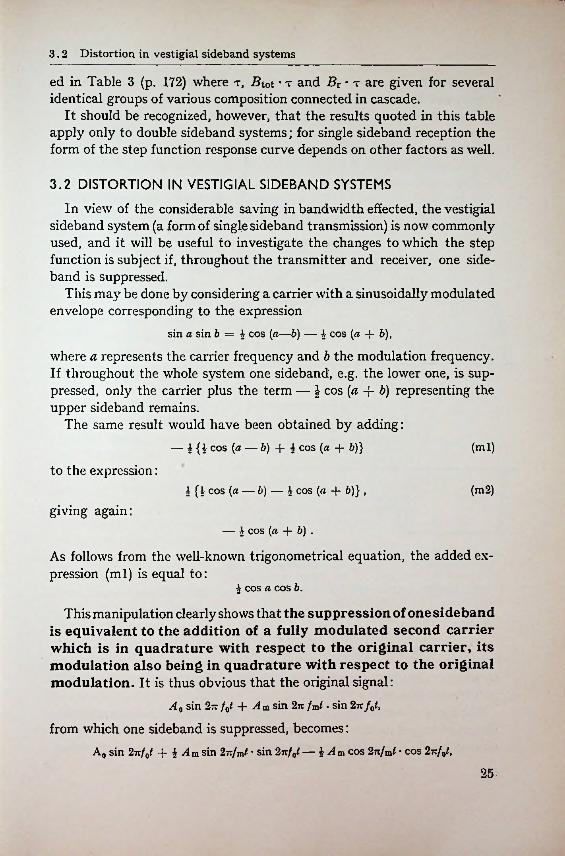
In practice the suppression of one sideband is achieved by means of a response curve of the form shown in fig. 14a, which
A can be considered equivalent to the sum of the curves represented in figs 146 and c. This corresponds to the mathematical analysis given above and, moreover, takes into ac-
- count the limited frequency range. It should be noted that the signal passed by the response curve of fig. 14c and that passed by the curve of fig. 146 are in quadrature.
The consequences of transmitting a modulated signal
A0 sin 2izf0t -f Am{ sin 2-xfmt • sin 2nf0t} == A0 sin 2tz/01 + IA m{ cos 2tz(/0 — fin)t — cos 2tz (/0 + /m)/ }
by a system having a response curve similar to fig. 14a will now be investigated more closely.
The image-symmetrical characteristic of fig. 146 gives rise to amplitude distortion onty of the sideband beyond the region from/4 to/3. The frequencies within this range correspond to modulation frequencies smaller than
i
j
i
fi fo 12 fti
Iii
f1 f0 *2i i
iii
i IIi
i'ii
iii*a fti
i
64907
Fig. 14. a Asymmetrical characteristic of a vestigial sideband system which may be considered as being composed of the sum of an image-symmetrical characteristic (6) and a radial-symmetrical charac
teristic (c).
26
3.2 Distortion in vestigial sideband systems
/3—f0 as shown by the above expression. The image-symmetrical response curve thus suppresses only modulation components with frequencies exceeding /3—/0. This is the normal phenomenon which also occurs in double sideband systems.
For all modulation components which are passed by the image-symmetrical response curve in the manner described above, the radial-symmetrical characteristic of fig. 14c adds a modulated H.F. signal to the carrier. This H.F. signal has the same frequency as the carrier, but, since it is in quadrature, the square of this signal must be added to the square of the
74Uk T -0.5/1.75
= -0.7/4.55 ; =1/1.25—2x4..5 Me 1^
/100 1.25/1.0 ^unit step— // ///f 2x2.625Mc/s60 i % /i // /4 0 1 /
120
*/o-20\__ _______________________________________L_-0.2 -0.1 0 0.1 0.2 0.3 0.4 0.5
69241
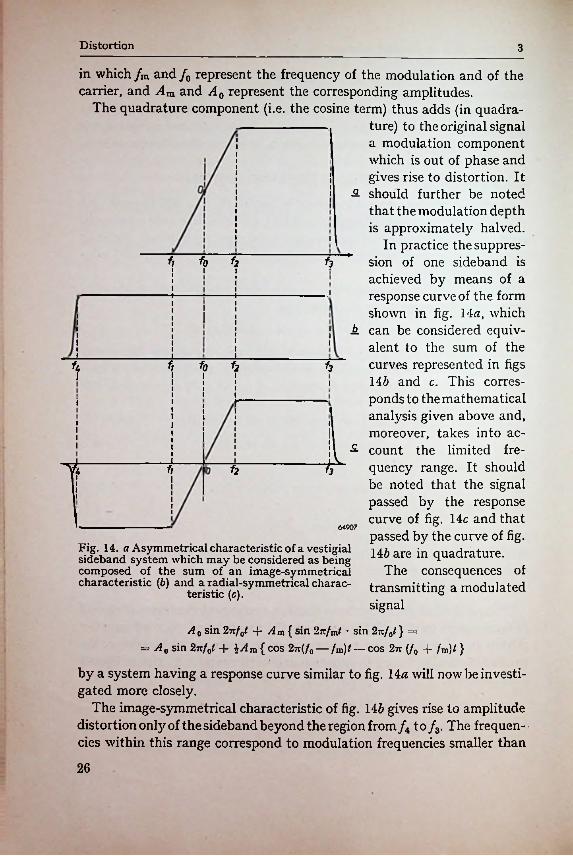
Fig. 15. Step functions of a single sideband system (full lines) with a modulation factor of 1 and an ideal filter. The total frequency band is 5.25 Mc/s. The broken lines
are valid for double sideband systems.
t(fjsec)
signal originating from the image-symmetricalc haracteristic represented in fig. 14b.
The above considerations apply without restriction to the modulation frequencies between f2—f0 and/3—f0, but from fig. 14c, demonstrating the identical attenuation of the two sideband components (of the quadrature component), it is clear that the quadrature component is smaller for frequencies below f2—f0 and tends to zero for modulation frequencies also tending to zero. This is emphasized here because the low frequencies form the most important contribution towards the video signal, and this effect renders it possible to reduce the distortion by the quadrature component for these frequencies.
It is clear that this favourable effect increases as the range from/^ to/227
Distortion 3
becomes greater, because the frequency range which takes advantage of the attenuation of the quadrature component then also increases. The response curve should therefore not be made too steep in the cut-off area on both sides of the carrier frequency.
The effect of the width of the cut-off area on the total bandwidth is illustrated by fig. 151), which shows the distortion of a voltage step (modulated on a carrier) whose components exceeding 4.25 Mc/s have been removed. The ratio (/0——fi) has been taken as parameter. The broken lines apply to double sideband systems.
The usual characteristics of the single sideband transmission are such that the range from f0 to fx can be given a maximum width of 1 Mc/s, the total bandwidth being approximately 5 Mc/s. The curve (/0 — /i)/ (/3 — /j) = 1/4.25 may thus be considered attainable in practice.
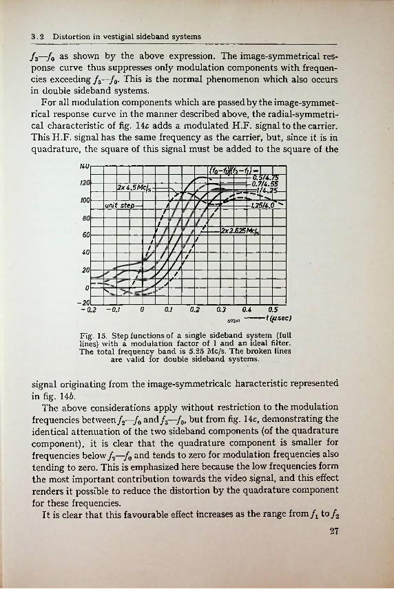
As a result of the square of the quadrature component having to be added to the square of the carrier, the importance of the quadrature component and therefore the distortion of the step function decreases with the modulation depth.
so
o
0.2 030 0.1-a;-02-03—(p sec)
64909
Fig. 16. Step function as shown in fig. 15 for (/0 — /i)/(/3 — /0) = 1/4.25, with the modulation factor m as parameter.
In fig. 162) the variation of one envelope of fig. 15 has been plotted for four different modulation depths m.
3.3 DISTORTION IN PRACTICAL AMPLIFIERS If the conditions imposed at the beginning of the above comments,
x) See Kell and’Fredendall, Selective Side Band Transmission in Television, R.C.A. Review, April 1940.28
3.3 Distortion in practical amplifiers
assuming the single sideband system to be ideal, are not satisfied, various consequences will result, as will become clear from Section 3.4.
As to the flatness of the response curve between /2 and /3 it can be stated that local deviations will result in incorrect reproduction of the corresponding modulation components. This will generally result in a transient with a frequency corresponding to the incorrectly reproduced modulation frequency, being added to the unit function response curve. Furthermore, the magnitude of the components in quadrature will change, so that too small a response of certain frequencies may be expected to give rise to relatively less distortion than too great a response.
The condition that the response curve of fig. 14a should be radial-symmetrical between fx and /2 with respect to point 0 may be expressed in another way, as follows:(1) the amplitude response at the frequency /0 should be half the value
obtained at frequencies between /2 and /3;(2) the sum of the responses of two frequencies between and /2 differing
from f0 by an equal amount should be twice the response at /0.If condition (1) is not satisfied this will give rise to an incorrect
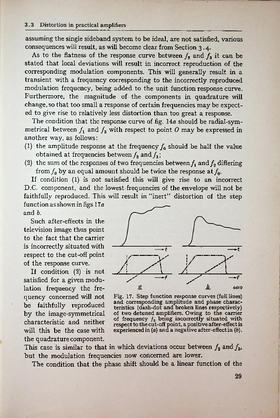
D.C. component, and the lowest frequencies of the envelope will not be faithfully reproduced. This will result in “inert” distortion of the step function as shown in figs 17a and b.
Such after-effects in the television image thus point to the fact that the carrier is incorrectly situated with respect to the cut-off point of the response curve.
If condition (2) is not satisfied for a given modulation frequency the frequency concerned will not Fig. 17. Step function response curves (full lines)
and corresponding amplitude and phase characteristics (dash-dot and broken lines respectively) of two detuned amplifiers. Owing to the carrier of frequency /0 being incorrectly situated with respect to the cut-off point, a positive after-effect is
will this be the case with experienced in [a) and a negative after-effect in [b).the quadrature component.This case is similar to that in which deviations occur between /2 and/3, but the modulation frequencies now concerned are lower.
The condition that the phase shift should be a linear function of the
I
!-----f
yA v' \ AA! V i—-f—-f
Aa 64910
be faithfully reproduced by the image-symmetrical characteristic and neither
.
:29
Distortion 3
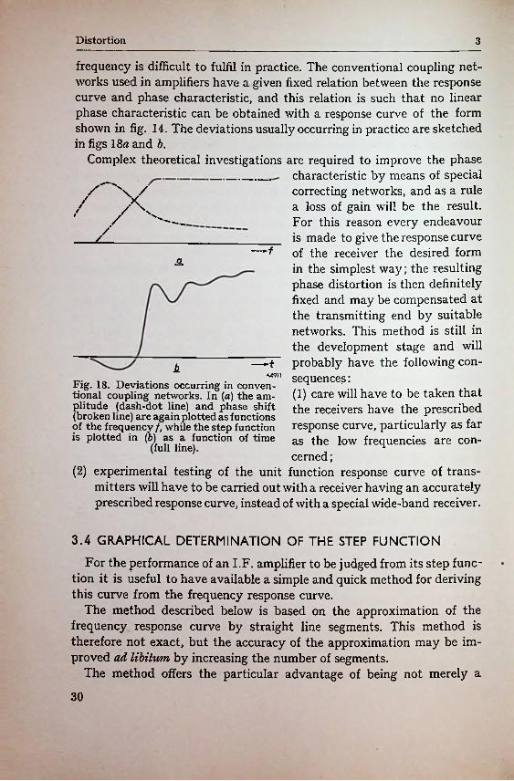
frequency is difficult to fulfil in practice. The conventional coupling networks used in amplifiers have a given fixed relation between the response curve and phase characteristic, and this relation is such that no linear phase characteristic can be obtained with a response curve of the form shown in fig. 14. The deviations usually occurring in practice are sketched in figs 18a and b.
Complex theoretical investigations are required to improve the phasecharacteristic by means of special correcting networks, and as a rule a loss of gain will be the result. For this reason every endeavour is made to give the response curve of the receiver the desired form in the simplest way; the resulting phase distortion is then definitely fixed and may be compensated at the transmitting end by suitable networks. This method is still in the development stage and will probably have the following consequences :(1) care will have to be taken that the receivers have the prescribed response curve, particularly as far as the low frequencies are concerned ;
(2) experimental testing of the unit function response curve of transmitters will have to be carried out with a receiver having an accurately prescribed response curve, instead of with a special wide-band receiver.
xy//9
/—- i
a.
—tKLQ \\
Fig. 18. Deviations occurring in conventional coupling networks. In (a) the amplitude (dash-dot line) and phase shift (broken line) are again plotted as functions of the frequency /, while the step function is plotted in (6) as a function of time
(full line).
b
3.4 GRAPHICAL DETERMINATION OF THE STEP FUNCTIONFor the performance of an I.F. amplifier to be judged from its step func
tion it is useful to have available a simple and quick method for deriving this curve from the frequency response curve.
The method described below is based on the approximation of the frequency response curve by straight line segments. This method is therefore not exact, but the accuracy of the approximation may be improved ad libitum by increasing the number of segments.
The method offers the particular advantage of being not merely a
30
3.4 Graphical determination of the step function
mathematical analysis but of giving also a clear insight into the relationship between the forms of the frequency response curve and the step function. From the graphical construction of the latter it can therefore be deduced how the frequency response curve should be changed to obtain a better step function. It is, for example, possible to investigate, by means of greatly simplified frequency response curves, how their various characteristic forms influence the step function 2).
In vestigial sideband systems the contribution of the quadrature components is determined separately, so that the influence of the modulation depth on the form of the step function can easily be investigated.
The effect of phase distortion is also determined separately, this being of importance for studying for example the value of phase correction in the transmitter. It is possible, therefore, to leave the phase distortion out of consideration for the time being, thus rendering the method more easily understood.
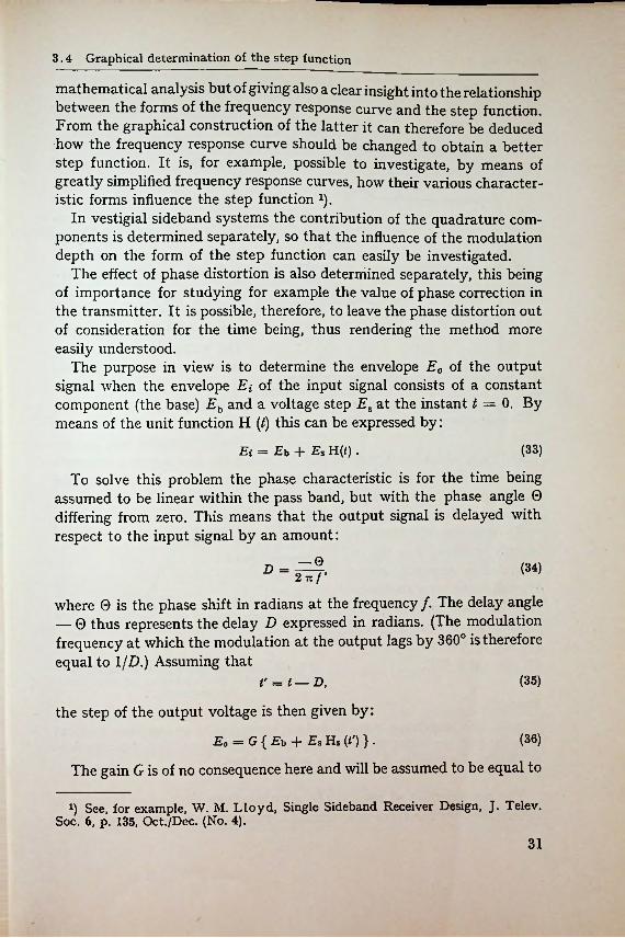
The purpose in view is to determine the envelope E0 of the output signal when the envelope E{ of the input signal consists of a constant component (the base) Eh and a voltage step Es at the instant t = 0. By means of the unit function H (t) this can be expressed by:
Ei = Eb + Es H(<).
To solve this problem the phase characteristic is for the time being assumed to be linear within the pass band, but with the phase angle 0 differing from zero. This means that the output signal is delayed with respect to the input signal by an amount:
(33)
— 0 (34)D =2 7T / '
where 0 is the phase shift in radians at the frequency /. The delay angle — 0 thus represents the delay D expressed in radians. (The modulation frequency at which the modulation at the output lags by 360° is therefore equal to 1 /D.) Assuming that
(35)tf = t — D,
the step of the output voltage is then given by:
E0 = G{Et> + EsHs {I') } .
The gain G is of no consequence here and will be assumed to be equal to
(36)
i) See, for example, W. M. Lloyd, Single Sideband Receiver Design, J. Telev. Soc. 6, p. 135, Oct./Dec. (No. 4).
31
Distortion 3
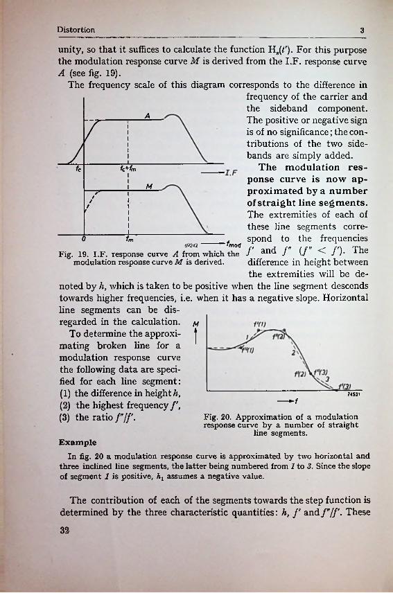
unit}', so that it suffices to calculate the function Ha(/'). For this purpose the modulation response curve M is derived from the I.F. response curve A (see fig. 19).
The frequency scale of this diagram corresponds to the difference infrequency of the carrier and the sideband component. The positive or negative sign is of no significance; the contributions of the two sidebands are simply added.
The modulation response curve is now approximated by a number of straight line segments. The extremities of each of these line segments corre-
. spond to the frequencies mod /' and /" (/" < /'). The
difference in height between the extremities will be de-
A
7Z
fc fc+fm
M*//
*m069242
Fig. 19. I.F. response curve A from which the modulation response curve M is derived.
noted by h, which is taken to be positive when the line segment descends towards higher frequencies, i.e. when it has a negative slope. Horizontal line segments can be disregarded in the calculation. M
To determine the approxi- | mating broken fine for a modulation response curve the following data are specified for each line segment:(1) the difference in height A,(2) the highest frequency(3) the ratio /"//'.
74531
Fig. 20. Approximation of a modulation response curve by a number of straight
line segments.Example
In fig. 20 a modulation response curve is approximated by two horizontal and three inclined line segments, the latter being numbered from 1 to 3. Since the slope of segment 1 is positive, assumes a negative value.
The contribution of each of the segments towards the step function is determined by the three characteristic quantities: h, /' and/"//'. These
32
3.4 Graphical determination of the step function
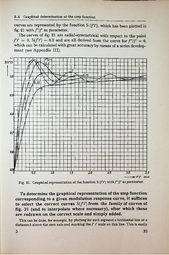
curves are represented by the function S (/'/'), which has been plotted in fig. 21 with f/f' as parameter.
The curves of fig. 21 are radial-symmetrical with respect to the point ft' = 0, S(ft') = 0.5 and are all derived from the curve for f/f = 0, which can be calculated with great accuracy by means of a series development (see Appendix III).
S(f't')
1.0
0.9
I0.8
0.7
0.6
0.50 1.5 2.0 2.5 3.0 3.50.5 1.0
-----------► f'f' 092-J4
Fig. 21. Graphical representation of the function S (/'/') with /"//' as parameter.
To determine the graphical representation of the step function corresponding to a given modulation response curve, it suffices to select the correct curves S (ft') from the family of curves of fig. 21 (and to interpolate where necessary), after which these are redrawn on the correct scale and simply added.
This can be done, for example, by plotting for each segment a horizontal line at a distance h above the zero axis and marking the f' t' scale on this line. This is easily
333
Distortion 3
done, since the time V — 1//' corresponds to the point /' V = 1 of fig. 21. At/' = 0 the curve passes through the point 0.5 h, with respect to which it is radial- symmetrical. For negative values of /' the zero axis may therefore be imagined to correspond with the line S (/'/') = 1 of fig. 21, etc. The graphical construction becomes clearer when instead of the zero axis the line S (/'/') = 0.5 is taken as basis. See, by way of example, fig. 33.
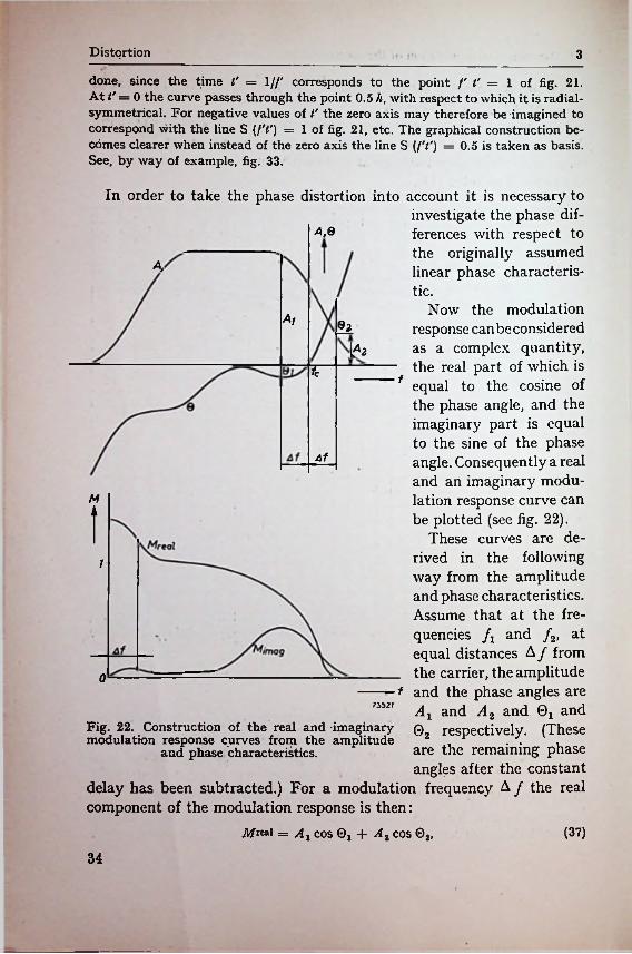
In order to take the phase distortion into account it is necessary toinvestigate the phase differences with respect to the originally assumed linear phase characteris-
A,Q
A
tic.Now the modulation
response can be considered as a complex quantity, the real part of which is
f equal to the cosine of the phase angle, and the imaginary part is equal to the sine of the phase angle. Consequently a real and an imaginary modulation response curve can be plotted (see fig. 22).
These curves are derived in the following way from the amplitude and phase characteristics. Assume that at the fre-
A, ®2
1*2fc
Af
M
i7
quencies and /2, at equal distances A f from the carrier, the amplitude0
f and the phase angles areAx and A2 and and
Fig. 22. Construction of the real and imaginary @ respectively. (These modulation response curves from the amplitude 2 1
and phase characteristics.
7352?
are the remaining phase angles after the constant
delay has been subtracted.) For a modulation frequency A / the real component of the modulation response is then:
(37)Mreal = Ax COS 0X - A% COS 02,
34
3.4 Graphical determination of the step function
and the imaginary component is:
Mining = — Ax sin + A2 sin 02.
(The lower sideband should be taken for A1 and the higher sideband for A 2, the sign of the phase distortion being thereby given.)
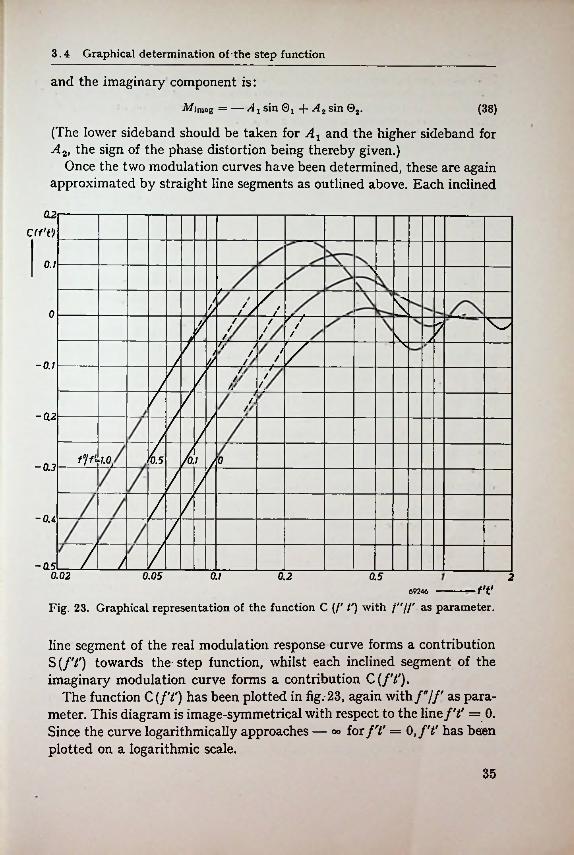
Once the two modulation curves have been determined, these are again approximated by straight line segments as outlined above. Each inclined
(38)
02C(f't')
0.1
//\// /£0 T-t/ /7 / 7/ / /L / \/ /7. V \/ /V / /A /-0.1 -/■/
/ //,/ /
/ /z/-0.2 /
/t /0.1f'If'=1.0, /°--0.3/ /
7 7-O.A /
7 /-0.50.02 0.05 0.1 0.2 0.5 2
ft169246
Fig. 23. Graphical representation of the function C (/' t') with /"//' as parameter.
line segment of the real modulation response curve forms a contribution S (/'/') towards the- step function, whilst each inclined segment of the imaginary modulation curve forms a contribution C(f't').
The function C (ft') has been plotted in fig. 23, again with /7/' as parameter. This diagram is image-symmetrical with respect to the line ft’ = 0. Since the curve logarithmically approaches — «> forf't' = 0, f't' has been plotted on a logarithmic scale.
35
Distortion 3
When no great accuracy is required, the C(f't') diagram can be approximated by a broken line, the descending part of which has a slope of 0.72 per decade. The transitional point is situated between 0.09 and 0.25, depending on the ratio /'//'. This procedure is followed in example 2 on p. 47.
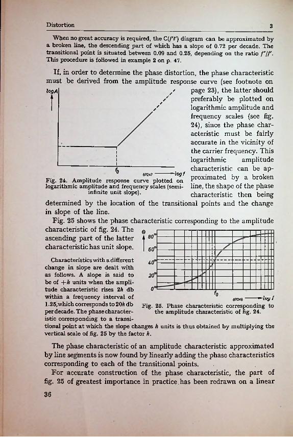
If, in order to determine the phase distortion, the phase characteristic must be derived from the amplitude response curve (see footnote on
page 23), the latter should preferably be plotted on logarithmic amplitude and frequency scales (see fig. 24), since the phase characteristic must be fairly accurate in the vicinity of the carrier frequency. This logarithmiccharacteristic can be approximated by a broken line, the shape of the phase characteristic then being
determined by the location of the transitional points and the change in slope of the line.
Fig. 25 shows the phase characteristic corresponding to the amplitude characteristic of fig. 24. The ascending part of the latter characteristic has unit slope.
Characteristics with a different change in slope are dealt with as follows. A slope is said to be of +k units when the amplitude characteristic rises 2k db within a frequency interval of 1.25, which corresponds to 20k db per decade. The phase characteristic corresponding to a transitional point at which the slope changes k units is thus obtained by multiplying the vertical scale of fig. 25 by the factor k.
The phase characteristic of an amplitude characteristic approximated by line segments is now found by linearly adding the phase characteristics corresponding to each of the transitional points.
For accurate construction of the phase characteristic, the part of fig. 25 of greatest importance in practice , has been redrawn on a linear
logA\
amplitude
4 logfFig. 24. Amplitude response curve plotted on logarithmic amplitude and frequency scales (semi
infinite unit slope).
69247
69248 •
Fig. 25. Phase characteristic corresponding to the amplitude characteristic of fig. 24.
36
3.4 Graphical determination of the step function
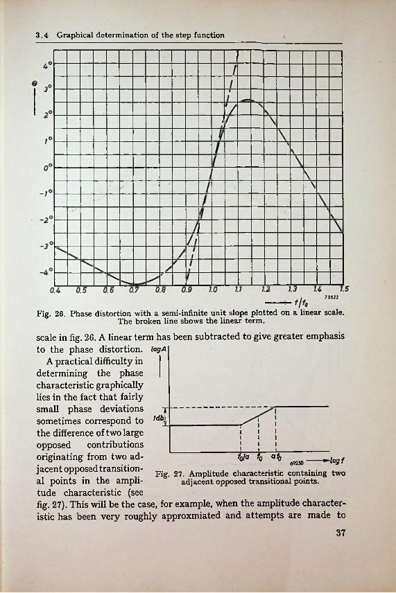
Fig. 26. Phase distortion with a semi-infinite unit slope plotted on a linear scale. The broken line shows the linear term.
scale in fig. 26. A linear term has been subtracted to give greater emphasis to the phase distortion. logA
A practical difficulty in determining the phase characteristic graphically lies in the fact that fairly small phase deviations sometimes correspond to the difference of two large
contributions
Jdbi
opposedoriginating from two adjacent opposed transitional points in the amplitude characteristic (see fig. 27). This will be the case, for example, when the amplitude characteristic has been very roughly approxmiated and attempts are made to
fo/a fo ah logfFig. 27. Amplitude characteristic containing two
adjacent opposed transitional points.
O9250
37
3Distortion
the accuracy of the construction by rounding off the curve. ^Forsuch purposes it will be advantageous to use the phase diagram of
Fig. 28. Phase diagram corresponding to the amplitude characteristic depicted in fig. 27. The parameter is the term a in fig. 27.
fig. 28, corresponding to the two opposed transitional points of the amplitude characteristic of fig. 27.
ExampleWhat will be the shape of the phase characteristic of a single resonant circuit
according to the above method? For large values of x:logA
d log A= 1.i \
/ l d log x/ \ in which\/ \/
\w0 W/\/ \/ \/ \ {See Appendix I)/ \/ \ Hence:/. \
d log A _ d log w Aw’
In the case of a very large detuning :
w0
0►logf Aw69252 >± 1._a C00
Fig. 29a. Rough approximation of the response whence curve of a single tuned circuit (fully drawn line). The actual response curve is indicated
by the dotted line.d log A >± 1.d log w
38
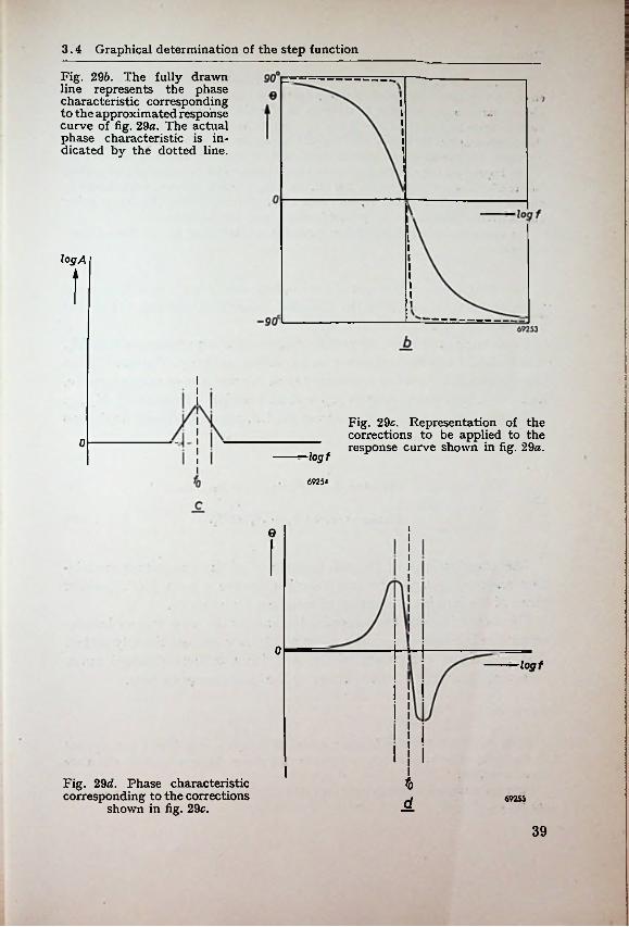
3.4 Graphical determination of the step function
Fig. 296. The fully drawn line represents the phase characteristic corresponding to the approximated response curve of fig. 29a. The actual phase characteristic is indicated by the dotted line.
logA
f
Fig. 29c. Representation of the corrections to be applied to the response curve shown in fig. 29a.0
logf
69254
0
0logf
IfoFig. 29d. Phase characteristic
corresponding to the corrections shown in fig. 29c.
69255£39
Distortion 3
When, as a first approximation, the response curve of the circuit is now represented by two straight lines, with slopes +1 and —1 (fully drawn lines, fig. 29a), the phase characteristic appears to conform to the diagram of fig. 25, provided its vertical scale is multiplied bij —2 (see fig. 296). In the case of very large detuning, this diagram agrees fairly well with the well-known arc tan function (see Appendix I) by which the actual phase characteristic (dotted line, fig. 296) is given.
The approximation of the amplitude characteristic can be improved by adding two corrections indicated in fig. 29c (cf. fig. 27). A phase correction as shown in fig. 29d must then be added to the phase characteristic, so that the actual phase characteristic (broken line in fig. 296) is very nearly approached.
The approximation can be further improved by increasing the number of these corrections.
Now that the contributions of the in-phase components have been dealt with, the determination of the so-called quadrature components of the step function will be investigated.
These components are derived from a modulation response curve Mq, which should also be considered as a complex quantity. The quadrature components can therefore be deduced from this modulation response curve, and are a real component Mqreal and an imaginary component Mq imag.
The derivation of these curves from the I.F. response curve is analogous to that of fig. 22, but now:
(39)•MqreaI = Ax COS 0X — Az COS 02,and
(40)Mqimag = Ax sin 0j + A 2 sin 02.
The contributions of the real component of the quadrature modulation response towards the step function assume a form jC(/T), whilst those of the imaginary component assume a form jS(/Y).
These contributions are determined in exactly the same way as described for the in-phase component, after which they are also linearly added. The quadrature component of the step function thus obtained must, however, be added in quadrature to the in-phase component.
Example 1
What shape does the step function assume at a voltage step from 1 to 2, applied to the input of an amplifier the amplitude and phase characteristics of which are given in fig. 30?
First the modulation response curves are determined for the in-phase component, see fig. 31.
40
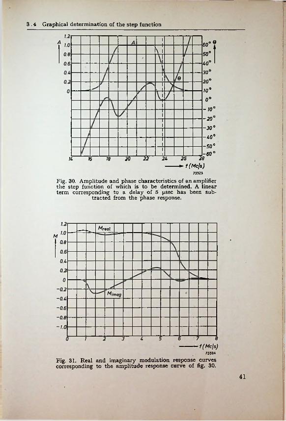
3.4 Graphical determination of the step function
o 06050°4 0°30°20°10°0°
-10° -20° -30° -4 0° -500 -60°
74 16 18 20 22 24 25 28------- ► f(Mcls)
73523
Fig. 30. Amplitude and phase characteristics of an amplifier the step function of which is to be determined. A linear term corresponding to a delay of 5 psec has been sub
tracted from the phase response.
!
i
73524
Fig. 31. Real and imaginary modulation response curves corresponding to the amplitude response curve of fig. 30.
41
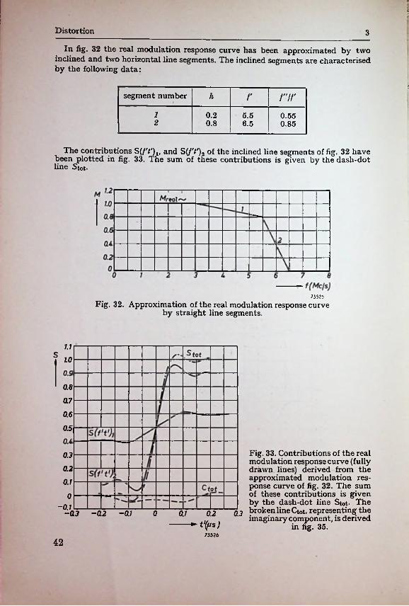
1
.
Distortion 3
In fig. 32 the real modulation response curve has been approximated by two inclined and two horizontal line segments. The inclined segments are characterised by the following data:
i
segment number h /' nri 0.2 5.5 0.552 0.8 6.5 0.85
The contributions S (/'/') x, and S(/'/')2 of the inclined line segments of fig. 32 have been plotted in fig. 33. The sum of these contributions is given by the dash-dot line 5tot-
^3525Fig. 32. Approximation of the real modulation response curve
by straight line segments.
7.7
10
0.8070.6
0.5
Fig. 33. Contributions of the real modulation response curve (fully drawn, lines) derived from the approximated modulation response curve of fig. 32. The sum of these contributions is given by the dash-dot line Stot- The
g j broken line Ctot. representing the imaginary component, is derived
in fig. 35.
0.3
0.20.1
0-o.l
-0.3 -02 -0.1 0 0.1 0.2 ----ttys)
7352642
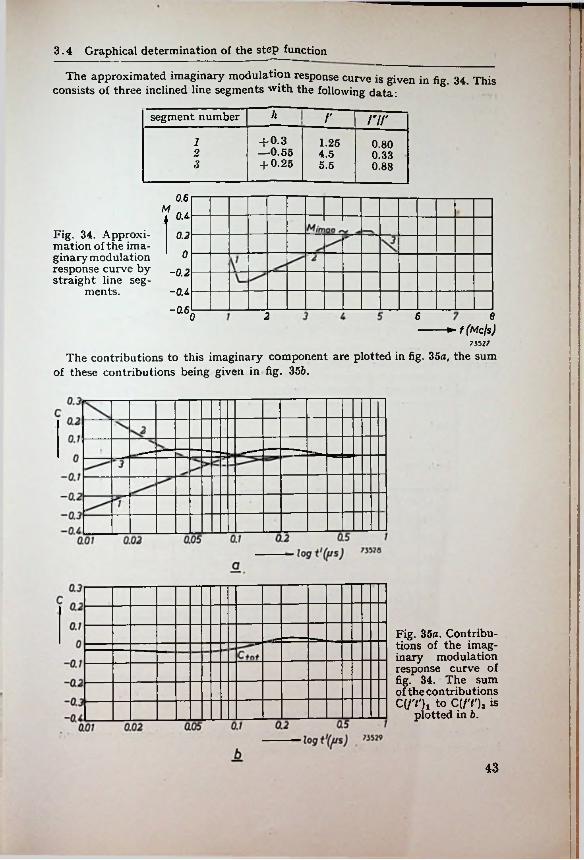
3.4 Graphical determination of the step function
The approximated imaginary modulation response curve is given in fig. 34. This consists of three inclined line segments with the following data:
hsegment number /' nr+ 0.3 —0.55 + 0.25
1 1.25 0.802 4.5 0.33 I3 5.5 0.88
0.6M „ . 0.4
Fig. 34. Approximation of the imaginary modulation response curve by straight line seg
ments.
0.2
0
-0.2-0.4
-0.6 2 6 a0--------► f(Mcjs)
75527
The contributions to this imaginary component are plotted in fig. 35a, the sum of these contributions being given in fig. 356.
Fig. 35a. Contributions of the imaginary modulation response curve of fig. 34. The sum of the contributions C(/T)i to C(/Y)s is
plotted in 6.
43
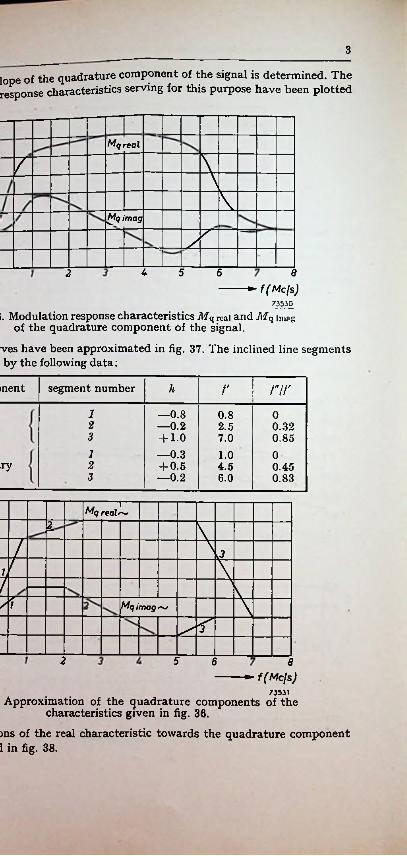
3
lope of the quadrature component of the signal is determined. The response characteristics serving for this purpose have been plotted
Mqreal
\7
Mq imag7s
4 5 6 82--------► f(Mc/s)
75530
i. Modulation response characteristics Mq real and Mq imog of the quadrature component of the signal.
ves have been approximated in fig. 37. The inclined line segments by the following data:
/' ! nrsegment number h>nent
1 —0.8 —0.2 + 1.0—0.3 + 0.5 —0.2
0.8 02 2.5 0.323 7.0 0.851 1.0 02 4.5 0.45■ry3 6.0 0.83
Mq real~2 \r %
iA Mq imag ~
2 5 6 8-------- ► i(Mcls)
75531Approximation of the quadrature components of the
characteristics given in fig. 36.
)ns of the real characteristic towards the quadrature component 1 in fig. 38.
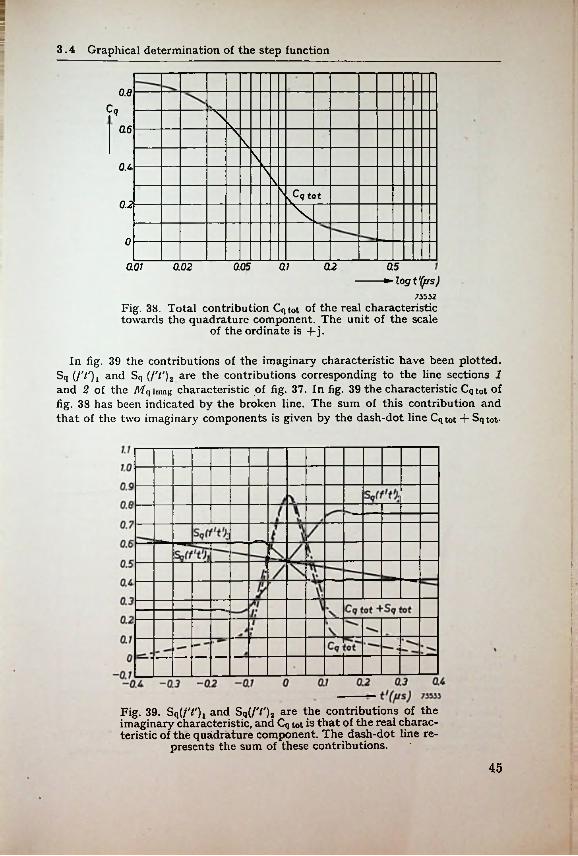
is 3.4 Graphical determination of the step function
0.8Cq \
0.6 \\\0.4 N \
\ .Cg tot0.2 V0
0.05 0.1 02 0.50.01 0.02-------^logt'(fis)
73552Fig. 38. Total contribution Cqtot of the real characteristic towards the quadrature component. The unit of the scale
of the ordinate is 4-j-
In fig. 39 the contributions of the imaginary characteristic have been plotted. Sq (/'/') x and Sq (f't')2 are the contributions corresponding to the line sections 1 and 2 of the Mqimng characteristic of fig. 37. In fig. 39 the characteristic Cqtot of fig. 38 has been indicated by the broken line. The sum of this contribution and that of the two imaginary components is given by the dash-dot line Cq tot + Sq tot-
!■
!!
i
Fig. 39. Sqf/T)! and Sq(/Y)2 are the contributions of the imaginary characteristic, and Cq tot is that of the real characteristic of the quadrature component. The dash-dot line re
presents the sum of these contributions.
45
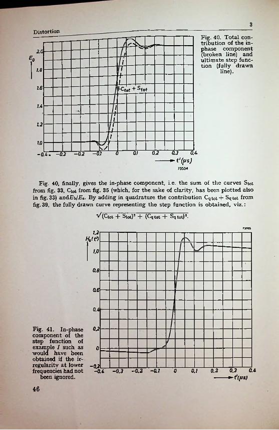
3Distortion
Fig. 40. Total contribution of the in- phase component (broken line) and ultimate step function (fully drawn
line).
fo I/ie\ +
L-Cfot * ^tot7.6
7.4tL7.2: T
4-
Ji7.0
0.2 0.3 0.4-------
73534
0.7-0.4. -0.2 -0.2 -0.7 0
Fig. 40, finally, gives the in-phase component, i.e. the sum of the curves Stot from fig. 33, Ctot from fig. 35 (which, for the sake of clarity, has been plotted also in fig. 33) andFb/Fs. By adding in quadrature the contribution Cqtot + Sqtot from fig. 39, the fully drawn curve representing the step function is obtained, viz.:
^ (Ctot + Stot)2 + (Cqtot + Sqtot)2-
73905
7.2,
7.0
0.0
0.6]
Fig. 41. In-phase 0.2 component of the step function of example 1 such as o would have been obtained if the irregularity at lower -qj_________________frequencies had not -0.4 -0.3 -0.2 -0.1
been ignored.0.7 0.2 0.3 0.4
------ —t'(ps)0
46
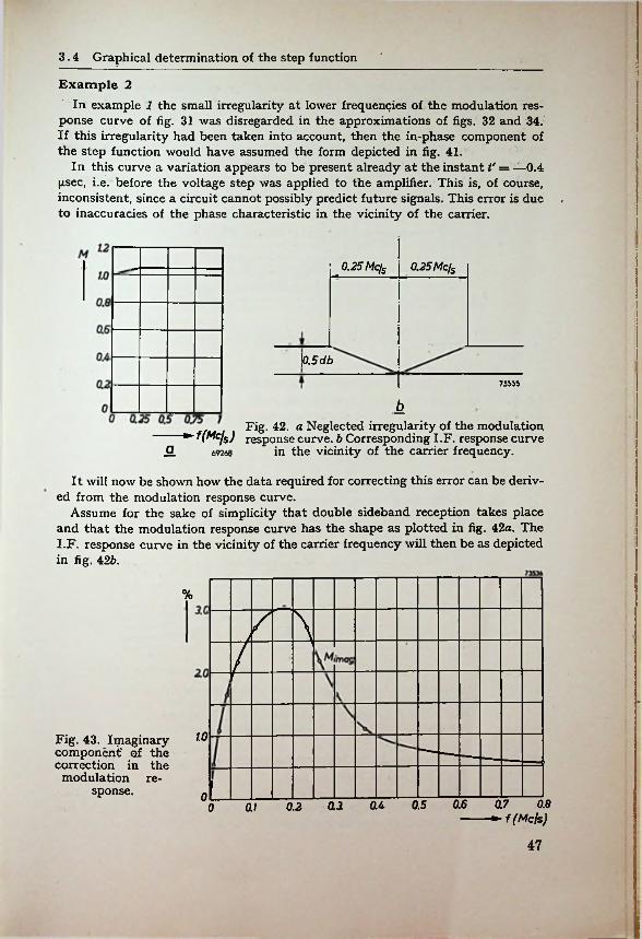
3.4 Graphical determination of the step function
Example 2In example 1 the small irregularity at lower frequencies of the modulation res
ponse curve of fig. 31 was disregarded in the approximations of figs. 32 and 34. If this irregularity had been taken into account, then the in-phase component of the step function would have assumed the form depicted in fig. 41.
In this curve a variation appears to be present already at the instant /' = —0.4 psec, i.e. before the voltage step was applied to the amplifier. This is, of course, inconsistent, since a circuit cannot possibly predict future signals. This error is due to inaccuracies of the phase characteristic in the vicinity of the carrier.
0.25 Mc/S 0.25Mc/s
■:
\0.5db
73535
b* Fig. 42. a Neglected irregularity of the modulation
► f(Mcfs) response curve, b Corresponding I.F. response curve Q. 69268 in the vicinity of the carrier frequency.
It will now be shown how the data required for correcting this error can be derived from the modulation response curve.
Assume for the sake of simplicity that double sideband reception takes place and that the modulation response curve has the shape as plotted in fig. 42a. The I.F. response curve in the vicinity of the carrier frequency will then be as depicted in fig. 42b.
%
5/
t10Fig. 43. Imaginary
component of the correction in the modulation re
sponse. 0q; 0.2 Q3 0.4 0.5 0.6 07 0.8
--------► f (Me Is)0
47
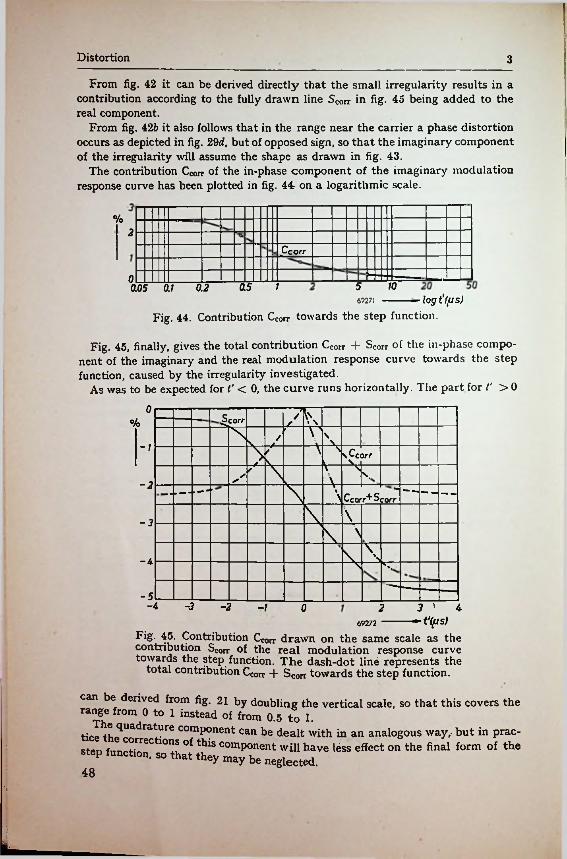
Distortion 3
From fig. 42 it can be derived directly that the small irregularity results in a contribution according to the fully drawn line SCOrr in fig. 45 being added to the real component.
From fig. 42b it also follows that in the range near the carrier a phase distortion occurs as depicted in fig. 29rf, but of opposed sign, so that the imaginary component of the irregularity will assume the shape as drawn in fig. 43.
The contribution Cc0rr of the in-phase component of the imaginary modulation response curve has been plotted in fig. 44 on a logarithmic scale.
%2
Ccorr
0 100.5 10.05 0.1 0.2logt'(fjs)69271
Fig. 44. Contribution Cc0rr towards the step function.
Fig. 45, finally, gives the total contribution CCOrr + SCOrr of the in-phase component of the imaginary and the real modulation response curve towards the step function, caused by the irregularity investigated.
As was to be expected for V < 0, the curve runs horizontally. The part for V > 00 / \NScorr% • \JL
\ In/ \v A-/ \X \ Ccorrk \\s✓ V%-2
\ Ccarr* Scorr\-3
\ \\\-4
-5-4 -3 —2 —/ 3 ' 4
► t'((JS)
Fig. 45. Contribution CCorr drawn on the same scale as the contribution SCorr of the real modulation response curve towards the step function. The dash-dot line represents the
total contribution CCOrr + SCOrr towards the step function.
0 269272
can be derived from fig. 21 by doubling the vertical scale, so that this covers the range from 0 to 1 instead of from 0.5 to 1.tice f"qUadra'ure comP°nent can be dealt with in an analogous way, but in prac-step functioT so that th^ C°mp°nent wiU have less effect on the final form of the:
48
i''
. -I
AGAIN, BANDWIDTH AND DISTORTION WITH FOUR-TERMINAL COUPLING NETWORKS
In the previous Sections the interstage couplings were assumed to consist of normal parallel tuned circuits, where necessary shunted by resistors, and the assumption was always made that for two successive stages the output voltage of the first stage is equal to the input voltage of the following stage. This will as a rule no longer be the case, however, if the coupling between the stages consists of more complex four-terminal networks.
The previous comments can, however, be extended to such networks by introducing the concept of transfer admittance. Whereas the admittance of a two-terminal network is understood to be the current divided by the voltage at the same pair of terminals, the no-load transfer admittance of a four-terminal network is here taken to be the current at the input terminals divided by the voltage at the unloaded output terminals. (The concept of transfer impedance can be defined in a similar way.)
Assuming again that the feedback in the valve is negligible and considering the input valve as a current source V{ • Sen, shunted by its internal resistance ra and its anode admittance g0 + jcoC0, then it is obvious that the gain of stage h can be written as:
. ' _ . _i_ =___(Vi)h Yh,h+1 (Vi)h Yh,h+1
•Soff(IT)a+2 (41)Gh =
where Y/„/,+i represents the transfer admittance Ii/V0 of the coupling network between the stages h and h + 1, including at the input side the admittance:
1
l— + go + j<oCp,Ya
and at the output side the admittance:gi + j <oC{.
For the interstage couplings now to be dealt with, it thus suffices to substitute Yhth+1 for Y. This having been done, the calculations can be worked out in an analogous way.
Two examples of a four-terminal coupling network, namely a so-called 'V* network and a double-tuned band-pass filter, are discussed below.
The ‘ V' network (fig. 46) is equivalent to a normal single-tuned circuit the input and output of which are ‘Tapped”, as a result of which the total circuit capacitance is reduced, since the capacitances C0 and C* longer in parallel as in a single-tuned circuit. For a given frequency the
;iii
■
■i
••
are no
494
;!
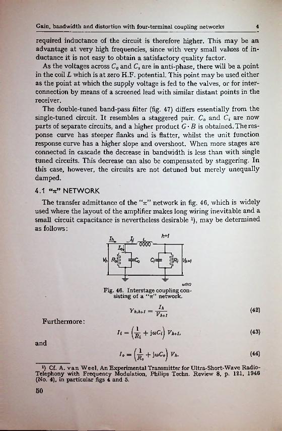
Gain, bandwidth and distortion with four-terminal coupling networks 4
required inductance of the circuit is therefore higher. This may be an advantage at very high frequencies, since with very small values of inductance it is not easy to obtain a satisfactory quality factor.
As the voltages across C0 and Ct are in anti-phase, there will be a point in the coil L which is at zero H.F. potential. This point may be used either as the point at which the supply voltage is fed to the valves, or for interconnection by means of a screened lead with similar distant points in the receiver.
The double-tuned band-pass filter (fig. 47) differs essentially from the single-tuned circuit. It resembles a staggered pair. C0 and C; are now parts of separate circuits, and a higher product G- B is obtained. The response curve has steeper flanks and is flatter, whilst the unit function response curve has a higher slope and overshoot. When more stages are connected in cascade the decrease in bandwidth is less than with single tuned circuits. This decrease can also be compensated by staggering. In this case, however, the circuits are not detuned but merely unequally damped.
4.1 “tc” NETWORKThe transfer admittance of the ‘ V’ network in fig. 46, which is widely
used where the layout of the amplifier makes long wiring inevitable and a small circuit capacitance is nevertheless desirable 1), may be determined as follows:
/)+/Il lIo\\
Vh R0\ 'Qj Cj Vh+1\Ri
04912Fig. 46. Interstage coupling con
sisting of a “tc” network.
= jL (42)
Furthermore:7i = (-l+jcoCi)
Io = (iT0 +j<oCo)
(43)VMand
(44)Vh.
*) Cf. A. van Weel, An Experimental Transmitter for Ultra-Short-Wave Radio- Telephony with Frequency Modulation, Philips Techn. Review 8, p. 121, 1946 (No. 4), in particular figs 4 and 5.
50
4.1 "7c” Network
Moreover: :.Vh= Vh+1 + IijuL. (45) .
From eqs (45) and (43):(±' + ]<*L,Vh = V,l+1 -f- (46)
(and from eqs (46) and (44):
= (i- + juC„)| (i. + jt0Ci) Vj,+i jwZ. |.I, V/,+1 + (47)
i CSince //* = I{ + I0> eq. (42) finally becomes:
VhM = Tow2L + w) + jo)Co + j<oCi + WRii i! fjco3LC0Ci. (48) '• ftAt resonance the imaginary part of eq. (48) is zero, which gives:
Co + Q + l^Ri
'■ :
!= co2LC0C|,
:1 ■ 'Iwhence:\= z(k + ii) 1 (49)co2 Co Ro Ci Ri
A simplification can be introduced b)' making the following approximation :
ti
= i(r0 + i)- (50)Wo2
At or near resonance the real part of Yh,h+i is therefore approximately: ..:(cr„+ zij (si + si) - _ (/§b + -mi}- (51)(y"'"+i)real ~ Tto + 1
Ri~
The negative sign, which is of no consequence here, will henceforth be omitted.
To determine the bandwidth the imaginary part at co ^ co0 must be calculated:
= to { (Ci + Co) + ^
or, if LjRiR0 is ignored and co(co + co0)/co02 is set equal to 2,
^(Ci + c.) {.^ Yh,h+1 jimaginary
^ Yh,li+1 j = 2 A co (Ci -p Co), (52)imaginary
provided Aw/co0 is small. (It should be noted that for very low frequencies the transfer admittance does not assume the very high value which might
i
i51
I;.i
Gain, bandwidth and distortion with four-terminal coupling networks 4
be expected from this approximated formula.) To determine the frequency at which the attenuation is 3db, the. imaginary part must be set equal to the real part, that is to say:
Co Ci (53)2Aw (C» -f Co) — + RoCo
This expression may be adapted to the previous comments by writing:l (54)Ri = gi + gci'
andl (55)JjT = So + gco,
where g0 -j- gco is assumed to include l/ra of the valve. Hence:
27~B(Ci + Co) = (gi + gci) • Q + (go + gco) •
This equation thus replaces eq. (6). The gain per stage now follows from:
G =
(56)
S 5 (57)Yh,h+1
(gi + gci) ' 7=r + (go + gco) *Ci
Combining eqs (57) and (56) again gives:S (8)(GB) =
27t (Ci -}- Co)
The further procedure is similar to that given in Sections 1 and 2, provided gi + g0 is replaced by:
CiCogi'cl + g"' C~„-
This means that /x and /0 must be replaced by:fi" = Y2/1* (58)
and(59)hu = Y2/0.
in which:I / gi Co ' go Ci -| / Co ,Y2 “ V gi + go Ci~^ gi + go Co~\ Ci~ (60)
since g{> g0.
In practice may be set equal to fv The quantities Fs, Fb and Fx remain unchanged, so that the theory of the previous sections also applies to amplifiers where the interstage coupling is formed by the ‘V’ network of fig. 46.
52
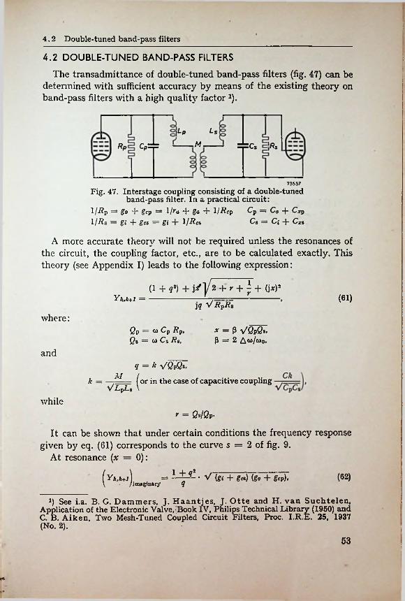
:4.2 Double-tuned band-pass filters
4.2 DOUBLE-TUNED BAND-PASS FILTERSThe transadmittance of double-tuned band-pass filters (fig. 47) can be
determined with sufficient accuracy by means of the existing theory on band-pass filters with a high quality factor *).
Ls\Lp
M | RsRp Q>=r
73537Fig. 47. Interstage coupling consisting of a double-tuned
band-pass filter. In a practical circuit:1/I?P = go + gcp = 1/^a + ga 4" l/i?cp Cp = Co -}- Crp l/Rs = gi + gcs = gi -p 1/Rcs Cs = Ci -f- Cxs
A more accurate theory will not be required unless the resonances of the circuit, the coupling factor, etc., are to be calculated exactly. This theory (see Appendix I) leads to the following expression:
(1 + q2) + j./]/2 + r+± + (j*r-(61)Yfi.h+1 =
jq V RpRswhere:
x = P VQpQ;P = 2 Aw/wo,
Qp — <o Cp Rp, Qs = w Cs Rs,
andq = k VQpQs.
M (k = (or *n case °* capacitive coupling
whiler — Qs/Qp-
It can be shown that under certain conditions the frequency response given by eq. (61) corresponds to the curve s = 2 of fig. 9.
At resonance (x = 0):
^FA,A+lj = 1 +-q~ * V (gi -+- gcs) {go + gcp), (62)qimaginary
q See i.a. B. G. Dammers, J. Haantjes, J. Otte and H. van Suchtelen, Application of the Electronic Valve, Book IV, Philips Technical Library (1950) and C. B. Aiken, Two Mesh-Tuned Coupled Circuit Filters, Proc. I.R.E. 25, 1937 (No. 2).
53
Gain, bandwidth and distortion with four-terminal coupling networks 4
from which, by means of eq. (41), the gain per stage is:
G =------------- 5 —------1__ .V (gi + gcs) (go + gcp) 1 + ?2' (63)
By setting:dZh,h+i _ d-Zh,h+i d*Zh,/,+i
= 0,dx dx~ dx3i
at x = 0, the value of q can be found at which the top of the response curve is flattest. It can be proved that at this condition (see Appendix I):
(64)<7
If this condition is satisfied, so-called transitional coupling is obtained. In that case the frequency response corresponds to that shown in fig. 9, s = 2, and:
±nBVCoCi = 2VT + q*V(gi + gcs) (g0 + acp).The maximum product of gain and bandwidth achievable by minimiz
ing the capacitances may now be expressed by:
(65)
5 2<7G • B = (66)4tc VC0Ci Vl + q2
This expression will be so interpreted that the first factor is considered as the (GB) product in the case where the coupling consists of a bandpass filter, and the second factor as the bandwidth factor in that case. This (GB) product is thus:
S(GB)0 =----t=.4tz V C0CJi
This (GB)" product is identical to that given in Section 1, provided Ci = C0. In practice these capacitances do not differ greatly, so that, in this case too, the theory of Section 1 remains valid to all intents and purposes. The stray capacitances can of course also be taken into account, giving:
(67)
SFx"(GB)" =4izV (Ci + Cas) (Co + Cap)
where C« = the stray capacitance across the secondary and Cox — the stray capacitance across the primary.
Hence:
*v=y Ci Co (68)Ci + Cars Co -J- Cxp
54
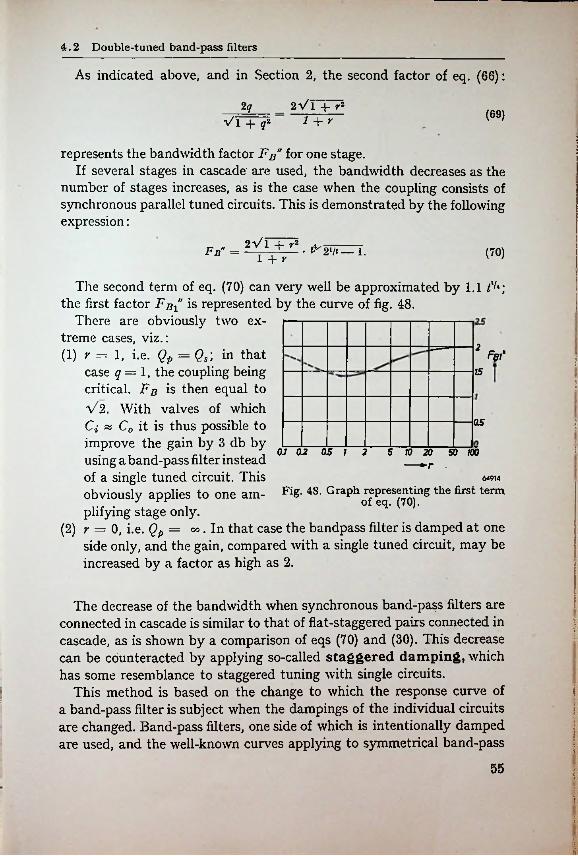
4.2 Double-tuned band-pass filters
As indicated above, and in Section 2, the second factor of eq. (66):
2VT + y- 1 + r
2 q (69)Vl +
represents the bandwidth factor Fb" for one stage.If several stages in cascade are used, the bandwidth decreases as the
number of stages increases, as is the case when the coupling consists of synchronous parallel tuned circuits. This is demonstrated by the following expression:
!
2vT + r2 • \y 2lli— 1.Fb" = (70)1 + v
The second term of eq. (70) can very well be approximated by 1.1 tl,i; the first factor Fb\ is represented by the curve of fig. 48.
There are obviously two extreme cases, viz.:(1) r = 1, i.e. Qp=Qs] in that
case q = 1, the coupling being critical. FB is then equal to V2. With valves of which Ci « C0 it is thus possible to improve the gain by 3 db by using a band-pass filter instead of a single tuned circuit. This obviously applies to one amplifying stage only.
(2) r = 0, i.e. Qp= «>. In that case the bandpass filter is damped at one side only, and the gain, compared with a single tuned circuit, may be increased by a factor as high as 2.
2 Fb,'15
05
0J 02 05 1 2 5 10 20 50 100
64914
Fig. 48. Graph representing the first term ofeq. (70).
The decrease of the bandwidth when synchronous band-pass filters are connected in cascade is similar to that of flat-staggered pairs connected in cascade, as is shown by a comparison of eqs (70) and (30). This decrease can be counteracted by applying so-called staggered damping, which has some resemblance to staggered tuning with single circuits.
This method is based on the change to which the response curve of a band-pass filter is subject when the dampings of the individual circuits are changed. Band-pass filters, one side of which is intentionally damped are used, and the well-known curves applying to symmetrical band-pass
; i:
55 i
•:
;
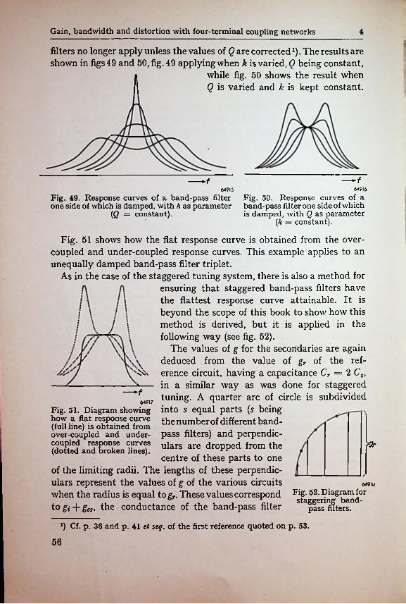
Gain, bandwidth and distortion with four-terminal coupling networks 4
filters no longer apply unless the values of Q are correctedx). The results are shown in figs 49 and 50, fig. 49 applying when k is varied, Q being constant,
|» while fig. 50 shows the result whenII Q is varied and k is kept constant.
—*f6491664915
Fig. 49. Response curves of a band-pass filter Fig. 50. Response curves of a one side of which is damped, with k as parameter band-pass filter one side of which
(Q = constant). is damped, with Q as parameter (k = constant).
Fig. 51 shows how the flat response curve is obtained from the overcoupled and under-coupled response curves. This example applies to an unequally damped band-pass filter triplet.
As in the case of the staggered tuning system, there is also a method for ensuring that staggered band-pass filters have the flattest response curve attainable. It is beyond the scope of this book to show how this method is derived, but it is applied in the following way (see fig. 52).
The values of g for the secondaries are again \ deduced from the value of gr of the ref-
erence circuit, having a capacitance Cr — 2 Cs, *— in a similar way as was done for staggered
*"Cj9i7 tuning- A quarter arc of circle is subdivided Fig. 51. Diagram showing into s equal parts (s being
a fla.t response curve ^he number of different band- (full line) is obtained fromover-coupled and under- pass filters) and perpendic-?°uPle,d r“Pon,f curves ula are dropped from the(dotted and broken lines).
centre of these parts to onep^-
of the limiting radii. The lengths of these perpendiculars represent the values of g of the various circuitswhen the radius is equal to gr. These values correspond FlS-52• Diagram for i i ° . , . . n., staggering band-to gi + gcs, the conductance of the band-pass niter paSs filters.
6491i)
J) Cf. p. 36 and p. 41 et seq. of the first reference quoted on p. 53.
56
; :
I4.2 Double tuned band-pass filters
!secondary being denoted by gC5 (the primary conductance g0 being assumed to be zero).
The resulting bandwidth is now equal to that of the reference circuit given by:
.
]r
2tt BrCr = gr,
provided the coupling of each of the band-pass filters is adjusted to the correct value. This will be the case when:
£ _ _L _ &Qr MoCr
Under these conditions the gain per stage follows from the value of | | at resonance, viz. (see Appendix 1^):
| Yh,h+i! = 2- fk VCsCP,
(71)
(72)
giving:
gr ' CpS
2nBrV CsCp
at A/ = 0, and since the bandwidth B is equal to Bx:5 (73)G- B = Fx"Fb"(GB)" =
2k"\/ CsCp
Substitution of (GB)" from eq. (67) now shows that for an amplifier with double tuned coupling circuits the secondaries of which are stagger- damped, Fb" is always equal to 2.
The response curve of a set of flat staggered band-pass filters can again be derived from fig. 9, where s is the total number of tuned circuits. Since each band-pass filter comprises two tuned circuits, s is in general an even number. It is, however, possible to make a combination of stagger- damped band-pass filters with one single “fill-up” circuit, which is tuned to the central frequency. In this way overall response curves can be obtained which correspond to the odd values of s in fig. 9.
As in the case where single circuits are used, the number of elements of the staggered group should not be made too large; as a rule groups consisting of pairs or triplets are used. If such groups are connected in cascade, the total bandwidth decreases only very slightly (see Table 4, p. 172). This is due to the response curves of staggered band-pass filter groups having very sharp corners. As may be expected, the overshoot percentage is quite considerable (see Table 3, p. 172).
The possibilities of staggering are restricted also in the case of band-pass filters, owing to the limit imposed on the most selective secondary circuit
;;
!\ ■
i
57.
bandwidth and distortion with four-terminal coupling networks 4Gain,
(only the secondaries of the band-pass filters are damped, Rt thus being much smaller than 2?p). The following condition must be satisfied:
Biot sin a 2> Fb’Fx'(GB)’ (jj ]/Co Cox Ci -f- Cix
(74)
With amplifiers having single tuned interstage circuits the quantity fx determined by the sum of gi -f go- When band-pass filters are used giwas
and go are separated by the band-pass filter, but since in practice gi is much larger than g0, so that gi + g0 is almost equal to gi, there is no need to introduce here a new quantity f{.
If a band-pass filter is used at the input of the amplifier the quality factors of the primary and secondary are made identical, which means that r — 1, so that this band-pass filter cannot very well be included in the staggering scheme. There are also other reasons for making the first band-pass filter less selective than the other circuits, especially in superheterodynes intended for reception of several channels. Moreover, by not including the input circuit in the staggering scheme, this circuit can be chosen to meet specific requirements. For example, the input circuit must also satisfy special conditions as to reflection-free termination of theaerial cable.
The selectivity of the input circuit is already reduced by the heavy damping caused by the valve and aerial. To ensure that the termination of the aerial cable is such that no reflections occur, the following condition must be satisfied:
ftant = = 2Zt', (75)where Zi is the input impedance of the band-pass filter (at the resonant frequency) with the aerial disconnected and Zi is the input impedance when the aerial is connected.
Now{
1 + q'2 ftp ftnnt’
where q'2 — k2QvQs in the case of a connected aerial.Hence, the condition to be satisfied becomes:
■ftp — ftnnt■ftp + ftant
In the important case in which Rp is very high, q' should be made approximately equal to unity.
By means'of the formulae for band-pass filters it can be calculated that (for Cx = 0) the product G • VB of the aerial circuit is then approximately 1.2 times that of a single-tuned aerial circuit.
A further advantage of this circuit compared to the single circuit is that less trouble is experienced from reflections at the sideband frequencies.
ftnntZi' =
<?'2 = (76)i
58
'n11
5 NOISE
5.1 DEFINITIONS
The signal-to-noise ratio at the output of a receiver is of considerable importance. This ratio is determined by the signal-to-noise ratio of the signal source and by the inherent noise of the amplifier. Different effects must therefore be combined for calculating the final signal-to-noise ratio. Noise voltages cannot, however, be simply added and it is the mean squares of the noise voltages or the noise powers in one and the same resistance which are additive. It is therefore useful to express signal-to-noise ratios not as ratios of signal and noise voltages but as ratios of powers, the more so as the essential problem in most amplifiers for metric waves is power gain.
Basing the considerations on these lines it is logical to introduce the concept of available power, i.e. the power obtainable from the source concerned at optimum matching. For a signal source with a no-load signal voltage Es and an internal resistance Rs this power is:
i
Erp* - ik.
Similarly, the available noise power of the signal source is:
p pn .n “ 4Rs’
the noise voltage En2 is defined with greater accuracy later. It is obvious that no purpose is served by considering noise outside the pass-band of the amplifier.
The signal-to-noise ratio at the input of an amplifier is now taken to be Psi/Pni, whether the amplifier is correctly matched to the signal source or not. This ratio obviously is a characteristic of the signal source.
The available powers of the signal and noise at the output of an amplifier are denoted by Pso and Pno respectively, and at a given matching between signal source and amplifier the signal-to-noise ratio is Pso/Puo. At this matching the noise factor N is by definition:
;;
I■
..I
,v - PsilPni- PSo/Pno
(77)
The noise factor N thus indicates to what extent the signal-to-noise ratio59
:
iNoise 5
deteriorates when the signal passes through the amplifier 1). N is not a characteristic of the amplifier considered but of the amplifier with the signal source to which it is to be connected. Eq. (77) gives a somewhat different impression if it is written:
P no PnoN = (77a)p P$p Pni * (Gp)iFn'"p7i
In eq. (77a) the numerator represents the total available output noise,1. e. the sum of the noises originating from the signal source and the amplifier under the given conditions. The denominator represents the available input noise Pni multiplied in the same ratio as the signal power Psi- In the third member of eq. (77a) this gain is denoted by (Gp)s, the “available power gain”. If no additional noise were introduced by the amplifier the denominator would obviously be identical to the available output noise. The noise factor N considered in this way thus represents the ratio, at the output, of the total noise from the signal source and amplifier to the noise originating from the signal source alone. This and the former definition are obviously concordant and each has its merit.
The last definition clearly shows that the signal strength has no influence on the noise factor, a fact which might not be expected so readily from eq. (77). Eq. (77a) moreover shows that the noise from the signal source on the other hand largely’influences the noise factor — in other words, it again stresses the fact that the noise factor applies to the combination of amplifier, signal scource and their interconnection. Therefore, when quoting a value of N per se, this is obviously based on the conditions of source and matching identical to those under which the amplifier will be used.
As far as the signal source is concerned, only the noise power appears to affect N, so that this source could be characterized by its internal resistance Rs. It should be recognized that the same resistance Rs has a different noise power Pm- at different temperatures. In quoting a value for N it is often customary to assume Rs to be at room temperature, for which the value of 288 °K is preferably employed, round figures then being obtained when a diode is used as a source of noise. Under this condition the noise factor N is considered as the standard noise factor.
Should the temperature of Rs differ from 288 °K or if the signal source were to contain another source of noise, owing to which the apparent
x) See, for example, H. T. Friis, Noise Figures of Radio Receivers, Proc. I.R.E.2, p. 419, 1944.60
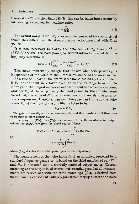
!■!
5.1 Definitions-
temperature Ts is higher than 288 °K, this can be taken into account by- introducing a so-called temperature ratio:
T8(78)a = 288’
The actual noise factor Na of an amplifier preceded by such a signal source thus differs from the standard noise factor measured with Rs at 288 °K.
It is now necessary to clarify the definition of Pm\ Since d£2 = 4kTRs6f, the available noise power, considered within an element d/of the frequency spectrum, is:
d Pni = d
=
4 k TRsdf = kTdf.
This shows, remarkably enough, that the available noise power Pni is independent of the value of the internal resistance of the noise source.
As a rule only part of the entire spectrum is passed by the amplifier. If P„i at the input were taken over the frequency range from zero to infinity and the integration carried out over the entire frequency spectrum, while for P1l0 at the output only the band passed by the amplifier were considered, the value of N thus obtained would obviously give an erroneous impression. Therefore, denoting the pass-band by B„, the noise power P„i at the input of the amplifier is taken to be:
Pni = k T Bn.The gain will usually not be uniform over Bn, and this pass-band will then have
to be defined more accurately.In deriving eq. [11a), Pnf (Gp)s was assumed to be the avaible noise output
originating exclusively from the signal source. Hence:
(79)4 Rs
(80)I
; Ii
-00
. = J* T{Gp)jdf, . IPni{Gp), — k T Bn[GP)
or ni -j£p)/d/. (81)Bn [Gp)s
;where [Gp)f denotes the avaible power gain at the frequency /.
The measurement of the noise factor N of an amplifier, preceded by a standard frequency generator, is based on the third member of eq. (77a) and P1l0 is measured with a correctly matched output meter. (Correct matching at the output is, of course, not essential provided all measurements are carried out with the same matching.) (Gp)s is derived from measurements carried out with a signal which largely exceeds the noise
i
■
II61
■
..:
Noise 5
level Pni as defined by eq. (80). Bn follows according to eq. (81) from a response curve, bearing in mind that Gp is proportional to the square of the voltage gain G. Since the noise temperature Ts of the standard signal generator usually differs from 288 °K, this measurement gives:
P nok TsBn {Gp)s
Na = (82)
k being 1.37 * 10-23 joule /°K. If the noise temperature of the standard signal generator is Ts = 288 °K the actual noise factor iVa is equal to the standard noise factor Nst. As mentioned above, the noise temperature Ts of the standard signal generator usually differs from 288 °K, i.e. 7's/2S8 = a, in which case Nst is calculated from the measured values as follows:
Pno — {Gp)s ft TsBn -f- (Gp)s ft 288BnNst =
{Gp)s ft 288 B„or
P no (83)Nst = -f- 1 — a.{Gp)s ft 288 Bn
Denoting the first term in the second member of eq. (83), which strongly resembles eq. (82), by Nm, this gives:
(83a)Nst = Nm + 1 — a.Thus Nm is a fictitious noise factor obtained when calculations are carried out
according to eq. (82) and Ts is assumed to be 288 °K. To determine the actual noise factor the true value of Ts must be employed according to the definition of eq. (82), giving:
N mv \t 288 Na — N m•-s,— (82a)
In the above little attention was paid to the inherent noise of the amplifier itself. This is dealt with in detail in the following section, but it will be useful to discuss a few related conceptions here.
On page 60 eq. (77a) led to a definition of N as a ratio of noise powers at the output of the amplifier, but N can also be considered as the ratio of P,iol(Gp)s to Pni, i.e. of available powers at the signal source. P«0/(Gp)s then consists of a part Pni originating from the signal source and a part Pnr which represents the equivalent amplifier noise imagined to be located in the signal source. Eq. (77a) then becomes:
Pni 4“ Pnr _ , . PnrPni ~ + Pni
In this expression Pnr is the equivalent available noise power of the amplifier reflected into the signal source. This again is a figure which depends on the matching between signal source and amplifier.
Ts a
1 1
.:
I(775)N =
62
5.2 Calculation of the noise factor 5.2.1
A different method of expressing the inherent noise (for frequencies at which no induced grid noise occurs) has long been employed for amplifying valves, where the concept of equivalent noise resistance Rcq is used, i.e. a fictitious resistance at room temperature connected in series with the grid. The actual noise causes are then imagined to be absent, but Rcq is assumed to have a value such that the noise voltage across it gives rise to the same noise as that normally present in the anode circuit.
Similarly, it is often useful to consider the inherent noise of a complete amplifier as originating from an equivalent resistance Rn at its input, but in this case it should be recognized that the value of Rn may depend both on the signal source and on the amplfier.
5.2 CALCULATION OF THE NOISE FACTOR
11 will now be shown how to calculate the noise factor N, for several cases, from the equivalent noise resistance Rn at the input grid of a given amplifier.
5.2.1. Noise factor of an amplifier without input damping
When an amplifier, the input damping g of which is assumed to be zero,is connected direct to a _____ ______signal source with an internal resistance Rs (see fig. 53), the noise factor N can be calculated from the definition given by eq. (11a).
The available noise power at the output Pll0 is directly proportional to Rs -f- Rn at the input.If the inherent noise of the amplifier were absent (Rn = 0), the noise would be directly proportional to Rs. Hence:
Rs + Rn
VtkTBnRs VtkTBnRn<5>Rs—aruumr ki
ESoAS)Esi Eno
f
65626Fig. 53. Equivalent circuit of an amplifier having no input conductance and a definite, equivalent noise resistance Rn, connected to a signal generator with
a noise resistance R$ and a noise temperature T. i
Rn (84)N = -1 + 3TRs
If the temperature ratio of the signal source is a, its noise power must be multiplied by a and the actual noise factor obviously becomes:
(84a)Na =
By rewriting eq. (84) as:(845)Rs -p Rn — RRs,
63
L
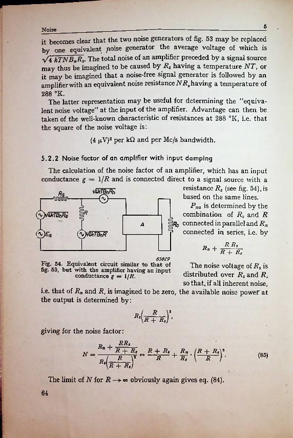
f5Noise
it becomes clear that the two noise generators of fig. 53 may be replaced by one equivalent noise generator the average voltage of which is VTkTNBnRs. The total noise of an amplifier preceded by a signal source may thus be imagined to be caused by Rs having a temperature NT, or it may be imagined that a noise-free signal generator is followed by an
plifierwith an equivalent noise resistance NR8 having a temperature of 288 °K.
The latter representation may be useful for determining the "equivalent noise voltage" at the input of the amplifier. Advantage can then be taken of the well-known characteristic of resistances at 288 °K, i.e. that the square of the noise voltage is:
(4 |j.V)2 per kQ and per Mc/s bandwidth.
am
5.2.2 Noise factor of an amplifier with input damping
The calculation of the noise factor of an amplifier, which has an input conductance g = l/R and is connected direct to a signal source with a
resistance Rs (see fig. 54), is based on the same lines.
P»o is determined by the combination of Rs and R connected in parallel and Rn connected in series, i.e. by
Wffim©^y/AkTBnRs
A%W4kTBnR'
R RsRn + R + R$65629
Fig. 54. Equivalent circuit similar to that of fig. 53, but with the amplifier having an input
conductance g = l/R.The noise voltage of Rs is
distributed over Rs and R, so that, if all inherent noise,
i.e. that of Rn and R, is imagined to be zero, the available noise power at the output is determined by:
giving for the noise factor:
RRSRn + R -f- Rs R -f- RsN = (85)( R y - R \R + Rs)R•
.3.* The limit of N for R oo obviously again gives eq. (84).
64
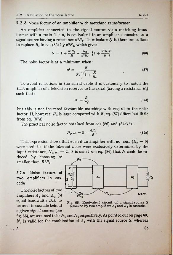
5.2.35.2 Calculation of the noise factor
5.2.3 Noise factor of an amplifier with matching transformer
An amplifier connected to the signal source via a matching transformer with a ratio 1 : n, is equivalent to an amplifier connected to a signal source having a resistance n2Rs. To calculate N it therefore suffices to replace Rs in eq. (85) by n2Rs, which gives:
l+~iT + n*R8 \l + ~~FT)
The noise factor is at a minimum when:
.
(86)N =
Rn* = (87)
^]A + #nTo avoid reflections in the aerial cable it is customary to match the
H.F. amplifier of a television receiver to the aerial (having a resistance Rs) such that:
o R71- = — (8? a)Rs'
but this is not the most favourable matching with regard to the noise factor. If, however, Rn is large compared with R, eq. (87) differs but little from eq. (87a).
The practical noise factor obtained from eqs (86) and (87a) is:
\r o iApract — 2 -j----
This expression shows that even if an amplifier with no noise (Rn = 0) were used, i.e. if the inherent noise were exclusively determined by the input resistance, iVpract = 2. It is seen from eq. (86) that N could be reduced by choosing n2 smaller than R/Rs-
.
(86a)
.Pnrf
5.2.4 Noise factors of two amplifiers in cas- s cade
The noise factors of two amplifiers Ax and A2 (of equal bandwidth Bn), to be used in cascade behind a given signal source (see fig. 55), are assumed to be Nx and N2 respectively. As pointed out on page 60, Nx is valid for the combination of Ax with the signal source S, whereas
PoiAj A2
X.'4? & 65030nrj
Fig. 55. Equivalent circuit of a signal source 5 followed by two amplifiers A x and A 2 in cascade.
65- 5
Noise 5
N2 is valid for A2 connected to a signal source having the same impedance as the output of Ax.
The value of the total noise factor N of two amplifiers connected in cascade, expressed in Nx and N2, will now be investigated. First the inherent noise of A2 is reflected into the input of the amplifier as an available noise power P„r2 originating from the output of Av (This explains why No has been defined as above.)
If the noise factor behind a signal source with an available noise power P„i is No, then, according to eq. (77b):
\t — 1 .iv2 — i -t- ,/u
whence:Pm* — (No— 1) Pni-
(Since, in defining Nx and N2, the noise temperature of the signal source and the bandwidth were assumed to be identical, Pni at the input of A and Pt,i of the signal source are identical; see eq. (80).)
It is now possible to go a step further by imagining Pur2 to originate from the signal source, as an available noise power which now is l/[Gp)1 times P„r2. The inherent noise power of A2, reflected into the signal source, is therefore:
2
(N2 — 1) Pni (88)(Gp)i
Similarly, the inherent noise power of Ax can also be reflected into the signal source, its value then being:
(89)Pnr\ — (Ni — 1) Pni•
The inherent noise of the total circuit connected in cascade, reflected into the signal source Pnr, is obviously equal to the sum of eqs (88) and (89). Calculating the total noise factor N from eq. (77b), gives:
1 + —- = 1+ — * ^ + Pni + Pni <(No—1) PniN =
(Gp) iHence:
N = N, 4- N°-~~ l.1 + (Gph
If the noise factor of the second stage is of the same order as that of the first stage following the signal source (the aerial), the noise contribution of the second stage is obviously negligibly small compared with the total noise, provided the power gain (Gp)1 of the first stage is large.
In deducing eq. (90), the matching of Ax to the signal source need not be
(90)
66
:
I
f5.3 Causes of noise in a valve 5.3.1
considered. It should be noted, however, that incorrect matching is necessarily accompanied by a decrease of (Gp)v In other words, incorrect matching to the aerial increases the noise contribution of A2.
5.3 CAUSES OF NOISE IN A VALVE
In the previous sections the inherent noise of an amplifier was represented bj' an equivalent noise resistance Rn or by a reflected noise power Pnrt without specifying the actual causes of this noise.
The amplifying valves contribute largely towards this noise and this contribution consists, in turn, of various components, each having its own origin in the valve considered.
It is very important to note that the magnitude of some of these components depends on the frequency and it is therefore obvious that these cannot be imagined to originate from an equivalent noise resistance. In fact, if the inherent noise of a valve is expressed in the customary way by the equivalent noise resistance i?eq (see page 63), only the components which are independent of the frequency are inferred, and at frequencies below 30 Mc/s these are indeed practically the only sources of noise.
The following are the principal causes of noise in a valve.
!
:
l!
i5.3.1 Emission and partition noise
In the simplest type of valve, i.e. the diode, the shot effect of the emission is the only source of noise. In the case of a saturated diode the mean square of the noise component in the emission current, measured within a frequency band Bn, is:
!'
(91)J«2 = 2 elk Bn,
in which Ik denotes the cathode current.When the emission current is not at saturation value the space-charge
effect reduces the noise by the factor Fk, called the space-charge attenuation factor, giving:
(91a)Ic- = 2 Fk2 e Ik Bn.
This emission noise is also present in all valves containing one or several grids and can be expressed1) in terms of the cathode temperature 7* and S', the so-called transconductance for the effective control voltage, so that eq. (91«) becomes: i
Ic2 = 0.64 {4k Tk S' Bn).q C. J. Bakker, The Causes of Voltage and Current Fluctuations, Philips
Techn. Review 6, p. 129, 1941 (No. 5).
(915)■
67
Noise 5
From eqs (91a) and (916):
0.64 • 4 kTk S'Fir = (92)2 e Ik
The transconductance S' is usually about 1 to 2 times the normal mutual conductance and Tk is approximately equal to 3.5 times the room temperature; hence Fk2 lies between 0.1 S/Ik and 0.2 S/I*. For most cases a good approximation is:
Fk2 « 0.125 • (92a)TkThere is a striking resemblance between eq. (916) and the expression for the
Johnson noise in a resistance, viz.:
-p_ En2_ 4& TR Bn 4& T Bn1 ~w ~ w (91c)RClearly 1/S' in eq. (916) plays the same part as R in eq. (91c).
In addition to the emission noise the irregularity of the “partition” of the current between anode and screen grid also comes into play in multigrid valves. The so-called partition noise thereby caused is given by the expression :
2e • IfLllV = (93)1 * Bn — 2FpzeI(tBn,
from which the partition noise factor is:
hi (93 a)
The emission and partition noise currents are obviously manifest in the anode circuit. The emission noise has been shown to be proportional to the cathode current Ik, whereas the partition noise is proportional to the anode current Ia. If, to a first approximation, Ia is assumed to be equal to Ik in tetrodes and pentodes, and the two noise currents in the anode circuit are added, then:
(Ie+py-=2Fa*eIaBn,
in which, according to eqs (91a) and (93):
Fa* * Fk2 + FPZ.
(94)
(95)
The equivalent noise resistance Rcq is now considered as the cause of the noise current (Ie+P)2 according to eq. (94), and can therefore be calculated from:
4 kTB Rcq S2 = 2 Fa2 e Ia B,
68
i
IL
5.3 Causes of noise in a valve 5.3.2
which gives J):
Rcq can further be imagined to be composed of two resistances, one of which is responsible for the emission noise, and the other responsible for the partition noise. When the latter resistance is denoted by Rp, it is obvious that:
Fa2 laReq “ 2kT S2 (96)
Rp FP2 1 (97)-??eq Fp2 Fk2 Fk2 1 4- — ^ Fp2
This quotient will be denoted by K3.A simple approximation for Req is obtained by substitution of eq. (95)
in eq. (96) after eqs (92a) and (93«) have been substituted in eq. (95), viz.:
*.q *rt'(¥ + 20 ■ §5)(kn)-
From this formula it will be clear that:
(96a)
Ig2 laIkS2’
(98)Rp fa 20 •
and1 (99)K„fa3
1 + 8/Ja ;
The following sections will show the advantage gained by splitting Req into Rp and (RQq — Rp). As a rule, only Rcq is quoted in valve data. !
:i
!5.3.2 Induced grid noise
Owing to the finite transit time of the electrons the following effects occur:(a) In a direct connection between the control grid and cathode addi
tional fluctuations are induced, the values of which are given by:
(100)
:■
■■
■
I:
1
Ig2 = constant • TkS B*©*^*,
where denotes the transit time from cathode to control grid. (6) The input circuit is subject to an additional damping gT, viz.:
gx = constant • Sco2 Tkg2.
'
(101) t
*) The charge of the electron e = 1.6 x 10~18 coulomb and k = 1.37 X 10⁻²³ . joule/°K.
69 •••
.:.'
Noise 5
As shown in the literature referred to above, the fluctuations Is2 may be interpreted as the noise of the resistance Rr = 1 /gx if the temperature is taken to be equal to about 1.43 7* = aT288, a- being about 5, and assuming that there is no coherence between emission noise and induced grid noise.
This assumption is permissible here because, although there is coherence between these two kinds of noise and a possibility of noise compensation is thereby offered, such a compensation is difficult to achieve in practice. This possibility may therefore be disregarded and the more simple formulae which neglect coherence are used in this book, the slight improvement of N which might be obtained within a limited frequency range not being considered. This improvement may be expected to be less than 3 db.
'
;
5.4 CALCULATION OF THE NOISE FACTOR AT METRIC WAVES
5.4.1 General equations
The signal-to-noise ratio may undergo considerable changes due to feedback. At very high frequencies the self-inductance of the cathode lead gives rise to an additional input damping which reduces the signal strength. The noise in the input circuit (including the valve damping) is, however, also decreased by this damping and the same applies to the emission noise, which is reduced in the same proportion as the signal by the feedback in the cathode lead. The partition noise current, on the other hand, does not flow through the feedback circuit and remains unchanged.
Emission and partition noise are combined in the concept of “equivalent noise resistance”, but since the feedback damping affects the emission noise and the partition noise differently^, it is desirable to make a distinction between the two. For this reason, in addition to the equivalent noise resistance Rcq, the concept of “partition noise resistance” Rp has been introduced in Section 5.3.1, viz.:
r
;'
i
Rp\pRp (102)
Since the fictitious resistance Rt across the input, representing the damping caused by the cathode lead inductance, can be proved to produce no additional noise *), the equivalent is as shown in fig. 56.
M. J. O. Strutt and A. van der Ziel, The Noise in Receiving Sets at Very High Frequencies, Philips Techn. Review 6, p. 178, 1941 (No. 6).
70
!
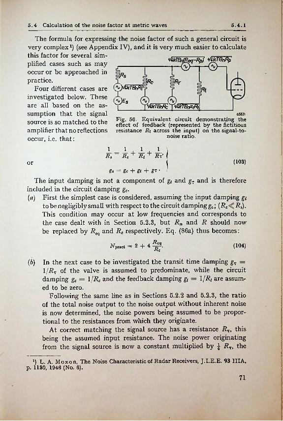
5.4 Calculation of the noise factor at metric waves 5.4.1
The formula for expressing the noise factor of such a general circuit is very complex1) (see Appendix IV), and it is very much easier to calculate this factor for several simplified cases such as may occur or be approached in practice.
Four different cases are investigated below. These are all based on the assumption that the signal source is so matched to the
V4kT8n(Req-Rp) V4kTBnRp
!*s\Rc \Rr
^MkTBnRi
'V/y)Es 'VV4kTBnR:JV4kTBnaA
I65831Fig. 56. Equivalent circuit demonstrating the effect of feedback (represented by the fictitious
amplifier that no reflections resistance Rt across the input) on the signal-to-noise ratio.occur, i.e. that:
1 1 l l !Rs Rc+ Rt+ Rt’(103)or
gs = gc + gt + g* •The input damping is not a component of gt and gx and is therefore
included in the circuit damping gc.(a) First the simplest case is considered, assuming the input damping gi
to be negligibly small with respect to the circuit damping gc; (7?c Rt). This condition may occur at low frequencies and corresponds to the case dealt with in Section 5.2.3, but Rn and R should now be replaced by Rcq and Rc respectively: Eq. (86a) thus becomes:
2 + 4tr- (104)Npract —
(6) In the next case to be investigated the transit time damping gx = l/R- of the valve is assumed to predominate, while the circuit damping gc = 1 /Rc and the feedback damping gt = l/Rt are assumed to be zero.
Following the same line as in Sections 5.2.2 and 5.2.3, the ratio of the total noise output to the noise output without inherent noise is now determined, the noise powers being assumed to be proportional to the resistances from which they originate.
At correct matching the signal source has a resistance Rx, this being the assumed input resistance. The noise power originating from the signal source is now a constant multiplied by £ Rx> the
q L. A. Moxon, The Noise Characteristic of Radar Receivers, J.I.E.E. 93 IIIA, p. 1130, 1946 (No. 6).
71
Noise 5
factor £ accounting for the signal source being loaded by a resistance of the same value as the internal resistance.
The noise contribution of the transit time resistance is equal to the product of the same constant and £ aZRX, in which the factor £ now accounts for the load of R- by the signal source and aT having the meaning given in Section 5.3.2.
Finally, the unloaded resistance Rcq contributes towards the noise, so that the total noise originates from a resistance:
i R-z + £ d" ^eq,giving for the noise factor:
£ Rt + £ aT^T + -fteq R cq (105)Npract — = 1 + «t+4^.
(c) Whereas in the previous case only gT of the input conductance was taken into account, the case where only the feedback conductance gt is present will now be investigated. The circuit conductance gc = 1/RC is again assumed to be zero, and the resistance of the signal source is Rt.
The noise from the signal source is now directly proportional to £ Rt. Of the total valve noise the partition noise must be taken fully into account, so that this noise contribution is proportional to Rp. The noise contribution from (Rcq — Rp), on the other hand, is distributed over the resistance of the signal source and the resistance Rt. Since these two resistances are assumed to have the same value, only £ of the square of this noise voltage is operative in the amplifier.
The total noise power is therefore determined by:Rt + Rp + £ (^cq — Rp)>
giving for the noise factor:
AW - * * + + * (*°q ~ Rp) = 1 + 3 g?
(d) Finally, the two preceding cases will be combined, but for the sake of simplicity Rx is assumed to be equal to Rt, while Rx and Rt connected in parallel will now be denoted by Ri. The circuit conductance gc = 1JRC is again assumed to be zero (cf. fig. 56).
The noise originating from the signal source is now determined by £ Ri, while the partition noise is determined by Rp. The source of the transit time noise, i.e. in first instance a^RXt is loaded by Ri connected in parallel with 2Ri, that is to say by f Ri, and its internal
. ^£3 ^ Rt' (106)
72
5.4 Calculation of the noise factor at metric waves 5.4.1
resistance is Rx = 2R{. The transit time noise power is thus given by:
iM- :«t Rr = £ aT Ri-«T#T * (107)
The equivalent voltage of the emission noise originating from (Req — Rp) is distributed over Rt and the parallel connection of Rt and Rlt i.e. over 2 R{ and f R{. This noise power is thus given by:
(i?cq--Rp) QiJ — (^cq — Rp)> (108)
giving for the noise factor:
Npract =:}• Ri + Rp + 1 a-i?t -f- (-^cq — Rp)
YRi
In the four cases investigated the matching of the signal source to the amplifier was assumed to be such that no reflection occurs. As shown in Section 5.2.3, matching may, however, be such that N is a minimum. For the calculation of this matching and of the values of 2Vopt obtained in that case, reference is made to Appendix IV.
Apart from case (a), which applies to low frequencies only, there appear to be but three quantities on which the noise factor depends, viz.:
a constant « 5,Rcq/Ri, a quantity which depends only on the frequency and is a valve
quantity J),Rp/Ri, which can be expressed in terms of Rcq by means of the factor
Kz = Rp/Rcq. For triodes I<3 is obviously zero, while for pentodes I/A3 » 1 + S/Sig2, Kz tending towards unity when the partition noise predominates, and being about £ in the case of high-slope pentodes.
Because of the term Ri the quantity Rcq/Ri is proportional to the square of the frequency, viz.:
IRp Rcq
= l+i«T-Mfl7+ ^~Ri' (109)
aT
^cq _ ity Ri “ \fn) ' (110)
where fn is the noise reference frequency at which Rcq/Ri = Rcq • gi is unity.
Taking these considerations into account, the special cases mentioned
J) It is true that Ri depends on the amount of feedback by the cathode lead, but the limit to which this effect can be reduced in practice may also be regarded as a valve characteristic.
73
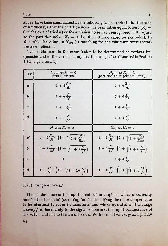
Noise 5
above have been summarized in the following table in which, for the sake of simplicity, either the partition noise has been taken equal to zero (K3 =0 in the case of triodes) or the emission noise has been ignored with regard to the partition noise (/C3 = 1, i.e. the extreme value for pentodes). In this table the values of iVopt (at matching for the minimum noise factor) are also indicated.
This table permits the noise factor to be determined at various frequencies and in the various ‘'amplification ranges” as discussed in Section1 (cf. figs 3 and 5).
Npract at — 0 (triode circuit)
Nprnct at K3 — 1(partition noise predominating)Case
2 + 4^3Hc
6 + 4 -£r
2 + 4^3He
a
r-b 6 + 4-K-f>r fn-
r- *c 1 + 1 + 4fn2 hr
r- rd l + 4-fr3 + fn2 /«2
Nopt at Kz = 0 ■^'opt at /q — 1
1 + +
1 + '-fr'(1 + yi + *-r)l + 2^-(a' 1 +R
1 + 2-&-(1 + ]A + 5f)b'
r-c’ 1 + 4 4^-1 hr
l + 2ir(1 + ]h + 'If)1 + Ji7'{l + ]h + loIf)d'
5.4.2 Range above f0'
The conductance of the input circuit of an amplifier which is correctty matched to the aerial (assuming for the time being the noise temperature to be identical to room temperature) and which operates in the range above f0' is due mainly to the signal source and the input conductance of the valve, and not to the circuit losses. With normal valves gt and gT may
74
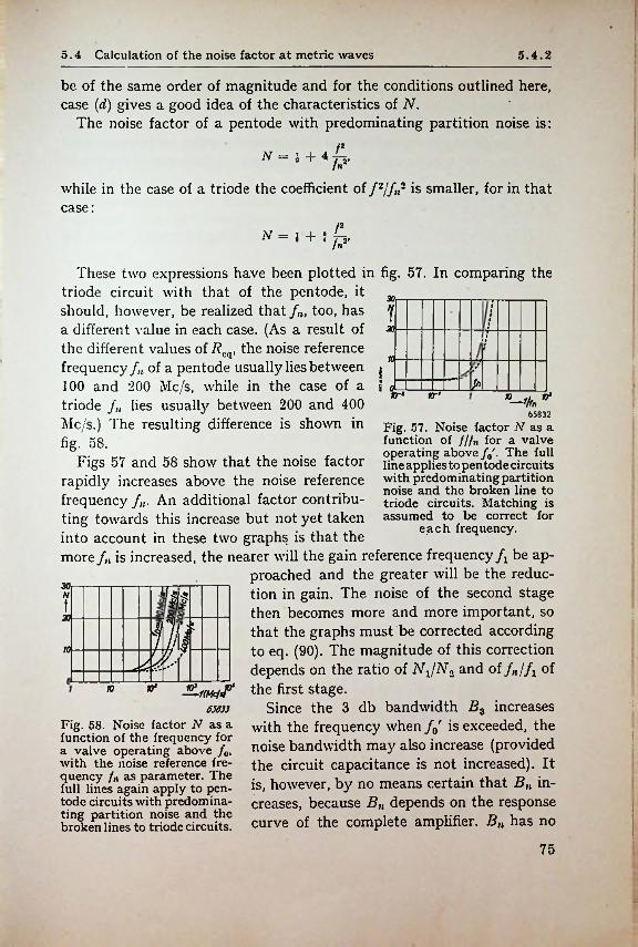
5.4 Calculation of the noise factor at metric waves 5.4.2
be of the same order of magnitude and for the conditions outlined here, case (d) gives a good idea of the characteristics of N.
The noise factor of a pentode with predominating partition noise is:
3 + fnV
while in the case of a triode the coefficient of /2//«2 is smaller, for in that case:
N =
r~N = l + '< fsUV
These two expressions have been plotted in fig. 57. In comparing the triode circuit with that of the pentode, it xshould, however, be realized that /„, too, has ^a different value in each case. (As a result of i
:the different values of R,.n, the noise reference frequency fn of a pentode usually lies between j 100 and 200 Mc/s, while in the case of a i ct triode f„ lies usually between 200 and 400 Mc/s.) The resulting difference is shown in fig. 58.
7v>
KT'"-f/fn *
65832Fig. 57. Noise factor N as a function of ///» for a valve
bigs 57 and 58 show that the noise factor line appliesto pentode circuitsrapidly increases above the noise reference with predominating partition . . .... noise and the broken line tofrequency fn. An additional factor contributing towards this increase but not yet taken into account in these two graphs is that the more fn is increased, the nearer will the gain reference frequency fx be ap
proached and the greater will be the reduction in gain. The noise of the second stage then becomes more and more important, so that the graphs must be corrected according to eq. (90). The magnitude of this correction depends on the ratio of NJN2 and of fn/fi of the first stage.
Since the 3 db bandwidth Bz increases with the frequency when /0' is exceeded, the noise bandwidth may also increase (provided the circuit capacitance is not increased). It is, however, by no means certain that Bn increases, because Bn depends on the response curve of the complete amplifier. Bn has no
triode circuits. Matching is assumed to be correct for
each frequency.
30ill <»N mi !20 m10
65633Fig. 58. Noise factor N as a function of the frequency for a valve operating above /„, with the noise reference frequency fn as parameter. The full lines again apply to pentode circuits with predominating partition noise and the broken lines to triode circuits.
10
75
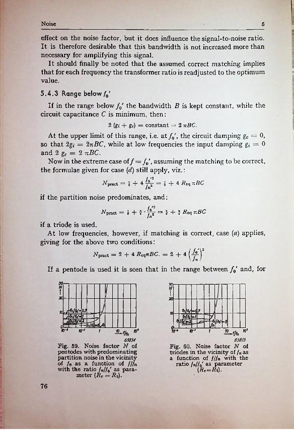
Noise 5
effect on the noise factor, but it does influence the signal-to-noise ratio. It is therefore desirable that this bandwidth is not increased more than necessary for amplifying this signal.
It should finally be noted that the assumed correct matching implies that for each frequency the transformer ratio is readjusted to the optimum value.
5.4.3 Range below f0'
If in the range below /0' the bandwidth B is kept constant, while the circuit capacitance C is minimum, then:
2 (gi -f- gc) = constant = 2 tzBC.At the upper limit of this range, i.e. at /0', the circuit damping gc = 0,
so that 2gi = 27zBC, while at low frequencies the input damping gi = 0 and 2 gc = 2 -BC.
Now in the extreme case of/ = /0', assuming the matching to be correct, the formulae given for case (d) still apply, viz.:
Npract =3 + ^ = i + ^ Rcq —BC
if the partition noise predominates, and:
Npract = i + % ’ — l + ? 7?Cq BC
i
if a triode is used.At low frequencies, however, if matching is correct, case (a) applies,
giving for the above two conditions:
Npract = 2 —f— 4 RcqjzBC. = 2 4
If a pentode is used it is seen that in the range between /0' and, form
30N NI
20
fn fa = ( 7fnlfti =1 “ ItAh/to’* 1
fnft ffo' =2fnlfo'm 2
=5LA o'— 10-* *>" 1 2Uf/fn *
65635Fig. 60. Noise factor N of triodes in the vicinity of fn as a function of ///» with the
ratio fn/fo as parameter (Rx=Rt).
10-* w ^f/fn 103 65634
Fig. 59. Noise factor N of pentodes with predominating partition noise in the vicinity of fn as a function of ///« with the ratio /«//„' as para
meter {Rr = Ri).3
76I
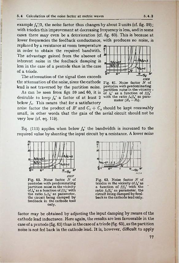
5.4 Calculation of the noise factor at metric waves 5.4.3
example /0'/3, the noise factor thus changes by about 2 units (cf. fig. 59); with triodes this improvement at decreasing frequency is less, and in some cases there may even be a deterioration (cf. fig. 60). This is because at lower frequencies the feedback conductance, with produces no noise, is replaced by a resistance at room temperature so- in order to obtain the required bandwith. ^The advantage gained from the absence of 20' inherent noise in the feedback damping is n less in the case of a pentode than in the case of a triode.
fyf0'= !1
fn f0'f5lo-1 -2-0br
65636the attenuation of the noise, since the cathode Fig. 61. Noise factor N oflead is not traversed by the partition noise, pentodes with predominating
. err . . . partition noise in the vicinity >As can be seen from figs 59 and 60, it is Qf /„' as a function of ///„'
desirable to keep L' a factor of at least 2 with the ratio /«//0'as para-below /„. Phis means that for a satisfactorynoise factor the product of B' and Ct + Cx should be kept reasonably small, in other words that the gain of the aerial circuit should not be
The attenuation of the signal then exceeds
!
very low (cf. eq. 116).
Eq. (Ill) applies when below f0' the bandwidth is increased to the required value by shunting the input circuit by a resistance. A lower noise
30N N I! i20
IJ
fhjf^ 12 w-*nIfo..07 12\5
102«oW
Fig. 63. Noise factor N of triodes in the vicinity of /„' as a function of ///„' with the ratio fn/fo as parameter, the circuit being damped by feedback in the cathode lead only.
i2-4* "*
65637Fig. 62. Noise factor N of pentodes with predominating partition noise in the vicinity of as a function of ///„' with the ratio /„//„' as parameter, the circuit being damped by feedback in the cathode lead
only.
factor may be obtained by adjusting the input damping by means of the cathode lead inductance. Here again, the results are less favourable in the case of a pentode (fig. 62) than in the case of a triode (fig. 63), as the partition noise is not fed back in the cathode lead. It is, however, difficult to apply
w3 nt4 r1
77
i
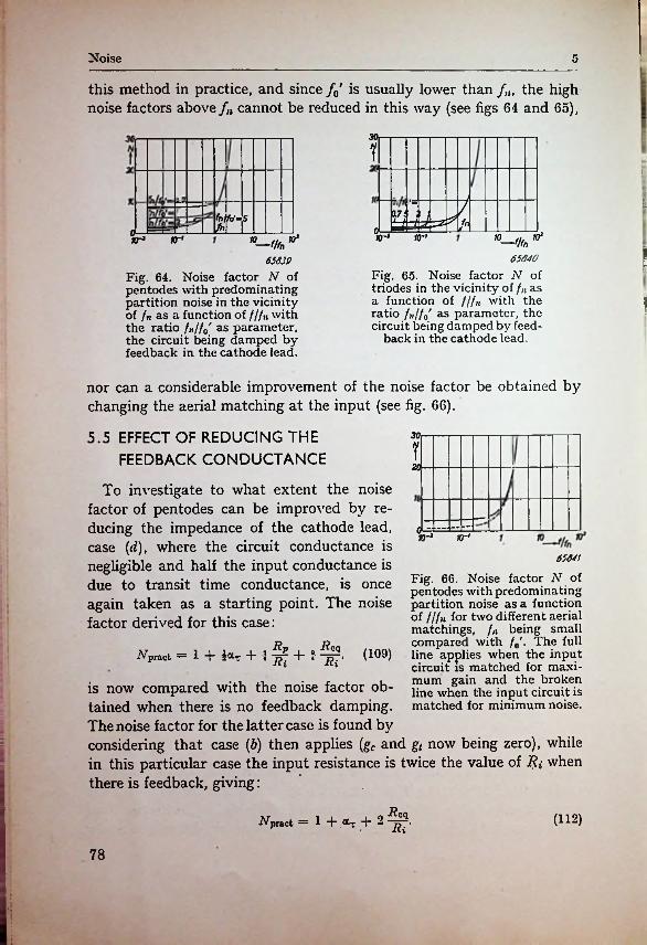
Noise 5
this method in practice, and since /0' is usually lower than /,„ the high noise factors above /„ cannot be reduced in this way (see figs 64 and 65),
30ri
H—1175fit1 ikt* vFnr3 tr'
65640
Fig. 65. Noise factor iV of triodes in the vicinity of /„ as a function of ///» with the ratio /n//0' as parameter, the circuit being damped by feed
back in the cathode lead.
1°-f/fn 10165639
Fig. 64. Noise factor N of pentodes with predominating partition noise in the vicinity of fn as a function of fffn with the ratio f„lf0' as parameter, the circuit being damped by feedback in the cathode lead.
C|
nor can a considerable improvement of the noise factor be obtained by changing the aerial matching at the input (see fig. 66).
5.5 EFFECT OF REDUCING THE FEEDBACK CONDUCTANCE
30r20
To investigate to what extent the noise factor of pentodes can be improved by reducing the impedance of the cathode lead, case (d), where the circuit conductance is negligible and half the input conductance is due to transit time conductance, is once
10-> J0-'
65641
Fig. 66. Noise factor N of pentodes with predominating
again taken as a starting point. The noise partition noise as a functionfactor derived for this case: Si
compared with /„'. The full (109) line applies when the input
circuit is matched for maximum gain and the broken line when the input circuit is
tained when there is no feedback damping, matched for minimum noise.
Npract = 1 + 4a- + J ■— + ? -^7,
is now compared with the noise factor ob-
The noise factor for the latter case is found byconsidering that case (b) then applies (gc and gt now being zero), while in this particular case the input resistance is twice the value of Ri when there is feedback, giving:
:
Npract = 1 + .®r + 2 -^7. (112)
78
j
'
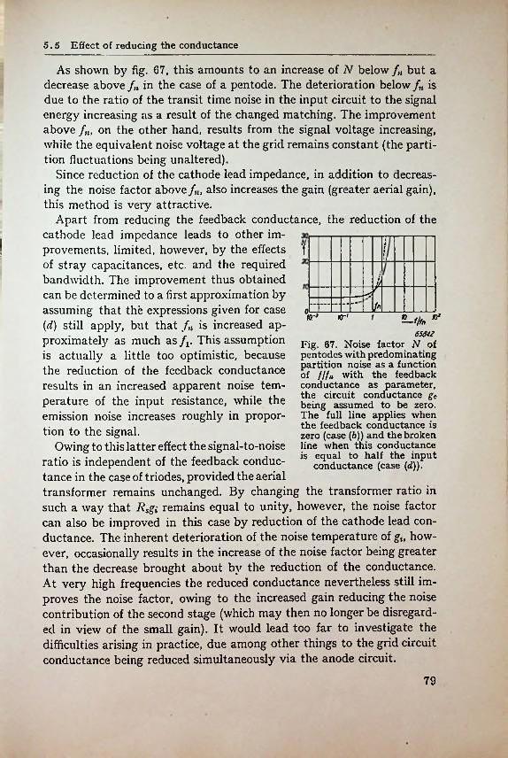
5.5 Effect of reducing the conductance
As shown by fig. 67, this amounts to an increase of N below /„ but a decrease above /„ in the case of a pentode. The deterioration below fn is due to the ratio of the transit time noise in the input circuit to the signal energy increasing as a result of the changed matching. The improvement above /„, on the other hand, results from the signal voltage increasing, while the equivalent noise voltage at the grid remains constant (the partition fluctuations being unaltered).
Since reduction of the cathode lead impedance, in addition to decreasing the noise factor above/„, also increases the gain (greater aerial gain), this method is very attractive.
Apart from reducing the feedback conductance, the reduction of the cathode lead impedance leads to other improvements, limited, however, by the effects of stray capacitances, etc. and the required bandwidth. The improvement thus obtained can be determined to a first approximation by assuming that the expressions given for case (d) still apply, but that /„ is increased approximately as much as fv This assumption is actually a little too optimistic, because the reduction of the feedback conductance results in an increased apparent noise temperature of the input resistance, while the emission noise increases roughly in proportion to the signal.
Owing to this latter effect the signal-to-noise ratio is independent of the feedback conductance in the case of triodes, provided the aerial transformer remains unchanged. By changing the transformer ratio in such a way that Rsgi remains equal to unity, however, the noise factor can also be improved in this case by reduction of the cathode lead conductance. The inherent deterioration of the noise temperature of gt, however, occasionally results in the increase of the noise factor being greater than the decrease brought about by the reduction of the conductance. At very high frequencies the reduced conductance nevertheless still improves the noise factor, owing to the increased gain reducing the noise contribution of the second stage (which may then no longer be disregarded in view of the small gain). It would lead too far to investigate the difficulties arising in practice, due among other things to the grid circuit conductance being reduced simultaneously via the anode circuit.
Ii t
J£O'—----——
nr3 n-’ *65642
Fig. 67. Noise factor N of pentodes with predominating partition noise as a function of f/fn with the feedback conductance as parameter, the circuit conductance gc being assumed to be zero. The full line applies when the feedback conductance is zero (case (6)) and the broken line when this conductance is equal to half the input
conductance (case (rf)).
79
Noise 5
Summarizing, it can be stated that the noise factor rapidly increases above /„ and, apart from improving gv, little can be done to counteract this effect.
5.6 CALCULATION OF THE SIGNAL-TO-NOISE RATIO FROM THE NOISE FACTOR
In order to derive the signal-to-noise ratio from the noise factor it should in the first place be taken into account that so far only the standard
noise factor has been considered, i.e. the noise factor of an amplifier following a signal source, the noise temperature of which is equal to room temperature.
At metric waves the noise temperature Ta of an aerial largely depends on the frequency and direction, owing to the contribution of the cosmic noise 2) to the noise level of the aerial. At, say, 40 Mc/s the noise temperature of the aerial may vary for example between 5000 °K and 25,000 °K.
At higher frequencies, however, the noise temperature decreases and at the highest frequencies tends towards the absolute zero point. A calculation of the effect of
the cosmic noise by means of eq. (82a) shows that, at frequencies below 100 Mc/s, Na lies considerably below N; see figs 58 and 68.
Owing to the influence of Ta, valve differences (differing /„ values) have a smaller effect on Na than on N. The noise output of a receiver is now given by:
30
fNat sS
5j
Jt'& F W66022
Fig. 68. Minimum value of the aerial noise factor Na at correct matching as a function of the frequency, with fn as parameter* The full lines apply to pentodes with predominating partition noise and the broken lines to
triodes, both in case (d).
10
Pno = Nak Ta Bn{Gp)s = {N — 1 + a) 288 k Bn{GP)s,
while the signal output is:
H2 x2• (GP)s,Pso = 4jz2 i?rad
where H is the field strength in V/m and X the wavelength in m. The signal- to-noise (power) ratio at the output is thus:
__________H2 x2_________Pno 4:TZ2 (N—1 -{- a) (288 kBnPrad)P*o (113)
J) See the paper by Bakker quoted in footnote on page 67.
80
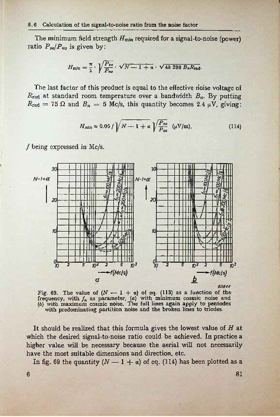
5.6 Calculation of the signal-to-noise ratio from the noise factor
The minimum field strength Hmin required for a signal-to-noise (power) ratio PsolPno is given by:
= l ■ • Vw — 1 + a • Vik 288 B„i?rod.Hmln
The last factor of this product is equal to the effective noise voltage of Rrad at standard room temperature over a bandwidth Bn. By putting •Rrad = 75 Q and Bn = 5 Mc/s, this quantity becomes 2.4 pV, giving:
0.05 / j/iV — 1 + a ]/|5 (|*V/m),•ffiuin ~ (114)
/ being expressed in Mc/s.
—►f(Mc/s) —►f(Mc/s)ba
65644Fig. 69. The value of (iV — 1 + a) of eq. (113) as a function of the frequency, with /„ as parameter, (a) with minimum cosmic noise and (b) with maximum cosmic noise. The full lines again apply to pentodes
with predominating partition noise and the broken lines to triodes.
It should be realized that this formula gives the lowest value of H at which the desired signal-to-noise ratio could be achieved. In practice a higher value will be necessary because the aerial will not necessarily have the most suitable dimensions and direction, etc.
In fig. 69 the quantity (N — 1 + a) of eq. (114) has been plotted as a
816
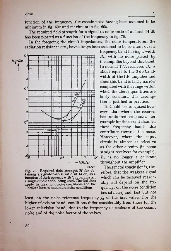
5Noise
function of the frequency, the cosmic noise having been assumed to be minimum in lig. 69« and maximum in fig. 696.
The required field strength for a signal-to-noise ratio of at least 14 db has been plotted as a function of the frequency in fig. 70.
In the foregoing the circuit impedances, the noise temperatures, the radiation resistance etc., have always been assumed to be constant over a
frequency band having a width Bn, with no noise passed by the amplifier beyond this band. In normal T.V. receivers Bn is about equal to the 3 db bandwidth of the I.F. amplifier and since this band is fairly narrow compared with the range within which the above quantities are fairly constant, this assumption is justified in practice.
It should, be recognized however, that where the receiver has undesired responses, for example for the second channel, these frequency bands also contribute towards the noise. Moreover, where the input circuit is almost as selective as the other circuits (in some straight receivers for example),
jq3 Bn is no longer a constant throughout the amplifier.
The general conclusion is, therefore, that the weakest signal which can be received reasonably will depend on the frequency, on the noise condition (aerial noise) and, last but not
least, oh the noise reference frequency fn of the first valve. For the higher television band, conditions differ considerably from those for the lower television band, due to the frequency dependence of the cosmic noise and of the noise factor of the valves.
HffiV/m)
t103
1°10 102f(Mc/s)
65645Fig. 70. Required field strength H for obtaining a signal-to-noise ratio of 14 db, as a function of the frequency with /« as parameter, a single dipole aerial being used. The full lines apply to maxmum noise conditions and the
broken lines to minimum noise conditions.
82
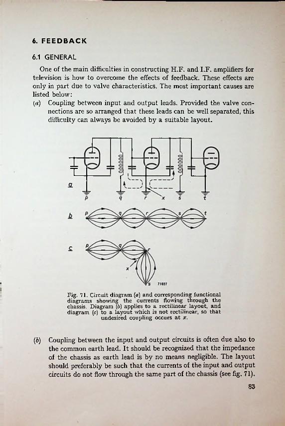
6. FEEDBACK
6.1 GENERALOne of the main difficulties in constructing H.F. and I.F. amplifiers for
television is how to overcome the effects of feedback. These effects are only in part due to valve characteristics. The most important causes are listed below:[a) Coupling between input and output leads. Provided the valve con
nections are so arranged that these leads can be well separated, this difficulty can always be avoided by a suitable layout.
XT
Fig. 71. Circuit diagram (a) and corresponding functional diagrams showing the currents flowing through the chassis. Diagram (6) applies to a rectilinear layout, and diagram (c) to a layout which is not rectilinear, so that
undesired coupling occurs at x.
(6) Coupling between the input and output circuits is often due also to the common earth lead. It should be recognized that the impedance of the chassis as earth lead is by no means negligible. The layout should preferably be such that the currents of the input and output circuits do not flow through the same part of the chassis (see fig. 71).
83
Feedback 6
(c) Feedback of part of the output energy due to the chassis acting as a wave guide. Many different modes are possible, each of which has a definite attenuation per unit length. Long, narrow chassis are usually advisable. A narrow chassis, permitting a high gain per unit length, can be obtained by using valves of small dimensions. The feedback can, moreover, be minimized by providing the chassis with partitions, thereby impeding the passage of guided waves.
(d) Coupling between the stages via the filament lead. This can be avoided by by-passing these connections.
(e) Decoupling faults. Such faults are usually due to the self-inductance of the capacitors and of their connecting leads. Good results are nevertheless obtained when these leads happen to be in series resonance with the capacitor. (For example, when working at 65Mc/s, this will be the case when the inductance of a 200 pF capacitor and its leads is 0.03 (J.H.)
(/) Feedback via the anode-to-grid capacitance. This is the main cause of instability arising from the valves.
(g) Feedback from the cathode circuit to the grid circuit. This effect changes the input conductance and capacitance and, though troublesome in most cases, can sometimes be used to advantage.
(h) Feedback via the anode-to-cathode capacitance. This effect is of particular importance when taking advantage of the effect mentioned under (g) to influence the input admittance of the valve, for which purpose a fairly large impedance is incorporated in the cathode lead.
Only the effects mentioned under (/), (g) and (h) will be discussed in detail. The formulae required are derived for an amplifying stage in which all these three effects are present. The detailed discussion of each form of feedback is confined to a system in which only one of these effects is present.
6.2 BASIC FORMULAE :When considering the gain and bandwidth (see Section 1), use was made
of an idealized amplifying stage in which the valve (with an input voltage Vt across the admittance Yt) functions as a constant-current generator supplying a current I0 = SVi to the output admittance Y0. In order to use this simplified representation when negative or positive feedback is present in the amplifying stage, it is first necessary to determine the values of the quantities S', Y{ and Y0' which are substituted for S, Yt- and Y0 in
I
8 4
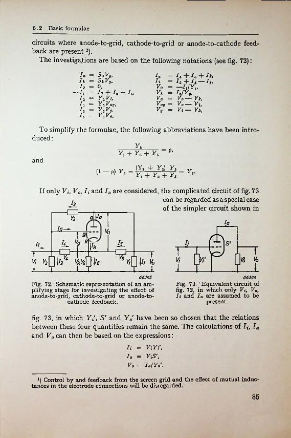
6.2 Basic formulae
circuits where anode-to-grid, cathode-to-grid or anode-to-cathode feedback are presentx).
The investigations are based on the following notations (see fig. 72):
la = SaVg,Ik = SkVg,Ig = 0,
—1\ — la + /3 + 15,12 = y*Vi.13 = YtVag, h = Y*Vg, h = y5Va,
To simplify the formulae, the following abbreviations have been introduced :
h — I\ 4- 15 + Ik, Ii = I2 + I\ — 73,Vo--------IJYVVk = IJYo,Va = Vo — Vk,Vug — Vo— Vi,Vg = Vi— Vk,
y*y, + y, + n Pi
and(Yi + Ya) y5yx + y3 + V,(i - p) y5 = = y7.
If only Y,-, V0, U and Ia are considered, the complicated circuit of fig. 72can be regarded as a special case of the simpler circuit shown inh_
(=] oli^aft lala— Vat 9k. v? k a-4
, Yl
h IiIi \r» TT%n
T T0! Y6 VoViYi y2 Ii Vo\JI i
66395Fig. 72. Schematic representation of an amplifying stage for investigating the effect of anode-to-grid, cathode-to-grid or anode-to-
cathode feedback.
66396Fig. 73.' Equivalent circuit of fig. 72, in which only Vi, V0, Ii and Ia are assumed to be
present.
fig. 73, in which Y/, S' and Yd have been so chosen that the relations between these four quantities remain the same. The calculations of Ii, Ia and V0 can then be based on the expressions:
Ii = ViYY,Ia = ViS', Vo = Ia/Yo
Control by and feedback from the screen grid and the effect of mutual inductances in the electrode connections will be disregarded.
85
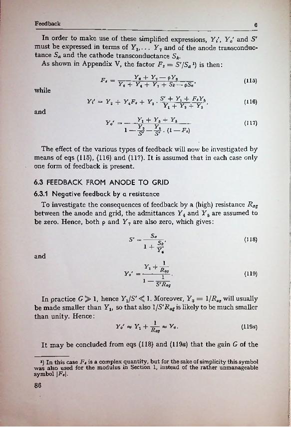
Feedback 6
In order to make use of these simplified expressions, Y/, Yd and S' must be expressed in terms of Ylt... Y1 and of the anode transconductance Sa and the cathode transconductance S*.
As shown in Appendix V, the factor Fs = S'/Sa1) is then:
Y0+ Y7 — pY~3 Y6+ Y4 + Y7 + Sk — pSa’
S' + Y, + FsYs Y1 + Y3 + Yd’
:Fs = (115)
whilefYt' = Y2 + Y*Fs + Y3 • (116)
andYx + Y3 + YsYo = (117)
i Y? Ys /, p \1 s, s, . (1 i«)
The effect of the various types of feedback will now be investigated by means of eqs (115), (116) and (117). It is assumed that in each case only one form of feedback is present.
6.3 FEEDBACK FROM ANODE TO GRID
6.3.1 Negative feedback by a resistanceTo investigate the consequences of feedback by a (high) resistance Rag
between the anode and grid, the admittances Y4 and Y5 are assumed to be zero. Hence, both p and Y7 are also zero, which gives:
S„ (118)5' =Sk’
1 +y- 1 6
andYx + ^-
(119)Y0' =1 S'Rag ■
In practice G > 1, hence YJS' < 1. Moreover, Y3 = 1 /Raa will usually be made smaller than Yv so that also l/S'Rag is likely to be much smaller than unity. Hence:
;
1Yo' « Y, +
It may be concluded from eqs (118) and (119a) that the gain G of the
» y0. (119a)
J) In this case Fs is a complex quantity, but for the sake of simplicity this symbol was also used for the modulus in Section 1, instead of the rather unmanageable symbol |F*|.
86
!!
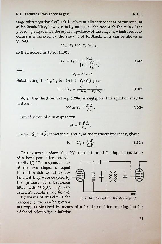
6.3 Feedback from anode to grid 6.3.1
stage with negative feedback is substantially independent of the amount of feedback. This, however, is by no means the case with the gain of the preceding stage, since the input impedance of the stage in which feedback occurs is influenced by the amount of feedback. This can be shown as follows:
S'> Yx and Yl > Y3>
so that, according to eq. (116):Y3S' (120)Yi' = Y, -f
sinceYt + S' « S'.
Substituting 1—Y3/Y1 for 1/(1 + YJYJ gives:
Yi' « Ya + Yl2Rag2-S' (120a)
When the third term of eq. (120a) is negligible, this equation may be
y. + ^.Kag
written:(1206)Yi'
Introduction of a new quantityS' i,z2
*■--sag
in which Zx and Z2 represent Z1 and Z2 at the resonant frequency, gives:P*Zi
This expression shows that Y{ has the form of the input admittance of a band-pass filter (see Appendix If). The response curve of the two stages is equal to that which would be obtained if they were coupled by the primary of a band-pass filter with k2 QpQs = p2 (so- called Zi coupling, see fig. 74).
By means of this circuit the response curve can be given a flat top, as obtained by means of a band-pass filter coupling, but the sideband selectivity is inferior.
(120c)Yi' = Ya +
to"Vo o o o o o _r S_
71028
Fig. 74. Principle of the Zi coupling.
87
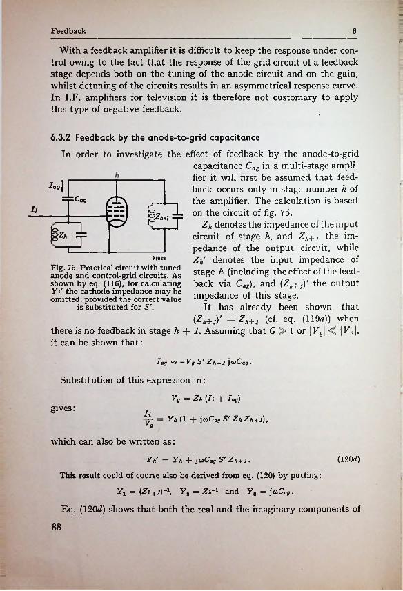
—
Feedback 6e
With a feedback amplifier it is difficult to keep the response under control owing to the fact that the response of the grid circuit of a feedback stage depends both on the tuning of the anode circuit and on the gain, whilst detuning of the circuits results in an asymmetrical response curve. In I.F. amplifiers for television it is therefore not customary to apply this type of negative feedback.
6.3.2 Feedback by the anode-to-grid capacitance
In order to investigate the effect of feedback by the anode-to-gridcapacitance Cag in a multi-stage amplifier it will first be assumed that feed-
Joyj back occurs only in stage number h of the amplifier. The calculation is based on the circuit of fig. 75.
Zk denotes the impedance of the input circuit of stage h, and Zh+1 the impedance of the output circuit, while Zk denotes the input impedance of stage h (including the effect of the feed-
—i-C0p §ii yo8*w -r
I* =rt
71029
Fig. 75. Practical circuit with tuned anode and control-grid circuits. As shown by eq. (116), for calculating back via Cflg), and (Zh+j)' the output y i' the cathode impedance may be omitted, provided the correct value
is substituted for S'.impedance of this stage.
It has already been shown that CZh+LY =zh+i (cf- eq. (119a)) when
there is no feedback in stage h 1. Assuming that G 1 or | Vs\ | Va\, it can be shown that:
lag ^ ~Vg S' Zh +1 jwC«y .
Substitution of this expression in:
Vg = Zh (Ii + lag)
^ = Yh (1 + jcaCag S' ZhZh + i),gives:
Vg
which can also be written as:
(120 d)Yh' — Yh + j caCag S' Zk +1.This result could of course also be derived from eq. (120) by putting:
Yx = (Zh+l)-\ Y2 = Zh’1 and Y3 = j <*Cag.
Eq. (120^) shows that both the real and the imaginaty components of
88
at
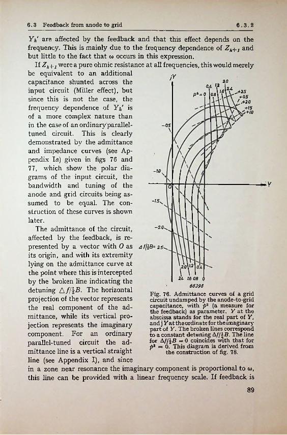
6.3 Feedback from anode to grid 6.3.2
Yh are affected by the feedback and that this effect depends on the frequency. This is mainly due to the frequency dependence of Zh+1 and but little to the fact that co occurs in this expression.
If Zh+1 were a pure ohmic resistance at all frequencies, this would merely be equivalent to an additional capacitance shunted across the input circuit (Miller effect), but since this is not the case, the frequency dependence of Y/,' is of a more complex nature than in the case of an ordinary'parallel- tuned circuit. This is clearly demonstrated by the admittance and impedance curves (see Appendix I a) given in figs 76 and 77, which show the polar diagrams of the input circuit, the bandwidth and tuning of the anode and grid circuits being assumed to be equal. The construction of these curves is shown later.
The admittance of the circuit, affected by the feedback, is represented by a vector with 0 as a f/iB= 2.5^, its origin, and with its extremity lying on the admittance curve at the point where this is intercepted by the broken line indicating the detuning A fl*B. The horizontal projection of the vector represents the real component of the admittance, while its vertical projection represents the imaginary component. For an ordinary parallel-tuned circuit the admittance line is a vertical straight line (see Appendix I), and since in a zone near resonance the imaginary component is proportional to co, this line can be provided with a linear frequency scale. If feedback is
jY2.0
0.4 \2 ,2408W\v>25, \ \>r +0.5pa= 0! .+2.0
+15
/ k/A/-05
\ K
\\
/
-1.0\-Yo\ \
\\\\N
\\
l\-2.0^ \'v
XX
\
12.0\-2
2.4 1.6 0.8 66398
Fig. 76. Admittance curves of a grid circuit undamped by the anode-to-grid capacitance, with p2 (a measure for the feedback) as parameter. Y at the abscissa stands for the real part of Y, and j Y at the ordinate for the imaginary part of Y. The broken lines correspond to a constant detuning Af/hB. The line for Af/$B = 0 coincides with that for p2 = 0.“ This diagram is derived from
the construction of fig. 78.
89
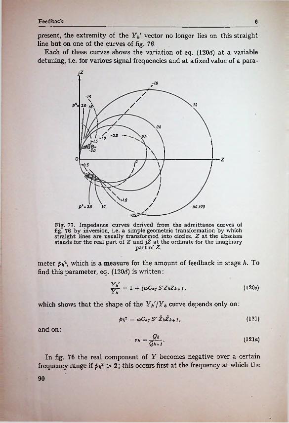
Feedback 6
present, the extremity of the IV vector no longer lies on this straight line but on one of the curves of fig. 76.
Each of these curves shows the variation of eq. (120d) at a variable detuning, i.e. for various signal frequencies and at a fixed value of a para-
jz
7W/-1.5 /\
Pa= 2D ,X / 1.2\ /
\0.8/
/ --------/ .0.41-1-5
flsB= \-2.0 \\0 •z1° \+0.5
\ /.\
//\
S'+/.0 //p2= 2.0 1.6 66399/-Q£7
Fig. 77. Impedance curves derived from the admittance curves of fig. 76 by inversion, i.e. a simple geometric transformation by which straight lines are usually transformed into circles. Z at the abscissa stands for the real part of Z and jZ at the ordinate for the imaginary
part of Z.
meter pj?, which is a measure for the amount of feedback in stage h. To find this parameter, eq. (12(W) is written:
Yj = 1 ay S'ZhZh +1, (120e)
which shows that the shape of the Yh/Yh curve depends only on:
ph~ = OiCug S' ZhZh + 1, (121)
and on:Qk (121a)Yh = TP—.Qh+1
In fig. 76 the real component of Y becomes negative over a certain frequency range if ph2 > 2; this occurs first at the frequency at which the
90
6.3 Feedback from anode to grid 6.3.1
circuits are detuned towards lower frequencies, so that an attenuation of i/2 is obtained. At this frequency the circuit may become unstable if the critical value pi? = 2 is exceeded.
The same result is obtained when theNyquist criterion for the stability of feedback circuits is applied. According to this criterion the circuit may oscillate when in the feedback loop (grid circuit - valve - anode circuit - anode-to-grid capacitance) the gain is equal to unity at a phase shift of 0° or n- 360°, n being a whole number. This will be the case when:
5' Zh + ioCagZh — 1at a frecuency such that the sum of the phase angles of the two circuit impedances is 90°, so that the phase shift due to jwCai7 is compensated. When the two circuits are identical this condition is satisfied at a detuning of 45°, so that:
Z
The oscillatory condition is therefore:
toCag S' Zh Zh +i = 2.
The Y and Z curves of figs 76 and 77 apply to circuits which are affected by the Cag of a valve loaded by a parallel-tuned circuit, the resonance frequency of which is the same as that of the grid circuit but which is not affected by feedback. In that case (Z/t+i)' = Zjl+1 = Z*. In practice, however, several stages in cascade are used, intercoupled by circuits which are sometimes detuned and all of which are undamped by the Cag of the following valve. For these conditions, eq. (120e) may be written:
Y// 1 (120/)/ »(Yh+i) Y/t + i
Yh
in whichjZr2 (122)= prZhZh+i’
pr2 = ttCagr S' Zr\
where Zr is the impedance of the "reference circuit” of the staggered tuning system (see Section 2.2).
By expressing (Yh+jY/Yh+i again in terms of and (Yj,+2y/Y/t+2, and so on, the expression for(Y/t-f jY/Yj,+: assumes the form of a continued fraction. When these continued fractions are worked out, Zr, the quantities pi? and the circuit impedances Z/* will appear in the final result. Once the tuning frequencies, the amount of damping and the bandwidths
where(123)
:1!
i91
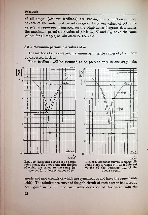
Feedback 6
of all stages (without feedback) are known, the admittance curve of each of the undamped circuits is given for given values of pn2. Conversely, a requirement imposed on the admittance diagram determines the maximum permissible value of pr2 if Zr, S' and Cag have the same values for all stages, as will often be the case.
6.3.3 Maximum permissible values of p2
The methods for calculating maximum permissible values of p2 will now be discussed in detail.
First, feedback will be assumed to be present only in one stage, the
¥ //15 ~P%=0\ fo V\
t\ 0,5
fI2
ihij5
A fa =0-770 u
66400
Fig. 78a. Response curves of an amplifying stage, the anode and grid circuits of which are tuned to the same fre
quency, for different values of p2.
AAJOi
Fig. 786. Response curves of an amplifying stage of which p2 = 1, for different values of the detuning A fa of the
anode circuit.
anode and grid circuits of which are synchronous and have the same bandwidth. The admittance curve of the grid circuit of such a stage has already been given in fig. 76. The permissible deviation of this curve from the
92
6.3 Feedback from anode to grid 6.3.3
straight line (at p2 = 0) depends on various conditions, but it is clear that p2 must in any case remain sufficiently far below the limit value of 2.
In the case of p2 > 2, the circuit will oscillate at the frequency at which the imaginary part of Y/,' is zero. This frequency is lower than the resonant frequency of the anode and grid circuits, as can be seen from fig. 76.
At p2 = 2 the circuit is just bordering on instability, and it is clear that it is necessary to observe a certain margin of safety to avoid spontaneous oscillation and ensure a good response curve.
Fig. 78 shows the response curves for several values of p2. It appears from this figure that at p2 = 0.5 the irregularities in the frequency response curve are not very pronounced and a safety factor of about 4 will therefore suffice in many cases. When, however, the gain of the stage is varied by controlling the mutual conductance of the valve, the detuning and variation of bandwidth may become excessive at p2 = 0.5, so that a higher safety factor will be required. The detuning A fag by the anode-to- grid capacitance may be roughly determined by taking the Miller capacitance as:
Cjj = Cag • G = CagSZh +1,
wCJIhence
= />=.Yh
At a detuning of l-B the value of Y/t is equal to coAC (cf. Appendix 1, fig. 107), and since
ACj AAAC., * ’ A/o ’
the detuning caused by the Miller capacitance is:
A/ag = }B-p'-.
The limit of stability can also be calculated from fig. 79#, i.e. the vector diagram from which fig. 76 was derived. The construction, of fig. 79# follows from eq. (120rf). A vector of length coCagS'Z/t+j, which is perpendicular to the Zn+j vector, must be added to the Y/, vector. Now Yh+j is identical to Y/t — the locus of which is a straight line — so that Zn+j (derived from Yh+j by inversion) is represented by a circle. The construction of Zu+j is based on the fact that its phase angle is numerically equal but of opposite sign to the phase angle of Y/,+j. The locus of the vector jtoCasS'Zjl+1 is also a circle, but with the point of origin shifted over 90°.
93
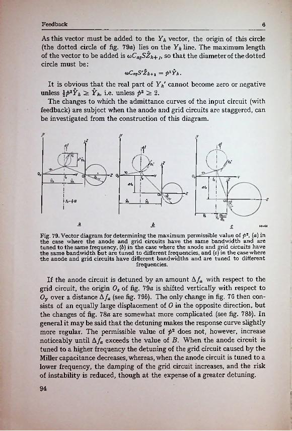
Feedback 6
As this vector must be added to the Y/, vector, the origin of this circle (the dotted circle of fig. 79a) lies on the Yjt line. The maximum length of the vector to be added is <nCanSZjl+lt so that the diameter of the dotted circle must be:
CiCagS'Zh + i = pzYh-
It is obvious that the real part of Y;/ cannot become zero or negative unless \p~Yh ^ Y/„ i.e. unless p2 ^ 2.
The changes to which the admittance curves of the input circuit (with feedback) are subject when the anode and grid circuits are staggered, can be investigated from the construction of this diagram.
£tI r \i \ /r A j* \
vj0/ * °> ^0
* laa1a
!Yh Yh
IYh
AA tMH
Fig. 79. Vector diagram for determining the maximum permissible value of p-, (a) in the case where the anode and grid circuits have the same bandwidth and are tuned to the same frequency, (b) in the case where the anode and grid circuits have the same bandwidth but are tuned to different frequencies, and (c) in the case where the anode and grid circuits have different bandwidths and are tuned to different
frequencies.
If the anode circuit is detuned by an amount Afa with respect to the grid circuit, the origin 0Z of fig. 79a is shifted vertically with respect to 0y over a distance A fa (see fig. 796). The only change in fig. 76 then consists of an equally large displacement of 0 in the opposite direction, but the changes of fig. 78a are somewhat more complicated (see fig. 786). In general it may be said that the detuning makes the response curve slightly more regular. The permissible value of p2 does not, however, increase noticeably until Afa exceeds the value of B. When the anode circuit is tuned to a higher frequency the detuning of the grid circuit caused by the Miller capacitance decreases, whereas, when the anode circuit is tuned to a lower frequency, the damping of the grid circuit increases, and the risk of instability is reduced, though at the expense of a greater detuning.
94f
6.3 Feedback from anode to grid 6.3.1
A second change to which fig. 79a is subject in the case of staggered tuning is manifest in the change of bandwidth of the anode circuit compared with that of the grid circuit. This results in a change of the Afa scale of Zh+1 (see fig. 79c). The curves of fig. 76 are now expanded or contracted in the vertical direction, but it is clear that in this case, too, instability is likely to occur when pi? ^ 2.
It is therefore advisable also in the case of staggered tuning to choose a value of pi? which has a safety factor of, say, 4 with respect to the limit value of 2.
It is true that there are cases which are stable although p2 > 2, but it is then necessary to avoid a particular value of the anode circuit detuning Afa. These frequencies then form the unstable region of the grid and anode circuits. This region increases with the value of p2 and disappears at p2 < 2.
If in a circuit p2 > 2 it may occur that the unstable region is encountered when the set is being trimmed. During the trimming of a particular circuit the other circuits should then be damped to avoid this troublesome phenomenon.
6.3.4 Staggered tuning
In practice the staggered circuits are given different bandwidths by varying the values of Zh, the circuit capacitances remaining practically unchanged, i.e.:
ZrZh = sin ah
hence:uCagS'Zr* Pr2p/r = sin ah sin a/4+1 sin ah sin oca +1 ’
in which a/* is the staggering angle of circuit h. It follows from this expression that the entire amplifier will not have the desired stability unless n conditions of the form:
(124)pr2 p/r sin a* sin cth + i
are satisfied in which p}? « 0.5. In these formulae the staggering angles of two successive stages will always be found, and to avoid the necessity of an extremely low value of pr2, it is advisable to arrange the amplifier such that slightly and heavily detuned circuits follow each other alternately. Should this be impossible, then provision should at least be made for the successive stages to be alternately detuned, as far as possible, to either side of Zr> the permissible value of pi? being thereby slightly
95
Feedback 6
increased. The fact is that if the limit of stability must necessarily be approached, more is to be feared from the reduction of damping than from the detuning caused by the feedback. In that case the grid circuit should be tuned to a higher frequency rather than the anode circuit (cf. fig. 78b).
It will now be investigated how the vector diagram of fig. 79 has to be constructed if the circuit Ji+1 is also the input circuit of an amplifier stage and is undamped via the anode-to-grid capacitance Cag. The locus of the vector {Zh+iY is then no longer a circle, but one of the curves of fig. 77, corresponding to the value of (p/l+1)2. Since it is desirable that not only the response curve of circuit h but also that of circuit li-\-l has a regular form, the value of {ph+j)2 must be chosen fairly low. According to fig. 77, this will result in the locus of the (Zj^j)' vector differing but little from that of a circuit without feedback and having a maximum impedance of
Zh + i1 -Upn+i)2'
This expression will become clear when the minimum value of (Y/,+ 2)' is calculated from eq. (120e) (see also fig. 76). In the construction the (Z/t+2)' diagram is approached by the circular diagram of the vector of the above- mentioned expression.
If it is desired to give circuit h a feedback parameter pi?, the stage in which this circuit li is connected to the grid of the valve must be designed for a smaller value of p2, viz.:
p2 = OiCagS'Z/iZh +1 •
Since the actual amount of feedback is determined by:
Zh + lph2 = (oCaffS'Z/^Zh + l)' = coCagS'Zh •
the conditionP2 = pn2 {1 — £(/>/*+j)2 }
i
must be satisfied. Since \(ph+i)2 is usually kept well below unity, p2 need not differ appreciably from the chosen value of pi?. An exact calculation of the required value of pi? according to the rather complicated method indicated at the end of Section 6.3.2 is therefore not necessary, and in practice it will suffice to determine pi? as if there were no feedback in the other stages and to use the value thus found in all further calculations. It should, however, be taken into account that the product toCagS,ZilZjl+1 is lower than the value of pi? that determines the amount of feedback in stage h, by a factor 1 — \(ph+i,)2-
* 96
6.3 Feedback from anode to grid 6.3.5
It should be realized that this method becomes less accurate when heavy feedback is present. As a result of this feedback the difference between (Za+J)' and Zjt+1 will then be considerable, so that the response curve of this circuit will deviate greatly from the desired shape. As a rule measures will then be taken to compensate these deviations, at least partially, by detuning and additionally damping circuit h-\-l, thus rendering (.Zj,+)i near its resonance again almost equal to the value prescribed by the staggering scheme. In this case also pj? can therefore be calculated as if feedback were present in stage li only. It will then, necessary be however, to fill in the corrected value for (Z/j+j), which is almost equal to the value required by the staggering scheme.
6.3.5 Maximum permissible gain
It will now be assumed that the maximum permissible value of p2 has been determined in accordance with the preceding formulae. The maximum permissible gain Gmax of each stage will then obviously be determined by the characteristics of the valve. For a staggered amplifier it follows from eq. (123) that:
<s'^2 = ■ =§; max (125)2rzfiCag
This expression can be further simplified by introducing the concept of stability reference frequency/8:
max (126)2lzCag ’
which finally gives:
ft- (127)Gr max = pr max
This expression shows that f& is the frequency at which Gmax would be equal to pmax, assuming the above formulae to be valid even at the high frequencies concerned. This assumption, however, is by no means permissible, since at these frequencies the "dynamic value” of Cag, which determines the feedback, is no longer equal to the "static value”, valid at low frequencies. /s is, therefore, only an extrapolated value by means of which the permissible gain, in the range for which eq. (125) is valid, can be determined.
In Section 2.2.2 it was shown that, at the mid frequency, Gh, i.e. the gain of stage li, is equal to Gr, the gain of a stage with the reference circuit
977
Feedback 6
connected to the anode of the valve. Substitution of the value of pr from eq. (124) therefore gives:
Gh <; ph V sin a/, sin a/, + i • j ftl.
As already shown, a reasonable value for pi? is, say, 0.5. In practice ph Vsin ah sin a;,+ J can be about 0.5. This roughly amounts to:
(128a)
ft-Ghmax ^ 0.5 (1285)
or (at the mid frequency!), for an amplifier with n stages:
(G tot max 0.5 (128c)
ExampleWhat will be the maximum permissible gain per stage of an I.F. amplifier for
35 Mc/s with a flat staggered quintuple if valves EF 80 are used and the circuit is also to remain stable (with a safety factor 4) during trimming?
According to Table 3 (p. XX) the smallest value of sina/, is 0.31. Combining this value with sin a/t +1 = 1 gives:
V sin a/t sin a/4 + 2 = 0.56.Table 1 (p. 168) shows that, for the EF 80, /« = 17 • 10‘ Mc/s, so that:
V-s17 • 104Ghmnx —■ 0.7 • O.o6 = 27.
If the sequence of the circuits were chosen less favourable so that the two values sina/t = 0.31 and sin ah + i =0.31 are combined, the maximum permissible gain would be considerably less, viz.:
V .517 • 104Ghmax — 0./ • 0.31 = 15.
A slightly higher value of G/,mnx could be afforded in this case, since the limit of instability cannot be approached unless both circuits are considerably mistuned.
6.3.6 Coupling by means of band-pass filters (I.F. transformers)
It would as a rule result in a reduction of the maximum permissible gain if the same stringent requirements were imposed on circuits coupled by band-pass filters as on those coupled by single-tuned circuits.
This may be illustrated by the following example. The transimpedance of a bandpass filter with q = 0 is also zero, and so is the gain of an amplifier containing such stages. The input and output impedances of the band-pass filters, however, differ from zero, so that the circuit may become unstable even at zero gain.
If the circuit is required to remain stable during trimming (without special precautions being taken) the maximum permissible gain per stage is smaller by a factor of at least 2 than in single tuned circuits.
98
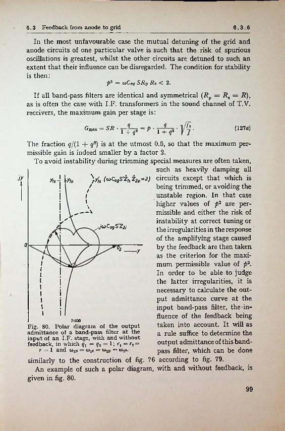
6.3 Feedback from anode to grid 6.3.6
In the most unfavourable case the mutual detuning of the grid and anode circuits of one particular valve is such that the risk of spurious oscillations is greatest, whilst the other circuits are detuned to such an extent that their influence can be disregarded. The condition for stability is then:
p~ = OiCag SRp Rs < 2.
If all band-pass filters are identical and symmetrical (Rv = Ra = R), as is often the case with I.F. transformers in the sound channel of T.V. receivers, the maximum gain per stage is:
Wfi<1 (127a)Gmax = SR • l + g2
The fraction q/( 1 -f q2) is at the utmost 0.5, so that the maximum permissible gain is indeed smaller by a factor 2.
To avoid instability during trimming special measures are often taken,such as heavily damping all
\yj0 (<*CagS'ZhZ2p=2) circuits except that which is being trimmed, or avoiding the unstable region. In that case higher values of p2 are permissible and either the risk of instability at correct tuning or the irregularities in the response of the amplifying stage caused by the feedback are then taken as the criterion for the maximum permissible value of p2. In order to be able to judge the latter irregularities, it is necessary to calculate the output admittance curve at the input band-pass filter, the-influence of the feedback being taken into account. It will as a rule suffice to determine the output admittance of this bandpass filter, which can be done
76 according to fig. 79.An example of such a polar diagram, with and without feedback, is
given in fig. 80.
Ijy yi5-\ y/io/
/i\
✓JwCagS'Z#/
(/0 %
71030Fig. 80. Polar diagram of the output admittance of a band-pass filter at the input of an I.F. stage, with and without feedback, in which qx = q« = 1; i\=r2 =
y — 1 and cOj/j = co^s = Wop = Wos.
similarly to the construction of fig.
99
Feedback 6
This procedure has the drawback of being rather cumbersome. A less accurate method that saves much time consists in roughly determining the magnitude of the maximum relative change to which the Yh vector is subject when the feedback admittance is taken into account. In the case of a single circuit, the relation
\Yh'—Yh\ : \Y/,\ = 0.5
(at p2 = 0.5) was taken to be permissible.It may now be assumed that the permissible ratio is of the same order
when the coupling consists of a band-pass filter, Y/t then representing the output admittance of this filter at the grid side.
In order to apply this procedure to stagger-damped band-pass filters of which Qp = oo, the admittances Yi and Y0 of such a band-pass filter must first be expressed in terms of the quantities x8 and qs, which are related to the secondary only, namely:
Ys — SC„a1'Yi = (129)and
= Ys(l + +Y0 (130)in which
Ys = I?s, *s = ps0s and qs = kQs.
From these formulae it follows that the output admittance is the minimum when Xs = db ?s. For the frequencies at which this is the case, at a variation of xs, the phase of Y0 changes much more quickly than that of Yi. Y0' passes through its minimum value in close proximity to \xs\ = qs, which — as far as stability is concerned — is the most critical area.
From the staggering scheme it can easily be derived that, for the reference circuit in this region, xr & 1. Hence, from eqs (129) and (130):
17 1 17 I 7 2 VT -f- sin2 cth +1\Zh\ • \Zh + l\ ^ Yr2 • ----------- :---------- .11 1 sin a* • sm a/(+j
(131)
It is clear that the maximum permissible gain largely depends on the staggering scheme in this case also. It is possible to choose this scheme so that eq. (131) assumes its minimum value for the critical stages. A rough calculation in which the mean value of sin a is taken to be approximately 0.7 gives:
fr (128^)Gmax ^ 0.8
which appears to be slightly higher than the value of Gmax found for the case where single circuits are used. It should, be realized however, that in the deduction of the formula for single circuits the exact point of the
100
i
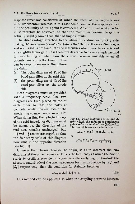
6.3 Feedback from anode to grid 6.3.6
response curve was considered at which the effect of the feedback was most detrimental, whereas in this case some point of the response curve “in the proximity of” this point is considered. An additional safety factor must therefore be observed, so that the maximum permissible gain is actually slightly lower than that of single circuits.
The disadvantage attached to the above procedure for quickly estimating the maximum permissible gain is that the results are rather vague and no insight is obtained into the difficulties which may be experienced at a slightly larger gain. It is therefore desirable to have a simple method for ascertaining at what gain the circuit becomes unstable when all circuits are correctly tuned. This can be done by means of the following data:(a) The polar diagram of Z0 of the
band-pass filter at the grid side;(b) the polar diagram of Z\ of the
band-pass filter at the anode side.
Both diagrams must be provided with a frequency scale. The two diagrams are then placed on top of each other so that the poles 0 coincide, whilst the real axis of the anode impedance leads over 90°.When doing this, the reflected image of the grid impedance diagram must be taken, i.e. the direction of the real axis remains unchanged, but -f-j and—j are interchanged, so that the frequency scale of this diagram now runs in the opposite direction (see fig. 81).
A line is then drawn through the origin, so as to intersect the two diagrams at the same frequency. This is the frequency at which the circuit starts to oscillate provided the gain is sufficiently high. Denoting the absolute magnitude of the two impedances for this frequency by \Za'\ and \Zg \ respectively, then tlie condition for stability becomes:
wCflj 5 \Za \ IZg \ < 1.
This method can be applied also when the coupling network between
____ Zu
----- 0-7 q2-l571031
Fig. 81. Polar diagrams of Z0 and Zi from which the maximum permissible gain can be ascertained. r=Qs\Qj> = 0.5. The circuit becomes unstable when:
<x>Cag S' 0.3 Zjj 0.56 Zop — 1,
1(iiCag S'Z-ys Z2p- — 0.3 • 0.56 '
(132)
101
I
Feedback 6
the stages is of a more complex nature and consists, for example, of a circuit with wave traps for suppressing undesired signals.
The above method can easily be derived from the Nyquist criterion, in which case the polar diagrams of the complex gain y = Ea/Eg and of the complex feedback factor p are determined. For the circuit to become unstable it is necessary that the sum of the phase angles of these two diagrams bezero, whilst the product |y|*|P| must moreover be equal to or exceed unty at the frequency at which this condition is satisfied.
These conditions can be expressed by:yp = OiCay S \Za'\ \Zg\ 1.
6.3.7 Deviations at higher frequencies
The above comments apply to I.F. amplifiers operating at frequencies below 30 Mc/s. At higher frequencies however, it is necessary to take into account the fact that the dynamic feedback capacitance Cag may differ considerably from the static value Cag (see Other Forms of Feedback, Section 6.6).
In the first instance C„g' decreases with the frequency and finally assumes a negative value. In this range:
c. = c^-(g},where // is the frequency at which Cag is zero.
The calculation of the maximum permissible gain could be corrected by introducing a quantity fs which depends on the signal frequency. It is, however, simpler to determine fs from the static value of Cag and to correct the equation for the maximum permissible gain as follows:
(133)
K'{-W (128(f)Gmnx — pmtix
The values of fs' are not valve constants, but also depend to a certain extent on the wiring, the valve holders, etc. For an EF 80 tube// « 70 Mc/s in normal circuits.
At frequencies exceeding // the maximum permissible gain G rapidly decreases. Since the sign of the feedback admittance is now reversed, damping occurs at those detunings at which originally regeneration occurred, and vice versa.
When the signal frequency is further increased the transit time t usually also starts to play a part in the stability condition. Although the magnitude of S' remains practically unchanged, the phase shift may become quite considerable at frequencies from 100 Mc/s to 200 Mc/s. It is
max
102
6.4 Feedback by the cathode-to-grid admittance
due to this phase shift that the distortion of the response curve caused by the feedback is of a more symmetrical nature. When /t = £ this distortion is purely symmetrical.
6.4 FEEDBACK BY THE CATHODE-TO-GRID ADMITTANCEThe investigation of the effect of feedback by the cathode-to-grid
admittance is again based on equations (115) and (117). The admittances Y3 and Y5 (see fig. 72) are assumed to be zero, so that p and Y7 also become zero. This gives:
Yo = Yx = Yo,_ Y,
y0 + y4 + S/c ~i (134)Fsand i +StZt (i + ^)'
The input admittance is thus:Yx = y2 +
Eq. (135) is now applied to a few practical circuits, where the input admittance of the valve is governed by:
the capacitance Cgl of the control grid to earth (Y2), the capacitance Cglk of the control grid to the cathode (Y4), the capacitance Cglg2 of the control grid to the screen grid (Y2), the conductance g^ of the control grid to earth (Y2), the conductance of the control grid to the cathode (Y4), i.e. mainly
the transit time damping gr, andthe impedance in the cathode lead, consisting of a real component and
an imaginary component connected in parallel, i.e.:
i- = Y0 = g0 4- A •
Y0y.t (135)yo 4- y4 + Si,-
^0
Eq. (135) can be developed to:Yx = ggi 4- jo>(Cyi 4- Cgm) 4- go4-gx4- Sk 4- j60
a>Qi*go 4- frog?4-j go 4- gx 4“ *Sk 4- 4- j50By eliminating the imaginary components from the denominator the
third term becomes:(gxgo — <oCglA-50) { (go 4- £t4- Sic) — j(coCglt 4- &o) }
(go 4“ g"z 4” Sic)“ 4“ (coQjt 4- &o)2
and the fourth term becomes:(oiCg^gg 4~ & pgr) { (go 4~ gT 4~ Sk) ---j(coC;/ifc 4- bp) }
(go 4- gx 4- 5a)2 4- <*Cgxic 4- b{j)2j
103
Feedback 6
The input damping is thus 2)
gi' = gg i +
which may also be written as:
(&t^c <oCyift66) (g6 + gr 4- (oC^Ago + frogr)(§6 + + Si)2 + (toCyji + &6)2
vCgikg* — V^-gi' — goi + <*>Qi* * 2 “h(go + g-z + Si)2 -\- (coCj/ji + bG)
g62 +A2 + gG (Si +jrT)___ (go + gr + Si)2 + (wCj/ii + 6e)2+ St* (136)
The magnitude of the imaginar}^ component of Y/ is now:(Yi') imaginary = 4~
(ojCgjj 4~ b0) ((oCgljfc0 — gcgr) 4~ (<oCyiig0 -f- ^c&t) (go ~f~ gr + Sj)(go + g'r + Si)2 + (coQrji + 50)2
which corresponds to an input capacitance of:
go(go + Si) 4- b61 &6 -f- oiCfflk + (gv + Si) • ^^7 -1Ci' — Cgl 4- CgxJ72 4" Cgxk • .(137)
(go + gr + Si)2 4- (wC^i 4- 6C)2
By means of eqs (136) and (137) it will now be shown how the various cathode impedances influence the input circuit. Once the input conductance gi has been calculated from eq. (136) for a particular case, the simplified expression thus obtained will be used to calculate the input conductance when other effects are considered. The following effects are of importance:(1) the damping caused by the self-inductance of the cathode lead,(2) the compensation of this damping when using an additional cathode
capacitor,(3) the variation of the input capacitance by incorporating a small
resistance in the cathode lead,(4) the variation of gi and C{ if a resistor shunted by a fairly small
capacitor is included in the cathode lead.
6.4.1 Self-inductance in the cathode leadIt is assumed that a very small self-inductance L* is present in the
cathode lead, so that:St
toLkSk <1 or — 1,°owhile
£ < P<1b 6 bo*) It is only in this section that, in analogy witfl the convention of p. 85, the
input damping is denoted by gi'.
104
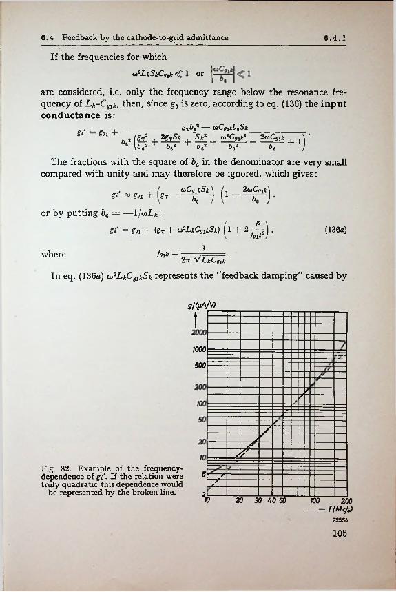
6.4 Feedback by the cathode-to-grid admittance 6.4.1I
If the frequencies for which
w 2L kSkCgik < 1 or
are considered, i.e. only the frequency range below the resonance frequency of Lk~Cslk, then, since g6 is zero, according to eq. (136) the input conductance is:
gi' = g'Ji + gx^o3 — <jiC9lkb0Sk
v(f? + <*zCgik2 , 2taCgl* \ 'V + K + J
The fractions with the square of b6 in the denominator are very small compared with unity and may therefore be ignored, which gives:
OiC/jikSk
Sk2+ +v- b o2
gi' * gn + (gT-
or by putting bG = —1/coZ,*:
gi' = g'Jl + (g~ +
■)(*
■
2<oCf/ji
be be
(H~LkCfji/;Slc) ^ 1 -f* 2 » (136a)
1fm* =where 27- VLkCgik
In eq. (136a) co^C^S* represents the "feedback damping” caused by
g/fyA/V)
t1000
500
77
7_____“Z
/Fig. 82. Example of the frequency- dependence of giIf the relation were truly quadratic this dependence would
be represented by the broken line.
5 7~r2L
10 20 30 40 50 100 200
72556
105
ii
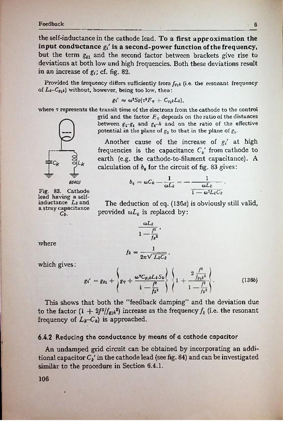
Feedback 6’
the self-inductance in the cathode lead. To a first approximation the input conductance gi is a second-power function of the frequency, but the term ggl and the second factor between brackets give rise to deviations at both low and high frequencies. Both these deviations result in an increase of g,-; cf. fig. 82.
Provided the frequency differs sufficiently from ftJlk (i.e. the resonant frequency of Li~Cgik) without, however, being too low, then:
gi' sv oj2Sa (t2Ft + CgiicLi),where t represents the transit time of the electrons from the cathode to the control
grid and the factor i?T depends on the ratio of the distances between gy^i an<i S\~^ and on the ratio of the effective potential in the plane of g2 to that in the plane of gv
Another cause of the increase of gi at high frequencies is the capacitance Ck' from cathode to earth (e.g. the cathode-to-filament capacitance). A calculation of b6 for the circuit of fig. 83 gives:
l l66403
Fig. S3. Cathode lead having a selfinductance L*and a stray capacitance
OlLl;1 — oi2LkCk
The deduction of eq. (136a) is obviously still valid, provided coLk is replaced by:
coLk
Ck.
1-4’A2
where1fk =
2t:V LkCkwhich gives:
(OiiCgikLkSk (1366)Si' — S'Ji + 'i o T *r
i fk2
This shows that both the "feedback damping” and the deviation due to the factor (1 + 2/2//gl*2) increase as the frequency (i.e. the resonant frequency of Lk-Ck) is approached.
6.4.2 Reducing the conductance by means of a cathode capacitor
An undamped grid circuit can be obtained by incorporating an additional capacitor CA/ in the cathode lead (see fig. 84) and can be investigated similar to the procedure in Section 6.4.1.
I
106
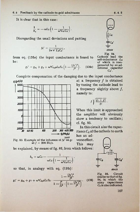
6.4 Feedback by the cathode-to-grid admittance 6.4.2
It is clear that in this case:
= — i»Lk ^ ll 1*"o g>2L*C*7 '
Disregarding the small deviations and putting
l/*' = 2 WLtCic’' 66404
Fig. 84.Cathode lead the self-inductance Lk of which is compensated by an additional capacitor
C*'.
Complete compensation of the damping due to the input conductanceat a frequency / is obtained by tuning the cathode lead to a frequency slightly above /, namely to:
from eq. (136«) the input conductance is found tobe:
§i' — gm +ott <»2CgikLkSk 11 (136c)
9j(yA/V)5000
X
/
\l When this limit is approached the amplifier will obviously show a tendency to oscillate; cf. fig. 85.
In this circuit also the capac- 200 300 400500 itance Ck of the cathode to earth----- -- ftfMc/s)
72557
0
too30 4050
has an ad-Fig. So. Example of the influence of fk' ongi verse effect.
This maybe explained, by means of fig. 86, from which follows:
at / = 200 Mc/s.
r~ib6 = 6iCk :)l =T=^ tc*'oiLk 1
<*-LkCk' !
so that, in analogy with eq. (136c):
l _(/*T
66405
Fig. 86. Circuit similar to that of fig.
(138) 84, in which thestray capacitance Ck is also indicated.
r-gi' = goi + g* + Oi-CijikLkSk •
A2107
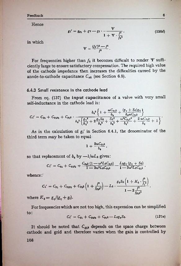
6Feedback
Hencexy
gi' = go 1 + g* — gt • (136rf)1 + T • A
/*2in which
xV (hT-~ r-
—r-
For frequencies higher than /* it becomes difficult to render Y sufficiently large to ensure satisfactory compensation. The required high value of the cathode impedance then increases the difficulties caused by the anode-to-cathode capacitance Cak (see Section 6.5).
I6.4.3 Small resistance in the cathode lead
From eq. (137) the input capacitance of a valve with very small self-inductance in the cathode lead is:
V {1 +■
i<*Cyik (g~ -f- Sk)gr }6c<oCgi/;&6Cl = Cgx + Cgxg2 + CgjJc • 2 oiCgxkSir , o>2Cgiir
I t. o "Ib 2 /fl! 2grSb-6 IV + V + 1 ;Vbe2
As in the calculation of gi in Section 6.4.1, the denominator of the third term may be taken to equal
2<x>Cgxk1 +*0 '
so that replacement of &6 by —1/wL^ gives:Cgik (1--- (i^LkCgik)__ LlcgT (gT -j- Sic)Cl = Cgx + Cgxg2 + 1 — 2ca2LkCgxk1 2c0-LkCgxk
whence:g^Sk ^1 + • jz j
+ Com + Ctit ^1 + J~j^j -Lk-Cif = Cgx r-1 ---2 J—Hfolk2where I<2= gT/(gT-f &)•
For frequencies which are not too high, this expression can be simplified
(137a)to:
Cl = Cgx + Cgxg2 + Cjjxk Lkg^Sk-I
It should be noted that Cglk depends on the space charge between cathode and grid and therefore varies when the gain is controlled by
108
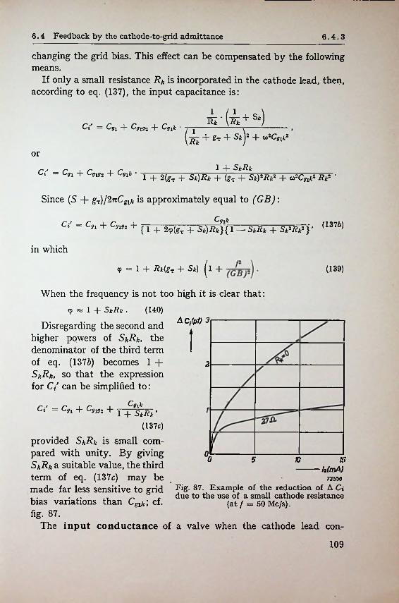
6.4 Feedback by the cathode-to-grid admittance 6.4.3
changing the grid bias. This effect can be compensated by the following means.
If only a small resistance Rk is incorporated in the cathode lead, then, according to eq. (137), the input capacitance is:
m' (-k +s*)Ci — Cgx + Cgmo + Cgxk '
[k + ^ + 4 + <*}ZCgxkZ
or1 + SkRkCl — Cgx + Cgxg2 + Cgxk ' 1 + 2(gx + Sk)Rk + (gx + S*)W + u-Cgik2 Rk2 ’
Since (S + gT)/2~Cglfc is approximately equal to (GB):
_________________ Qi*_________________{ 1 + 2y(gx + Sk)Rk}{ 1 — SkRk + Sk2Rk2}'Ci' = Cgx + Cgxg2 + (1376)
in which9 = 1 + Rk{gx + Sk) ^1 + (139)
When the frequency is not too high it is clear that:(140)
Disregarding the second and higher powers of SkRk, the denominator of the third term of eq. (1376) becomes 1 +SkRk, so that the expression for Ci can be simplified to:
Cg\k
1 + SkRk(137c)
9 *=» 1 + SkRk -A C,(pt) 3
12
Ci' — Cgx + Cgxgz +
provided SkRk is small compared with unity. By giving SkRk a suitable value, the third
00 5 10 IS
la(mA)72553term of eq. (137c) may be
made far less sensitive to grid Fig- 87- Example of the reduction of A Ci° due to the use of a small cathode resistance
(at / = 50 Mc/s).bias variations than Cgl*; cf. fig. 87.
The input conductance of a valve when the cathode lead con-
109
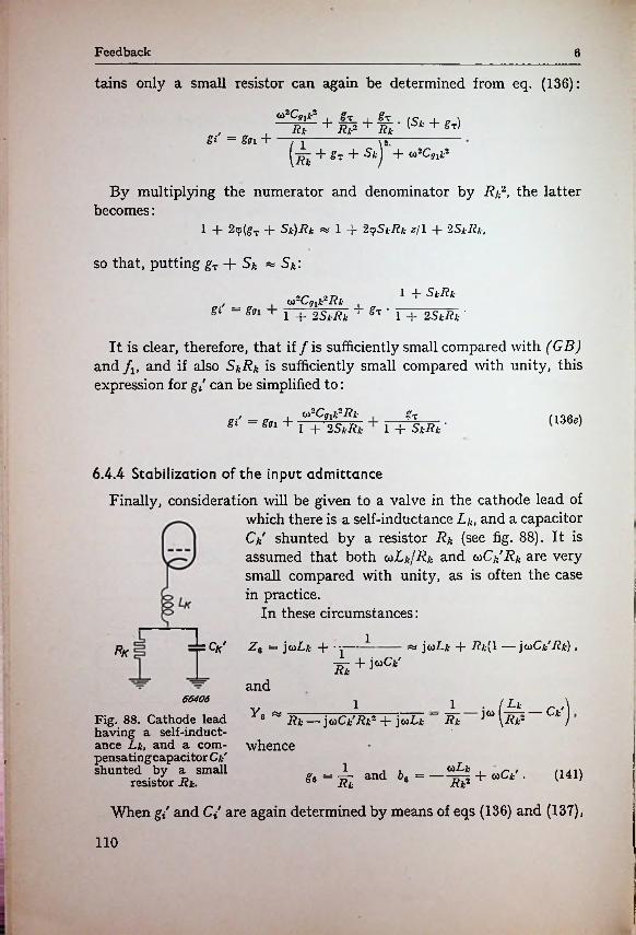
Feedback 6
tains only a small resistor can again be determined from eq. (136):
caaCg i<aRT + + Rk ' (S* + ?t)
Si' = #01 + (^ + ^ + s*)B}^ multiplying the numerator and denominator by Rk2, the latter
becomes:1 + 2<?(gT + Sk)Rk «! + 2? SkRk z/l + 2SkRk,
so that, putting gT + S* w S*:
1 -f- SkRk<ji-C(Jlk2Rk
Si' = &/1 + + S'- • 1 -f- 2SkRk1 + 2S*rt*
It is clear, therefore, that if / is sufficiently small compared with (GB) and flt and if also SkRk is sufficiently small compared with unity, this expression for g/ can be simplified to:
to“C{jjk“Rk 1 -f- 2SkRk
St (136e)Si' = Sn + 1 + SkRk ’
6.4.4 Stabilization of the input admittanceFinally, consideration will be given to a valve in the cathode lead of
which there is a self-inductance Lk, and a capacitor Ck shunted by a resistor Rk (see fig. 88). It is assumed that both uLk/Rk and uCk'Rk are very small compared with unity, as is often the case in practice.
In these circumstances:l
jwLjfc + /?*(! — ivCk'Rt).=<v Z0 = j<aLk + • v—% 1S + j"C*'
and66406
Fig. 88. Cathode lead having a self-inductance Lk, and a compensate g capacitor Ck' shunted by a small
resistor Rk.
When gi and C{ are again determined by means of eqs (136) and (137),
11Yg W Rk — ]o>Ck'Rk- + j toZ-A; Rk
whence<oLk1 15* + «cv . (141)*“35 and 60 =
1103.
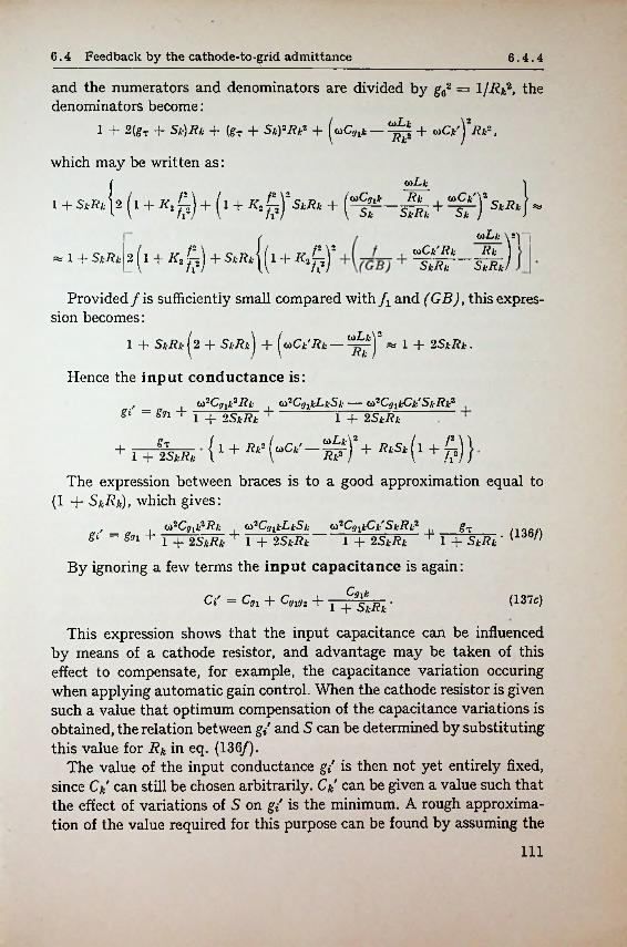
6.4 Feedback by the cathode-to-grid admittance 6.4.4
and the numerators and denominators are divided by g62 = l/Rk2, the denominators become:
1 + 2(gT + Sk)Rk + (gx + Sic)2jR/r + ----- -f coCfc'j Rt9,
which may be written as:GiLk j S*7?jt j ss
( <aCgik Rk oiCk'1 + SkRk SkRk ~f-Sk SkRk Sk
GiLk \2~j~j
(t1 + K-J?)^ 1 4" SkRk 12 ^ 1 -f- Kn j 4" SkRk oiCk'Rk RkSkRk SkRk/
Provided / is sufficiently small compared with f1 and (GB), this expression becomes:
|^2 + SA-/?A-j + ^ )oLkV1 + SkRk OiCk'Rk ** 1 + 2SkRk.Rk
Hence the input conductance is:<j)zCgik~Rk _j_ (j2CgikLkSk — <*-CgikCk'SkRk2
1 + 2 SkRkSi' Sol + 1 -f- 2SkRk
hm{1 + Rk- ( oiLkV)H--------— + RkSkoiCk'Rk21 + 2 SkRk
The expression between braces is to a good approximation equal to (1 -f SkRk), which gives:
co2Cgik2Rk <o*CnkLkSk <*2CgikCk'SkRk21 + 2 SkRk + 1 + 2 SkRk
By ignoring a few terms the input capacitance is again:1 + 2SkRk 1 + SkRk
. (136/)Si' = Sox +
Ci = Cgi + Cgig2 T (137c)1 + SkRk '
This expression shows that the input capacitance can be influenced by means of a cathode resistor, and advantage may be taken of this effect to compensate, for example, the capacitance variation occuring when applying automatic gain control. When the cathode resistor is given such a value that optimum compensation of the capacitance variations is obtained, the relation between g/ and S can be determined by substituting this value for Rk in eq. (136/).
The value of the input conductance g/ is then not yet entirely fixed, since Ck can still be chosen arbitrarily. Ck can be given a value such that the effect of variations of S on g/ is the minimum. A rough approximation of the value required for this purpose can be found by assuming the
111
Feedback 6
denominators in eq. (136/) to be constant and disregarding^. In that case gi appears to be independent of S when:
0i~C9lkUSk — €A*CgikCk'SkRk* = 0,Ck' = Lk (142)or:
WIn eq. (142) no longer appears, i.e. the compensation is to a first
approximation independent of the frequency.Alternatively, gt' could be rendered independent of S by tuning the
cathode lead by means of a series capacitor, but the compensation is then highly dependent on the frequency, so that the circuit is apt to become unstable. There is no such risk in the case discussed above, where the cathode capacitance is usually smaller than in the case of series tuning of the cathode lead.
In some cases the capacitance of the cathode pin (and the connected screens) to earth is large enough for the purpose in view. The capacitance Ck of the cathode itself to earth should not be taken into account here, since this is not shunted across C*'. This is demonstrated by the expression:
—toL;- (1 — v>-LkCk) (141a)«C*',K —
which shows that Ck has not the same effect on b6 as Ck-
6.4.5 Valves with double cathode connectionThe input conductance gi of some valves is given a low value by pro
viding two cathode connections which should be connected in parallel; by this artifice Lk is approximately halved.
When it is desired to undamp the grid circuit by tuning the cathode circuit it is not advisable to tune only one of the cathode leads and to use the other as a supply lead for the direct current, nor should the two leads be tuned to different frequencies. This might lead to instability due to the combination of the two cathode leads being in parallel resonance for one or several particular frequencies.
Furthermore, if AC,: compensation is not applied in the cathode circuit, advantage can be taken of the double cathode connection to reduce appreciably the active cathode lead impedance Lk by connecting the lower end of the grid circuit to the one cathode pin and the return lead of the anode circuit to the other pin J). To avoid instability the lower end
Rk-
i) Cf. M. J. O. Strutt and A. van der Ziel, A Variable Amplifier with Double Cathode Connection suitable for Metre Waves, Philips Techn. Review 5, p. 357, 1940 (No. 12).
112
6.5 Feedback by the anode-to-cathode capacitance
of the grid circuit must also in this case be screened from the anode Since the screening can of the anode circuit has to be connected to the lower end of this circuit, the anode return lead must be connected to earth, and the grid circuit thus remains floating. The capacitance to earth of this floating circuit and the inductance of both cathode leads give rise to another form of feedback, which may lead to instability at frequencies well above 100 Mc/s.
6.5 FEEDBACK BY THE ANODE-TO-CATHODE CAPACITANCEThe inclusion of an impedance Z6 in the cathode lead will result in
feedback to the cathode by the anode-to-cathode capacitance Cak, after which feedback to the control grid occurs via the grid-to-cathode capacitance Cglk. The anode-to-cathode capacitance Cak, therefore, has a similar effect in these circumstances to that of the anode-to-grid capacitance Cagi- As can be deduced from eqs (115) and (116):
V« + VtVi' = Y, + Y4 • Yc + Y7 + St — pSa ’
which, to a fair approximation, may be written:
y»yc + ^4 'Yt' = Y., 4- Y4 • Y0 + Y4 + Y7 + 5*Y0 + Y4 + Y- + SkP Sq+ y4 • Y6 + Y4 + Y, + Sk'
provided Y6 > Sk. By substituting
Yt + Yj ^ YxP =and
Y7 = (l —P)Y, « Y§,
and disregarding Y7 in the denominator,Y*Y*YgYi' = Yo + Y4 • Yfl + Y4 + SkYc + Y4 + Sk
Provided the gain is not too small, this expression may be approximatedas:
SaY,Y, ____________Yj Y0 + Y4 + St *
YeYi' = Yo + Y4 • Y6 + Y4 + 5a-
The “feedback term" (containing Y5) is now compared with the effect of the direct feedback from the anode to the control grid. This effect is expressed by (see eq. (120)):!
y3 «
1138
Feedback 6
or, from eq. (115), by setting p = 0 and Y7 = 0:Y. SqYcIT yfl + y4 + sk •
The feedback via the cathode circuit is therefore equivalent to a direct feedback produced by an admittance Y3' equal to:
Vo *(143)Y* =
Substituting jofor Y5, jcoCgl* for Y4 and jo>Cagi for Y3', eq. (143) becomes:
(144)CaiJi — Cak • j toCj/jfrZg.
This means that if a capacitor CV is included in the cathode lead, the capacitance Cagl' should not exceed the maximum permissible value.
The value of Cagl' can be calculated from eqs (126), (127) and (144), which give:
£max2 px max2
Smax (145)= <*>C0lkZJ •2n Cak
provided SkZ6< 1.
6.6 OTHER FORMS OF FEEDBACK
At frequencies exceeding 50 Mc/s the self-inductances and mutual inductances of various connecting leads of the valves will give rise to other forms of feedback.
Space does not permit full investigation of these effects, but it may be stated that their influence can be considered as a variation of Cagl'.
Due to the effects summarized below, Cagl contains other terms in addition to C(jgj and
Mutual inductance Magl between the anode and the control-grid leads gives rise to an additional term:
-j- <*2CaCgiMag1 •
Self-inductance Lg2 of the screen-grid lead gives rise to an additional term:
—ca2CagzCgigJLg2.
Mutual inductance Mglg2 between the control-grid and screen-grid leads gives rise to an additional term:
—(j)^Cg-yCagoMgig2 •
114
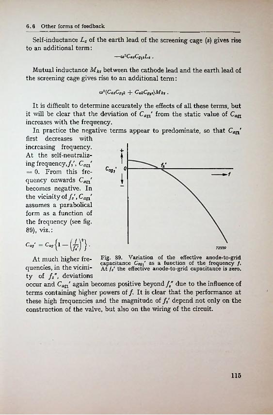
6.6 Other forms of feedback
Self-inductance Ls of the earth lead of the screening cage (s) gives rise to an additional term:
Mutual inductance between the cathode lead and the earth lead of the screening cage gives rise to an additional term:
Oi"'{CasC(/1k -f- CakCgi$}Mks •
It is difficult to determine accurately the effects of all these terms, but it will be clear that the deviation of Crtgl' from the static value of Cagl increases with the frequency.
In practice the negative terms appear to predominate, so that Cagl' first decreases with increasing frequency.At the self-neutralizing frequency,/s', Cagl'= 0. From this frequency onwards Cagi becomes negative. In the vicinity of fs\ Cflgl' assumes a parabolical form as a function of the frequency (see fig.89), viz.:
+t fs'
Cagi' 0
t
Cag'
At rmirh higher fre- Fig- 89. Variation of the effective anode-to-grid J* ... capacitance Cagi as a function of the frequency /.
quencies, m the vicim- At // the effective anode-to-grid capacitance isty of /s", deviationsoccur and Cagl' again becomes positive beyond f" due to the influence ofterms containing higher powers of/. It is clear that the performance atthese high frequencies and the magnitude of // depend not only on theconstruction of the valve, but also on the wiring of the circuit.
zero.
115
7. PRACTICAL CONSIDERATIONS FOLLOWING ONTHE THEORY
It will now be shown how the preceding calculations can be used when designing circuits for I.F. amplification in television receivers.
7.1 SENSITIVITY
The sensitivity required for a given amplifier will first be investigated. The minimum field strength for various frequencies at which a signal-to- noise ratio of 5 (= 14 db) can be attained is shown in fig. 70. From this cum it is possible to ascertain the smallest field strength Hmin that can be amplified to give full output. Once this choice has been made, the voltage across the input circuit of the amplifier is given by eq. (17):
Ha
The transformer ratio w need not be known if the required sensitivity at the aerial terminals only is to be calculated, since the voltage at these terminals is smaller than the voltage across the input circuit by a factor w. For a normal dipole aerial this voltage is given by:
50 Hm\nH miiAFmin — /2~
ExampleA television receiver for 50 Mc/s with a bandwidth of 5 Mc/s must be capable of
giving maximum output signal even when the signal-to-noise ratio at the output drops to 2 or even less. What should the sensitivity be at the aerial terminals?
From fig. 70 (broken lines, corresponding to conditions of minimum cosmic noise) the maximum output signal may be obtained at field strengths of approximately:
§ • 60 = 24 |xV/m .
Hence, according to the above formula:j. 50 //min OA tt Vmin = ---- ------- = 24 |ZV .
7.2 GAIN
In the case of a T.R.F. receiver the total gain Gtot, calculated from the aerial terminals to the anode circuit of the last I.F. tube, is given by the expression:
Gtot = w • .
116
7.2 Gain 7.2.1
In a superheterodyne receiver with a tuner, the gain GtUncr °* which is given, the total gain can be calculated from:
Gtot = Gtuner • Gn .
7.2.1 Gain of the input circuit
The gain of the input circuit of a receiver can be determined by means of eq. (136) in the frequency range below /0', or by means of eq. (106) for frequencies exceeding /</. The voltage gain G' thus found is the ratio of the voltage across the input circuit to the voltage at the aerial at zero load. (If the gain is understood to be the ratio w of the voltage across the input circuit to the voltage at the aerial terminals, twice this value must be taken, since w/2 = G'.)
In practice the admittance of the aerial circuit is not always negligibly small compared with the input admittance of the valve and the additional damping resistance. Since it is not possible to reduce gc below the extreme value gcmin, it is clear that:(а) Gq cannot exceed l/V47?ant gcmin, and(б) /0' cannot be lower than /V4i?ant gcmin.
Maximum gain is obtained when the circuit is not additionally damped, see fig. 90.
Apart from the transitional jogG* point at /o' being somewhat more rounded off, this diagram has the same form as fig. 3. As Gq (and thus also/,') approaches the above-mentioned boundary value, the effect of this curvature on the log G' = f(log /) curve steadily increases; by keeping a factor of aboVit 2 below the boundary value the rounding-off will be less than 10 %.
/V^Rant’Sc min
I------ — log /
72560Fig. 90. Diagram showing the variation of log G' as a function of log /. In contrast to fig. 3 the circuit conductance is constant,
viz. gcmin.
7.2.2 Gain of the I.F. amplifier
In the calculation of Gtot the term Gn is always the main factor. To evaluate Gn it must first be investigated whether the valves operate above or below fQ (cf. eq. (12a)). As a rule the latter will be the case, so that G can be calculated from eq. (13a):
B • G = F,FX(GB).
117
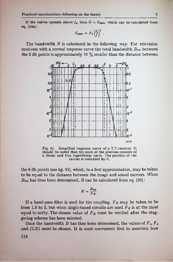
Practical considerations following on the theory 7
If the valves operate above /„, then G = Gmax, which can be calculated from eq. (10a):
r _ p- (fi\2 'J'max — yj-J ■
The bandwidth B is calculated in the following way. For television receivers with a normal response curve the total bandwidth jBtot between the 3 db points is approximately 10 % smaller than the distance between
10 (3($*~2 c,i 0.5 0 0.5 1? 21"N
Q5 0.5
S=50.2
1(T1 JO''
5 5
2 2
10~2nr25 5
2 2
JO'3^6738
Fig. 91. Simplified response curve of a T.V.receiver. It should be noted that the scale of the abscissa consists of a linear and two logarithmic parts. The position of the
carrier is indicated by C.
the 6 db points (see fig. 91), which, to a first approximation, may be taken to be equal to the distance between the image and sound carriers. When jBtot has thus been determined, B can be calculated from eq. (20):
BtotfT-
If a band-pass filter is used for the coupling, Fb may be taken to be from 1.5 to 2, but when single-tuned circuits are used Fb is at the most equal to unity. The chosen value of Fb must be verified after the staggering scheme has been selected.
Once the bandwidth B has thus been determined, the values of Fs, Fx and (GB) must be chosen. It is most convenient first to ascertain how
B =
118
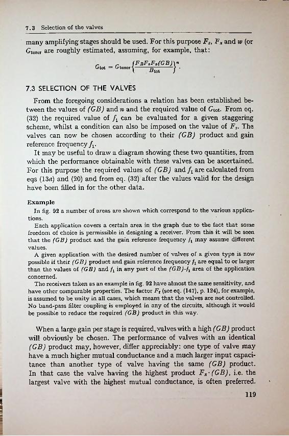
7.3 Selection of the valves
many amplifying stages should be used. For this purpose Fs, Fx and w (or Gtuner are roughly estimated, assuming, for example, that:
Gtot = Gtuner ^FnFsFxfGB^nBtot
7.3 SELECTION OF THE VALVES
From the foregoing considerations a relation has been established between the values of (GB) and n and the required value of Gtot. From eq. (32) the required value of fx can be evaluated for a given staggering scheme, whilst a condition can also be imposed on the value of Fs. The valves can now be chosen according to their (GB) product and gain reference frequency fv
It may be useful to draw a diagram showing these two quantities, from which the performance obtainable with these valves can be ascertained. For this purpose the required values of (GB) and fx are calculated from eqs (13a) and (20) and from eq. (32) after the values valid for the design have been filled in for the other data.
ExampleIn fig. 92 a number of areas are shown which correspond to the various applica
tions.Each application covers a certain area in the graph due to the fact that some
freedom of choice is permissible in designing a receiver. From this it will be seen that the (GB) product and the gain reference frequency fx may assume different values.
A given application with the desired number of valves of a given type is now possible if their (GB) product and gain reference frequency fx are equal to or larger than the values of (GB) and fx in any part of the (GB)-fx area of the application concerned.
The receivers taken as an example in fig. 92 have almost the same sensitivity, and have other comparable properties. The factor Fr (see eq. (147), p. 124), for example, is assumed to be unity in all cases, which means that the valves are not controlled. No band-pass filter coupling is employed in any of the circuits, although it would be possible to reduce the required (GB) product in this way.
When a large gain per stage is required, valves with a high (GB) product will obviously be chosen. The performance of valves with an identical (GB) product may, however, differ appreciably: one type of valve may have a much higher mutual conductance and a much larger input capacitance than another type of valve having the same (GB) product. In that case the valve having the highest product Fx • (GB), i.e. the largest valve with the highest mutual conductance, is often preferred.
I 119'
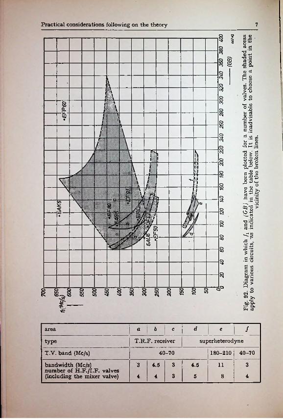
Practical considerations following on the theory 7
a asi|S,
H £1/3 Oo> o | O
°3u rt <U VI3 >
8(*)
sio3
' R45 '»! A 8rvu_'
cn80- 8
\iU5 I •-e-5i 8V* p rt«.9d.S« VI
o-
r< o/<N
/—— ORR> n 'a > d o p o
SS-gVi§■§1 .0 +-
) I I< §4*. nN » I» !! O—ii +1i4 a/\ ^f- J/ §• \ iii£5 r- C
•a *3‘s'g >
■gB§.S
8xiw \* pi■■ ijI §H7-io :g IQJ
8' & S ik 1§(j
\ ml£2W\:- ■a •^38T~ o ^/f5r/ *1.9-S
P SS O g>‘g
8o
8PcP oono 8 § §§ 8 8 8 8K 5)_ io io C5 ciC3 >,
bh £<E &f
'Cr
“ | 4 | c i I /d earea
superheterodyneT.R.F. receivertype
i 40-70T.Y. band (Mc/s) 40-70 180-210
3 3bandwidth (Mc/s) number of H.F./I.F. valves (including the mixer valve)
34.5 4.5 11
34 44 5 8
7.3 Selections of the valves
Very large valves, however, are less suitable for these applications, due to the ollowing facts.(a) The gain reference frequency of a large valve is as a rule compara
tively low. Particularly at high frequencies there is then a risk that the maximum gain per stage will no longer be limited by the (GB) product but by the gain reference frequency fv The influence of the input capacitance of the valve on fx may be explained by as follows.
Assume for the sake of simplicity that
gi PH CO2 LkCgykSk ,and
W 4Since the cathode connection is substantially independent of the
choice of Cgu. and Sk, Lk may be taken to be constant. Hence:
constant • Cfflk~ll>.1, PH
(b) Beyond a given limit the value of Fx increases but little with the mutual conductance of the valve, whereas the increase in physical dimensions, price and current drain becomes quite considerable.
(c) Fx has an optimum value above which the total gain begins to decrease with increasing value of Fx. This optimum value of Fx of a particular amplifier depends on various factors: in the first place on the question whether the amplifier operates on a frequency above or below /0 and /„', in other words whether the maximum gain of each stage is limited by or by (GB).
As shown on p. 12, one of the two following conditions usually applies:(1) the signal frequency is lower than /„ and /0', or(2) the signal frequency is lower than /„ but higher than /0' (in this case the
receiver is usually provided with a tuner with additional H.F. amplifying valves).In the first case Fx can be evaluated in the following way: Assume that
CxbCi and x =a = Ci+Co’Ci + Co’ Cx
where Cx denotes the stray capacitance of each I.F. stage and Cy is the stray capacitance of the input circuit. The gain is then proportional to
r-crtfc+. -1/.(Ci + Cy)-'U • (l + Cx (1 + x)-n = X.Ci 4" Co
121
Practical considerations following on the theory 7
When x is varied at constant values of a, b and Cx, X will be the maximum at
dA'-z— = 0, or d xUX nX
= 0,ax -}- bx2 1+xwhence
± . (i _ M , 1X+JL2b \ 2n) ^ \ 462 \ 2n) ^ 2bn '*opt —
If a is given a value between 0.5 and 0.7 and b is from 0.5 to 1, whilst the number of stages n may vary between 3 and 8, the value of A'0pt will be from 0.095 to 0.04, which gives for Fx = 1/(1 + x), a value of 0.92 to 0.96.
When the circuits are coupled by band-pass filters the results are very similar.
It can be shown in an analogous way that, when a tuner is used, the larger I.F. gain due to a further increase of the dimensions of the I.F. amplifying valves is outweighed by the smaller gain of the tuner. The optimum value depends on the design of the tuner and the valves with which it is equipped. As a rule little is gained by choosing larger valves than correspond to Fx = 0.8.
7.4 STAGGERED TUNING SYSTEMThe (GB) product and the value of n having been determined, a detailed
staggered tuning system can now be worked out, from which the values of Fb, Fs and Fx and the performance of the amplifier can be determined with greater accuracy.
In designing this tuning system it should be taken into account that it will usually be necessary to incorporate a number of traps to eliminate certain undesired signals originating from adjacent channels and the sound channel of the wanted transmission.
As can be seen from the response curve shown in fig. 91, the attenuation of these signals by the H.F. and I.F. circuits is inadequate: the required additional attenuation is given by the difference between this curve and the desired response curve.
The incorporation of a trap also affects the response curve on either side of the frequency which has to be suppressed; the greater the attenuation, the more serious is the influence on the response curve. To evaluate the influence of the traps1), the following two quantities must be calculated:(1) The relative quality factor r, i.e. the ratio Qt/Q of the quality factor
of the trap to that of the circuit to which it is connected.(2) The separation s, i.e. the relative detuning of the trap with respect
x) J. Avins, Electronics, Jan. 1950.
122
7.4 Staggered tuning system
to the circuit, multiplied by the quality factor Qt of the trap, viz.:
,_(««_ 2s) fll_Wo «</ (146)
where cand co0 are the resonant frequencies of the trap and of the circuit respectively.
The values of r and s having been determined, the changes to which the response curve is subject at a given attenuation can be derived from one of the graphs given in figs 113a to l of Appendix I.
These graphs are based on the theory of detuned band-pass filters with two resonant circuits and can be derived from the response curves of four single circuits whose quality factors and resonant frequencies are related to the properties of the circuit and the trap and their mutual coupling.
The changes to which the response curve is subject as a result of the presence of traps must be corrected when these lie within the pass band range of the video signal. This is achieved by sligthly changing the tuning and damping of the I.F. circuits. The effects of these modifications can be determined by means of figs 113m and n of Appendix I.
The influence of the traps cannot be neutralized completely over the entire pass band. This is not objectionable, since the purpose in view is only to obtain an acceptable response curve which gives a satisfactory step function.
It is further of interest to investigate to what extent the corrected response curve is situated above or below the original curve. As a rule the differences will be small, so that the total gain is hardly affected by the incorporation of traps.
It is now possible to design a corrected staggered tuning system. In the corresponding diagram the top extremities of the perpendiculars no longer coincide with the points dividing the semi-circle into equal parts, as is the case in fig. 8. The tunings and dampings of the various circuits are now exactly known and so are the tunings of the traps and the tightness with which they are coupled to the circuits. It is therefore possible to determine the total capacitance Cx of the circuit and consequently the value of Fx with greater accuracy.
It is now necessary to ascertain whether the staggered tuning system chosen can indeed be achieved without any of the stages operating at a frequency exceeding /0. If this is not possible, additional capacitance will have to be added to the stage concerned in order to reduce the bandwidth of that stage sufficiently. In this case, however, the gain of this stage will also be reduced owing to the low'er value of Fx.
■
i
;i
IIii
i
ii.•'!I
: i
iiii. !!
II
:.
iH
It!
123
• •'
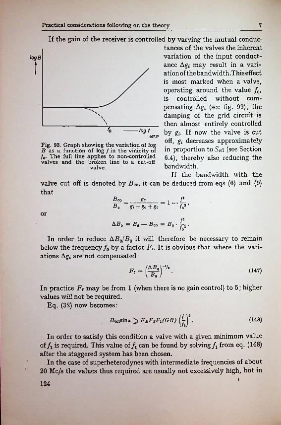
Practical considerations following on the theory 7
If the gain of the receiver is controlled by varying the mutual conductances of the valves the inherent variation of the input conductance Agi may result in a variation of the bandwidth.This effect is most marked when a valve, operating around the value /0, is controlled without corn-
top#
i
pensating A gi (see fig. 99); the damping of the grid circuit is then almost entirely controlled by gi. If now the valve is cut off, gi decreases approximately
f0 log f66739
Fig. 93. Graph showing the variation of log . . „ .£ as a function of log / in the vinicity of in proportion to ocff (see bection/0. The full line applies to non-controlled 6.4), thereby also reducing the valves and the broken line to a cut-off '
valve. bandwidth.If the bandwidth with the
valve cut off is denoted by BCo, it can be deduced from eqs (6) and (9) that
Bco /2Sc=1-/>B0 gi + go+gc
or
b«'/7-In order to reduce A B0[B0 it will therefore be necessary to remain
below the frequency /0 by a factor FT. It is obvious that where the variations A gi are not compensated:
A B0 — B0 — B co —
-($P- (147)Ft
In practice Fr may be from 1 (when there is no gain control) to 5; higher values will not be required.
Eq. (32) now becomes:
Ptotsina ^ FbFxFt(GB) (LJ. (148)
In order to satisfy this condition a valve with a given minimum value of fx is required. This value of fx can be found by solving fx from eq. (148) after the staggered system has been chosen.
In the case of superheterodynes with intermediate frequencies of about 20 Mc/s the values thus required are usually not excessively high, but in
\124
7.4 Staggered tuning system
the case of T.R.F. receivers it may be found that no valves are available which have the required value of fv In that case the design may be adapted to the requirements thus imposed by one of the following means:
(1) Reduction of Fr. This may be achieved by improving the compensation of Agi or by not controlling those valves the grid circuits (and possibly the anode circuits) of which have a narrow bandwidth.
As a rule not only Ag; but also AC; will be compensated. For this purpose a resistor Rk shunted by a capacitor C*' must be incorporated in the cathode lead (see Section 6.4.4.).
It follows from eq. (137c) that for compensating ACglk the following condition must be satisfied:
ACjjik
~C^"Skmnx Rk m
denotes the maximum cathode transconductance. Thewhere S/.•maxrequired value of Rk is therefore determined within certain limits. The most favourable value can best be ascertained experimentally.
The required value of Ck' can be calculated from eq. (136/). First the relatively small correction due to SkRk in the denominators isdisregarded, which gives:
gi & gfj 1 + Oi2Cgik2Rk + <*2CgikLkSk — ^CgikCk'SkRk- + gT .
gi no longer varies with Sk when
g-z + <t}~CgikLkSkm&x *** <A2CgikCk'SkmAxRk“ ,
which may be written as:
CgikSkmaxg- + gt &
orCgikSkmax{gt 4~ gz)
Ck' « co2ACgik2
The most suitable value of Ck is again determined experimentally. The resulting input conductance will now be approximately:
gi ** ggi + o>-Cgik2Rk,
or, after substitution of the optimum value of Rk:
<AzCgik&Cgik _Skmax gn + gi*gi « gn +
125i
;■
-
i
Practical considerations following on the theory 7
The second term of this expression may be estimated from:
The loss of gain due to the compensation is approximately:
_________^____1 ■+■ Skm&xRk Cgi k ~b A Cgxk
except in those cases where Rk has such a high value that the mutualconductance is reduced by the resulting grid bias. On the other hand,Fx is slightly improved because the input capacitance of the valvewill now be about equal to the cut-off value of Ct- throughout thecontrol range.
(2) Choice of a more suitable staggered tuning system, with larger values of sina. In such a system Fb will usually be smaller, so that the bandwidth Br of the reference circuit may have to be increased considerably. The extreme values between which the gain reference frequency fx thus required may be varied are given on the one hand by (n -j- 1) synchronous circuits and, on the other hand, by a flat staggered (n -f- I)tuple.
When these changes have been made it will be obvious that, due to the increase of Br, a higher (GB) product is required in order to obtain the same total gain Gtot.
(3) Rendering the most critical circuit less sensitive to Ag, variations. This may be achieved by increasing the damping across the circuit and adding extra capacitance. The advantage of this method is that the circuit also becomes less sensitive to variations of the input capacitance of the controlled valve, but on the other hand the gain decreases so, that valves with a higher (GB) product are required to obtain the same gain. As a rule, however, there is no need to apply this method to all stages, so that the required increase of the (GB) product is less than the required decrease of the gain reference frequency fv
When the staggered tuning system has been chosen and the gain per stage has been calculated according to Section 7.2, it still remains to be investigated whether the gain is permissible with a view to stability. For each stage eq. (128a) applies, namely:
. (Jj_Y ( Cgik V\(GB)J \Ci + Co)gt'agi-
1Fs > 0.75,
^ ph Vsina/jsina/1+i j/^ .Ghmux
It has been shown in Section 6.3.2 that, in order to avoid irregular-
126
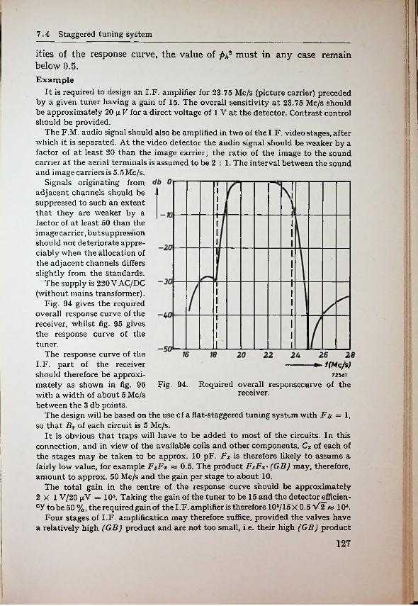
7.4 Staggered tuning system
ities of the response curve, the value of p]i2 must in any case remain below 0.5.Example
It is required to design an I.F. amplifier for 23.75 Mc/s (picture carrier) preceded by a given tuner having a gain of 15. The overall sensitivity at 23.75 Mc/s should be approximately 20 jx V for a direct voltage of 1 V at the detector. Contrast control should be provided.
The F.M. audio signal should also be amplified in two of the I.F. video stages, after which it is separated. At the video detector the audio signal should be weaker by a factor of at least 20 than the image carrier; the ratio of the image to the sound carrier at the aerial terminals is assumed to be 2 : 1. The interval between the sound and image carriers is 5.5Mc/s.
Signals originating from adjacent channels should be suppressed to such an extent that they are weaker by a factor of at least 50 than the image carrier, but suppression should not deteriorate appreciably when the allocation of the adjacent channels differs slightly from the standards.
The supply is 220VAC/DC (without mains transformer).
Fig. 94 gives the required overall response curve of the receiver, whilst fig. 95 gives the response curve of the tuner.
The response curve of the I.F. part of the receiver should therefore be approximately as shown in fig. 96 Fig. 94. Required overall responsecurve of the with a width of about 5 Mc/s between the 3 db points.
The design will be based on the use cf a flat-staggered tuning system with Fn = I, so that Br of each circuit is 5 Mc/s.
It is obvious that traps will have to be added to most of the circuits. In this connection, and in view of the available coils and other components, Cx of each of the stages may be taken to be approx. 10 pF. Fx is therefore likely to assume a fairly low value, for example FSFX fa 0.5. The product FsFx• (GB) may, therefore, amount to approx. 50 Mc/s and the gain per stage to about 10.
The total gain in the centre of the response curve should be approximately 2xl V/20 pV = 105. Taking the gain of the tuner to be 15 and the detector efficien- cy to be 50%, the required gain of the I.F. amplifier is therefore 10S/15X 0.5 V2 104.
Four stages of I.F. amplification may therefore suffice, provided the valves have a relatively high (GB) product and are not too small, i.e. their high (GB) product
!
► f(Mc/s)72561
receiver.
127
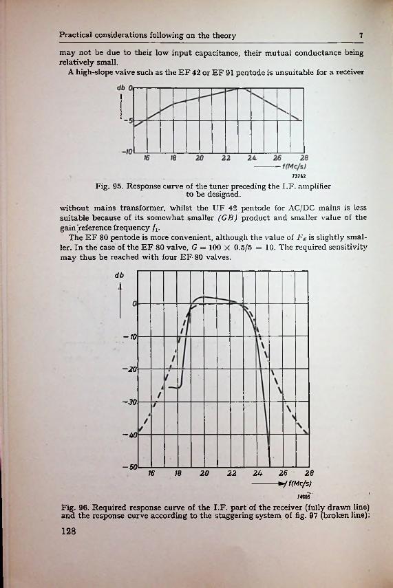
Practical considerations following on the theory 7
may not be due to their low input capacitance, their mutual conductance being relatively small.
A high-slope valve such as the EF 42 or EF 91 pentode is unsuitable for a receiver
73762
Fig. 95. Response curve of the tuner preceding the I.F. amplifier to be designed.
without mains transformer, whilst the UF 42 pentode for AC/DC mains is less suitable because of its somewhat smaller (GB) product and smaller value of the gain reference frequency fv
The EF 80 pentode is more convenient, although the value of Fx is slightly smaller. In the case of the EF 80 valve, G = 100 X 0.5/5 = 10. The required sensitivity may thus be reached with four EF 80 valves.
db
-10
-20
-30
-40
-5016 18 20 22 24 26 28
-----------*if(Mc/s)
74605'
Fig. 96. Required response curve of the I.F. part of the receiver (fully drawn line) and the response curve according to the staggering system of fig. 97 (broken line);
128
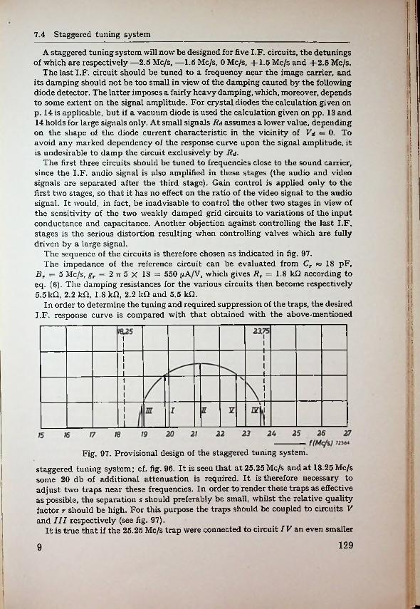
7.4 Staggered tuning system
A staggered tuning system will now be designed for five I.F. circuits, the detunings of which are respectively —2.5 Mc/s, —1.5 Mc/s, 0 Mc/s, +1.5 Mc/s and +2.5 Mc/s.
The last I.F. circuit should be tuned to a frequency near the image carrier, and its damping should not be too small in view of the damping caused by the following diode detector. The latter imposes a fairly heavy damping, which, moreover, depends to some extent on the signal amplitude. For crystal diodes the calculation given on p. 14 is applicable, but if a vacuum diode is used the calculation given on pp. 13 and 14 holds for large signals only. At small signals Rd assumes a lower value, depending on the shape of the diode current characteristic in the vicinity of Vd = 0. To avoid any marked dependency of the response curve upon the signal amplitude, it is undesirable to damp the circuit exclusively by Rd.
The first three circuits should be tuned to frequencies close to the sound carrier, since the I.F. audio signal is also amplified in these stages (the audio and video signals are separated after the third stage). Gain control is applied only to the first two stages, so that it has no effect on the ratio of the video signal to the audio signal. It would, in fact, be inadvisable to control the other two stages in view of the sensitivity of the two weakly damped grid circuits to variations of the input conductance and capacitance. Another objection against controlling the last I.F. stages is the serious distortion resulting when controlling valves which are fully driven by a large signal.
The sequence of the circuits is therefore chosen as indicated in fig. 97.The impedance of the reference circuit can be evaluated from Cr rv 18 pF,
Br = 5 Mc/s, gr = 2 7r 5 X 18 = 550 (zA/V, which gives Rr = 1.8 kfl according to eq. (6). The damping resistances for the various circuits then become respectively 5.5kH, 2.2 kn, 1.8 kfl, 2.2 k£l and 5.5 kH.
In order to determine the tuning and required suppression of the traps, the desired I.F. response curve is compared with that obtained with the above-mentioned
■s.
■
;
I
I
!|
■
t
ii
;■
I; I■ l
|i
i
Fig. 97. Provisional design of the staggered tuning system.
staggered tuning system; cf. fig. 96. It is seen that at 25.25 Mc/s and at 18.25 Mc/s someadjust two traps near these frequencies. In order to render these traps as effective as possible, the separation s should preferably be small, whilst the relative quality factor r should be high. For this purpose the traps should be coupled to circuits V and III respectively (see fig. 97).
It is true that if the 25.25 Mc/s trap were connected to circuit IV an even smaller
j:j:
20 db of additional attenuation is required. It is therefore necessary to
1299
I
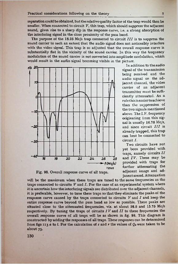
Practical considerations following on the theory 7
separation could be obtained, but the relative quality factor of the trap would then be smaller. When connected to circuit V, this trap, which should suppress the adjacent sound, gives rise to a sharp dip in the response curve, i.e. a strong absorption of the interfering signal in the close proximity of the pass band.
The purpose of the 18.25 Mc/s trap connected to circuit III is to suppress the sound carrier to such an extent that the audio signal does not noticeably interfere with the video signal. This trap is so adjusted that the overall response curve is substantially flat in the vicinity of the sound carrier. In this way the frequency modulation of the sound carrier is not converted into amplitude modulation, which would result in the audio signal becoming visible in the picture.
db 20In addition to the audio
signal of the transmission being received and the audio signal on the adjacent channel, the video carrier of an adjacent transmitter must be sufficiently attenuated. As a rule this is easier to achieve than the suppression of the two signals mentioned above. The I.F. frequency originating from this signal is usually 16.75 Mc/s, and since circuit III is already trapped, this trap can best be connected to circuit I.
Two circuits have not yet been provided with traps, namely circuits II and IV. These may be provided with traps for further attenuating the adjacent image and adjacent sound. Attenuation
will be the maximum when these traps are tuned to the same frequencies as the traps connected to circuits V and I. For the case of an experimental system where it is uncertain how the interfering signals are distributed over the adjacent channels, it is preferable, however, to tune these traps so that they eliminate the peaks of the response curve caused by the traps connected to circuits V and I and keep the entire response curve beyond the pass band as low as possible. These peaks are situated close to the attenuated frequencies, viz. at about 26.5 and 15.75 Mc/s respectively. By tuning the traps of circuits IV and II to these frequencies the overall response curve of all traps will be as shown in fig. 98. This diagram is constructed by adding the responses of all traps. These responses can be determined from figs 113 a to /. For the calculation of s and r the values of Q8 were taken to be about 75.
-10
-20
-30
-4016 18 20 22 2U 26 28
-----------► f(Mc/s)72565
Fig. 98. Overall response curve of all traps.
130
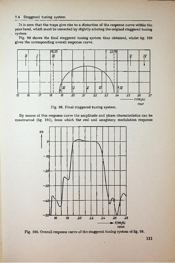
7.4 Staggered tuning system
It is seen that the traps give rise to a distortion Of the response curve within the pass band, which must be corrected by slightly altering the original staggered tuning
. system.Fig. 99 shows the final staggered tuning system thus obtained, whilst fig. 100
gives the corresponding overall response curve.
72567Fig. 99. Final staggered tuning system.
By means of this response curve the amplitude and phase characteristics can be constructed (fig. 101), from which the real and imaginary modulation response
----------- ► f(Mc/s)72568
Fig. 100. Overall response curve of the staggered tuning system of fig. 99.
131
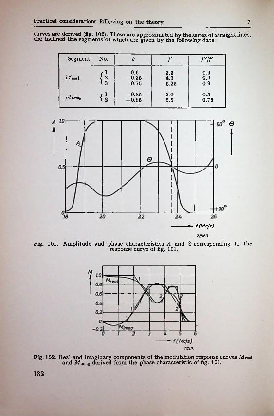
Practical considerations following on the theory
curves are derived (fig. 102). These are approximated by the series of straight lines, the inclined line segments of which are given by the following data:
7
Segment No. h nrr
{2 0.6 0.G3.3Mreal —0.35 4.3 0.9
0.75 0.95.25
1 —0.85 -f 0.85
3.0 0.5{mag 2 0.755.5
0
--------- ► f(Mc/s)
72569
Fig. 101. Amplitude and phase characteristics A and 0 corresponding to theresponse curve of fig. 101.
72570
Fig. 102. Real and imaginary components of the modulation response curves Mreal and Mimag derived from the phase characteristic of fig. 101.
132
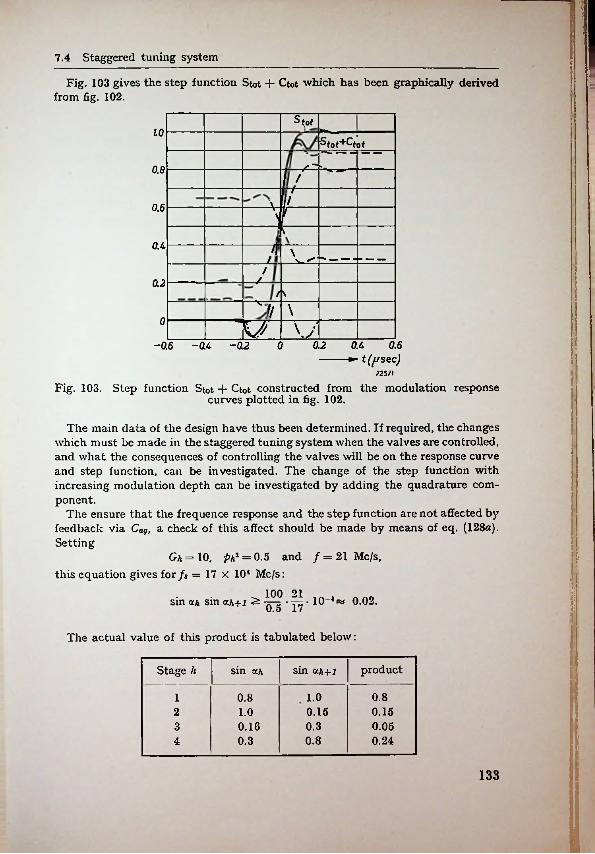
17.4 Staggered tuning system
Fig. 103 gives the step function Stot + Ctot which has been graphically derived from fig. 102.
stot1.0
sfot+ctot
0.8 /A/A0.6 '\
0.4 ~n \ ^L/
J-0.2/ \
V
\li0 v7
0 0.2 0.4 06------- ~t(jjse c)
72571
Fig. 103. Step function Stot + Ctot constructed from the modulation responsecurves plotted in fig. 102.
-0.6 -04 -02■
The main data of the design have thus been determined. If required, the changes which must be made in the staggered tuning system when the valves are controlled, and what the consequences of controlling the valves will be on the response curve and step function, can be investigated. The change of the step function with increasing modulation depth can be investigated by adding the quadrature component.
The ensure that the frequence response and the step function are not affected by feedback via Cag, a check of this affect should be made by means of eq. (128a). Setting
!Gh = 10. ph2 = 0.5 and / = 21 Mc/s, this equation gives for/s = 17 X 104 Mc/s:
sin oca sin cca+2 ^ • 10-4« 0.02.
The actual value of this product is tabulated below:
productsin oca+2Stage h sin oca
0.80.8 1.010.15 0.152 1.00.3 0.053 0.160.80.3 0.244
133
I
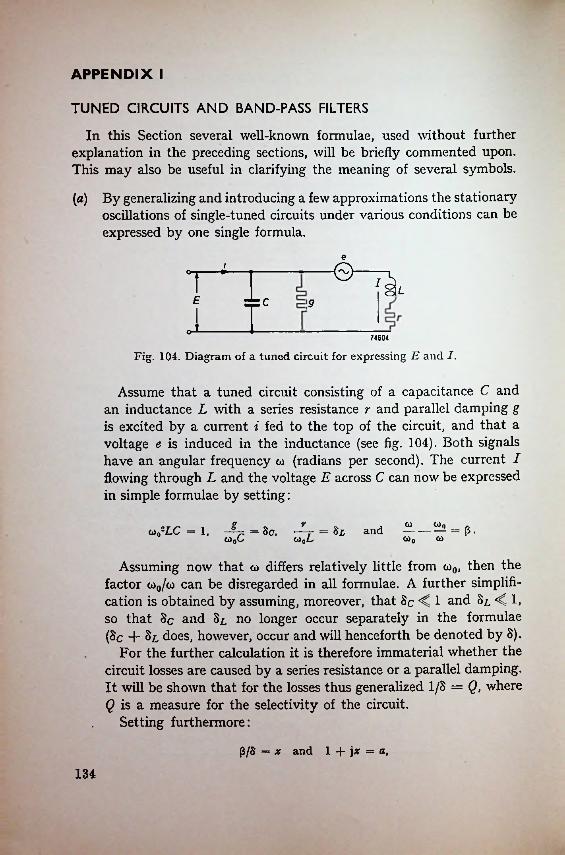
APPENDIX I
TUNED CIRCUITS AND BAND-PASS FILTERS
In this Section several well-known formulae, used without further explanation in the preceding sections, will be briefly commented upon. This may also be useful in clarifying the meaning of several symbols.
(a) By generalizing and introducing a few approximations the stationary oscillations of single-tuned circuits under various conditions can be expressed by one single formula.
0—rs ok7
E \9
J74604
Fig. 104. Diagram of a tuned circuit for expressing E and I.
Assume that a tuned circuit consisting of a capacitance C and an inductance L with a series resistance r and parallel damping g is excited by a current i fed to the top of the circuit, and that a voltage e is induced in the inductance (see fig. 104). Both signals have an angular frequency co (radians per second). The current I flowing through L and the voltage E across C can now be expressed in simple formulae by setting:
Assuming now that co differs relatively little from co0, then the factor &>0/co can be disregarded in all formulae. A further simplification is obtained by assuming, moreover, that Sc K 1 and SlK 1, so that Sc and Sc no longer occur separately in the formulae (Sc + does, however, occur and will henceforth be denoted by 8).
For the further calculation it is therefore immaterial whether the circuit losses are caused by a series resistance or a parallel damping. It will be shown that for the losses thus generalized 1/8 = Q, where Q is a measure for the selectivity of the circuit.
Setting furthermore:
sw0 w
andw02LC = 1, -2^ = Sc,w0G
P/S = x and 1 + j x = a,134
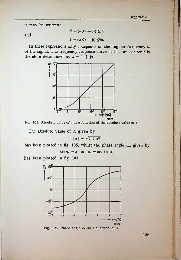
Appendix I
it may be written:E = (<o0Lz — je) Q/a,
I = {<*)0Ce — ji) Q/a.
In these expressions only a depends on the angular frequency <o of the signal. The frequency response curve of the tuned circuit is therefore determined by a = 1 + ]x.
lol 1(fi
and
;:
I Ii;
t
n
io~] i io ioz io3 iou ------- -- I*M*3Q|
72573Fig. 105. Absolute value of a as a function of the absolute value of x.
IThe absolute value of a, given by
| a i = vr+~A*has been plotted in fig. 105, whilst the phase angle c?a, given by
tan (pa = x or <pa = arc tan x,
:ii
Ihas been plotted in fig. 106.
::
]ii
j-i:
Fig. 106. Phase angle as a function of x.
135
c
«
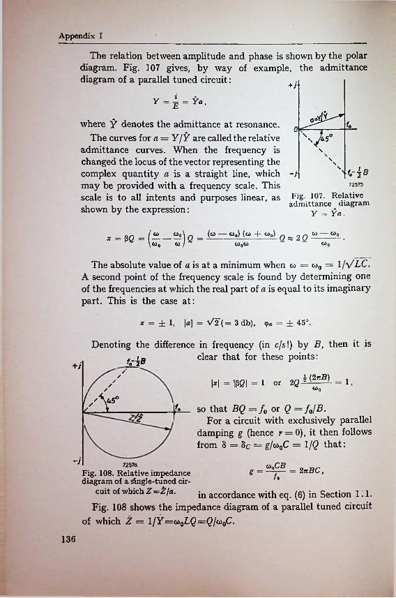
Appendix I
The relation between amplitude and phase is shown by the polar diagram. Fig. 107 gives, by way of example, the admittance diagram of a parallel tuned circuit: +/■
»y=2 = ya.
where Y denotes the admittance at resonance. fo
\The curves for a=Y/Y are called the relative
admittance curves. When the frequency ischanged the locus of the vector representing thecomplex quantity a is a straight line, which -/may be provided with a frequency scale. Thisscale is to all intents and purposes linear, as FiS- 107- Relative , . . r r admittance diagramshown by the expression: y — Ya
72575
Wo <*>/(<o — 0>o) (fa) + Op)
w0COpCO
The absolute value of a is at a minimum when o> = co0 = l/VLC. A second point of the frequency scale is found by determining one of the frequencies at which the real part of a is equal to its imaginary part. This is the case at:
dbl, M = V2 (= 3 db), 9« = ± 45°.
Denoting the difference in frequency (in c/s\) by B, then it isclear that for these points:
X =
!dB+j
W-IMI-1 °r 20ii^- =CUp
1.✓
i/Y1U— SO that BQ =/0 or Q =f0/B.
For a circuit with exclusively parallel damping g (hence r = 0), it then follows from 8 =■8c = g/<*0C = l/Q that:
-y <o0 CB g~~
72576Fig. 108. Relative impedance diagram of a single-tuned cir
cuit of which Z =Zfa.
= 2tt BC,
in accordance with eq. (6) in Section 1.1. Fig. 108 shows the impedance diagram of a parallel tuned circuit
of which Z — l/Y=u)0LQ=Q/<i)0C.
136
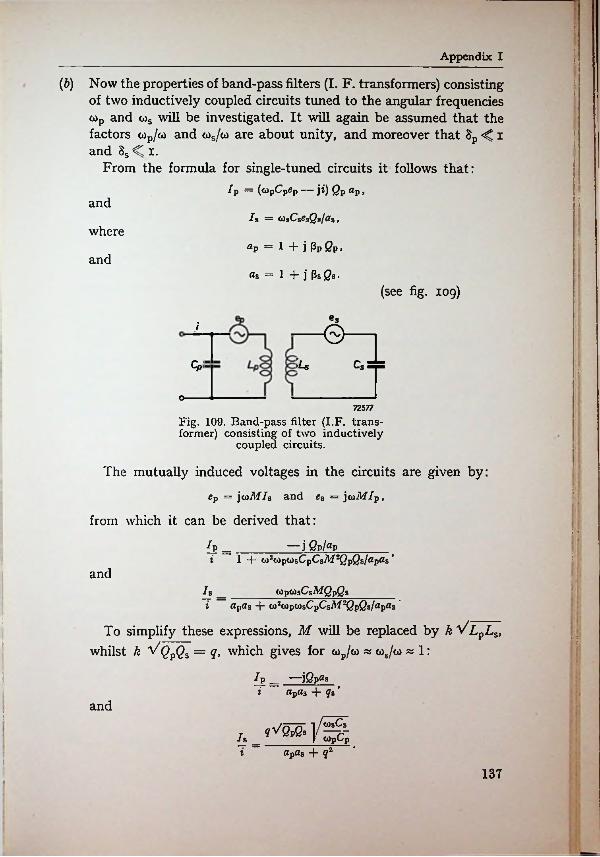
:Appendix I !(b) Now the properties of band-pass filters (I. F. transformers) consisting
of two inductively coupled circuits tuned to the angular frequencies cop and ws will be investigated. It will again be assumed that the factors cop/w and cos/co are about unity, and moreover that Sp i and $s ^ i.
From the formula for single-tuned circuits it follows that:7p = (<opCp5p — j i) Qp cLp,
i
;
.
andIs — OisCsSsQs/ds ,
whereap = l + j Pp Qp,
and«s = 1 4“ j Ps Qs ■
(see fig. 109)
es
Oi
Cp >U ;
o-72577
Fig. 109. Band-pass filter (I.F. transformer) consisting of two inductively
coupled circuits.
The mutually induced voltages in the circuits are given by:
ep = j coM/s and es = joMIp,
from which it can be derived that:
[p _
M
; :—j Qp/gp
T 1 -j- <*hop<*sCpCsM*QpQs/apasand
___________<0p<0sCs.MQpQs________i ctpds + co2cop(OsCpCsM^p0s/«p«s
To simplify these expressions, M will be replaced by k VlpLs, whilst k VQpQs = q, which gives for cop/o) « o)s/co « 1:
Ip __ —j(3pgsi dpCis -j- <7s
Is
■ ■
and
T = apas + q2:137
Appendix I
From= /p
ycoCp£P — /pjwLp
and
£s = = /si“Ls
it is now possible to derive the well-known formulae:
•7. _ -Ep _ wLpgpffs' ~ T ~ ap«3 + q* ~ Zp
^ _ Es _ j<y v'fa>p£pQp<os£sQs _ jff ViP Zs* «p«3 + #2
In analogy with the formula for Zi,
7 7"o — ----------- ; 7 ,«P«s + q-
asaPas + q2
and
flpfls + <?2 '
whilst, moreoverEs£p
(c) The response curves of a band-pass filter consisting of two coupled tuned circuits are given by the denominator of the formula for Zt, viz.:
N = apas -}- q2.
This expression may be written as a product of two factors, both containing an imaginary term j* = jp/S, whilst the real term is independent of the frequency. These factors may, therefore, be regarded as the admittances of two single-tuned circuits which are not coupled1). Hence:
(g + iPO (8* + inN = a a'a" =
Provided the four characteristic quantities S', p', 8" and p" can be determined, the response curve of the band-pass filter can therefore be derived from the so-called ^-diagram of a single-tuned circuit. For this purpose it is assumed that:
P = £ (Pp + Ps). & = \ (8p + 8S), i (Pp — Ps). I — £ (8p — 8s), andm =
w = y*2 — /2 +B. D. H. Tellegen, Coupled Circuits, Philips Research Reports 2, p. 1, 1947
138
-
liAppendix I
It is possible to carry out the following calculations:
V'+Y i + «^ w* ’
y — wand
s = w j/— 1 + j/ i + 5?.w*
Now:= p + = 0 — y, 8' = 8 T e and 8" = 8 ± s ,
in which the upper sign applies when Im is positive.For the further calculation of N the product of the standardized
admittance curves of both fictitious circuits is determined. This product then has to be multiplied by the factor
8'8"8p$s
When the primary and secondary circuits are tuned to the same frequency, s becomes zero, so that 8' = 8" = £ (Sp + Ss). Both fictitious circuits then have the same value of Q, which results in the response curve becoming symmetrical. This curve is then identical to that of two circuits connected in cascade having the same value of Q and an equally large but opposed detuning Af— ± \Wk-—l2 with respect to the resonant frequency. From the above formulae it follows that this detuning is determined by Sp, Ss and k. It is clear that at Sp = 0, Ss and k can be so chosen that the detunings and dampings of the fictitious circuits correspond to the values required for fiat staggering. It is on this principle that the stagger damping system is based by making 8'= |8S= (sin ah)/Qr and k = 1 /Q, which gives:
!
.
;
f_ . V1—sin2 <y.h = ± £ Br cos a/t *±2Qr
(d) The case where the primary and secondary circuits are tuned to the same frequency will now be investigated. Assuming that
Qs/Qv = r and x = (3 V0p0s,
ap = 1 + and as = 1 + )x Vr .Vr
|
i5
then:
ISThis gives:jyVipis I J
= ; II+ ^ + jWVr +1
I j
139
> |
Appendix I
(The expression Vr + may also be written: j/2 + -y + r.)
Eq. (61) can now be deduced directly by setting:
Zp = Rp and Zs — Rs •
It is moreover seen that
Zi =l+-t + q°-
Vr 1+ \x V'andZsZo =
1 4- j X Vr -\------ ^ .
VrAt resonance
i8 and it = Vipi3 = q VZiZZi = z0 = 0 •1 + ?2
The above considerations yield no practical results when, for example, Qp is infinitely large. In that case:
_ 3 kQpQsV<oaLpLs _ dp a& 4- kzQpQs
j /i/<0 VCpCs *2+jP/0s + (j P)2 '
so that1
Yt - ^ = — ]oik \/CpCs ,
whilst
is Csthat i <Vwhere qs = kQs. Moreover:
z0 = so that Z0 = 0.
(e) The following comments will again be confined to band-pass filters the primary and secondary of which are tuned to the same frequency (tuned I. F. transformers).
The polar diagram of
qVZpZ— = j (1 + <72) ^y = it^t
140
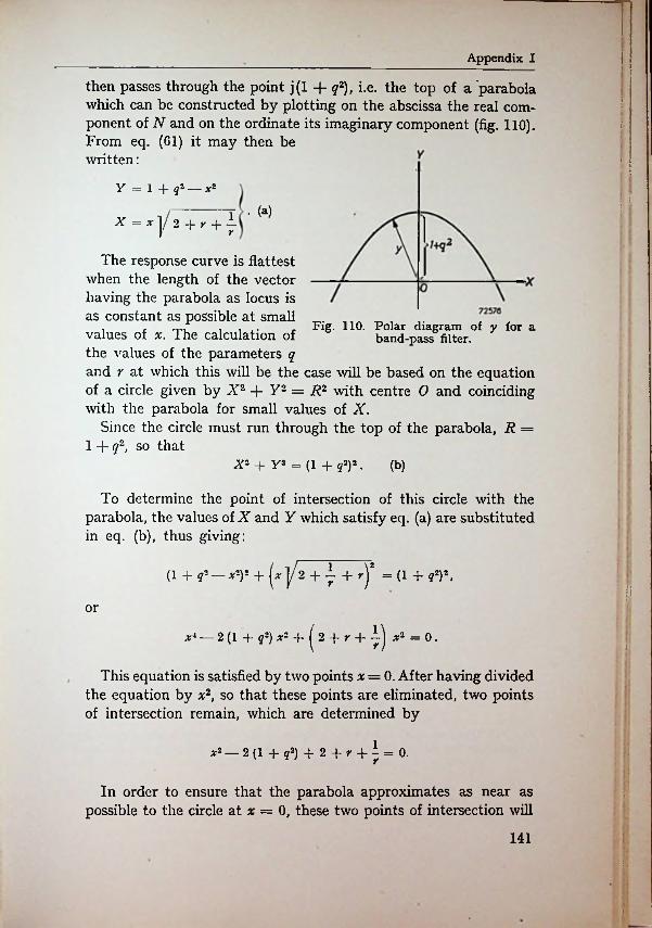
!Appendix I
then passes through the point j(l + q2), i.e. the top of a parabola which can be constructed by plotting on the abscissa the real corn- ponent of N and on the ordinate its imaginary component (fig. 110). From eq. (61) it may then be written: :
y = 1 + q* — *2i
• (a)x =*]/2 + r + j>
The response curve is flattest when the length of the vector having the parabola as locus is as constant as possible at small values of #. The calculation of the values of the parameters q and r at which this will be the case will be based on the equation of a circle given by X2 + Y2 = R2 with centre 0 and coinciding with the parabola for small values of X.
Since the circle must run through the top of the parabola, R = 1 -f- q2, so that
Fig. 110. Polar diagram of y for a band-pass filter.
A'2 + Y2 = (1 + ?2)a. (b)
To determine the point of intersection of this circle with the parabola, the values of X and Y which satisfy eq. (a) are substituted in eq. (b), thus giving:
(*y2 + 7 + 'r-(1 + f2 —**)* + (i + q2)\■
or
x* — 2 (l + q*) xz + ^ 2 + r + ij *2 = 0.I?
This equation is satisfied by two points x = 0. After having divided the equation by x2, so that these points are eliminated, two points of intersection remain, which are determined by
A'2 — 2(1 + ?2) + 2 + * + \ = 0.
In order to ensure that the parabola approximates as near as possible to the circle at x = 0, these two points of intersection will
141
i •
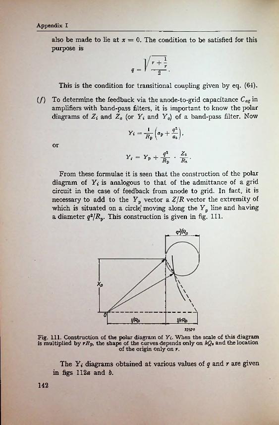
Appendix I
also be made to lie at x — 0. The condition to be satisfied for this purpose is
<7
This is the condition for transitional coupling given by eq. (64).
(/) To determine the feedback via the anode-to-grid capacitance Cag in amplifiers with band-pass filters, it is important to know the polar diagrams of Zi and Z0 (or Y; and Y0) of a band-pass filter. Now
Yi=-i(a-+C)'or
Y- 2TSY< = *
From these formulae it is seen that the construction of the polar diagram of Y» is analogous to that of the admittance of a grid circuit in the case of feedback from anode to grid. In fact, it is necessary to add to the Yp vector a ZjR vector the extremity of which is situated on a circle' moving along the Yp line and having a diameter q2/Rp. This construction is given in fig. 111.
92/RP
Rs '
\
AXp \\\\\
01/Rp VrRp
72579
Fig. 111. Construction of the polar diagram of Yt\ When the scale of this diagram is multiplied by rRp, the shape of the curves depends only on kQs and the location
of the origin only on r.
The Yi diagrams obtained at various values of q and r are given in figs 112a and b.
142
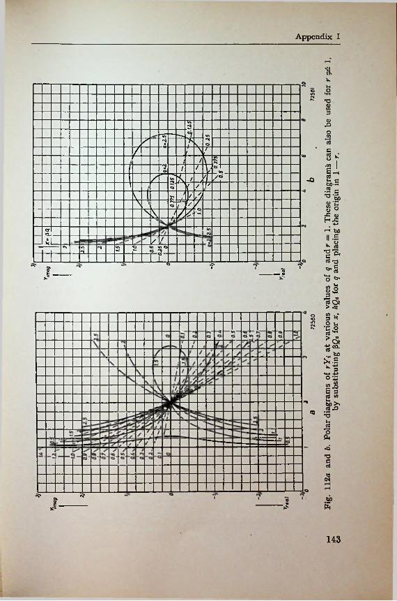
Appendix I
u2 - oS £
<N73oc/53o
N •O
gJO3 757* 7sQ£ \/z >,/ C/
s *■• •£ IC pHcj&.£
•2 c ^•EbsiPIr-5 t/3
<osci
i•3o /
/3IS<s
// -O/ 7// /£ary./3?s: ■3\ /
■h
3crII .£/Ai £
ctf 'O
O ^
i!■a <3
2*♦» 2 m >o o ts ^
■n •N rr8* gJ
> •=;§ H■P
><•£*15SH ■+■»O-J
C/52 ^ £ 3 rt «
o
in<N
<0 313
P-.
73drt
<N
o
" | fcba s.5
143
Appendix I
When the Zi diagram is derived from the Y; diagram a curve is obtained which resembles a cardioid at normal values of q.
If QP is made infinitely large, Y* and Y0 can be expressed in = P& and <7S = kQs, viz.:
+
y0 = ys(l + j,8 + g).The latter locus coincides with the polar diagram of Ys, but when
xs is varied from —c© to +« this line is traversed twice. The minimum values of Y0 are then situated at xs = ± qs.
?s2 ■)
Yi = 1 + j*3and
(g) An interstage circuit provided with a trap may be considered as a double tuned band-pass filter.
When both circuits are tuned to the same frequency (Z* coupling) the response curve can be determined from the Zi diagrams for band-pass filters, but when the tunings are different it is preferable to use the following method, particularly when several circuits of a staggered system are provided with a trap.
First the response curve of the primary circuit without trap is determined. The effect of adding the trap can then be expressed by the attenuation factor at of the trap, that is:
ai = m ■ + ?-.Setting
Q*ps0p = Xi, and p'Qp = s,= rQv
where p' = wp/“8 — "s/«
PpGp = xt — 5 and ps0s = Xt r, >
then, to a good approximation:p >
so that n rq2rx t2
+ xt — s 1 + r-x t2l + y3 xt*l\at\ = 1 + (xt — s)2
The absorption curve of the trap can be graphically determined from the response curves of four circuits by means of the expression
a'a" tfpfls
in agreement with the method outlined in Appendix Ic.
at = a
144
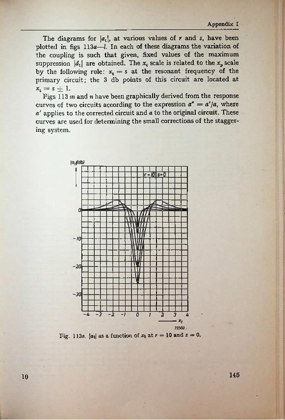
Appendix I
The diagrams for \at\, at various values of r and s, have been plotted in figs 113a—l. In each of these diagrams the variation of the coupling is such that given, fixed values of the maximum suppression |at | are obtained. The xt scale is related to the xp scale by the following rule: xt = $ at the resonant frequency of the primary circuit; the 3 db points of this circuit are located at xt = s ±1.
Figs 113 m and n have been graphically derived from the response curves of two circuits according to the expression an = a'ja, where a' applies to the corrected circuit and a to the original circuit. These curves are used for determining the small corrections of the staggering system.
Fig. 113a. \at\ as a function of xt at r = 10 and s = 0.
14510
i
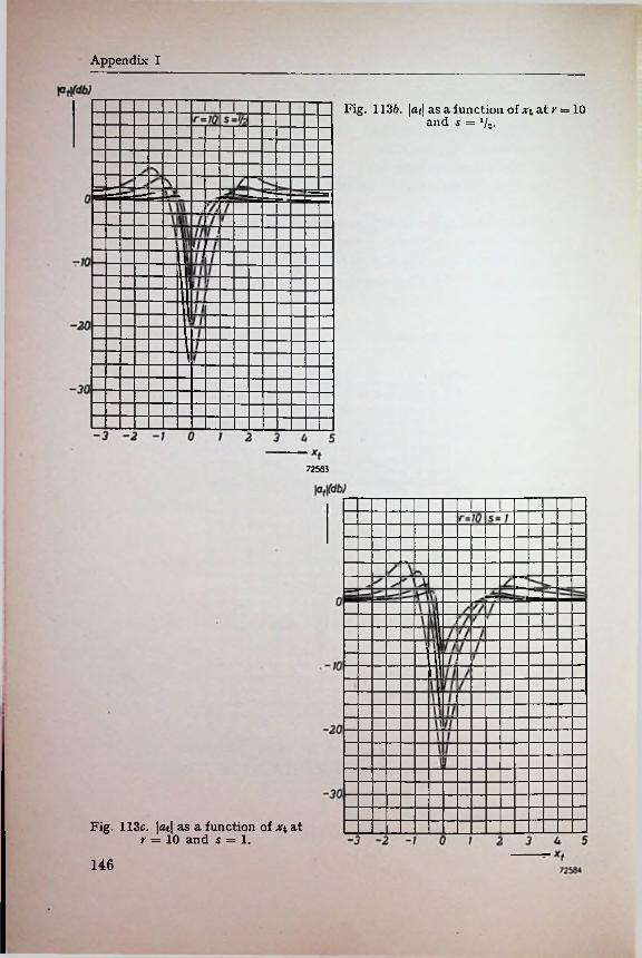
Appendix I
Fig. 1136. |a<| as a function of xt at r = 10and 5 = V-
72583
Fig. 113c. \at\ as a function of xt at r = 10 and 5 = 1.
146
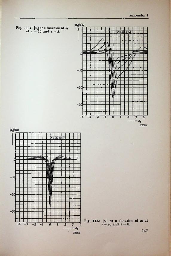
Appendix I
Fig. 113d. |at| as a function of xtat r = 10 and 5 = 2.
Fig. 113c. at as a function of xt at
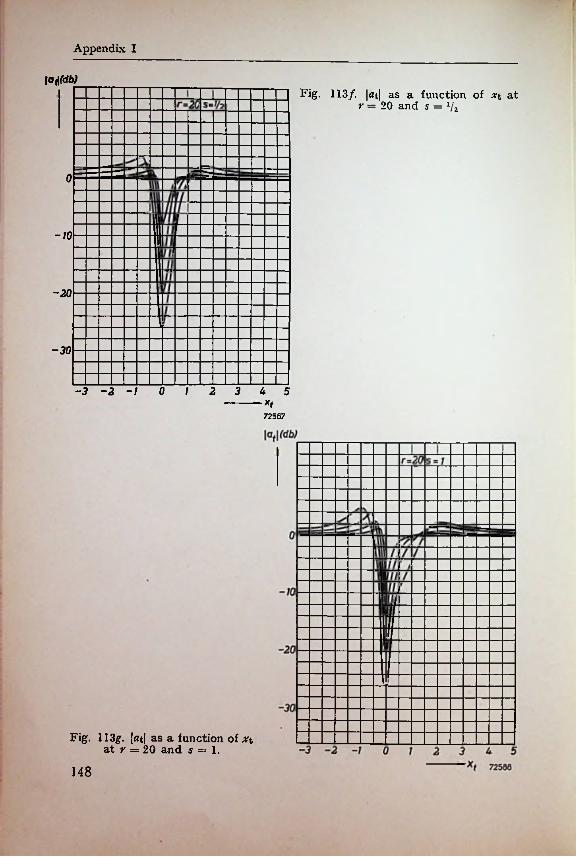
Appendix I
I atfdb)Fig. 113/. |at| as a function of xt at
r = 20 and 5 = 1/a
0
-10
-20
-30
0 12 3 4 5-3 -2 -1
72587
Fig. 113g. \at\ as a function of xt at r = 20 and 5=1.
148
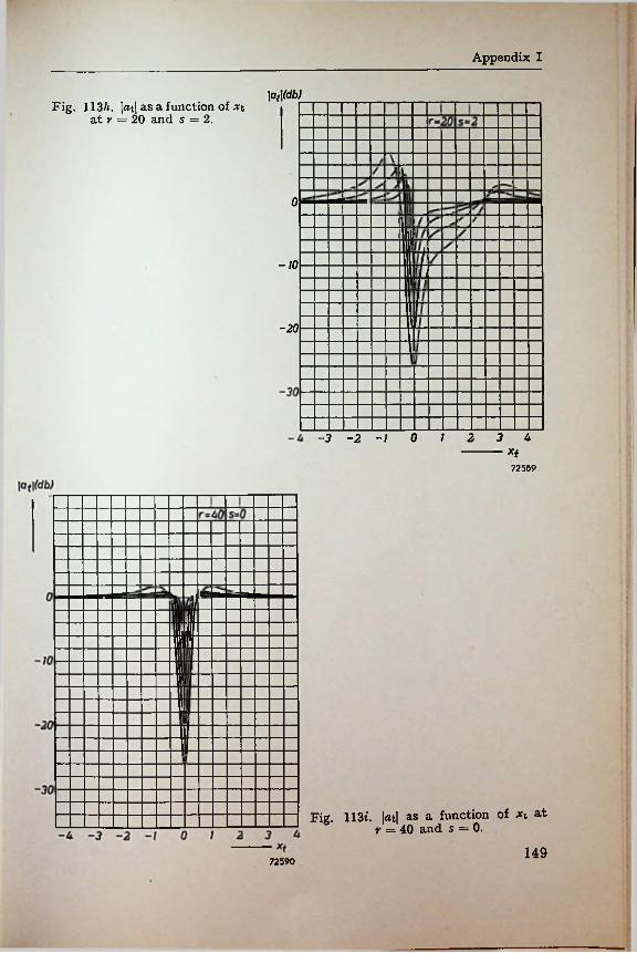
Appendix I
\at\(db)Fig. 113/j. |at| as a function of xt
at r = 20 and 5 = 2.
0
-10
-20
3-2-1 0 1 2 3 b
72569
Fig. 113*. M as a function of Xx. at r — 40 and s = 0.
14972590
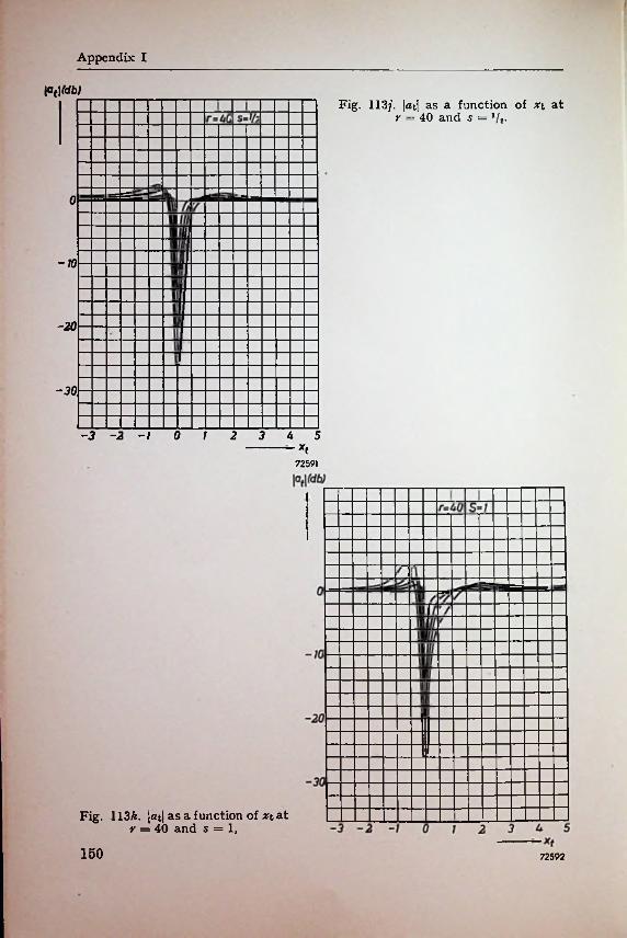
Appendix I
pt\(db)Fig. 113/. |at| as a function of xt at
r = 40 and s = l/t.
0
-10
-20
-30
-3 -2 -1 0 1 2 3 4 5
72591
Fig. 113A. |at| as a function of xt at r = 40 and s = 1,
150 72592
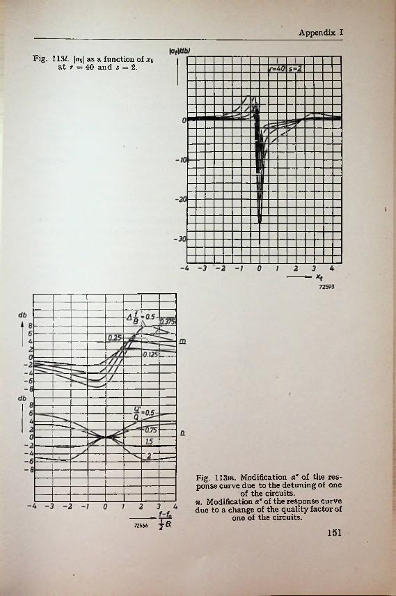
Appendix I
Fig. 113/. |at| as a function of .rtat r — 40 and 5 = 2.
Fig. 113m. Modification a" of the response curve due to the detuning of one
of the circuits.n. Modification a” of the response curve due to a change of the quality factor of
one of the circuits.72566
151
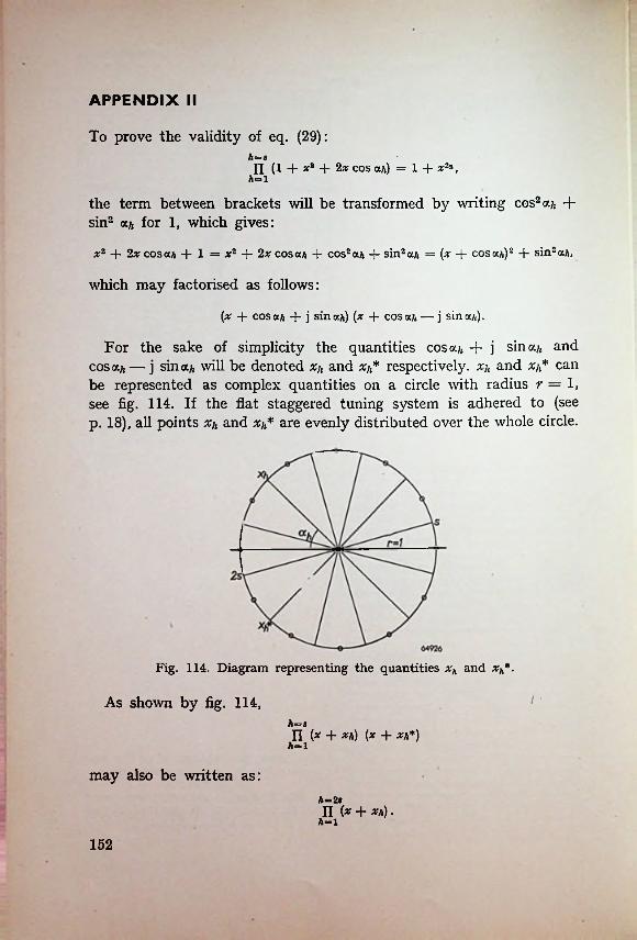
I
APPENDIX II
To prove the validity of eq. (29):
n (1 + *a + 2# cos oca) = 1 + x2*, A= l
the term between brackets will be transformed by writing cos2 a/, + sin2 a/, for 1, which gives:
xz + 2# cos a* + 1 = x2 + 2x cos a a + cos2 oca + sin2 oca = (x + cos oca) 2 + sin2 oca,
which may factorised as follows:
(x + cos oca + j sin cca) (x + cos oca — j sin oca).
For the sake of simplicity the quantities cos a/t -{- j sin ah and cos a/, — j sin a a will be denoted x/t and %h* respectively. %h and Xjt* can be represented as complex quantities on a circle with radius r = 1, see fig. 114. If the flat staggered tuning system is adhered to (see p. 18), all points xjt and xjt* are evenly distributed over the whole circle.
Fig. 114. Diagram representing the quantities xh and xh*.
I •As shown by fig. 114,A=sn (* + Xh) (x + Xh*)
A-l
may also be written as:A-2sn (* + .
1
152
Appendix II
This product can be worked out, giving:7i=2sn (* + xk) = h Eh %2g~h,
28
A-0h*=n.
where E0 — 1,Ex — + x2 -f- • • • x28, andE2 = Xj%2 + xxx3 + ... x2s_1 x25, etc.
Summarizing, En always contains all possible products of n terms xjt.All coefficients of the power series from Ex to are now obviously
zero, since each product, say xp-xq-.. .xr, has a “twin” with opposite sign.
The last term x1 • x2 • ... x2Sl on the other hand, is equal to unity, since for each factor of this product there is again a “twin”, which is now conjugate complex, and as the product of each pair of conjugate complexes is unity, this is also the case with the entire term.
Concluding, only the first and last terms of the whole power series
2s2 Ehx'-*-i'
/i*=0
remain, which gives:A = 2sII {x + *h) = *2S + 1.
A=1
ijj
153
APPENDIX III
(«) A general method for determining the step function from the amplitude response curve is based on the Fourier analysis of the signal. According to the integral theorem of Fourier, a function y(/) may, under certain conditions, be described by:
+ 0°y(0 = J Y(«) dw , (c)
— oo
where eico< stand for cos tot + j sin Y(co) is termed the spectral amplitude of the function y(/), and is given by:
J-OO
Applied to the function B.(t) of eq. (33), this gives:
+ oo
(d)e-j<o* y(/) d/.
ooi + i J
0
1 (e)dco .:
The spectral amplitude of this function is, therefore, l/2~j«.For the function H(/-r), representing a unit step at t = t, the
spectral amplitude is given by e_jWT/27rjco.The Fourier components of the input signal applied thus having
been determined, it is possible to derive from the amplitude response curve the corresponding Fourier components of the output signal, after which the step function can be determined from the latter components.
This principle will now be applied to the envelope of the H. F. signal. The step-like variation of the signal amplitude is analysed into sinusoidal modulation components:
oo
£(=£b+£s(l+I j ^d-). 0
(<)i
After the amplitude and phase of these components have been changed in the amplifier, the following equation applies:
CO
l l r A(«)2tk J ~
o{ * — D (to) |Eo (g)dcosin <o^r = Eh + E3
A(co) and D(o) are determined by the complex modulation response curve M(co). Once M(co) is known, E0/G, i.e. the step
154
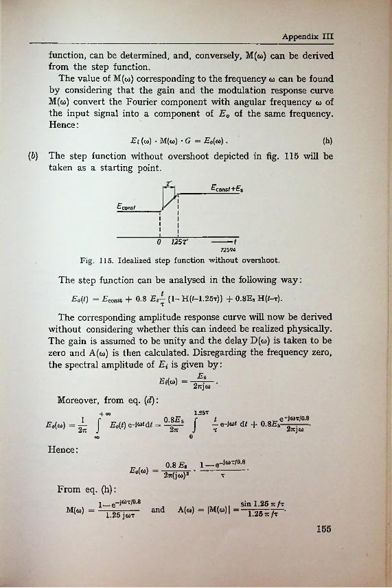
Appendix III
function, can be determined, and, conversely, M(co) can be derived from the step function.
The value of M(co) corresponding to the frequency co can be found by considering that the gain and the modulation response curve M(co) convert the Fourier component with angular frequency co of the input signal into a component of E0 of the same frequency. Hence:
Ei (co) • M(co) • G = -Eo(co) •
(6) The step function without overshoot depicted in fig. 115 will be taken as a starting point.
(h)
Econst +ES
Econst
III
0 125T72594
Fig. 115. Idealized step function without overshoot.
The step function can be analysed in the following way:t
E0{t) = Fconst + O.S Es-{ 1- H(/-1.25t)} + 0.8ES H(/-t).T
The corresponding amplitude response curve will now be derived without considering whether this can indeed be realized physically. The gain is assumed to be unity and the delay D(co) is taken to be zero and A(co) is then calculated. Disregarding the frequency zero, the spectral amplitude of Ei is given by:
Fi(co) = Es27wjcO
Moreover, from eq. (d):1.25T4-co
e -jWT/o.80.8-Es — d/ + 0.8.EsEoW = ~ J E„(i) e-i“< dl = 2ij J ,0
2”jcoeo
Hence:l__ e—jCOT/0.80.8 EsF0(w) =
27t(jtt)2 T
From eq. (h):1 _e-jti)T/0-8
1.25 jcoTsin 1.25 7: /t
1.25 7zfxand A(co) = |M(co)| =M(co) =
155
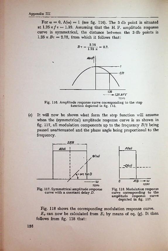
Appendix III
For to = 0, A(co) = 1 (see fig. 116). The 3 db point is situated at 1.25 tc/t = 1.39. Assuming that the H. F. amplitude response curve is symmetrical, the distance between the 3 db points is 1.25 7z jBt = 2.78, from which it follows that:
2.7823t = = 0.7.1.25 tc
A((0)
0.71
1.39--------125 xir
72595
Fig. 116. Amplitude response curve corresponding to the step function depicted in fig. 115.
(c) It will now be shown what form the step function will assume when the (symmetrical) amplitude response curve is as shown in fig. 117, all modulation components up to the frequency Bj2 being passed unattenuated and the phase angle being proportional to the frequency.
2JtBA(co)A(o))
0(0)1/
/ -D(to)/
Aarc tan DI
/ JtB —► w72597
Fig. 118. Modulation response curve corresponding to the amplitude response curve
depicted in fig. 117.
0(i)72596
Fig. 117. Symmetrical amplitude response curve with a constant delay D.
Fig. 118 shows the corresponding modulation response curve. E0 can now be calculated from E{ by means of eq. (g). It then
follows from fig. 118 that:
156
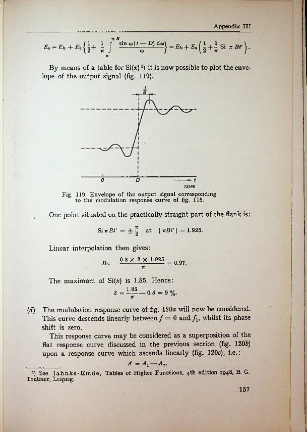
Appendix III
— Bsin o>(l — D) dw}-*,+*(*+!E0 = Eb + Es | 2 +
By means of a table for Si(#)x) it is now possible to plot the envelope of the output signal (fig. 119).
j )■
Si 7T Bt'Oi
o
D072596
Fig. 119. Envelope of the output signal corresponding to the modulation response curve of fig. 118.
One point situated on the practically straight part of the flank is:
SinBt* = ± £ at | -Bt' \ = 1.925.
Linear interpolation then gives:
0.8 X 2 X 1.925 = 0.97.Bt = —
The maximum of Si(x) is 1.85. Hence:
S =-— — 0.5 = 9%.7T
!(d) The modulation response curve of fig. 120a will now be considered. This curve descends linearly between / = 0 and flt whilst its phase shift is zero.
This response curve may be considered as a superposition of the flat response curve discussed in the previous section (fig. 1206) upon a response curve which ascends linearly (fig. 120c), i.e.:
A = Ai — A 2.See Jahnke-Emde, Tables of Higher Functions, 4th edition 1948, B. G.
Teubner, Leipzig.157
;
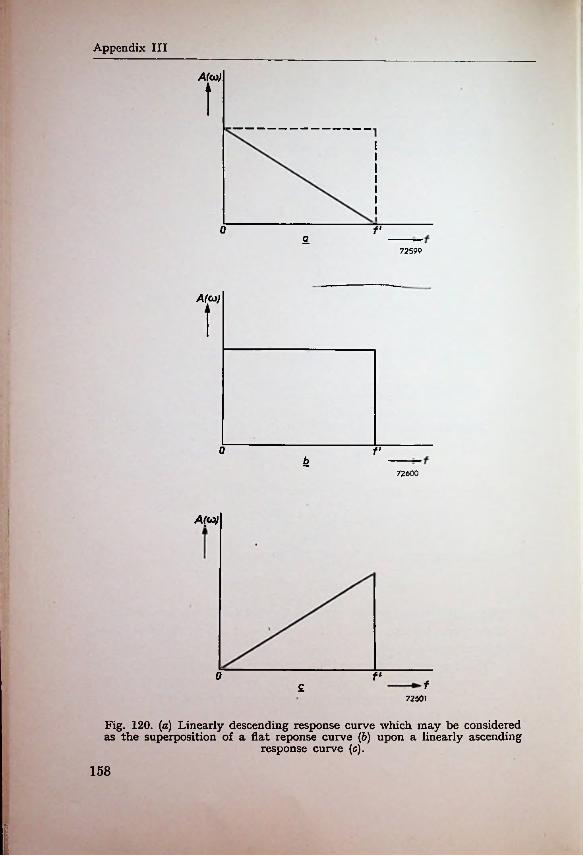
Appendix III
A(<o)
t
0 f2
72599
A(co)\
0 fb
72600
Atto)
0 ff£
72601
Fig. 120. [a] Linearly descending response curve which may be considered as the superposition of a flat reponse curve (6) upon a linearly ascending
response curve (e).
158
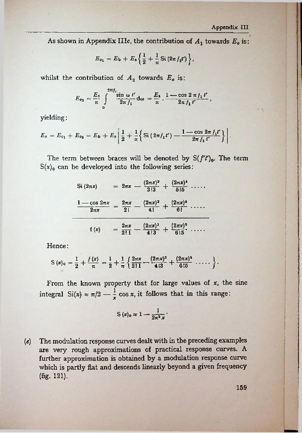
Appendix III
As shown in Appendix IIIc, the contribution of A1 towards E0 is:
£0l = £b + £s{i + isi(2«
whilst the contribution of A2 towards E0 is:27T/|
£-=l J sin to t' , Es 1 — cos 2 - fit'dw = —2txfx —o
yielding:
i + i{si(2,/1/') 1 — cos 2tz fxf}•E0 = Eoi + E0z = Eb + Es2*/i *'
The term between braces will be denoted by S(/T)0. The term S(*)0 can be developed into the following series:
(2tc*)3 , (2 TZX)*Si (2nx) = 2tt* — +3 !3 5!5
(2tc*)3 (2tt*)64! + 6!
1 — cos 2nx 2tzx2!2nx
(2tt*)s(2kx)2kx 3
f (*) +4! 3 6!52! 1 i
Hence:(2kx)z [2tzx)*
413 + 6!51 + /W-i + i/2 ^ it 2 \
From the known property that for large values of x, the sine 7c/2 — i cos x, it follows that in this range:
2nx }•s {x)o = 2! 1
integral Si(*)
1S {x)0 « 1 2tz2x
i(e) The modulation response curves dealt with in the preceding examples
are very rough approximations of practical response curves. A further approximation is obtained by a modulation response curve which is partly flat and descends linearly beyond a given frequency(fig. 121).
f159
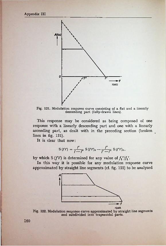
n
Appendix III
s\\\\\A(co) \\
\\\
0 /f" Vf//
72602/////////Fig. 121. Modulation response curve consisting of a flat and a linearly
descending part (fully-drawn lines).
This response may be considered as being composed of one response with a linearly descending part and one with a linearly ascending part, as dealt with in the preceding section (broken lines in fig. 121).
It is clear that now:
V rS (/V) = s (/T)o s (/'0 0 ,
by which S (ft') is determined for any value of fi/fi-In this way it is possible for any modulation response curve
approximated by straight line segments (cf. fig. 122) to be analysed
f—r%
Ai ti
f72603
Fig. 122. Modulation response curve approximated by straight line segments and subdivided into trapezoidal parts.
i:
160:
Appendix IIIinto trapezoidal parts similar to the full-line modulation curve in fig. 121.
It is on this principle that the method of Section 3.4 is based.
response
analysis outlined in
(/) The modulation response curve will again be taken to be flat as far as/i and then suddenly dropping to zero, as was the case in Appendix IIIc, but it will now be assumed that all sinusoidal modulation compents are shifted 90° in phase (imaginary response).
The output step function is then:
27T/i
1
COS CO t'E-z\ Ci (2*/,<').7w
dco =co
By giving the response curve a linearly descending and a linearly ascending part according to fig. 120a, an output step function is obtained which can be calculated to be:
-ti sin (2tc/T) jCi (2tc/T)Es C( /T)* 2 iz/'t
The form C(x)0 can again be transformed into a series:
, 0 (2t:*)2 , (2tt*P (2-x)°Ci (2tt*) = const. + logc 2tzx----- ------- h
(2 izx)* , {2ux)* (2tt*)«
6!6
sin 27xx +l 7!5!3!x
(2-*)*(2tzx)2 (2t:x)*312 + 5!4f (x) = const. + logo x 7!6
Hence:(27t*)2 , (2n*)* (2nJf)«const. + logc x — +C(*)o 7 !65!43 !2
Since, according to the cosine integral tables, Ci(*) « sin x/x at large values of *, in this range C(a;)0 « 0. At very small values of x, C(x)0 and loge approach —<».
When C(ft') diagrams are plotted with a logarithmic time scale they approximate to parallel straight lines at small values of x. In fact, for a trapezoidal component (see fig. 122) of the imaginary response curve:
16111
Appendix III
/' rC (/'/') = C (/r) o c (ro<> =r—r r—rr= C (/r)o + {c(/y)o—c(rno}.r—r
For small values of the second term must assume a finite value, because for small values of ft' the lines C(/Y)0 and C(/Y)0 run parallel. The proof that the output step function has a finite value when the (imaginary) response is zero for /= 0 and /= «*, is based on this property.
For this purpose a step function of the form:
hiC^T) + h2C(/2Y) +h3C(/3T) .......
will be investigated. This step function may be written as:
fix C (AT) +
+ h2 c urn + h2 {c urn - c urn} +
+ h, c urn + {c urn—c urn} •The sum of the left-hand terms of each line is zero because + h2 -f h3 = 0. Since the fines C(/jY), C(f2't')t C(/3T), etc.
run parallel for small values of f't', the forms between the large brackets must assume a finite value for small values of t'. The resultant thus also has a finite value.
162
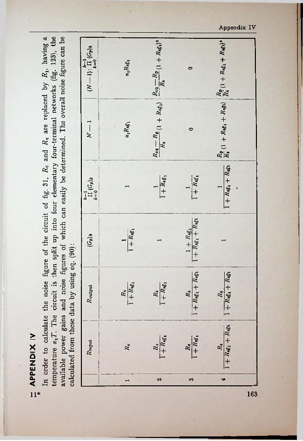
Appendix IVd <u <u
43 rO Cl C-1
bn -M ■mBc aOr d ft!ft!> uCOd ++CSJ Ib?
■** •«:2 *4
*SP435ft! o
H tmbn ft!8a
ft!03 +<vCO I £-a J2 o _ t5 c
XI o _
111 Oi c >
*1 O’
«$Kft!
*5?ft!ftS
2 o +d +<V *52 .2 £ d £ HV-
.1* <u X3* tl ■Sl'l«? 5*!
-+-*- c «1 <U rd
£oft^ ft!&* ft!8 +I *cr
at mft!|0!ft!
d♦J
*I ft!£j i +^tnft!CO £ CU) *
<B+bn r3 +,7< i_i <=>G ii ft!CJ CO
dM3 +I
B !*2 d+j o i30 -2 ,£3 *" c o
• rH • •—<
1 §■*• m
43 ; _ ^a<b +
M- £ o S° CM co
V) 0J
£ c 9 cr ^ &n ^<9 I « bn § *><u .5CO CO O 3
ft! ft!<n co co •’-<
« • 3 c.s.s ■§ -5 o rt -JJ
T30 o w u
1 tS -3 £jbn ^
bJ £3 + 4-• Hft! ft!S' 93
ft!W
ft!93
ft!93
ft;H •-4
*5?§ + + ft!ft! ft!+ +
59ft!
«H I I ^0a 5 +o
ft! ft! 93
ft!ft!■n
8CX A5g< pH
2 S,-o ++ft! ft!a 9 rdS3 13 .§ 2
*S &+z *2 d
o O..X3 3(3 § > H
-*-» d o
LU0.Q. CM CO
<16311*
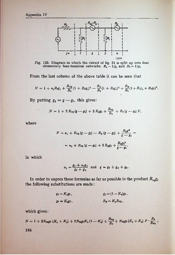
Appendix IV
R^fpO
Rp i
—'UUli
© ft
y'= / 2 3 472604
Fig. 123. Diagram in which the circuit of fig. 31 is split up into four elementary four-terminal networks. Rx = l/gx and Rt = 1/gt.
From the last column of the above table it can be seen that
N = 1 + a1JRsg1 + ^ (1 + RsgiV- — ^ (1 + RsSiy- + ^(1+ nsSl + jRsgo*.RR
By putting gx = g — gt, this gives:
1 + 2 2?Cq (g — gt) + 2 Rpgt + + Rs {g — gt) F,N =
where
RvS2 = g — gtF = <*1 + Rcq {g — gt) — Rp (g — gt) +
Rpgt2= «i + -fteq (g — gt) +2 i^pgt + g—gt'
in which
a — gc + argr 1 gc + gr
and g = gt + gT + gc •
In order to expres these formulae as far as possible in the product Reqgi the following substitutions are made:
gt = (l-Kz)gi,
Rp = K3Rcq ,
gc = K1gi,
gr = Kogi,
which gives:
RsN = 1 + 2i?cqgi (Kx + Kz) + 2RCqgiK3 (l — K2) + ^ + Rcqgi (Kx + KJF-j^.
164
ri
Appendix IV
and
F = 1<K^+TkJ‘ + R«& V{' + + 2R^i I<, (1 - IQ + fleqfi • '
Minimum noise is experienced when:
RsSi ~ \K2 + «rif, + (if, + if,)2 Rcqgi + (i — if,) (2if, + if, + 1) if,ffcq?i'^cq gi
giving a minimum noise figure:
Ar0pt = 1 + 2Rcqgi(Kl + Ko) 4- S^cqg'iATg (1 — Ko) 4-
4-2 j/^cq^i(A14-A2)| 2Rcqgi K,(l-K2) (2^+^+1)■
Kx+axKt 4" Rcqgi (K1+K2) 4- Kx+K2Ki+Kt
At correct matching Rgt (Kx -f- 1) = 1, giving a practical noise factor:
■Vpract =14~ Rcqgi [Ki 4* K*) ^2 4“ *b
+ RcqgiK, (1 —if,) (2 + ^ + K* + 1
* +K\ 4- KKx 4-1
) Kx 4- ar.ga*i+l 'K i4- 1
It should be noted that in these equations Kx is much smaller than unity for frequencies above/0, while, according to eq. (99), 0 < K2 < 1 and 1 /K3 « 1 + S/8/g2-
The various special cases dealt with in Section 5.4 and many others can be calculated from the above expressions by substituting the required values of Kv I<2 and Kz and putting Rcqgi = (///„)2.
;
i
165
■
APPENDIX V
Eqs (115), (116) and (117) may be derived as follows. The output voltage V0 is first expressed in V{ and Vk to eliminate V0 from Vag and Vt:
Vo = —Zj (SoVff + Y3V„9 + YsVa) = Z.SoVt + ZxY%Vk ++ ZlY3Vi — ZlSoVi — ZlY3Vo — Z1Y6Vo,
or5a+ ys
*1 + ^ + Y*(j)Vo= Vk- Vi-
yx + y3 + y6
Vg can then be expressed in V{:
= Fi|y4 + St Yt(Sa-Y3)-' /, = Y4V9 + Y6Va + SkVg Y* + y3 + Y,
Y5(Sa + y5) \yx + y3 + YJ ’
Fi|y4 + y6 + Sk
and since
Ft=7,z, = FiZG jy4+St—p(5„— y,)J—FtZt|y4+y,+Sf
this gives:
y1+y3+yj’(k)ys(5«+y5)
yc + y7—Py3 __y.+ y4 + Y, + Sk—psa’
Putting Ia — SaVs = S'Vit the factor Fs= S'/Sa becomes:
y3 + y7 — Py3Vi y6 + y4 + y7 + Sk—pSa'
(i)Vg = Vi-
v9 (115)i
1 by which the solution of S' is given. Eq. (k) can be simplified to:
YA + Sk — p(Sa— y3)_____y« + y4 + y5—?{Sa + Ys) + Sk
By substituting eq. (m) in eq. (j), V0 can be expressed in Vit viz.:
T, r 5a + y5 y4 + s*—P(s«—y3)- \yx + y3 + y6 y6 + y4 + Y6-9(sa + y5) + s*
(m)Vk = Vi -
Yx + y3 + ’Sa— y
Vo■■
Hence(Sa + Y5){Ya + Sk-p(Sa-Y3)}y6+y4+y 6—?(sa+y,)+s*.'
F< • y1 + y5 + 5fl—F«* = F0— Fi = y^Y. + Y,
166
1
Appendix V
The form between square brackets may be written:
{Ye+ Y4+ Y5—p(S« + Y5) + St} — {Y4+St—p(5fl—Y,)} Yft + Y4 + Ys—p(5a + Y5) + St
Y6+Ys(l-p)-pY3 Y0 + Y< + Y5(l—p) —PSa + St
« Yi + (Sa+Y,)-
Y.-KSa+YJ
= Yl + (5a+Y#)-
ye+Vt—py»Yfl+ Y4 + Y7 + Si—pSa
From eq. (115) it can then be written:
Y. + FsiSa+Y,) Yx+Y3+Ye
S'+Y^FsYs Y1+Y3+Y8 *— Vi (n)Vag = — Vi
Substitution of eq. (n) in the expression:
ViYi' = -=-‘
Ii '
where I{ = 72 + h — ^3 and = YzKg, gives:
gl+ Y1+F5Y5yx+y,+y5 *
while substitution of eq. (n) in the expression:
Vag = Vo— Vi
(110)Yi' = Y2 + YAFs+Y3
gives:
Vo S'—Yz—(l—Fs)Y6yi+y»+y«
(o)Vi
Substitution of eq. (o) in the expression:
ViY0' = —S'-Vo
finally gives:Yi + y3 + Y8 (117)Yo' =y3
167/
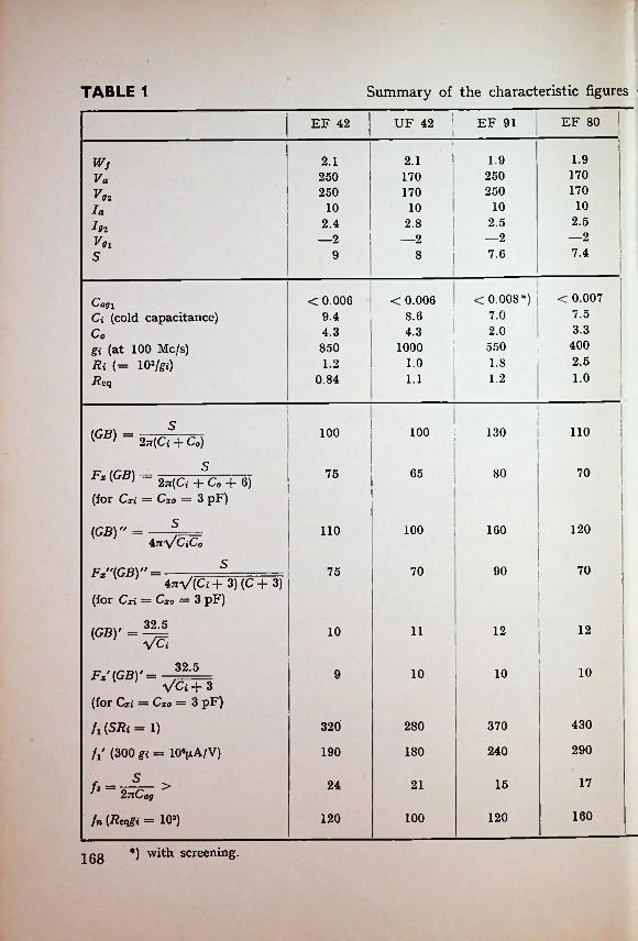
Summary of the characteristic figuresTABLE 1
EF 80UF 42 I EF 91EF 42
1.91.92.1 2.1Wf170250
250250 170Va
170250 170TV-101010 10la
2.52.52.4 2.8•V—2—2—2 —2TV7.47.6 !9 8S
< 0.008*) | <0.007< 0.006< 0.006Cag iC» (cold capacitance) 7.57.08.69.4
3.32.04.3 4.3Co400550850 1000gi (at 100 Mc/s)
Ri (= 10>/gi) 2.51.81.2 1.01.01.21.10.84Rcq
! Is no100 130100(G2?) =2jr(Ci -f- Co)
IS 7065 8075F* (GB) = II2yr(Ci -j- Co ~h 6)
(for Cxi = Cxo — 3 pF)■
5 120100 160110(GB)" =47t\/CiCo
5 7070 9075FX"(GB)" =4nV(Ci+3) (C+3)
(for Cxi = Cxo = 3 pF)
32.5 ! 121210 11(GB)' = vS;I32.5 1010109FX'(GBY =
VCi+ 3 (for Cxi — Cxo — 3 pF)
430320 280 370fi{SRi=l)
U (300 gi = 10VA/V)
5^ = >
fn (Rcqgi = 103)
290240190 180
17152124
160120100120
*) with screening.168
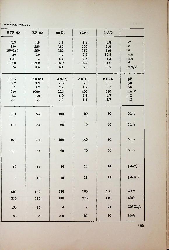
various valves
EFP 60 6AK5 6AU6EF 50 6CB6
Ii : ' w2.3 1.91.9 1.1 1.9 ;V250 250 i 180 200 250i :V150/250 250 150 150120mA9.5 10.820 10 7.7mA4.31.51 2.4 2.83V—2.0 —2.2 —1.0
. 5.2—2.0 —2.0
I mA/V6.225 6.5 5.1
pF0.00350.004 0.02 *) < 0.020< 0.007 ■
pF6.3 5.58.3 4.09.2pF1.9 55.2 2.86^A/V580125 460650 1000kQ1.78.0 2.21.5 1.0kfl1.6 2.71.91.45.7
IMc/s80120120260 75i
Mc/s507065190 55|■ I
!IMc/s80140120270 80
I jMc/s507065190 55
(Mc/s)1/.14131610 11
(Mc/s)1/*1111129 10
Mc/s
Mc/s
300350640620 250
240270510220 180)
104 Mc/s2474100 15 :
Mc/s8012020050 85
169
-
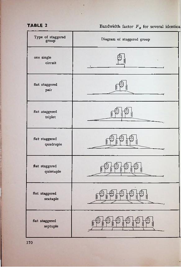
I
TABLE 2 Bandwidth factor FB for several identica
Type of staggered group Diagram of staggered group
one singlecircuit
i
flat staggered pair
i!flat staggered
triplet I
iii flat- staggered
quadruple;
!.!
flat staggeredquintuple
flat staggered sextuple
flat staggered septuple
170
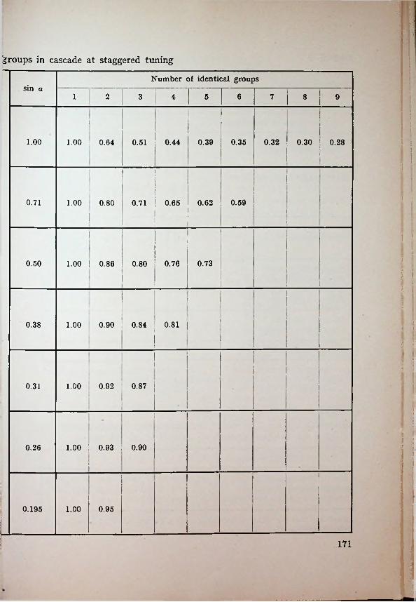
groups in cascade at staggered tuning
Number of identical groupssin a
1 2 63 4 5 7 8 9 Ii :
i • •1.00 0.39 0.35 0.32 0.30 1 0.281.00 0.64 0.51 0.44■ 'l .
I
'0.71 | 0.650.71 0.591.00 0.80 0.62
iII |
;1.00 0.86 0.80 0.730.60 0.76 |
! I
1'
t0.90 0.84 1 0.810.38 1.00 I •■
■
1.00 0.92 0.870.31 I
l
I
. i1.00 0.93 0.900.26
0.195 0.951.00
171
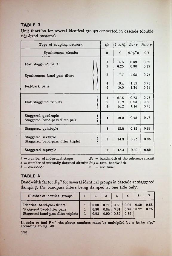
TABLE 3Unit function for several identical groups connected in cascade (double side-band systems).
t/s ! <$ in % I Br•Type of coupling network r B tot * t
Synchronous circuits 0.1/Fb0 0.7n
1 4.3 0.69 0.69Flat staggered pairs 2 6.25 0.90 0.72
3 1.05 0.757.7Synchronous band-pass filters
0.768.4 1.154Fed-back pairs 0.796 10.0 1.34
I8.15 | 0.73 0.7311.2 0.93 0.8014.2 1.14 0.78
1Flat staggered triplets 2
4
>Staggered quadruple Staggered band-pass filter pair 0.78 i 0.7810.91
1Staggered quintuple 0.82 ; 0.8212.81
Staggered sextupleStaggered band-pass filter triplet i ! 14.3 0.850.851
Staggered septuple 0.89 1 0.891 | 15.4
Br = bandwidth of the reference circuit1 = number of indentical stages 5 = number of mutually detuned circuits £tot= total bandwidth <5 = overshoot r = rise time
TABLE UBandwidth factor FB" for several identical groups in cascade at staggered damping, the bandpass filters being damped at one side only.
6 7Number of identical groups 51 2 3 4
0.59 0.56Identical band-pass filters Staggered band-filter pairs Staggered band-pass filter triplets
0.621 0.80 0.71 0.650.750.770.90 0.81 0.781 0.84
0.851 0.93 0.90 0.87
In order to find Fb", the above numbers must be multiplied by a factor Fni" according to fig. 48.
172
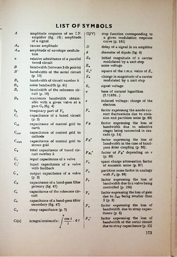
LIST OF SYMBOLSI C(/'*')A amplitude response of an I.F.
amplifier (fig. 19); amplitude of a signal
carrier amplitude amplitude of envelope modulation
relative admittance of a parallel tuned circuit
bandwidth (between 3 db points) bandwidth of the aerial circuit
(P- 10)bandwidth of circuit number h
step function corresponding to a given modulation response curve (p. 161)
delay of a signal in an amplifier diameter of dipole (fig. 6)initial magnitude of a carrier modulated by a unit step
noise voltagesquare of the r.m.s. value of Enchange in magnitude of a carrier modulated by a unit step
signal voltagebase of natural logarithm (2.71828...)
induced voltage; charge of the electron
factor expressing the anode current fluctuations due to emission and partition noise (p. 68)
factor expressing the loss of bandwidth due to selective stages being connected in cascade (p. 15)
factor expressing the loss of bandwidth in the case of bandpass filter coupling (p. 55).
factor of Fb" depending on r (P- 55)
space charge attenuation factor of emission noise (p. 67)
partition noise factor in analogy with Fk (p. 68)
factor expressing the loss of bandwidth due to a valve being controlled (p. 124)
factor expressing the loss of gain due to .Serf being smaller than 5 (p. 8)
factor expressing the loss of bandwidth due to stray capacitance (p. 8)
factor expressing the loss of bandwidth of the aerial circuit due to stray capacitance (p. 11)
A0 DA m d
Eba
EnBEn*B'Es
BhBn noise bandwidth (p. 61)
bandwidth of the reference circuit (p. 18)
maximum bandwidth obtainable with a given valve at a gain G0 (fig. 4)
imaginary part of Y0
EsBr e
B0 e
EaK ‘
Cc capacitance of a tuned circuit(P- 2)
FbC0 capacitance of control grid to earth
i
Ef/ik capacitance of control grid to cathode
capacitance of control grid to screen grid
total capacitance of tuned circuit number li
input capacitance of a valveinput capacitance of a valve with feedback
Fb"EgloZ
ChEn
C,Fk
C/
EPC. output capacitance of a valve(P- 2) FrCp capacitance of a band-pass filter primary (fig. 47)
capacitance of the reference circuit
:
Cr Ft
capacitance of a band-pass filter secondary (fig. 47)
stray capacitance (p. 7)
C8 ■
FxCx
XFxjSSLi.dtCi(,r) integral cosine of x:
o
173
List of Symbols
Fx" factor expressing the loss of bandwidth due to stray capacitance in the case of band-pass filter coupling (p. 54)
frequencycharacteristic frequencies in the linear approximations of a response curve (fig. 20)
gain reference frequency (fig. 3) gain reference frequency for the aerial circuit (p. 11)
frequency at which Lk is in resonance with Cglk
frequency at which Lk is in resonance with the cathode-to- earth capacitance
frequency at which Lk is in resonance with the cathode capacitor
frequency of the modulation noise reference frequency of a valve (p. 73)
stability reference frequency of a valve (p. 97)
self-neutralising frequency of a valve (fig. 89)
maximum frequency at which a given gain G0 can be obtained with a given valve (fig. 3); frequency of carrier
maximum frequency for the aerial circuit at which a given gain G0' can be obtained with a given valve (fig. 5)
(= VJVt) voltage gain (p. 1) gain of the aerial circuit (p. 10) voltage gain of stage number h maximum obtainable or permissible voltage gain
maximum gain obtainable with a given valve at a bandwidth B0 (fig. 3)
available power gain (p. 60) power gain at the frequency / power gain at the signal frequency
total voltage gain of an amplifier
(= G'y/W) gain bandwidth figure of an aerial circuit followed by a given valve (p. 11)
gain bandwidth figure of a valve (p. 54)
(= l/R) conductance or damping anode conductance of a valve, excluding l/ra (p. 2)
total conductance of a tuned circuit, excluding the valve damping
conductance of control grid to earth, excluding feedback damping and transit time damping
total damping of tuned circuit number h
input conductance of a valve input conductance of a valve with feedback
(= ga + l/ra) output conductance of a valve (p. 2)
conductance of the reference circuit (p. 18)
feedback damping in a valve real part of Y0transit time input damping of a valveelectric field strength unit step at the instant t step functionmagnitude of a component in linear approximations of a response curve (p. 32)
current or current variation anode current of a valve anode current fluctuation due to emission noise (p. 67)
control grid current screen grid current cathode currentcurrent fluctuation due to partition noise (p. 68) square root of minus one ratio of circuit damping to valve input damping
fraction of total input damping due to transit time effects
(GBy
[GBYfr.r s
Sa
fl!Sc
fl
folk' So 1:fk
Shfk
SiSi'f m
fnSo
fsSr
fsSt
fo s«s~
Hfo m
Hs(0h
GG' IGhGmax hGo Io
*02
IkG p I*(Gp)/(Gp), j
KiGtot(GB) gain bandwidth figure of a valve K 2
(P- 3)
174
List of Symbols
*3 P.i signal power at the input of an amplifiersignal power at the output of an amplifier
feedback parameter (pp. 87, 90) value of p2 for stage number h value of p2 for a stage the anode and grid circuits of which are identical to the reference circuit (p. 91)
quality factor of a tuned circuit (p. 134); in a bandpass filterQ = ^QpQs
quality factor of tuned circuit number li
Q of a band-pass filter primary Q of a band-pass filter secondary (= kQ) relative coupling coefficient of a band-pass filter
resistance
fraction of total noise due to partition noise (p. 69)
( = M/VLpLa) coupling coefficient of two coils; Boltzmann’s constant (= 1.37 X10⁻²³ J/OK)
inductanceinductance of an interstage circuit (p. 2)
inductance of the cathode leadinductance of a band-pass filter primary, including M
inductance of a band-pass filter secondary, including M
length of dipole (fig. 6)mutual inductance of a band
pass filter (fig. 47); modulation response of an I.F. amplifier (fig. 19)
real component of the modulation response (p. 34)
Mimag imaginary component of themodulation response (p. 35)
Mq reai real component of the modulation response for the quadrature component of the carrier (p. 40)
■Mq imag imaginary component of the modulation response for the quadrature component of the carrier (p. 40)
noise factor (p. 59) actual noise factor with a signal source of which Ts 5^ 288 °K
noise factor at correct matching noise factor with a signal source of which Ta = 288 °K
number of stages of an amplifier available power of a signal source
noise powernoise power at the input of an amplifiernoise power.at the output of an amplifiernoise power originating from a "noise resistance” (p. 62) signal power
P,ok
p°-PhT
L Pr2Lc
LkQLv
LsQh
lQvMQ*<1
R-^realanode load resistance of a valve, excluding Rc (p. 2)
feedback resistance between anode and grid
radiation resistance of an aerial
*«
Poo
R&n\.(P- 9)
parallel resistance of a tuned circuit (p. 2)
resistance equivalent to loading by a detector
grid leak resistance cathode resistance
Pc
Pj
PoNPkNa
load resistance of a diode detector (p. 13)
noise resistance (p. 63) total parallel resistance of a band-pass filter primary, including valve damping (fig. 47)
total secondary resistance of a band-pass filter secondary, including valve damping (fig. 47)
internal resistance of a signal source
input resistance of a valve due to feedback damping
(= l/gT) input resistance of a valve due to transit time damping
P<
NpractArst Pn
Pp
nP iPs
PnPni Ps
p x no Pt
Pnr
Ps
1751
!■
■
List of Symbols
( = QsfQp) ratio of the secondary to the primary quality factor of a band-pass filter (p. 53)
(= |J./S) internal resistance of a valve (p. 2)
mutual conductance of a valve (static value)(JlJJVg) anode transconductance
effective transconductance of a stage having feedback (p. 85); transconductance for the effective control voltage (p. 67)
mutual conductance of a valve (dynamic value)
{')Ik/ )Va) cathode transconductance
V0 output voltage e.m.f. in the aerial (p. 9) ratio of transformation of aerial circuit (fig. 6)
( = pQ = Aco/7tB) relative detuning expressed in half the bandwidth
value of x for circuit number h admittancevalue of y at the resonant frequency
admittance of circuit number h apparent value of Yh due to feedback effects
input admittance input admittance of a stage with feedback (p. 85)
output admittance output admittance of a stage
with feedback (p. 85) transfer admittance
Yh, h +1 transfer admittance of the interstage circuit between stages h and h + 1
admittance between anode and earth (fig. 72)
admittance between grid and earth (fig. 72)
admittance between anode and grid (fig. 72)
admittance between grid and cathode (fig. 72)
admittance between anode and cathode (fig. 72)
admittance between cathode and earth (fig. 72)
auxiliary quantity (p. 85) impedancevalue of Z at the resonant frequency
characteristic impedance of an aerial (p. 9)
grid circuit impedance of stage number ti
cathode impedance input impedance output impedance
rVraaw
raxS
SaYS'
V*Yk'Sett
YtSkY/
integral sine of x: j . d t YoSi(*)y '■* o
s(/r) step function corresponding to a given modulation response curve (p. 33)
maximum mutual conductance of a valve
number of staggered circuits in a flat staggered group (p. 17);
( = (S'0p) relative detuning of a trap with respect to the primary circuit expressed in half the bandwidth of the primary (p. 144)
absolute temperature; standard value 288 °K (p. 60)
noise temperature of signal source (p. 60)
time; number of tuned circuits in an amplifier
(= t + D) time corrected for delay in an amplifier
anode voltagevoltage between anode and control grid
output voltage of an aerial (p. 9) control grid voltage cathode voltage input voltage
Yt
S max
S
^3
Y4
TY&
TBYe
tY,ZV z
V a•ZantVv ag
ZhFant
vg ZkVk ZiVi Z0
176
List of Symbols
with respect to the reference circuit (fig. 8)
detuning of a signal with respect to the resonant frequency of a circuit (radn./sec)
overshoot of a step function (fig. 13); loss angle (p. 134)
detector efficiency delay angle (p. 31) wavelengthratio of circumference to diameter of circle (3.14159...)
auxiliary quantity (p. 85) rise time of a step function electron transit time from cathode to grid
angular frequency (radn./sec) resonant frequency of a tuned circuit (radn./sec)
impedance of the reference circuit of a staggering system
transfer impedance Z\, Zr,... inverse values of Yv Y„ . . .
(fig. 72)characteristic angle in staggering system (p. 18); ratio of noise temperature to standard temperature of 288 °K (p. 61)
value of a for circuit number hnoise temperature attributed to Rx (p. 70)
(= co/co0 — co0/<0 ^ 2Aco/co) relative detuning
value of (3 for circuit number hincrease of input capacitance due to space charge
detuning of circuit number h
Z t Aco
a
0 D0Xa h7C<*T
PT
~kg
■AC,- :CO
COq
A/, .;
i 11
;i
177
PHILIPS' TECHNICAL LIBRARY comprises 4 series of books:a. Electronic Valvesb. Light and Lightingc. Miscellaneousd. Popular series
The series a, b and c published in 6" x 9" are cloth bound, guilt. The dimensions of the popular series are 31" X bound in coloured "integral” binding.These books are mostly published in 4 languages: English, French, German and Dutch.
a. Series on ELECTRONIC VALVES:Book I Book II Book IIIBook IIIA "Data and Circuits of Receiver and Amplifier Valves”, 2nd Suppl.
by N. Markus and J. OtteBook IIIB "Data and Circuits of Receiver and Amplifier Valves”, 3rd Suppl.
by N. Markus"Data and Circuits of Television Valves” by J. Jager "Application of the Electronic Valve in Radio Receivers and Amplifiers”, Volume I, by B. G. Dammers, J. Haantjes, J. Otte and H. van Suchtelen Idem, Volume 2 Idem, Volume 3"Transmitting Valves” by P. J. Heyboer and P. Zijlstra
Book VIIIA "Television Receiver Design” 1, by A. G. W. Uitjens Book VIIIB "Television Receiver Design” 2, by P. A. Neeteson
Books IIIB, IIIC and VI are in preparation.
b. Series "LIGHT AND LIGHTING”1. "Physical Aspects of Colour” bij P. J. Bouma2. "Gas Discharge Lamps” by J. Funke and P. J. Oranje3. "Fluorescent Lighting” by Prof. C. Zwikker c.s.4. "Artificial Light and Architecture” by L. C. Kalff5. "Artificial Light and Photography” by G. D. Rieck and L. H. Verbeek6. "Manual for the Illuminating Engineer on Large-Size Perfect Diffusors”
by H. Zijl7. "Calculation and Measuring of Light” by H. A. E. Keitz
Books 4 and 7 exist in German only. An English edition of book 7 is in preparation
c. Series "MISCELLANEOUS”a. "Television” by Fr. Kerkhof and W. Wernerb. "Low Frequency Amplification” by N. A. J. Voorhoevec. "Metallurgy and Construction” by E. M. H. Lips
"Fundamentals of Radio-Valve Technique” by J. Deketh "Data and Circuits of Receiver and Amplifier Valves”"Data and Circuits of Reiceiver and Amplifier Valves”, 1st Suppl.
Book IIIC Book IV
Book V Book VI Book VII
;
d. "Strain Gauges” by Prof. J. J. Koche. "Introduction to the study of Mechanical Vibrations” by G. W. v. Santenf. "Data for X-Ray Analysis” I by W. Parrish and B. W. Inving. "Data for X-Ray Analysis” II by W. Parrish, M. G. Ekstein and B. W. Irwinh. "X-Rays in Dental Practice” by G. H. Hepple
Industrial Electronics” by R. Kretzmann
Books b, c, e, f, g and i are in preparation.
i.
POPULAR SERIES”The books of Philips’ Technical Library are on a rather high level. Again and again we received requests for technical books on a somewhat lower level. It was decided to comply with these requests and to bring such books in a "popular” series. Popular does not mean here superficial, but intelligible to a larger group of readers.
1. "Remote Control by Radio” by A. H. Bruinsma2. "Electronic Valves for L.F. Amplification” by E. Rodenhuis3. "The Odes and Trons Family” by J. Haantjes4. "Application of small Transmitting Valves for High Frequency and Trans
mission” by H. H. Mulder, D. Zaayer and P. J. Zijlstra5. "Photo Valves” by E. Rodenhuis.
Books 2, 3, 4 and o are in preparation.i
i
i
i