Embed Size (px)
Citation preview
~ . .. ' ....
TECHNICAL NOTE TN -1 i 19
COMPUTER, GUN DIRECTION Ml8 (F ADAC) APPLICATIONS MANUAL
by
THOMAS J. PRICE
Distribution of this document is unlimited.
MAY 1967
UNITED STATES ARMY FRANKFORD ARSENAL
PHILADELPHIA, PA.
Reproduced by lh~ CLEAR I N G HO USE
for Federal Scoonllfoc & T echnocal Informa tion Springfoold Va 22151
TECHNICAL NOTE TN-1119
COMPUTER, GUN DIRECTION M18 (F ADAC) APPLICATIONS MANUAL
by
Thomas J. Price
Distribution of this document is unlimited.
Fire Control Dev elopment and Engineering Laboratories FRANKFORD ARSENAL
Philadelphia , Pa. 19137
May 1967
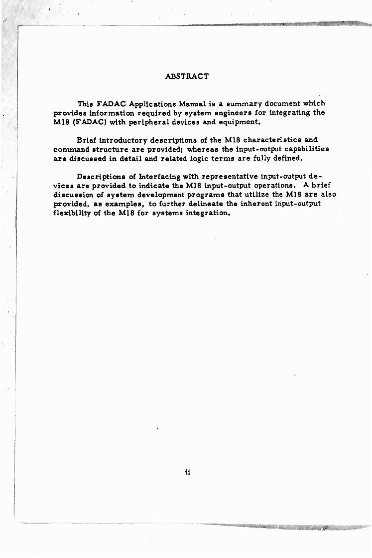
ABSTRACT
This FADAC Applications Manual is a summary document which provides information required by system engineers for integrating the M18 (FADAC) with peripheral devices and equipment.
Brief introductory descriptions of the M18 characteristics and command structure are provided; whereas the input-output capabilities are discussed in detail and related logic terms are fully defined.
Descriptions of Interfacing with representative input-output de- vices are provided to indicate the M18 input-output operations. A brief discussion of system development programs that utilize the MIS are also provided, as examples, to further delineate the inherent input-output flexibility of the MIS for systems integration.
ii
TABLE OF CONTENTS
Page
ABSTRACT
I. INTRODUCTION
A. General
B. Purpose and Scope
C. Manual Organization
II. COMPUTER CHARACTERISTICS
A. General
B. Functional Description
C. Command Structure
III. CONTROL PANEL
A. General
B. Functional Description
Operating Controls and Indicators . . . . ,
C. Control Panel Interfacing
1. Power Control 2. Set-Up Buttons 3. Keyboard 4. Mechanical Reader 5. Input Matrix 6. NIXIE Readout
2
2
5
18
35
35
37
37
41
41 41 44 44 50 53
iii
m
TABLE OF CONTENTS (Cont'd)
Page_
IV. EXTERNAL INPUT-OUTPUT INTERFACE DESCRIPTION 61
A. General 61
B. Detailed Input Description 63
1. Input Terms to GDC, MIS 63 2. Input Circuitry , 69
a. Input Datalines 69 b. Strobe 69 c. PS1 Pulse Stretcher 71 d. Neon Drivers 71 e. Discrete Input (F) Lines. ........ 77
C. Detailed Output Description 78
1. Output Terms 78 2. Output Circuitry 78
a. Output Datalines . . < 78 b. Strobe - Feedback 83 c. Remote Error Reset 85 d. Teletype Output 87 e. Amplifiers and Inverters 87
V. TYPICAL INPUT-OUTPUT DEVICES 88
A. Memory Loading Unit (MLU) 88
B. Digitronics Perforated Tape Reader 94
C. CTC Typewriter 99
D. Teletypewriter 101
E. LP-2-150 Paper Tape Punch 101
iv
TABLE OF CONTENTS (Cont'd)
Page
V. (Cont'd)
F. Magnetic Tape Bulk Memory 102
G. FADAC to FADAC 104
VI. SPECIALIZED APPLICATIONS 104
A. General 104
B. Automatic Calibration - Laboratory Evaluation Unit (Auto-Cal) 108
1. Buffer Translator 108 2. Computer Input Interface 110 3. Remote Program Addressing Ill
C. MAIDS MARK III Ill
1. Input-Output Buffer (IOB) 114 2. Computer Measurement Timing 118 3. External Device Integration 118
DOCUMENTATION LISTING 120
LIST OF ILLUSTRATIONS
Figure Title
1 Computer, Gun Direction Ml8 (FADAC) 3
2 Computer Block Diagram 6
3 Memory Contents 7
4 Computer Word Format . , , 8
•
LIST OF ILLUSTRATIONS (Cont'd)
Figure Title Page
5 Numeric Input Codes 12
6 Alpha-numeric Teletype Code 14
7 Alpha-numeric FIELDATA Code 15
8 Control Panel - Detail View 36
9 Control Panel Functions and Connector Assignments 37
10 PI Interface Schematic 42
11 "Operation" Switches, Computer Interface .... 43
12 P2 Interface Schematic 45
13 Keyboard Functional Diagram 46
14 Keyboard Timing Sequence 47
15 Mechanical Reader Functional Description .... 48
16 Mechanical Reader Timing Sequence 49
17 P5 Interface Schematic 51
18 Input Matrix Schematic 52
19 P6 Interface Schematic 54
20 NIXIE Display Block Diagram 55
21 NIXIE Anode Driver Schematic 56
22 NIXIE Cathode Driver Schematic 56
23 NIXIE Readout Schematic 57
24 NIXIE Display Arrangement 59
vi
LIST OF ILLUSTRATIONS (Cont'd)
Figure Title Page
25 Cathode Driver (CD) and Anode Driver (AD) Connections to NIXIE Display 60
26 Input Amplifier 61
27 Output Amplifier 62
28 Inverter 62
29 Schematic of Input Connector, J17 67
30 Input Line Timing 69
31 Inputting to FADAC 70
32 Steady State Strobe 72
33 Mechanical Contact Strobe 73
34 FIELDATA Strobe Timing 74
35 PS1, PS2 Pulse Stretcher 75
36 Neon Drivers 76
37 FADAC Bit Positions 78
38 Schematic of Output Connector, JIG 81
39 * FADAC Output Timing . 83
40 FADAC to Output Device Feedback 84
41 FIELDATA Strobe Feedback 85
42 Steady State Feedback 86
43 Switch Contact Feedback 86
vn
LIST OF ILLUSTRATIONS (Cont'd)
Figure Title page
44 Reset Button Interface 87
45 Teletype Output Waveform 88
46 Memory Loading Unit (MLU) 89
47 Memory Loading Unit (MLU) to FADAC Signals . . 90
48 MLU Timing 92
49 Oigitronics Tape Reader 95
50 FADAC to Digitronics Reader Cabling 96
51 Digitronic Tape Reader 97
52 SDR Simulator 98
53 Functional Diagram of FIELDATA Printer .... 100
54 "Mite" Teletypewriter 102
55 Tape Tub 103
56 FADAC - Tape Tube Interface 105
57 FADAC to FADAC, FADAC Strobe 106
58 FADAC to FADAC, FIELDATA Strobe 107
59 Auto-Gal Systems Concept 109
60 Remote Program Addressing 112
61 Auto-Gal Information and Control Lines 113
62 MAIDS MARK III 115
63 IOB Block Diagram 116
vm
I. INTRODUCTION
A. General
The Computer, Gun Direction M18 (Field Artillery Digital Auto- matic Computer, FADAC) is a general purpose transistorized digital computer designed for field use. The M18 (FADAC) was designed pri- marily to compute firing data for artillery weapons from data inputs defining target location, weapon location, and prevailing conditions of equipment, material, and weather. The control panel has been human engineered for efficient and easily learned operator control. The mark« ings on the control panel are those associated with the artillery weapon problem but with little or no change can be readily adapted to a wide range of applications. An input-output interface is also provided which permits the computer to comrr. nicate with or control many types of devices.
The primary design requirements make it ideally suited for many real time applications.
B. Purpose and Scope
The purpose of this manual is to present the technical information required by the System's Engineer for application of the FADAC, as well as the interface and function data to permit the most efficient integration of the computer into a contemplated system configuration.
The primary characteristics of the computer are listed and a brief explanation of the computer instructions is also provided. For a complete description of the programming aspects of the computer, the programming manual, FCDD-361, Volume IV, Revision I, is avail- able.
C. Manual Organization
This manual contains six major sections. The first section is an introduction to the M18 (FADAC) computer and also explains the purpose of this manual. Section II is directed to the MIS computer characteris- tics including command structure and computer operations. Section III
s
describes the Control Panel and detailed interfacing of the Control Panel to the main frame. Section IV is a detailed input-output inter- face description of the M18 computer. Section V contains a brief de- scription of some presently used devices providing input-output with the M18 computer. Section VI describes the M18 as it is systems con- figured and indicates the related input-output characteristics.
II. COMPUTER CHARACTERISTICS
A. General
The Computer, Gun Direction, MIS (FADAC) is shown in figure I. Major controls and location of external connectors are shown. A brief summary of general computer characteristics is presented below:
GENERAL CHARACTERISTICS
Size: 24 inches by 14 inches by 34 inches
Weight: Approximately 210 pounds
Power: Three-phase, 4-wire, 400 hz system; 120/208 volts, approximately 750 watts
Temperature: -25* F to 125° F (external ambient at sea level); with rear cover installed, to -40* F. Auto- matic temperature protection is provided.
Commands: One command per word; each command con- tains both address of operant and address of next command.
Numbers: Straight binary for internal operations; automa- tic conversion to other codes for input-output; two's complement notation for negative numbers.
«
u <
00
§
a
i
Word Length: Thirty-two binary digits; sign bit and 31 binary digits for absolute numerical value.
Memory Type: Magnetic Disc, 6000 rpm nominal speed of rotation. Automatic frequency and voltage protec- tion is provided.
Storage Capacity: Sixty-four channels of 128 words each (8192 words) in main memory. Also provided are two 16-word high-speed loops for rapid access, five 1-word registers for arithmetic operations and con- trol, and one 2-word register for output display- information storage. All channels and loops have one read and one write head except the 16-word loops which have an additional read head.
Pulse Repetition Rate: Nominal pulse repetition rate, 460 kilopuls es per second.
Internal Information Flow: Serial by bit, parallel by function, allowing 12,800 one-word execute (add, subtract, etc.) operations per second. Multiplication and di- vision require 18-word execute cycles.
Input: Inputs to the computer are from the manual keyboard or the mechanical tape reader on the control panel. External sources may load the computer. Typically:
1. Mechanical keyboard or mechanical reader to 30 cps.
2. Numeric devices to 600 cps,
3. Alphanumeric devices to 4000 cps.
Inputs may use 5-channel code for teletype operation or 8-channel code for FIELDATA operation.
Output: Primary output is to the visual display (NIXIE). Signals are provided for operating external printers, magnetic tape units, and other FIELDATA or tele- type equipment. Output information is in 5-level
teletype, 2-wire teletype, or FIELDATA codes as required. Output rate is approximately 4000 for alphanumeric and 600 for numeric.
Additional Features of the Computer:
Parity check on information transfers. Verify indicator (located on tape reader) on input in program fill mode. Gating for external support equipment to permit logic failure isolation to single printed circuit board. Marginal test circuit for preventive maintenance. Voltage transient warning indicators. Temperature warning indicators. High speed (2 bits-at-a-time) multiplication, divi- sion, and shifts. Self-checking for overflow. Standardized printed circuit boards to minimize logistic problems.
B, Functional Description
1, General
A block diagram of the logical organization of the computer is shown in figure 2, The largest single part of the computer is the control and arithmetic logic which through means of the control panel and/or external input devices establishes various modes of reading instruction or information words from memory, performing all the various instructions listed in Section II, C, writing into memory and communicating with the control panel and external devices,
2. Summary of Functional Characteristics
2, 1 Computer Word Formats and Storage Capacity - Infor- mation stored in memory contains no inherent distinction between numerical data and computer instructions. Memory outputs are inter- preted in accordance with the state of computer logic elements classi- fied as mode controls. Various word formats have been developed to relieve the operator of as many time-consuming number conversions as possible.
J12, J13, J14, J15, J16
Access for Testing
J17 Input . Interlace to external devices
MEMORY
READ-WRITE CIRCUITRY
HI CONTROL AND ARITHMETIC
LOGIC
in I/O
CIRCUITRY
I CONTROL
PANEL
I/O J10 CIR- Output CUITRY interface
to external devices
Figure 2. Computer Block Diagram
2. 1. 1 Memory Capacity - Information is stored in the com- puter memory in binary code - 32 bits per information word. In addi- tion, 3 bits are used for synchronization and one bit for parity informa- tion, giving a total of 36 bits per machine word. The capacity of the memory is given in figure 3, including the storage capacity of registers normally required to perform program functions.
REGISTER
R
Q
A
L
N
Do» DI
Main Memory
I
X
CAPACITY
16 words S
16 words
1 word
1 word
1 word
2 words
8192 words ^
1 word "1
1 word J
may be stored into
by program
may not be stored
into by program
Figure 3. Memory Contents
2. 1. 2 Number Formats - In addition to the normal binary representation of numbers, other number formats are available for use by external devices.
2. 1. 2. 1 Binary Representation - Information used by the computer as an operand is interpreted as a signed, 31-bit, binary coded word with a fixed binary point located between the sign bit and most sig- nificant digit. Positive numbers have a zero sign bit and negative num- bers a one sign bit. Negative numbers are stored and interpreted in two's complement form. Binary representation is shown in figure 4(b) that indicates 31 bits allocated for the numerical value and the 32nd bit for the sign designation.
s H
§
s
i ON
[SI
f)
SO
gwHoa M
oo
CSJ
■§■ CM
a
1
}
S I El J a .a
ii-( 1^ "1 1 tM
pT [^ in
IvO r / u r* i 00
£ as
rer TJ Ng M
| gj 1 3 M
u | r-i 3
La. «n
u iffi -y i^ H 0
% 9 ON S " T «H
■e- h N
CM CM
-SL •>t MJ -^ S s y)| S i V,
SJ w
i! CMJ
< 1
o o\\ H f
en »51
^,. „ <^ g " " V. z ' n
| eN4 SS 1 -aJ ^ „ ,.-.^
§
2. 1. 2, 2 Octal Number Representation - Each group of three binary digits, beginning with the three least significant digits of the word, are interpreted as a number to the base eight. The sign and most significant digit are grouped together and interpreted as a number to the base four. Octal representation is shown in figure 4(b).
2. 1. 2. 3 Alpha-numeric Representation - Certain input and output operations require recognition of mixed alphabetic and numeric symbols. Alpha-numeric information requires sufficient bits for non- ambigous representation of each symbol (figure 4(c)).
2. 2 Instruction Word Format
2.2. 1 Instruction Words - Computer words containing pro- gram information are interpreted by the computer as instructions when properly sequenced. If required by the program, certain portions of in- struction words may be treated as operands. Instruction words contain an operation code, an operand address, and the address of the next se- quential instruction. Instruction word composition is shown in figure 4 (a).
2,2.2 Octal Instruction Representation - Information con- tained in an instruction word may be interpreted as a sequence of num- bers to the base eight as defined above. Octal instruction representa- tion is shown in figure 4(a).
2. 2. 3 Quasi-Octal Representation - In the instruction word the octal digits overlap logical portions of the word; which makes it in- convenient to write an instruction word in true octal form. For this reason, instructions are usually written in quasi-octal form. Octal digits that overlap instruction word subunits are split into two quasi- octal digits. After the program is written, adjacent quasi-octal digits are summed for the final form of the program. Quasi-octal represen- tation is shown in figure 4 (a).
2, 3 Memory Disk - The memory disk consists of functional bands, or channels each with read and write heads.
2. 3, 1 Sector Track - The Sector track is permanently re- corded, and has external connections only to the read head. Its purpose is to notify the control unit which sector is about to pass under the read heads of the other channels. The main memory read heads are all at the same effective sector location.
2. 3. 2 Main Memory - There are 64 main memory channels and are numbered evenly from 000 through ISbg and 30Ug through 3363. Words or sectors of each channel are numbered in consecutive octal numbers from 000 to 177 inclusive,
2. 3. 3 Short Loops - A, L, N, D, R, and Q are short re- circling loops. Each bit is sensed by the read head and rewritten by the write head. Each word is shifted, bit-by-bit, through the loop. The loop information remains the same unless changed by some arith- metic or control operation. A, L, and N are 1-word loops whose con- tents are rewritten each word time. O is a 2-word loop, and R and Q are 16-word storage loops. Rand Q each have a secondary read head located in the middle of the loop. This head is not involved in the re- circulation process.
2,3.4 Short Loop Addressing - The rapid access loops R and Q may have sector address 000 to 177, but only the last four bits are recognized. The channel address of R is 142; Q is 152. Registers A, L, and N are all addressable. The program may store into and read out of them or they may be used as temporary storage for operands and instructions when not required by the program operations. The sector number has no significance when addressing A, L, or N. because they are one word loops. The display register is a 2-word loop in channel 160, The right word is addressed by odd sector numbers and even sec- tor numbers refer to the left word; where the relative position of each word is defined with respect to the Control Panel display.
2.4 Input
2.4. 1 Initial Program Fill - The normal form of input for loading a program into memory, is the octal mode. Information is, loaded in octal Teletype or FIELDATA code. The basic form of the program is as follows:
a. The memory location of incoming words is specified with five octal characters (channel and sector) followed by a "LOCATION" code. The channel and sector are read into A. The "LOCATION" code transfers these bits to the L register. A new location may be specified at any point in the program.
b. The program and constants are entered in octal digits; 11. characters per word; and each word followed by an "ENTER" code. The "ENTER" code stores the contents of A in the location
10
contained in L, and then increases L by one. In this way, incoming words are stored in sequential location, unless a new location is en- tered.
c. During octal fill, control is dependent upon the input lines and not the computer itself. If it is desired to proceed directly from input to computing, the last characters should be five characters specifying the start address, followed by a "LOCATION" code and a "COMPUTE" code. The five characters load into A; the "LOCATION" code transfers A to L; then the "COMPUTE" code begins computation at the address specified in L when the computer is put in the "RUN" mode.
2. 4, 2 Computer Initiated Inputs
2.4.2. 1 Octal Fill - Using the input commands, the com- puter will:
a. Accept FIELDATA or Teletype characters as listed in figure 5.
b. Convert FIELDATA and Teletype codes listed in figure 5, and additionally the blank tape code, to a four-bit code. This conversion is accomplished by the code conversion information written on the Sector channel.
c. Interpret the four-bit code derived from b as one of the following:
1. An octal character, and insert it into the A register.
2. A "FILL" code, and initiate "FILL" mode.
3. A "VERIFY" code, and initiate "VERIFY" mode.
4. A "LOCATION" and transfer the contents of A to the L register.
5. An "ENTER" code, and will transfer the contents of A to memory if in the "FILL" mode or will compare the contents of A to memory if in the "VERIFY" mode.
11
^
"T-r- ■
•
j Teletype Meaning FADAC Meaning Fieldata Meaning
Character Tape Code
Octal j Mode
BCD | Mode
Binary Conversion
Tape Code Character
0, P 01101 0 0 0000 00110000 0
I. Q \ 11101 1 1 0001 10110001 1 1 2, W 11001 2 2 0010 10110010 2 1
3, E 10000 3 3 0011 00110011 3
4, R 01010 4 4 0100 10110100 4
5, T 00001 5 5 0101 00110101 5
6, Y 10101 6 6 0110 00110110 6
7. U 11100 7 7 0111 10110111 7 1
8, I i
01100 Halt 8 1000 10111000 8
9. 0 00011 Compute 9 1001 00111001 9
(+) n. z 10001 Fill + 1010 00100010 +
I -. A 11000 Verify | - 1011 IOOlüOOOl . l
i •• M 00111 Location • 1100 10111101 j • i;
/. x 10111 Clear Cleai 1101 11011101 | X |
Car. Ret 00010 Enter Entei 1110 01000100 Car. Ret
Blank 00000 Blank Blanl : 1111 00000000 Blank
NOTE: The above codes are employed in numeric input-output in the BCD and octal modes.
Figure 5. Numeric Input Codes
12
6. A "HALT" code, and will go to the "MANUAL HALT" mode.
7. A "COMPUTE" code, and will initiate the "COMPUTE" mode if the computer is in the "PROGRAM HALT" mode.
2. 4. 2. Z Decimal Fill - Using the input commands, the computer will:
a. Accept and convert up to 16 binary-coded decimal characters, and will store them by character in A and N on input.
b. While in "DECIMAL FILL BY WORD", convert and store 8 characters per work in A and store the contents of A in memory after each 8 characters.
2.4.2. 3 Alpha-numeric Fill - Using the input commands and the codes listed in figures 6 and 7 for "Alpha-numeric-5" and "Alpha-numeric-6", the computer will:
a. Accept up to 10 characters and will store them by character in A and N while in "Alpha-numeric-5 Fill" by character.
b. Store 5 characters per word in A and store the con- tents of A in memory after each 5 characters while in " Alpha - nume ric- 5 Fill" by word.
c. Accept up to 12 characters and will store them by character in A and N while in "Alpha-numeric-6 Fill" by character.
d. Store 6 characters per word in A and store the con- tents of A in memory by word, after each 6 characters while in "Alpha- numeric-6 Fill By Word".
2.5 Output
2. 5. 1 NIXIE Display - The NIXIE tubes on the Control Panel are activated by the command "INITIATE DISPLAY". The con- tents of DQ and Dj are displayed as binary-coded decimal numbers. In order to display binary numbers, the program must convert them to decimal, store the eight most significant decimal digits in D^ , and
13
m •
TELETYPE CHARACTER TELETYPE CODE
0, P 01.101 1, Q 11.101 2, W 11.001 3, E 10.000 4, R 01.010 5, T 00.001 6, Y 10.001 7, U • 11.100 8, I 01.100 9, 0 00.011 + , Z 10.001
, A 11.000 ., M 00.111 CARR. RETURN 00.010 /, X 10.111 ), L 01.001 :, C 01.110 • , N 00.110 1, F 10.110 s, S 10.100 H, H 00.101 $, D 10.010 &, G 01.011 (, K ll.UO FIGURE SHIFT 11.011 ;. v 01.111
10.011 LETTERS SHIFT 11.111 LINE FEED 01.000 SPACE 00.100 BLANK 00.000 ., J ii.oio
Figure 6. Alpha-numeric Teletype Code
14
FIELDATA u
1 FADAC FIELDATA
u
1 FADAC
1 Tape Code Upper Case Binary Code
2 Tape Code Upper Case Binary Code
PC11DDDD i-J PC11DDDD
11000000 Master Sp * 000000 10100000 ) 100000 01000001 Upper case \ 000001 00100001 - 100001 01000010 Lower case X 000010 00100010 + 100010 11000011 Tab o 000011 10100011 < 100011 01000100 Car. ret < 000100 00100100 ■ 100100 11000101 Space A 000101 10100101 > 100101 11000110 A A 000110 10100110 100110 01000111 B B 000111 00100111 $ 100111 01001000 C C 001000 00101000 * 101000 11001001 D D 001001 10101001 ( 101001 11001010 E E 001010 10101010 II 101010 01001011 F F 001011 00101011 : 101011 11001100 G G 001100 10101100 ? 101100 01001101 H H 001101 00101101 • 101101 01001110 I I 001110 00101110 • 101110 11001111 J J 001111 10101111 Stop© 101111 01010000 K K 010000 00110000 0 110000 11010001 L L 010001 10110001 1 110001 11010010 M M 010010 10110010 2 110010 01010011 N N 010011 00110011 3 110011 11010100 0 0 010100 10110100 4 11U100 01010101 P P 010101 00110101 5 110101 01010110 Q Q 010110 00110110 6 110110 11010111 R R 010111 10110111 7 110111 11011000 S S 011000 10111000 8 111000 01011001 T T 011001 00111001 9 111001 01011010 U U 011010 00111010 i 111010 11011011 V V 011011 10111011 t 111011 01011100 W w 011100 00111100 1 111100 11011101 X X 011101 10111101 • 111101 11011110 Y Y 011110 10111110 Special a 111110 01011111 Z Z 0111111 00111111 Back space 111111
87654321 87654321
NOTE: Paper tape Fieldata codes are shown. Magnetic Tape Fieldata codes can be obtained by inverting parity bit (8) in column 1 and control bit (7) in column 2.
Figure 7. Alpha-numeric FIELDATA Code
15
■
the seven least significant decimal digits in DQ . The sign must be ex- amined, and + or - code (four bits) stored in the four least significant bits of DQ .
Once the "DISPLAY" mode is entered it will continue until the order is given to "HALT DISPLAY". Computation may pro- ceed during display.
2. 5,2 Octal Output - Using the Octal output commands the computer will:
a. Convert the octal characters in A and N to their FIELDATA or Teletype equivalent via the Sector track conversion table, and generate a carriage return after every eleventh character while in "OCTAL OUTPUT BY CHARACTER".
b. Continually load A and N with the words from main memory to be transmitted and proceed as per "OCTAL OUTPUT BY CHARACTER" while "OCTAL OUTPUT BY WORD".
2. 5, 3 Decimal Output - Using the output commands the computer will:
a. Convert the decimal characters in A and N to their FIELDATA or Teletype equivalents via the Sector track conversion table, while in "DECIMAL OUTPUT BY WORD".
b. Continually load A and N with the words from main memory to be transmitted and proceed as per "DECIMAL OUTPUT BY CHARACTER", while in "DECIMAL OUTPUT BY WORD".
2. 5. 3. 1 Alpha-numeric Output - Using the output commands the computer will:
I a. Send up to four 8-bit characters from A while in
"ALPHA-NUMERIC-4 OUTPUT". In "ALPHA-NUMERIC-4 OUTPUT" the output lineDSOO will be the inverse of the appropriate bit stored in the computer word being outputted.
b. Continually load A and N with the words from main memory to be transmitted, and send 5 characters per word while in "ALPHA-NUMERIC-5 OUTPUT BY WORD".
16
I ■
c. Send 6 characters per word from A and N while in "ALPHA-NUMERIC-6 OUTPUT BY CHARACTER".
d. Continually load A and N with the words in main memory to be transmitted and proceed as per "ALPHA-NUMERIC-6 OUTPUT BY CHARACTER" while in "ALPHA.NUMERIC-6 OUTPUT BY WORD".
2.5.3.2 Two-wire Teletype Output - The Teletype oscilla- tor provides a precision time reference for computer 2-wire, 5-level (serial) Teletype output. Machine logic is such that a character of in- formation may be transmitted if that information already exists in an applicable register of the computer in teletype code.
2. 5. 3. 2. 1 Format - A start pulse is defined as minus 3 volts and a stop pulse as 0 volts. A start pulse of 1 unit time precedes information pulses. The start pulse is followed by 5 units of informa- tion, and terminated by a stop pulse. The stop pulse must be at least 1.42 units. A unit of time is defined as 22 milliseconds ± 5 percent. The stop pulse cannot be less than 1.42 units; and, since a unit cannot be divided, two units of time are used as the stop pulse (44 milliseconds).
2. 5. 3. 2. 2 Operation - The output signal from the Teletype oscillator is called the F32 line (or term). F32 is referred to as the sampling line. Sampling occurs by the X-special command "READ SWITCH MATRIX". The X-special command causes the 32nd bit in the A-register to become one or zero, depending on the state of the sampling line. Upon a command such as "TRANSFER ON POSITIVE", if the F32 line has b^en setting true for 11 milliseconds, the A-register has been receiving a one in the sign position (32nd bit) indicating a nega- tive number. Assume next that F32 goes false and a zero replaces the one in the sign bit of the word. With the advent of the zero, the "TRANS- FER ON POSITIVE" command causes the output driver to transmit a true signal (-3 volts), which is the start pulse. During output of the start pulse, F32 again goes true. A delay occurs until the F32 line again goes false, at which time the second bit of the character is sent out. The process continues through the remaining bits of the charac- ter, after which the stop pulse is sent out, permitting a new character to be transmitted.
2.6 Input-Output Terms - The terms associated with the input-output connectors are described in detail in a subsequent section, Section IV, B, of this manual,
17
.
C. Command Structure
For a complete description of the programming aspects of the computer, refer to FCDD-361, Volume IV, Aevision 1, Gun Direction Computer XM18 (FADAC) Programming Manual.
A brief explanation and summary of computer operations is pre- sented below:
Operation Commands
HALT, HLT: Execution word times; Execution:
36, C = 120 1 Computation is halted. Flag bit and operand address are ignored by this command.
INITIATE DISPLAY MODE, IDM: Execution word times; Execution:
36, C - 164 1 Visual display activated until a HALT DISPLAY command Is received. Sixteen binary-coded decimal (BCD) digits at a time are displayed from the 2-word D register. Computations can proceed while In this display mode. Flag bit and operand address are ignored by this command.
HALT DISPLAY MODE, HDM: Execution word times; Execution:
36, C - 166 1 Visual display mode halted. Flag bit and operand address are ignored.
HALT COMPUr^", LIGHT HCL: Execution word times: Execution:
36, C » 124 1 The compute light will be turned off with the computation mode unaffected.
18
■ .
INITIATE COMPUTE LIGHT ICL: Execution word times: Execution:
36, C - 126 1 The compute light will be turned on. Compi'tation mode will be unaffected.
DISCRETE INPUT TO ACCUMULATOR, DIA: Execution word times: Execution:
A Register Bits
1
2 - 7 8 9 - 13
14 - 30 32
DISCRETE OUTPUT: DO 0 DO 1 DO 2 DO 3
Execution word times: Execution:
36, C = 040 1 Information on 32 discrete input lines are input Into the A register, enabling program to sample various input signals in A register. Currently these are as follows: (flag bit and operand address are Ignored).
Contents
Signal that both column and row matrix buttons have been depressed Matrix Code Control Panel button 1 or 2 depressed Control Panel button A, B, C, D, or E depressed Spare bits for external inputs Two-wire Teletype timing signal for programming
36, C 36, C 36, C 36, C
1 The eight DO commands can set a 3-bit register to any one of Its eight possible counts. This register, in turn, controls several output lines and lights. Currently, the eight counts are used as follows:
100 DO 4 36, C - 110 102 DO 5 - 36, C - 112 104 DO 6 - 36, C - 114 106 DO 7 36, C - 116
19
• ■
Control Conmands
TABLE SEARCH EQUALITY, EQS: Execution word times: Executions:
Count To Function
OPLO Idle 0PL1 Output plug OPL2 Output plug OPL3 Output plug 0PL4 Input plug 0PL5 Input plug 0PL6 Input plug OPL7 No Solut
64 2 minimum Starting with 1=0, the contents of the A register are compared with those In memory location (m + 1) In bit positions as Indicated by a mask appearing in the L register. This mask must have been stored in the L register by the program. It directs which bits of the A register and memory should be compared. Whenever a 1 appears in the L register, the corresponding bits in A and (m + 1) will be checked. If in the designated bit positions the contents of the A reglstex are found to be equal to the contents of (m + 1), the ensuing word in memory (m + 1 + 1) is put into the A register. At this time, if the flag bit of the command is a 1, the contents of the A register will be transferred to the L register. If the flag bit is a 0, the contents of the L register remain unaltered. If the contents of the A register, in the designated bit positions are not equal to the contents of (m + i>, then 1 is increased by one and the comparison continues if the end of a channel has not been reached. If the end of the channel has been reached, the operation is terminated.
20
GREATER THAN OR EQUAL SEARCH, GES: Execution word times; Execution:
66 2 minimum Starting with i = 0, the contents of the A register and memory location (m + i) are compared in bit positions as directed by a mask appearing in the L register. This mask must have been stored in the L register by the program. It informs the computer of the bits of the A register and (m + 1) that should be compared. Whenever a 1 appears in the L register, the corresponding bits in A and (m + i) will be checked. If in the designated bit positions (m + 1) (A), then the ensuing word (m +1 + 1) is put into the A register. At this time if the flag bit of the command is a 1, the contents of the A register are transferred to the L register. If the flag bit Is 0, the contents of the L register remain unaltered. If in the designated bit positions the contents of the A register are not less than or equal to the contents of (m + 1), then 1 is increased by one and the comparison continues if the end of the channel has not been reached. If the end of the channel has been reached, the operation Is terminated.
Arithmetic Commands
ADD, ADD m: Execution word times: Execution:
00 1 The word in location m Is added to the contents of the A register and the sum is stored in the A register. Overflow can occur and, unless followed by a TRANSFER ON OVERFLOW command, the com- puter will halt with an error indication. A flag bit of 1 will cause the contents of location m to be put into the N register. A flag bit of 0 leaves the contents of the N register unaltered.
21
SUBTRACT, SUB m: Execution word times; Execution:
MULTIPLY, MPY m: Execution word times: Execution:
02 1 The word location m is subtracted from the A register, the difference appearing in the A register. Overflow can occur and, unless followed by a TRANSFER ON OVERFLOW command, will cause the com- puter to halt and indicate an error. A flag bit of 0 leaves contents of N register unaltered.
20 18 The contents of memory location m are multiplied by the contents of the A register. The product appears in the A and L registers unrounded. The most significant 31 bits and sign are in the A register. The least significant 31 bits are in the L register. Because the number in the L register is the least significant part of the total product, it does not have a sign asso- ciated with it. The most significant bit of the 31 bits of the least sig- nificant part of the product appears in the sign position of the L register. The least significant bit position of the L register always contains a 0 after multiplication which is not considered a part of the product. The contents of location m are storöd in the N register. The flag bit is ignored by this instruction.
DIVIDE, DIV m: Execution word times: Execution:
22
30 18 The 62-bit number appearing in the A and L registers is divided by the con- tents of location m. The most signi- ficant bit of the portion of the dividend that appears in the L register is in the sign position. If the flag bit is 0, then the A register will contain the rounded quotient and the L register will contain the unrounded quotient and the L register will contain a remainder with the same sign as the divisor. This re- mainder satisfies the relation: Divisor x Quotient + Remainder = Dividend. The contents of location m are put in the N register.
• '
Overflow can occur if the absolute value of the contents of the A register is equal to or exceeds the absolute value of the contents of m. In case of over- flow, the computer will halt with an error signal unless the command is followed by a TRANSFER ON OVERFLOW command.
Semiarithmetic Commands ACCUMULATOR RIGHT CYCLE, ARC S: Execution word times: Execution:
ACCUMULATOR RIGHT SHIFT, ARS S: Execution word times: Execution:
76, C - 00 1/2 (1 + S + cos 27TS/2) The sector address portion of this com- mand does not refer to a location in memory, but indicates the number of binary positions the word in the A register is to be cycled. On execution of this command, the contents of the A register are shifted right the number of binary positions designated by S. The bits shifted off the right end of the A register appear at the left end of the register in the same sequence being shifted in through the sign bit. The flag bit must be a 0.
76, C » 02 1/2 (1 + S + cos 27)5/2) The sector address portion of this command does not refer to a location in memory, but indicates the number of binary positions the word in the A register is to be shifted. On execution of this command, the contents of the A register are shifted right the number of binary places designated by S. The sign is spread in the left-hand bits, while bits shifted beyond the right-hand limits of the A register are lost. The flag bit must be a 0.
ACCUMULATOR LEFT CYCLE, ALC S: Execution word times: Execution:
76, C = 04 1/2 (1 + S + cos ZvS/Z) The sector address portion of this command does not refer to a location in memory, but indicates the number of binary positions the word in the A re- gister is to be cycled. On execution of this command, the contents of the A register are shifted left, through the sign bit, the number of binary places
23
ACCUMULATOR LEFT SHIFT, ALS S: Execution word times: Execution:
indicated by S. The bits shifted off the left end of the register are shifted in at the right end in the same sequence. The flag bit of 1 indicates that the computer should check for overflow.
76, C - 06 1/2 (1 + S + cos 2ffS/2) The sector address portion of this command does not refer to a location memory, but indicates the number of binary positions the word in the A register is to be shifted. On execution of this command, the contents of the A register are shifted left, through the sign bit, the number of binary places designated by S. Positions left vacant, as the contents in the A register are shifted left, are filled with zeros. Any bits shifted beyond the sign position of the A register are lost. It is possible to have an overflow with this command.
LONG RIGHT CYCLE LRC S: Execution word times: Execution:
A flag bit of 1 indicates that the computer should check for overflow. When the flag bit is 0, overflow is ignored.
76, C = 20 1/2 (1 + S + cos 2TrS/2) The sector address portion of this command designates the number of binary places the information is to be cycled. Upon execution of this command, the contents of the A and L registers are shifted off the right end of the A register through its sign bit position. The bits shifted off the right end of the L register are shifted into the A register through its sign bit position. The flag bit must be 0.
24
■ .
LONG RIGHT SHIFT, IRS S: Execution word times: Execution:
76, C = 22 1/2 (1 + S + cos 2^5/2) The sector address portion of this command designates the number of binary places the information is to be shifted. Upon execution of this command, the contents of both the A and L registers are shitted right the number of binary places designated by S. The bits shifted off the right end of the A register are shifted into the L register through its sign bit position. The bits shifted off the right end of the L register are lost. The sign of the A register is spread. The flag bit must be a 0.
LONG LEFT CYCLE, LLC, S: Execution word times: Execution:
LONG LEFT SHIFT, LLS S: Execution word times: Execution:
76, C = 24 1/2 (1 + S + cos 21TS/2) The sector address portion of this command designates the number of binary places the information is to be cycled. Upon execution of this command, the contents of the A and L registers are shifted left the number of binary places indicated by S. The bits shifted left through the sign of the A register are shifted into the right end of the L register. Bits shifted through the sign bit of the L register are shifted into the right end of the A register. The flag bit is ignored for this command.
76, C = 26 1/2 (1 + S + cos 2TrS/2) The sector address portion of this command designates the number of binary places the information is to be shifted. Upon execution of this command, the contents of both the A and L registers are shifted left the number of binary places designated by S. The bits shifted through the sign bit of the L register are shifted into the right-hand end of the A register. The right-hand bits of the L register vacated by the shifting process are filling with zeros. Bits shifted off the left-hand end of the A register are lost. It is possible to have overflow with this command. A flag bit of 1 indicates the computer should check for overflow.
25
.
Control Transfer
TRANSFER ON PLUS, TPL: Execution word times: Execution:
TRANSFER ON OVER- i'LOW, TOV m: Execution word times: Execution:
10 1 Control is transferred to the instruction found in location m if the contents of the A register are greater than or equal to zero. If the contents of the A regis- ter are negative, the address of the next instruction to be executed is obtained from the NEXT INSTRUCTION address of the command. If the transfer is executed, a flag bit of 1 will put the instruction into the N register. A flag bit of 0 leaves the contents of the N register unaltered.
16 1 Control is transferred to the instruction found in location m when an overflow has occurred as a result of the previous in- struction. If no overflow has occurred, control will proceed to the next instruc- tion. If the transfer is executed, a flag bi«- of 1 will put the instruction into the N register. A flag bit of 0 leaves the N register unaltered.
TRANSFER UNCON- DITIONALLY, TRA m: Execution word times; Execution:
14 1 Control is transferred to the instruction found in location m. A flag bit of 1 will put the transfer instruction into the N register. A flag bit of 0 leaves the N register unaltered.
TRANSFER ON ZERO, TZE m: Execution word times: Execution:
26
12 1 Control is transferred to the instruction found in location m if the contents of the A register are equal to zero. If the contents of the A register are not equal to zero, the transfer will not be executed, and the next instruction will come from the location specified by the NEXT INSTRUCTION address portion of the command. If the transfer is executed, a flag bit of 1 will put the instruction into the N register. A ilag bit of 0 leaves the N regi?ter unaltered.
Information Transfer
CLEAR AND ADD, CLA m: Execution word times; Execution:
24 1 The contents of location m are trans- ferred to the A register. Location m can refer to any addressable location. A flag bit of 1 transfers the previous contents of the A register into the L register. If the flag bit is 0, the contents of the L register remain unaltered.
CLEAR AND SUBTRACT, CLS m: Execution word times; Execution:
STORE A, STA m: Execution word times; Execution:
STORE L, STL m: Execution word times; Execution:
26 1 The negative of the contents of memory location m are transferred to the A register. Location m can refer to any addressable location. A flag bit of 1 transfers the previous contents of the A register into the L register. If the flag bit is 0, the contents of the L register remain unaltered.
50 1 The contents of the A register are put (stored) in location m. If the flag bit is 1, this word will be put into the N register as well as into location m. If the flag bit is o, the previous contents of the N register remain unaltered. Location m can refer to any addressable location except when m = A, L, or N registers, then no storage takes place.
52 1 The contents of the L register are put (stored) in location m. If the flag bit is 1, the word will be put into the N register as well as into location m. If the flag bit is 0, the previous con- tents of the N register remain unaltered, Location m can refer to any addressable location except when m + A, L, or N registers, then no storage takes place.
27
STORE N, STN m: Execution word times; Execution:
40 1 The contents of the N register are put (stored) in location m. Location m can refer to any addressable location except when m = A, L, or N registers, then no storage takes place. The flag bit is ignored.
STORE D, STD m: Execution word times; Execution:
42 1 The contents of sector i of the 2-word D register are put into location m, where i = 0 if m is even and i = 1 if m is odd. If the flag bit is 1, this word will be put into the N register as well as into location m. If the flag bit is 0, the previous contents of the N register remain unaltered. Loca- tion m can refer to any addressable location except when m = A, L, or N, then no storage takes place.
STORE R, STR m: Execution word times; Execution:
62 18 The contents of the 16 words of the R loop are transferred into main memory starting at location m. The last four bits of m will determine the sector of R from which the first word is being stored. The contents of the D register are altered. The flag bit is ignored.
REPLACE A ON MINUS FRO! L, RML Execution Word Time; Execution:
36, 0=172 1 a. If the contents of the A register are negative and the flag bit is zero, the complement of the contents of the L register is sent to A, and L is unchanged. b. If the contents of the A register are negative and the flag bit is one, the complement of the contents of L is sent to A, and the original cciuTits of A are sent to L. c. If the contents of the A register are positive, A and L are unchanged regardless of the value of the flag bit. d. The sign of the original contents of the L register in no way affects a, b, and c above.
28
REPLACE A ON MINUS FROM N, RMN Execution Word Time: Execution:
36, C - 174 1 a. If the contents of the A register are negative and the flag bit is zero, the complement of the contents of the N register is sent to A. The L and N register? are unchanged. b. If the contents of the A register are negative and the flag bit is one, the complement of the contents of the N register is sent to A, the original contents of A are sent to L, and N is unchanged. c. If the contents of the A register are positive, A, L and N are unchanged. d. The sign of the original contents of the N register in no way affects a, b, and c above.
ZERO L, ZEL: Execution word times; Execution:
EXTRACT, EXT mi Execution:
36, C - 162 1 The L register is cleared to zero. The flag bit and the operand sector are ignored by this command.
34 The contents of the A register are re- placed by the logical AND of the contents of m. This command works in the fol- lowing manner: when both the bit in memory and the bit in the A register are 1, a 1 will appear in the same bit position in the A register at the end of the execution. When either the bit in memory or the bit in the A register is 0, a 0 will appear in that bit position of the A register upon execution of this command. The flag bit is ignored by this command.
STORE ADDRESS, STO m: Execution word times: Execution:
70 1 if m refers to R or Q; otherwise 3 The right address of the word in location m is replaced by the right address of the word in the A register (13 bits). The modified contents of m are put in the N register. The m can refer to any addres- sable location except A and L. The flag bit is ignored for this operation.
29
STORAGE PROGRAM ADDRESS, STP m: Execution word times; Execution:
LOAD Q or LOAD R LDQ m or LDR* m: Execution word times: Execution:
60 1 if m refers to R or Q, otherwise 3. The left addresa of the word in location m, is replaced by the left address of the word in the A register (13 bits). The modified contents of m are put in the N register. The m can refer to any addressable location except A and L. The flag bit is ignored for thin operation.
72 16 The contents of 16 consecutive words of memory starting with location m are transferred to one of the rapid access loops. The specific loop, i.e., R or Q, is determined by the flag bit. A flag bit of 1 indicates the R loop, while a flag bit of 0 indicates the Q loop. Each word is transferred into R or Q in the sector in which the last four bits agree with the sector of these loops.
Input-Output Commands
READ NUMERIC, RDN: Execution:
54 The program is allowed to select the key- board, mechanical reader, or an external device. The form of input (octal or BCD) is designated by the most significant bit of the right channel number. The input device is selected by the next two bits of the channel number.
In Numeric Input mode, the computer will accept certain Fieldata or Teletype char- acters, convert these characters to a 4- blt code and then, depending on the mode (Octal or BCD) and perhaps the character (if in Octal mode), will process these four bits as shown in the following descrip- tions.
In Octal Input mode, the acceptable char- acters are the octal digits 0 through 7 and the control characters for LOCATION, ENTER, FILL, VERIFY, HALT, and COMPUTE. All other characters are ignored. The computer will interpret a VERIFY code and
30
initiate the Verify mode, as well as in- terpret a FILL code and initiate the Fill mode. Upon receipt of an octal digit, the computer will shift left the corresponding three bits Into the least significant end of the A register. Upon receipt of a location code, the contents of the A register are transferred to the L register, thus setting up the initial location where the following information is to be stored or where computation is to start. Upon receipt of an ENTER code, information in the A register will be transferred to (if in FILL) or compared with the contents of (if in VERIFY) the memory location specified by the contents of the L register. The location designation will then be increased by one. A HALT code will send the computer into the Program Halt mode.
In the BCD Input mode the acceptable char- acters are the decimal digits 0 through 9 and the symbols (+), (-), (.), (clear), (enter), and (blank). All other characters are ignored.
Upon receipt of an acceptable character, the computer will shift left the corre- sponding four bits into the least signi- ficant end of the A register.
In the BCD Input mode the amount of data to be accepted is determined by a choice of block size and the number of blocks. A flag bit of 0 indicates the block is a character. A flag bit of 1 indicates the block is a word. In the BCD mode, a word is made up of eight characters. The number of blocks is indicated by the 10 least significant bits of the command.
If the computer is still in the Input mode after a word is assembled, the resulting word is transferred to the N register.
In addition, if the flag bit is 1, then the word just transferred to the N register is also transferred to the lo- cation specified by the 13 least signifi- cant bits of the L register, and this location designation will then be increased by one.
31
MMMM
After the specified number of blocks have been accepted (and stored in memory if the flag bit is 1), the computer will return to COMPUTE and execute the next conmand in its program sequence.
READ ALPHA-NUMERIC RDA: Execution:
56 The program is allowed to select the key- board, mechanical reader, or an external device. The form of the input (either five or six characters per word) is de- signated by the most significant bit of the right channel number. The input device is selected by the next two bits of the channel number.
In the Alpha-numeric Input mode, the computer will accept all Fieldata and Teletype characters. The computer will shift left these characters directly (without conversion)into the six least significant bit positions of the A register. The amount of data to be accepted is determined by a choice of block size and the number of blocks. A flag bit of 0 indicates the block is a character. A flag bit of 1 indicates the block is a word. In the Alpha-numeric- Five mode, a word is made up of five characters.
In the Alpha-numeric-Six mode, a word is made up of six characters. The number of blocks to be accepted is indicated by the 10 least significant bits of the command.
If the computer is still in the Input mode after a word is assembled, the resulting word is transferred into the N register. In addition, if the flag bit is 1, the word just transferred to lue N register is also transferred to the lo- cation specified by the 13 least signi- ficant bits of the L register, and the location designation will then be increased by one.
32
After the specified number of blocks has been accepted (and stored in memory if the flag bit is 1), the computer will return to COMPUTE and execute the next command in its program sequence.
WRITE NUMERIC, WRN: 44 Execution: The meß t significant channel bit of this
command designates whether the form is octal or BCD. The next two channel bits designate whether the output should be in Teletype or Fieldata code.
In Numeric Output mode the computer will shift left an octal or BCD character out of the most significant end of the A register, convert this character to the proper Fieldata or Teletype code, then put it on the output lines.
The amount of data to be transmitted is determined by a choice of block size and the number of blocks. A flag bit of 0 indicates the block is a character. A flag bit of 1 indicates the block is a
word. In the Octal mode, a word is made up of 11 octül characters plus i "enter" character. In the BCD mode, a word is made up of eight BCD characters. The number of blocks to be transmitted is indicated by the 10 least significant bits of the command. If the computer is still in the Output mode, after a word has been transmitted, then the word in the N register is transferred to the A register. In addition, if the flag bit is 1, the contents of the location specified by the 13 least significant bits of the L register are transferred into the N register, and the location designation will then be increased by one,
At the start of the operation, if the flag bit is 1, the computer will simulate two words transmitted, thus initializing the A and N registers with the first two words to be transmitted.
33
After the specified number of blocks have been transmitted, the computer will return to COMPUTE and execute the next command in its program sequence.
WRITE ALPHA-NUMERIC, WRA: Execution:
46 The most significant channel bit of this command designates whether the form of the output is five or six characters per word.
In Alpha-numeric Output mode, the com- puter will shift left a 6-bit Fieldata or Teletype character out of the most significant end of the A register and put it directly on the output lines (without any conversion).
The amount of data to be transmitted is determined by a choice of block size and the number of blocks. A flag bit of 0 indicates the block is a character.
A flag bit of 1 indicates the block is a word. In the Alphanumeric-Six mode a word is made up of six characters / The number of blocks to be transmitted is indicated by the least significant bits of the command.
If the computer is still in the Output mode after a word has been transmitted, then the word in the N register is transferred to the A register. In addition, if the flag bit is 1, the con- tents of the location specified by the 13 least significant bits of the L register are transferred to the N register, and the location designation will then be increased by one.
At the start of the operation, if the flag bit is 1, the computer will simulate two words transmitted, thus initializing the A and N registers with the first two words to be transmitted.
34
After the specified number of blocks has been transmitted, the computer will re- turn to COMPUTE and execute the next command In Its program sequence.
Alphanumeric-5 Output by character Is refered to as "Alphanumeric-^1. This Command Is used to output arbitrary pre- determined 8 bit characters. Each char- acter Is formed from eight bits shifted left to the eight most significant positions of the A register. Each character Is placed directly on the output lines except that the most signi- ficant bit will be inverted. Thus four characters may be packed into each computer word, and a maximum of eight characters (contents of A and N) may be outputted per Instruction. Both A and N must be pre-stored before executing this instruction.
III. CONTROL PANEL
A. General Description
The Computer Control Panel is shown pictorially in figure 8. It provides not only the basic operating controls, but also the man-machine interface for both Input and Output of data.
The control panel is divided into five basic functional areas as follows:
1. Controls and Indicators
2. Keyboard Input Device
3. Mechanical Tape Reader
4. Matrix Input Device
5. NIXIE Display
35
Q
s ft
o M
g u
oo
0) H P oo
36
Electrically the connection between the control panel and the com- puter is provided by four cables. No mechanical attachment of the panel to the computer main frame is mandatory, although cable lengths and air flow in the computer must be considered in the system application where this separation is contemplated.
B. Functional Description
Figure 9 is a block diagram of the major functional elements of the Control Panel, and in addition, shows the connector assignments.
To Computer Main Frame
P5 P6
A
r i
j P7
1 t
Matrix i Nlxle
Display 1
Figure 9. Control Panel Functions and Connector Assignments
Operating Controls and Indicators
The following is a summary of the functions of the operating controls and indicators of the FADAC.
a. PWR ON, PWR OFF (switch) - In the ON position, this switch actuates the power control circuits in the computer, energizing
37
in the proper sequence, the power supplies, blowers, and memory. In the OFF position, the computer is de-energized. While not actually a part of the control panel, a three pole circuit breaker is provided on the computer main frame, right side, for the control of the primary 400 cycle, 3 phase power.
b. PWR READY (Indicator) - This neon indicator lights after a delay suitable for insuring that the memory is fully operational. The light remains in its ON condition until the computer power is turned OFF. When the computer is p'aced into a marginal test condition, this indicator blinks until the Normal mode is restored. (See below for Mar- ginal Test Mode explanation. )
c. TRANSIENT (Indicator) - Normally ON, this neon indi- cator blinks when a line transient has occurred, or when the input volt- age exceeds High or Low tolerances. If the blinking light cannot be re- set with the RESET button, the input voltage is approaching a High or Low voltage kick-out condition.
d. TEMP (Indicator) - Normally ON, this neon indicator blinks when the internal temperature of the machine is approaching marginal operation. The computer may be usually used, however, until the temperature kick-out actually occurs. Any system application of the computer must insure that the control panel and computer filters are accessable for cleaning and are provided with unimpeded air flow. Additionally, a cutout switch is provided on the rear of the computer to de-energize one of the internal blowers for cold temperature opera- tion. This feature is also used as maintenance tool to determine if proper blower operation is present when a temperature warning occurs.
e. PARITY (Indicator) - Normally ON, this neon indicator blinks when a parity error is detected either when reading from memory or in reading from an input device in FIELDATA or other parity sensi- tive codes.
f. ERROR (Indicator) - Normally ON, this neon indicator blinks when an overflow has occurred in computation.
g. NO SOLUTION (Indicator) - Normally ON, this neon indicator blinkd when a NO SOLUTION LIGHT (NSL) command has been executed. The indicator must be programmed both ON and OFF, for example, to indicate an insoluble problem or that an incorrect proce- dure has been employed.
38
h. COMPUTE (Indicator) - Normally OFF, this neon indi- cator lights duving the periods when the computer is in a computing state. It may aioO be turned ON and OFF under program control with the execution of an INITIATE COMPUTE MODE (ICM) or HALT COM- PUTE MODE (HCM) instruction. Thus, the light can be kept off while the computer is in a compute mode. This function is usually reserved for periods when the computer is either self-testing the memory arit1- - metic loop registers or scanning the discrete input lines for evidence of an input from ein external device.
i. IN/OUT (Indicator) - Normally OFF, this neon indicator lights when information is being transferred to or from an external de- vice, keyboard, or mechanical reader. It is automatically controlled by the execution of any computer input or output comr^and.
j. KEYBOARD (Indicator) - Normally OFF, this neon indi- cator lights when the computer calls for information from the keyboard. The light is automatically controlled by the execution of a computer key- board input command.
k. TIME METER - A running time meter is provided on the control panel to display total elapsed operation time of the computer.
1. MARGINAL TEST (Switch) - While not actually a physi- cal part of the control panel, a five position switch is provided on the left side of the computer main frame. Normally OFF, this switch con- trols four different combinations of marginal voltages. When the switch is placed in any one of the marginal test positions the PWR READY neon indicator will flicker. This marginal test feature has been pro- vided as a maintenance tool.
m. RESET (Switch) - This switch, when momentarily de- pressed, resets the computer to the program or manual halt mode from the compute or In/Out modes, or when a parity or overflow error has occurred. It is also used to reset the Temperature warning or Transi- ent neon indicators.
n. INPUT MATRIX - The matrix consists of 64 indicating windows arranged in an 8 x 8 array. The switches used to select a specific input window, corresponding to an assigned input parameter, are of the latching type and are located in the left-hand row (lettered
39
A through H) and in the bottom row (numbered 1 through 8). Selection of a given window sets binary information into programming bit posi- tions 25 through 30, (where bit position 31 is the LSB), which may be sampled by the DIA command. In addition to the 8x8 matrix, there are several auxilliary switches as described below:
(1) Five switches on the right hand bank (lettered A through E) which set binary information into bit positions 19 through 23, which can be sampled by the DIA command.
(2) Two switches on the right hand bank (numbered 1 and 2) which set binary information into bit position 24, which can be sampled by the DIA command.
o. MECHANICAL TAPE READER - The mechanical tape reader is used for entering data into FADAC. The input code is either 5-level teletype code or 8-level FIELDATA paper tape alpha-numeric code. The tape reader is controlled internally under program control. The running speed of the tape reader is approximately 10 characters per second.
p. KEYBOARD - The computer keyboard is used for manual input of information. It contains keys for the digits 0 through 9, one key each for " + " and "-", and three control keys (Clear, ". ", and Enter). The SAMPLE MATRIX (SM) switch acts as a transfer of control to loca- tion 000 000. The RECALL switch located on the upper left side of the keyboard is a similar set-up switch whose activation transfers control to location 000 003. The complete complement of set-up switches is described below in Table I.
Table I. OPERATION SWITCHES
Address Operation Switch Channel Sector
SAMPLE MATRIX 000 000
TEST 000 001
SET UP 000 002
RECALL 000 003
SEND 000 004
COMPUTE 000 005
TRIG 000 006
RECEIVE 000 007
40
q. OPERATION SWITCHES - If the computer has been set into the program halt state either by the program, or activation of the RESET switch, the set-up buttons operate as a transfer of control to the addresses as indicated in Table I.
r. NIXIE DISPLAY - The NIXIE Display is a programmed visual display in which output information, converted into BCD charac- ters is stored in the 2-word D loop, and visually displayed. This dis- play consists of 17 NIXIE tubes and 16 neon lamps used for decimal point indication.
C. Control Panel Interfacing
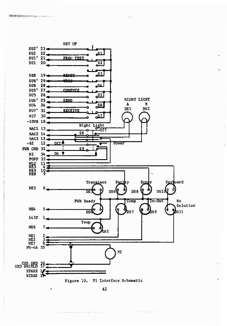
The control panel interface with the Main Computer consists of 4 cannon connectors Pi, P2, P5, P6 and a wiring harness connecting the power on-off switch, night lights, running time meter, set up but- tons, reset button, neon NIXIES, input matrix, keyboard and mechani- cal reader to these connectors as indicated in figure 9.
1. Power Control
A schematic of the Pi interface with the set-up buttons, re- set button, night lights, power on-off switch, neons and running time meter is shown in figure 10. This plug mates with J20 on the main com- puter chassis. The power on-off switch is shown with a -6 volts and power GND feeding back into POFF and N2 respectively in the ON posi- tion. In the OFF position, these are removed and a ground is placed on the power OFF input. The inputs to the night light are approximately 7 volts AC for each, and the input to the time meter is 120 volts AC, from the computer, after the main power relay is held on.
2. Set-Up Buttons
The set-up buttons are energized with a -10 volts from the computer main chassis and supply a -10V "ON" signal (or an open "OFF") to SU1, SU2, SU4, SU5, SU6, SU7 in the "ON" positions and toSUl-, SU2', SIM', SUB', SUb', SU7' in the "OFF" conditions. Along with the SUO, SUO', SU3, and SU3' signals from the keyboard these signals are connected to the following matrix circuit in the main com- puter chassis (figure 11).
4]
wMMUiiMtbMrJMi
•
sua1 SU2 sur sui
SER sue1 SU6 SUS' sus
SU4 su?' SU7 -10VB
6AC1 6AC2 6AC3
-6Z PWR GND
N2 POFF NLC NE3 NE9 NE8
NE5
NE4
U3Z
NE6
NE1 NE2 NE7 PH-4A
23 22 21 20
19 29 28 27 26 25 24 31 30 18
13 14 15 12 32, 34, 33.
10 9
5*-
7«.
2, 3.
35
CHS GRD GRD SHIELD
SPARE WIRES
SET UP
PROG TEST "id
9SUU TRIO
comas
sm- Ä—f— ■« i»
RECEIVE o£z]
Night Light
NIGHT LIGHT A B
DS1 DS2
-o-r -fcHsOrtte-
Qit*
On ♦ Jäl o—t-
Power
ieady l~~H *tcomp *_Jln"c
Temp
V^SS
Kgxjoard
DS1(0 Ih-Out 1 No
> ""N Solution
(JjA is ii
? MI
Figure 10. Pi Interface Schematic
42
*SU3
SU4 SU5 sue SU7
Remote Receive ESU2
*SU2
SU2 SU3 SU6 SU7
Remote
4.7K
Receive Receive L^ m ESU2 ESU2 ^ ]
*SU1 *SU2 *SU3
*SÜ
♦SU1
Figure 11. "Operation" Switches Computer Interface
43
3. Keyboard
A schematic of the P2 interface which is wired to the key- board and mechanical reader is shown in figure 12. The plug mates with J21 on the main computer chassis. A schematic of the manual keyboard with the interface circuits in the main computer chassis to which it mates is shown in figure 13, This is a representation of a mechanical keyboard.
When the enable line is energized and a key is depressed, the solenoid is energized, allowing the appropriate information lines for that key to be energized. A cycle of information, strobe, and strobe' pulses results as shown in figure 14.
An electrical interlock is arranged such that only one such cycle will result as long as the key is depressed even if the enable line is de-energized and then energized again. A mechanical interlock is also incorporated so that one and only one key can be depressed at a time. The SM (SUO) and the RECALL (SU3) portion of the keyboard have been previously described.
4. Mechanical Reader
A schematic of the Mechanical Reader circuitry is shown in figure 15, along with the types of paper tape used. Schematic repre- sentation is also made of the circuit interface existing in the computer main chassis.
The enable signal (MGROS) energizes the solenoid when a tape is inserted (MRL) and excessive tension is not present (tight tape). A sprocket wheel inserted in t-le sprocket holes of the tape rotates the tape and creates the cycle of pulses shown in figure 16. The informa- tion contacts are closed mechanically by spring loaded fingers when a hole exists in tape. The computer de-energizes the enable line upon receipt of the RCC contact or TC signal and cannot energize again until several word times after the B contact or TC goes true again. A cycle of information, strobe, and strobe1 pulses is shown in figure 16.
The computer can accept the maxin vm free running rate of the mechanical reader, during a manually initiated continuous reading cycle, which is 20 to 35 lines per second. However, under program control where other programming is accomplished between readings the speeds may be much slower.
44
NOT USED
PWR GRD
KEYBOARD
I7C I8C TC
CHS GRD
» NOT
NOT USED MR1
N
€
MECHANICAL READER LAZ1
rS m
i 4L.
+••3
NOT USED MRL -18V
'NOT USED
SPARE
PWR.GRD SUS' SU3 SUO. SUO1
TCK' GRD
^L8 I1C *•
- ■ -32VB GROHIELD
Figure 12. P2 Interface Schematic
45
Functional Representation of Keyboard
CR1
Sw.
ni jSolenoid
I -f-
A*
JLZ
Computer Interface
•> K12 -31VDC
KCC—f
KCl
KC2
KC3
KCA
KC5
KC6
KC7 ..JTZZ
KC8
SM
RECALL
CR2--
•18V
22K
TCR* -»■ K15 GND TT5v
-♦ K23 -18V
K9 TC Kll -10V
■+T3v:
Ki no
.7K
K2
K3
K4
K5 +15V
-m- K6
♦ K7 m Kg I8C
-m- K14 GND
♦ K16 SUO
4.7K
K18 SUO' *Arrestor --•- K19 SU3
■" K21 SU31
Figure 13. Keyboard Functional Diagram
46
.'fciU«ipr«rti. ■ ■
I 25 ± 15 I MILLISECOND?
True
Pin 9. (TC) False
I Time required to consume ^N all bounce that may occur 1-1- Max, Time shall not exceed 257. of actual TC tine.
Min. time shall be greater than actual TC time and Max time shall not exceed 25% | of actual TC time.
X True Pin 10. (TCK1)
.Critical period when TCK* must not bounce
True
Information lines Pins 1,2,3,4,5,6,7&8 False
True
False-
Code sampling period Indicates a closed circuit condition at the corresponding pin numbers. Indicates an open circuit condition at the corresponding pin numbers.
Figure 14. Keyboard Timing Sequence
47
■:;
MRGOOS »<♦- URL >•<•
TC >'<■
TCR'ss«
IN647 330 ohms,VW
1 1 D»IVt | 1 SCHENOIO
[c cl
• \JND «TC
(NO TA«)
ND iv NC
(TIGHT TAPE)
8 lEVEt TAPE
O o o
8 7 6 5 4% 3 2 \ OOOO 00 ooo o
o o o
lEvei TAPE
TYPE II
FEED HOLE
Figure 15. Mechanical Reader Functional Description
48
Forward
Input Drive
Solenoid Armature Displacement
Contact B
Contact B'
Contact RCC
Contact RCC1
Contact RC1 thru RC8
I L
Start One Read* Cycle J
Critical period «hen |B or B* shall not
I bounce
I I
End
Figure 16. Mechanical Reader Timing Sequence
49
/
The manually initiated fill mode is applicable to both the Keyboard and Mechanical Reader. In each case the computer is forced into manual halt by GPRC (-10V) and GPHC (+6V) on the input plug J17. For the Keyboard input the RECEIVE button on the computer is first depressed then -10V is momentarily placed on FBPR (FILL button) on the input plug J17, This places the computer in the Keyboard input mode. Only the octal format by word is accepted in this mode. For the Mechanical Reader, the RECALL button is first depressed and the -I0V is momentarily placed on FBPR. This places the computer in the me- chanical reader input mode. Again the octal format by word is the only one accepted, however, either TT or FIELDATA code is applicable by leaving MRTT open for Teletype and grounding MRTT for FIELDATA input.
In the FIELDATA input mode only the FIELDATA paper tape code format is accepted by the Mechanical Reader. Additional informa- tion related to the Manually initiated fill mode is contained in Section IV.
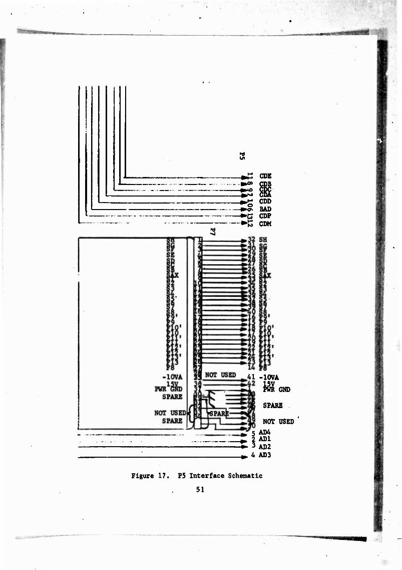
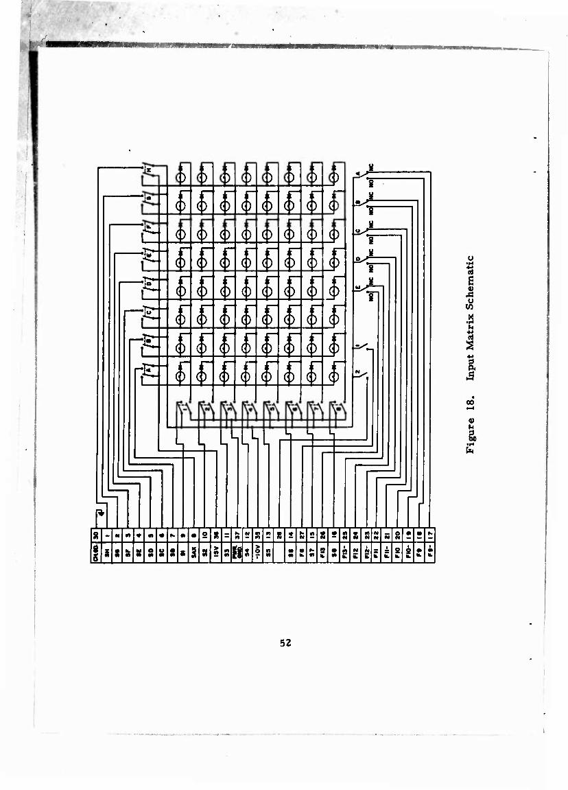
The wiring schematic of the P5 interface showing connections to the NIXIES and the Input Matrix is shown in figure 17, and indicates the computer interface with which these contacts mate in the computer. A schematic of the Input Matrix is shown in figure 18.
5. Input Matrix «.
The Matrix input device serves to input particular combina- tions of bits into the A-register upon use of the DIA (Discrete Input into Accumulator) command.
The device has a column of 8 push-buttons (A to H) and a row of 8 push-buttons (1 to 8). In addition, there are 5 push-buttons labeled A through E, norr ally referred to as the battery buttons and 2 push- buttons labeled 1 and 2, normally referred to as the weapon type buttons. The 8x8 push button arrangement provides information to the computer of the 64 different combinations of bits designated F2 through F7.
An Fl bit is used to indicate that a push button is depressed in both the row and the column. The five battery buttons supply infor- mation to the computer of the bits F9, F10, FU, F12, F13 and are normally used to associate with a particular battery in the artillery
50
!
en
CDE IB •»oo COB
-•»^i CEA ^^ ODD -^S BAD -^G CDP ^ß CUM
41 -10VA
i. 2 AD1 ► 3 AD2
15V PWR GND
SPARE
NOT USED
5 AD4
^ 4 AD3
Figure 17. P5 Interface Schematic
51
.
1 '
nE-
£l£l£L£
; r ()
()
()
II
; r i>.
i r o
C)
()
II
; r
l"
l"
iT
r C) ;; ()
ii
iT
; r it
; r SL
IT
iT 0
£ t
: r
r
r
£1 o
()
ii C)
t
mn" Si iT
i"
_$.
iT
iT ()
()
ii
()
n () C)
£J ii
if* ()
■,i~
()
if J) ;T ()
T ^L T JL T
T JL
() li
C)
e ü y
H
ä
v
£l i 5 8
> « IIS in
B k.
52
problem. The two push buttons labeled 1 and 2 supply the F8 bit either on or off to the computer and are used in the artillery problem to asso- ciate with a particular weapon type.
The 8x8 push button array has a removable template which designates by a light the associated programmed function of each of the 64 positions. The template is easily changed and a new one may be de- signed for any particular application or program. The information bits supplied by the matrix to the computer, Fl through F13, are sampled by the DIA command and placed in the A-register from which they can be interpreted for the particular function the computer is to perform.
The bit designations Fl through F13 are hardware designa- tions and differ from those in the programming manual. Fl here re- fers to the least significant bit of the word which occurs at Tl time whereas in the programming manual this bit is given the F31 designa- tion. The assigning of bit locations as applied to programming posi- tions versus hardware positions is further defined in Section IV, Para- graph B. 2. f.
6. NIXIE Readout
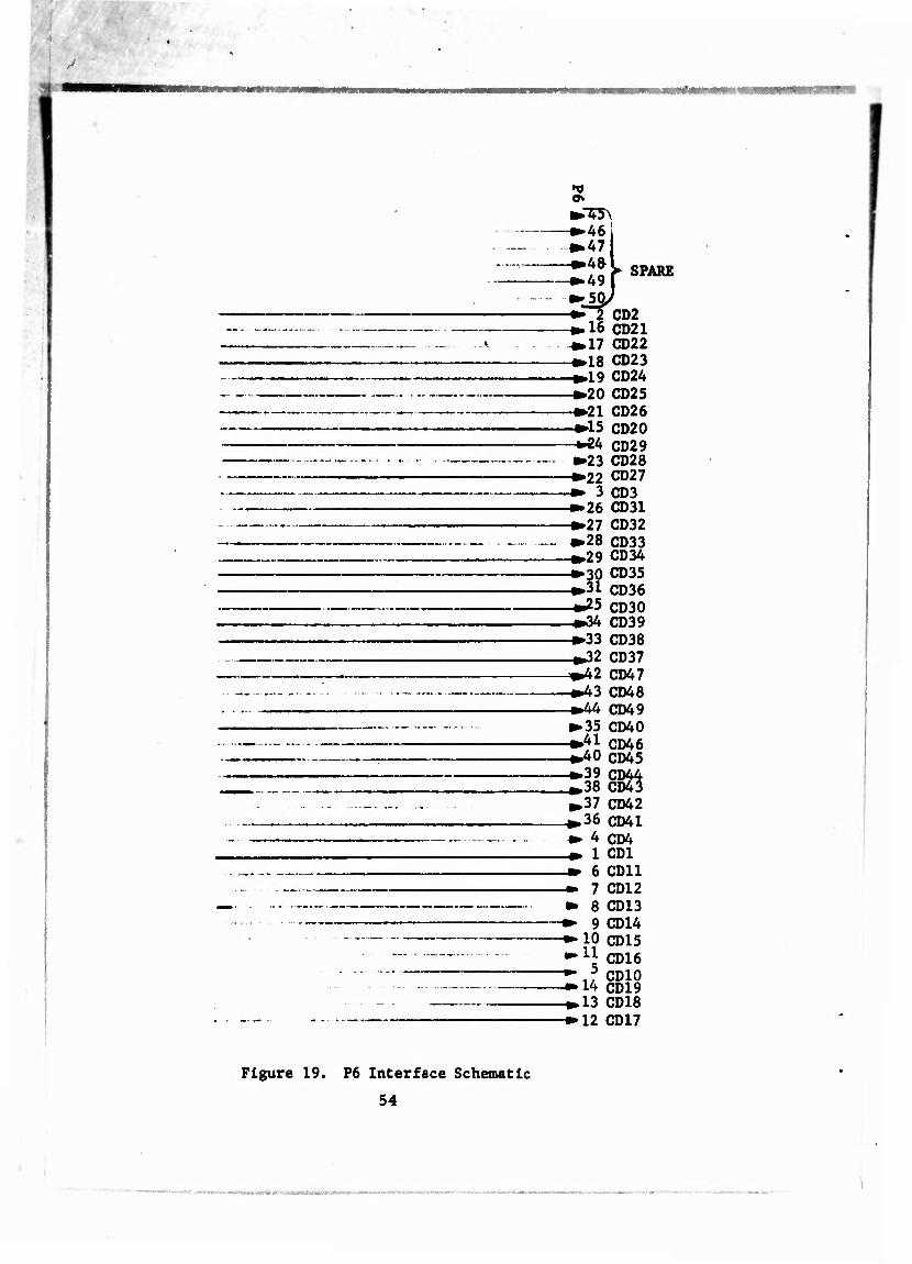
The wiring schematic of P6 for the NIXIE indicators on the control panel is shown in figure 19.
Of the eighteen NIXIES shown in figure 20, one NIXIE serves as the Battery indicator. The seventeen remaining NIXIES represent 16 decimal digits of information from the "D" register, with the "SIGN" and "CHARGE" sharing a NIXIE. The cathode driver is the same as for the Battery NIXIES and is shown in figure 22. The anode driver is shown in figure 21.
Four anode drivers, each energizing four NIXIES, are cy- cled each 1/4 revolution of the memory disk. This rate provides the effect of flicker free lighting of the full NIXIE complement.
A readout schematic is shown in figure 23, and display ar- rangement in figure 24. A functional wire listing is described in figure 25.
53
am
Ov
-»>46
-»48 -»•49
•50
► SPARE
*^2 ( _ CD2 P. 16 CD21 »17 CD22 -»18 CD23 -»19 CD24 -»20 CD25 -»21 CD26 -»15 CD20 —*»Ä4 CD29 »23 CD28
-»22 CD27 -»• 3 CD3 -»26 CD31 -»27 CD32 »28 CD33 _^29 CD34 -»30 CD35 -»31 CD36 -*25 CD30 -»34 CD39 -»33 CD38 -»32 CD37 -»42 CD47 -»43 CD48 —»44 CD49 »35 CD40 -»^i CD46 -»40 CD45
»37 CD42 -»36 CD41 »■ 4 CD4
1 6 7
GDI CDU GDI 2
» 8 CD13 ♦ 9 CD14 ♦ 10 CD15 ••1J CD16
'*' * CD10 -• 14 GDI9 -»13 GD18 -♦12 GD17
Figure 19. P6 Interface Schematic
54
u 01
i ** eo
ll -H i M 01
* o. o
<-* tfa
1 Cb <-> 1 •H •^ 1 r-l e i 1
■ fe s 1 ^ « u I <-* 4 1 a. T w C f
i «J «■ o S 1 u
•H 1 PO
VO 1 r-l
f« Ü PQ >%
0) Al
s X
PQ
I n
o
a,
pojg
55
i
# +155V
« +143Z
Figure 21. NIXIE Aftode Driver
Input Gate •>
2N738
Output
Figure 22. NDCIE Cathode Driver
56
«rs
Network "B"
406
407
408
409
Pin
F9
F10
Fll
F12
55B
Bat in
BDX
BDX
BDX
BDX
44B
X in
CATHODE DRIVERS CD
PIN
406
407
408
BAT.
52A
CDA
CDB
CDC
DPL2
DML3
F13
57B
L3 or L2
L2 or L3
DSU2
DSlb
BDX
51B
U2 In U2
DSU2
268
02 out U2
DA4
D4
D8
26A
K4 In
Ü2
CD
Ü3 Lo
CDx
SIGN & BAT. DEC FT
54A 23B
CDP CD1D
CDM CD2D
CDE CD3D
Ü2
CD
± K9
23A
CD19
CD29
CD39
DA3
nA7
D3
D7
288
U2 yu;
DPL2
33A
tJ.Z out t2
Ja ^ 02 ,L0 Ul L3
CD CD
„L
JK8
24A
CD18
CD28
CD38
JK7
28A
CD17
CD27
CD37
409 ODD CD4D CDM CD48 CD47
^
DA4 BA3 DPL2 DA2 DAI DML3 DAA* DA31
-Ma. D4
D8
26A
K4 In
JiLL
-BL
288 33A
DA6
D2
D6
34A
Ml, Dl
D5
AQA 32A
DA81
DU*
DB'
43A
DA?1
D31
07'
41A
Figure 23. NDCIE Readout Schematic
b 57
DAS'
DA?1
03*
D?«
4U
L3 Uoi |L2 !
CD
■i < <■»
DA2'
DAS'
02'
06'
49B
K2' In
DAI1
DAS'
Dl'
DS'
57A
Kl' In
i^jTi
-:--, VS. JL
CD
M ho
CD
K2
45A
CD12
CD22
CD32
CD42
^1
48A
CPU
CD21
CD31
CD41
KQ
SPA
gpio
CD20
CD30
CD40
XI1
XI
XI'
XI
1A
X21
_X2^
X2
X2
IB
A torn InlLini
NXD
NXD
NXD
NXn
2A
AMODE DRIVER
A Out
3B
API
AD2
AD3
AD4
■18N
40B
■m. -18N
-18N
-18N
-15V
3A
-15V
-15V
-15V
+78Z
38B
iZSi. +78Z
+78Z
+78Z
| KO 00 21. 00 Uo LO I
I Kl 00 01 UO LI 1
1 K2 00 10 UO L2 1 1 K3 00 11 UO L3 1
1 K4 01 00 Ul Lol
\ K5 01 01 Ul LI 1 i K6 01 10 Ul L2|
1 K7 01 11 Ul LSI ! K8 10 00 U2 Lol
K9 10 OV U2 LI
1 + 10 10 U2 L2
1 - 10 11 U2 L3I 1 * 11 00 U3 Lol
1 Blank 11 11 1 U3 L31
»155V
56B
f-155Y
fl55V
fl55V
H55V
+66Z_^8iL
4B
+m. 466Z
+66Z
+66Z
58B
m H8V
18V
•ISV
+1^Z
Jih.
+14iZ
+uiz +iÄiz
t
o.
Btry ± Chg
0 0 0 J4 J5 J6 J8 J9
AZ
>-Fuze Set ^ime of Fit.
Jl( J7 ji JI; JI:
Distance
.Quadrant n JI/JKJI: jiui
^ —Vert Angle—/ Easting ) I Northing _J L_ Altitude )
LSB n TTTTTI ^~y[2 Jrt JK jiß Jtf JW JT5 J2VJÜ
n n Ml
Nixie Code Bit 0 0 0 0 0 1 0 Q 0 i 2 0 Ö I 5 3 0 0. L ^ n 1 0 Q. 5 0 1 0 1, 6 0 0 7 Q 1 8 ,9, ,9,, s 0 0 0 1 + ,0 o
1 9 \ 1 • .1 Q o
Rlank ± LX
Figure 24. NIXIE Display Arrangement
59
PIN FUNCTION PIN FUNCTION PIN FUNCTION
1 Spare 1 Spare 1 CD input Dec. Pt
2 Spare 2 Spare 2 Spare
3 Spare 3 Spare 3 CD input 1
U CD Input C 4 Spare 4 CD input 2
5 CD Input B 5 Spare 5 CD input 3
6 Spare 6 CD input - S CD input 4
7 CD input E 7 Spare 7 CD input 5
8 Spare 8 CD input + 8 CD input 6
9 Spare 9 Spare 9 AD input
10 Spare 10 Spare 10 Spare
11 AD input 11 AD input 11 AD input
12 CD input D 12 Spare 12 CD input 0
13 Spare 13 Spare 13 CD input 9
Ik CD input A 14 Spare 14 CD input 8
15 Spare 15 Spare 15 CD input 7
Jl BATTERY NIXIE J2 1 NIXIE J3 THRU J18 NUMERICAL NIXIE
Figure 25. Cathode Driver (CD) and Anode Driver (AD) Connections to NIXIE Display
The information is read from the two word D loop 16 bits at a time shifted into Dj through Dg and DA^ through DAg , When the shift is complete, the anode driver is enabled and the 4 NIXIES light up with a cathode selected by a matrix from the 16 bits. When the sign is ON, the charge NIXIE is OFF and when a charge digit is energized, the sign is OFF.
60
■
IV. EXTERNAL INPUT-OUTPUT INTERFACE DESCRIPTION
A. General
Interfacing to the FADAC can be established for a variety of peripheral devices by the proper connections to the computer. The Input-Output interface is accommodated by an Input connector, J17, and an Output connector, J10. Both of these connectors are mounted on the computer main frame as indicated in figure 1, and in figure 2.
When an Input signal is described as "TRUE", "ON", or a "1", it is defined as a signal of -3V ±1V, into 150 ohms. An Input logic term of "FALSE", "OFF", or a Mi ohms. An Output term of "TRUE" nal of -6V through 150 ohms. An Output term of "FALSE", "OFF", or a "0" is defined as -6V through 100k ohms. These are the normal logic signal levels utilized unless otherwise specified. Figure 26 schemati- cally illustrates am Input amplifier, an Output amplifier is schematically shown in figure 27.
, it is defined as 0V ± IV into 150 "ON", or a "0" is defined as a sig-
ON - -3±1 volt
OFF - Open or Ground
330 Input Impedance is 150 ohms; 0.001 microfarad to ground
Figure 26. Input Driver
61
»
100 ohms out
ON - Output transistor saturated
OFF - Output transistor Cut-off
Figure 27. Output Driver
Communication, in addition to data lines, between the Input de- vice and the M18 computer is also accommodated by J17. Therefore, even though J17 is used primarily for inputting, there are several out- put signals available from J17 to provide effective Input device inter- facing. On the same premise, communication, in addition to data lines, between the output device and the Ml8 computer is also provided by J10. This requires that the primarily outputting J10 receives several input signals to provide effective MIS to Output device interfacing.
Figure 28 is a schematic presentation of Inverters that are of a type common to both Input and Output operations.
out I0B
+6V
Figure 28. Inverter
62
■ ■
B. Detailed Input Description
1. Input Terms to GDC, M18
Connector J17 is a Bendix-Scintilla Type PTOOSE-24-6lS(005), that is mounted on the left side of the computer main frame and requires a similar plug type connector for mating. J17 is provided for intercon- necting the computer with peripheral input devices. The signals on J17 are listed in Table II, that reveals that most of the lines connected to J17 are input lines.
A schematic presentation of J17 is shown in figure 29.
.•!
Table II. DESCRIPTION OF TERMS ON J17
Term
I1G l?.C I3G I4G 15 G 16 G 17 G I8G
TG
Description
TG'
TGO'
TEIP
MTF
Data Input Lines to GDC M18 in 8-level Alpha-numeric or 5-level Teletype.
An input to GDC Ml8. This term is used for strobing of the Input Data Lines IlG through I8G. This term can be configured in alternate ways and is further described in paragraph IV, B.2.b.
Refer to TG.
Inverted TG1. From an output driver.
An output from GDC M18. This term is used in conjunction with information input. TEIP is the inverse of the TG signal.
An input to M18. With the MTF line open, the M18 is in the "INPUT" mode; ground, in the "VERIFY" mode.
63
- -r—•^-'"'fiMllrliiriümM
/
Table II. (Cont'd)
Term Description
IFS Determine parity to be sensed. If open, input data is odd parity tested; if ground, input is even parity tested.
FBIO An output from GDC MI8, to an input device. This term is normally false. FBIO goes true when the M18 is in the mode to sample the information on the input lines. This signal re- turns to the false state when TEI* goes true. Maximum in- formation to and from Ml8 is dependent on the type of infor- mation transferred. Maximum rates are:
RGO
4000 characters per second in a/n 6 mode 3500 characters per second in a/n 5 mode 500 characters per second in Octal or Decimal mode.
This output signal goes true when FADAC is in an "INPUT EXTERNAL DEVICE" condition.
RHO Inverse of RGO, When FADAC goes out of the RGO mode, output term RHO goes true.
RDYO Inverted FBIO, gated with "INPUT EXTERNAL DEVICE". This output term comes true only when FADAC is in the "INPUT EXTERNAL DEVICE" mode.
PEO Parity error output, curred.
When "TRUE" a parity error has oc-
OPL4 Discrete output lines. OPL4 is activated by operation Code OPL5 3710, OPL5 by 3712, OPL6 by 3714. Only one OPL r>ay be OPL6 selected at one time. Selected OPL will be turned off by
subsequent selection of another OPL, or by the DOF (3700) command. The OPL lines output Drivers are schematically presented in figure 27.
GPRC An input to MIS. This term is conjunction with the GPHC controls the "RUN-HALT" mode of the computer. With an open circuit, the computer is in the "RUN" mode; with -10.0 ±1V applied, the computer is in "HALT" mode.
64
Table II. (Cont'd)
Ter m Description
GPHC An input to M18. This term in conjunction with GPRC con- trols the "RUN-HALT" mode of the computer. With am open circuit, the computer is in the "RUN" mode; with +6 ± IV applied, the computer is in the "HALT" mode.
FBPR
F25I F26I F27I F28I F29I F30I
F25 F26 F27 F28 F29 F30
An input to MIS. Initiates Octal input when computer is in manual Halt mode. Normally false (clamped to 0.0 ±5V) FBPR is -10. 0 ± IV when true.
Inputs to GDC MIS. These terms are sampled into the "A" register under program control. A one-to-one correspondence exists between the F subscripts and the corresponding bit po- sitions of the "A" register. The programming bit position notation versus hardware notation is described in Section IV. B.2.f.
Outputs from the F25I through F30I input amplifiers.
GND PWR Power Ground.
GND CH Chassis Ground.
-35V -35V Supply.
+35V1 These voltages energize the appropriate write switches allow- + 35V2 ing the computer to write into "COLD" storage and, therefore, +35V3 all 8, 192 words of memory.*
143Z +143 volt zener - regulated supply.
-3V -3V regulated supply.
See end of table.
65
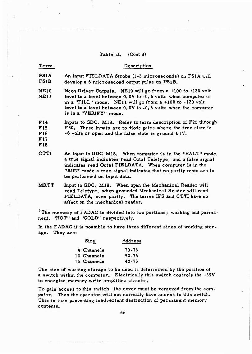
Table II. (Cont'd)
Term
PS1A PS1B
NEIO NEU
F14 F15 F16 F17 F18
CTTI
MRTT
Description
An input FIELDATA Strobe (1-2 microseconds) on PS1A will develop a 6 microsecond output pulse on PSlB.
Neon Driver Outputs. NEIO will go from a +100 to +120 volt level to a level between 0. 0V to -0. 6 volts when computer is in a "FILL" mode. NEU will go from a +100 to +120 volt level to a level between 0. 0V to -0. 6 volts when the computer is in a "VERIFY" mode.
Inputs to GDC, M18. Refer to term description of F25 through F30. These inputs are to diode gates where the true state is -6 volts or open and the false state is ground + IV.
An Input to GDC M18. When computer is in the "HALT" mode, a true signal indicates read Octal Teletype; and a false signal indicates read Octal FIELDATA. When computer is in the "RUN" mode a true signal indicates that no parity tests are to be performed on Input data.
Input to GDC, MIS. When open the Mechanical Reader will read Teletype, when grounded Mechanical Reader will read FIELDATA, even parity. The terms IFS and CTTI have no affect on the mechanical reader.
The memory of FADAC is divided into two portions; working and perma- nent, "HOT" and "COLD" respectively.
In the FADAC it is possible to have three different sizes of working stor- age. They are:
Size
4 Channels 12 Channels 16 Channels
Address
70-76 50-76 40-76
The size of working storage to be used is determined by the position of a switch within the computer. Electrically this switch controls the +35V to energize memory write amplifier circuits.
To gain access to this switch, the cover must be removed from the com- puter. Thus the operator will not normally have access to this switch. This in turn preventing inadvertent destruction of permanent memory contents.
66
k
0 a
T4 60
CM
A
o
c
es fa
k
0
M VO CM (14
A A
a. •M
CM CM fa fa
cr »n
fa oo CM fa
0
u
00 CM fa
o
.*
CM fa
CM fa
CM co ^ m vO t^
A
o
e
3 «n fa
o CO fa
a >
^
AAAAAAAAAA n
o
fa
o
pa a
o
M fa
O
Ü
o
SB
o
*1
J 0
h4
Ö
X fa Pa
6
»
6
o
r«.
m
s
ON
CM
S> fa
.i.
4) H
Ü Ü o i-i CM en H H H
Ü
H
O in H H H § 12 Ü
H
fa H -
67
' /
I ■ 1
/
to
A 4)
2 « i > ( ) c 3 i > V } (. ► > i > J o Ö 0 o ö o
& 04
ig
> m in i-t CM *n N > ft * *>
IT» CO > r-4 r-lrHr-l^lDvOrxOO
+ + + + + IPU &ggCMbPXMpt4
M r»
S > NU Ü 00
|-A/VV#(*
I i-i
Ö
5-wv->^ I a
ON CM
I
I I I 0 > O H PQ
6
o
CM CM
5-wv>-
o H
0 o
p 8 g 9 ^
O '^ o
o o o ass § & §
us CM«
CM<
S-AAAr-#-J
1 6
O I PQ
68
2. Input Circuitry
a. Input Data Lines - The input information to the M18 com- puter is accepted on the "I" lines. These lines, II through 18, are ap- plied to eight corresponding input drivers. A schematic presentation of these drivers is shown in figure 26.
b. Strobe - The normal strobe for data input on I1G through I8G is TG. The information and strobe pulses are similar to those in figure 30. FBIO is not required unless operating at or above the maxi- mum input rate. Figure 31 shows a typical input wiring configuration.
DATA ("I") LINES
0
1 r STROBE
(TG) 0 -
6 Microseconds Minimum
FEEDBACK (FBIO)
0
Figure 30. Input Line Timing
69
I
FADAC
I1G •
I2G .
I3G
I4G
I5G •
I6G •
I7G -
I8G .
TG -
TEIP-
TR' .
FBIO-
RGO
IFS
CH GNBL
CTTI-
-3V -
PECO.
+138Z.
NE10
NE11-
GPRC1
GPHC2I FBPIL.
^■
-^
4-
Extemal Inputting Device
FADAC Strobe
^i
^
.Neon Supply
, -v, For External - ^Halt and "J Fill Control
Figure 31. Inputting to FADAC
70
-■-(^iJliWi'.jäiii ti
,
Other input devices can be accepted by the M18 computer as long as the "ON-OFF" voltage conditions and the rate of the input strobing action is compatible with the computer interface. Only one de- vice at a time can be accepted by the computer and external switching must be provided to select the device applicable at that time. The ex- ternal device strobe input to rhe M18 computer may be of the method described or one of the following two methods may be employed: A steady state strobe by connecting one strobe line to TG with TEIP (the inverted TG signal) shorted back to TR* as figure 32. Where the strobe and strobe' consists of an on-off contact with inherent contact "BOUNCE" the connection should be that as shown in figure 33 to compensate for the "BOUNCE".
c. PSl Pulse Stretcher - The normal strobe for input data must be a minimum of 6 microseconds as characterized by TG. In the event that a shorter time duration strobe is to be employed, such as the 2 microsecond FIELDATA strobe, this strobe must be expanded. PSl may be utilized to condition and expand this strobe to the required 6 microseconds.
A short strobe applied to the PS1A (pin DD) will trigger a 6 microsecond monostable multivibrator in the M18. The output of this multivibrator appears at PSlB (pin EE). Connection of this PS1B output to TG will then provide a compatible strobe for the input data, with the timing relationship as indicated in figure 34.
The trigger and multivibrator circuit of PSl is displayed schematically in figure 35.
d. Neon Drivers - The MIS computer contains two types of neon drivers. Type 1 of figure 36 is the driver employed for the following neon indicators:
(1) Compute, NE1
(2) In-Out, NE2
(3) Pwr Ready, NE4
(4) Fill, NE10
(5) Verify, NEU
71
I V ■ AW •
GDC M18
Strobe Input TG
J17
Tl
TEIP
External Connection
TR'
R
Strobe Width
Strobe Period
6.0 microseconds
249 microseconds (For Alphanumerics) 1590 microseconds (For Numerics)
Figure 32. Steady State Strobe
72
Strobe and Strobe1
with contact bounce
TG
I I GDC M18
I J17 |
M
-3V
TG1 N I
External Connection
TR'
Strobe Width 6.0 microseconds 7.5 microseconds
Strobe Period 249 microseconds (For Alphanumerlcs) 1590 microseconds (For Numerics)
Figure 33. Mechanical Contact Strobe
73
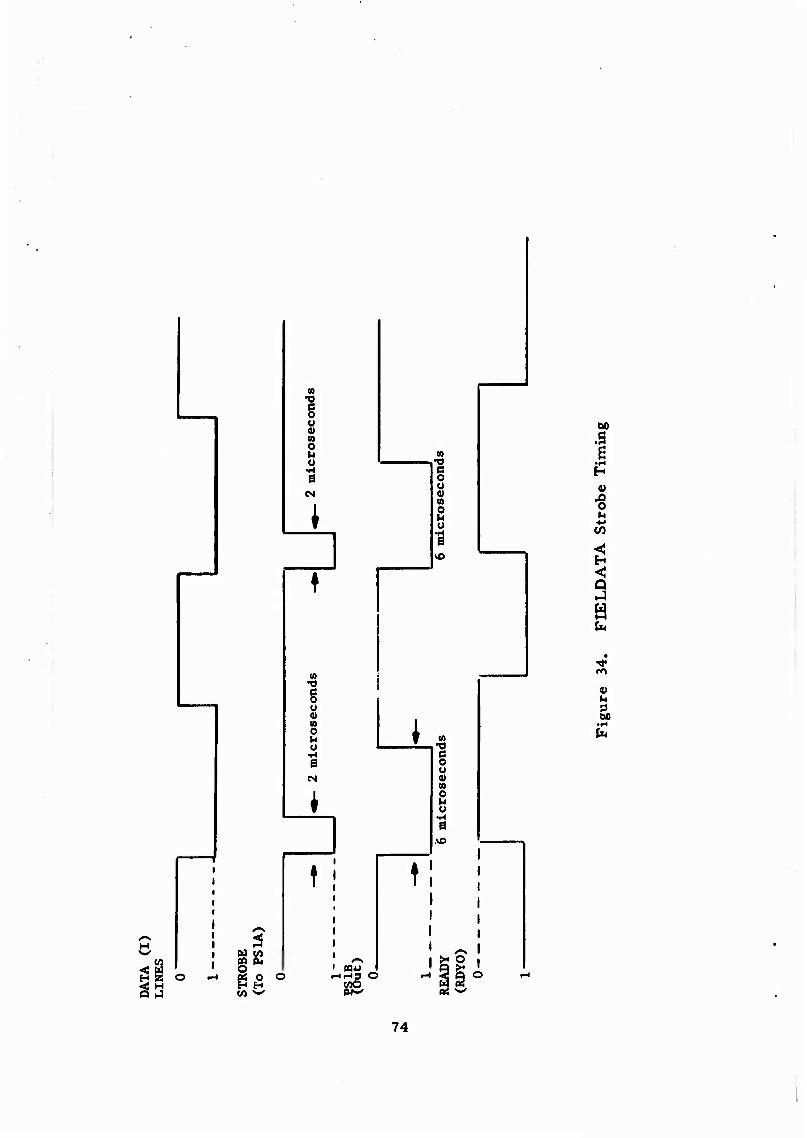
CO
1 u (0 o t-l o
CM
I
CO •O e o ü 4) W
s u
vO
00
I U
In
o 9i CO o m u
•H 6
I CO •O C o u 0) CO o u a
.vO
4)
^3
^J2 PQ Q
t
- B M
CQ4J •-ii-iS o
74
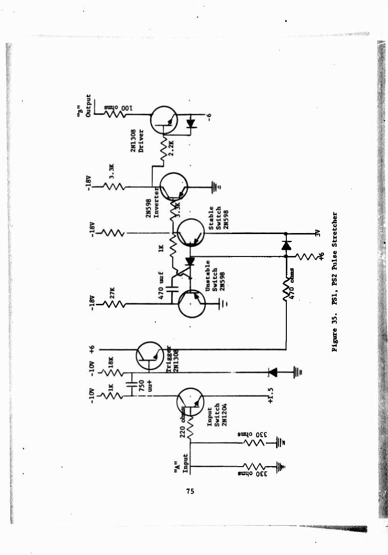
'"'-
-ft
I u 4J 0) u u
CO
g^VW
CM
en 01
smqo oe€ .
V\Ar^ll•, wnqo o€C
75
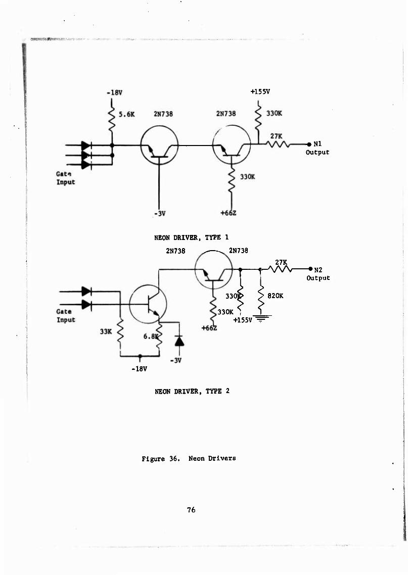
■
+155V
• Nl Output
NEON DRIVER, TYPE 1
2N738 ^—^ 2N738
330j
27K -•N2 Output
820K
330K 1 +155V ~
• ISV
NEON DRIVER, TYPE 2
Figure 36. Neon Drivers
76
* ■»■..- »
Two type 1 neon drivers are available at J17, pins FF and GG, NE10 and NEU, respectively.
The type 2 neon driver of figure 36, is employed for the following neon indicators:
(1) Transient, NE
(2) Temperature, NE
(3) No Solution, NE
(4) Parity, NE
(5) Overflow, NE
e. Discrete Input (F) Lines - The information bits supplied by the Input Matrix, Section III, Paragraph 8-5, and the discrete input lines on J17 are sampled by the DIA command for placement into the "A" register. In this case the designation Fl through F13 from the Input Matrix, and F14 through F18, F25 through F30 of J17 are "HARD- WARE" bit positions.
It must be noted that these hardware designations differ from those of the "PROGRAMMING" notations.
Fl in hardware refers to the least significant bit of the word which occurs at Tl time whereas in the programming manual this bit is defined as F31.
A correlation between programming and hardware nota- Ition is presented in figure 37. The definition of a given bit position
must therefore be qualified as to whether it is a program or a hardware reference.
F25I through F30I are applied to input drivers as indicated in figure 26.
77
IfW-
HARDWARE BIT POSITIONS
3231 T JO I r
28 F b P p r P p- 27^6 25^2322 2]
Trrr 20 1*1817 L6 B 14 1312 1110 9 p 7 6 5
rrrr 4 3 2
T 1
0 i 2 3 4 5 6 7 8 9 10 i. E 1314|l5 L6|L7 lil9J0!l 12 23 J4 2526 27 282930 31
E CONTENTS OF WORD
PROGRAM BIT POSITIONS
Figure 37. FADAC Bit Positions
C. Detailed Output Description
1. Output Terms
Output connector, J10, is a Bendix-Scintilla Connector PTOOSE-22-555Y(005) mounted on the right side of the computer main frame and requires a similar connector for mating. J10 is provided for interconnecting the M18 computer with peripheral output devices.
The signals on J10 are listed in Table III, indicating that most of the lines connected to J10 are output lines.
A schematic presentation of JIG is shown in figure 38.
2. Output Circuitry
a. Output Data Lines - The output information from the M18 computer is provided on the eight "D" lines. These eight lines, D100 through D800, are supplied by eight corresponding output ampli- fiers as shown in figure 27, The output timing is displayed in figure
39.
78
r '
Table III. DESCRIPTION OF TERMS ON JIO
Term
D100 D200 D300 D400 D500 D600 D700 D800
AMTO
IM TO
FBOO
STBO
OPL1 OPL2 OPL3
Description
Output lines from GDC, Ml8 transmitting 8 level Alpha- numeric or 5 level Teletype information.
FTF
EER
ESU
OPE
Output from Ml8. This normally false term is true during a/n 5, a/n 4, and Decimal output modes.
Output from Ml8. This normally false term is true during Octal and a/n 6 output and a/n 6 input modes.
This M18 output term indicates when information is present on the output lines: D100 through D800.
1 to 2 microsecond output pulse indicating when information is present on output lines, D100 through D800.
Discrete Output Lines. OPL1 is activated by operation code 3702, OPL2 by 3704, and OPL3 by 3706. Only one OPL may be selected at one time. Selected OPL will be turned off by subsequent selection of another OPL, or by the DOF (3700) command. The OPL lines output drivers are schematically presented in figure 27.
This term must be grounded to permit FADAC to FADAC data transfer.
This "ERROR RESET" input signal clears the error light and resets the computer. Computer is put into a "HALT" mode.
Activation of this Input term while computer is in program halt mode will cause the transfer of control to the "RECEIVE" button location (Channel 00, Sector 007).
Activation of this input term causes all the "D" output lines to assume "O" state. True state is -6 volts or open, false state is ground ± 1 volt.
79
Table III. (Cont'd)
Term Description
OFS
TFAI' TFAO» TIBO' TFBO
TEOP
F19I F20I F21I F22I F23I F24I
F19 F20 F21 F22 F23 F24
PS2A PS2B
EER20 ESU20
CLKD STRD
An input to Ml8 that determines computer output parity. If grounded, output data is "EVEN" parity*; if open, output data is "ODD" parity.
Inputs to M18. These terms are feedback signals from some external device. These terms for strobing output data can be configured in alternate methods as described in paragraph C. 2 of Section IV.
An M18 output term that is the inverse of TFBO'. This term is used in conjunction with information output.
Inputs to GDC, MIS. These terms are sampled into the "A" register under program control. A one-to-one correspondence exists between the F subscripts and the corresponding bit po- sitions of the "A" register. The programming bit position versus the hardware notation is described in paragraph IV. B.2.f.
Outputs from the F19I through F24I input amplifiers.
At the time that Input PS2A goes to ground, output PS2B will go to -3V from its normal ground level for a period of 6 microseconds. A schematic of this "PULSE STRETCHER" is presented in figure 35.
Ml8 Output Signals used primarily in FALT Testing.
The internal clock or strobe (inverted clock) is available on the Output Plug as CKLD and STRD respectively.
With FAD AC to FAD AC type output command only.
80
■f
ö ö ö Ö (i 73 O 4-1 60 -H
A 6 0
A ö B
A A
9 & 6 C7
u
O
w q o o w co •< < m PQ ^g & & & &
ON 1-1
ON I-l
o O CM
i-l CM CM CM
r^
CM O CM •«■> h u
0)
u ä I
ö ö ö 6 ö H < M U Q H
00
6
W V V V V V V I Ö 0 0 0 0 0 0 HI X B 04 ai M H
S 3 o o o o H CM P Q
O O o o 2 a
o o ö
o o Q
o o Q
o o 00 o
81
Ä A • o A 6
< PQ
6 6 4
§ 8 g
<->
£ o HS
a CO M (M <M fa fe
^ fa I
n s s
0 0)
U 0) w cö
VVVVV >
6 ö X
ö
w
A 6
^5
ü AS PQ O O CM O tl
W
W w
h 0 u 9) c g U
<3
oo
0) M 3 00
M o o i fa U
o o CM CM oä D P w U w M u w
82
FADAC OUTPUT STROBE
Information D Lines
FD > 1U9 usec 0ct>1590 usec
FBOO
j Sampling Firne 1
EXTERNAL DEVICE FEEDBACK
TFAI'
•
6 microseconds minimum
TFBO
Figure 39. FADAC Output Timing
b. Strobe-Feedback - Alternate strobe-feedback methods may be employed when outputting data from the M18 computer to an ex- ternal device. Figure 40 displays a FADAC to external output device transfer utilizing TFBO as the feedback signal.
In the situation of employing the standard FIELDATA Ready, it is necessary to invert the signal while meeting the FADAC 6 microsecond minimum requirement. Figure 41 indicates the connec- tions, and further portrays the use of the internal pulse stretcher figure 35, for an effective method of feedback.
83
•,
FADAC
D100
D200
I i
l
THRU
0800
FBOO -
TFBO ■
TEOP-
TFAI1-
OFS -
CH GND .
OPE
EER
ESU
Clock D
Strobe D
To External Output Device
\
Input Information Lines
/
Strobe Input
Feedback
Short
"Anded" with "D" lines of
Error Reset "^
Remote Program Control (Receive Set-up)
Figure 40. FADAC to Output Device Feedback
84
FADAC
STBO
| External Device
I 1 »
PS2A
PS2B
TFBO
-t-^
Short
TEOP
TFAI'
Short
Figure 41. Fieldata Strobe Feedback
In the event of steady state feedback the method dis- played in figure 42 may be employed.
Where switch contacts that possess inherent "BOUNCE" are to be employed the technique displayed in figure 43 may be applied.
c. Remote Error Reset - The remote error reset signal (EER) will reset the computer and clear the error light. The compater resets to the "HALT" mode.
The remote reset signal is gated into the computer re- set line (ER) as indicated by figure 44.
85
FADAC
TFBO
TFAI'
External Device
Steady On
-O- Width Determines
Maximum Speed
Up to 4000 per second for Alphanumeric, and 600 per second Numeric.
Figure 42. Steady State Feedback
TFBO
TFBO1
TFA01
TFAI1
FADAC External Device
] i Feedback
Figure 43, Switch Contact Feedback
86
+15V •■
Remote Reset
EER2
SER ER (Reset)
Figure 44. Reset Button Interface
d. Teletype Output - There is an internal teletype oscillator that will provide a precision time reference for a computer two-wire, five-level, 60 wpm, serial type output. This oscillator employs a uni- junction transistor oscillator in conjunction with a bistable flip-flop. The oscillator output is shown in figure 45.
The F32 hardware bit line is connected to this 45.45 character/second (60 word per minute) oscillator and is used to sense this frequency which is a standard teletype frequency. By then samp- ling this term and outputting on a discrete output (OPL) line, a wire teletype output is produced.
e. Input Amplifiers and Inverters - The input Amplifiers and Inverters at J10 are schematically presented in figure 26, Input Amplifier, and in figure 28, Inverter.
87
t ■
0±.3V
•6 ±1.2V
■*. ^- .6 microsecond
milliseconds
Figure 45. Teletype Output Waveform
V, TYPICAL INPUT-OUTPUT DEVICES
A number of peripheral items are serving as input-output devices with the M18 computer.
The descriptions of the following devices are presented as repre- sentative examples of interfacing with the M18 computer.
A. Memory Loading Unit (MLU)
The photoelectric reader Signal Data Reproducer, SDR AN/GSQ- 64, more commonly referred to as the MLU, is an Input device primarily used to load programs into memory, and is pictorially displayed in figure 46.
88
Figure 46. Memory Loading Unit (MLU)
-Figure 47 displays the interconnections between the MLU and the computer input plug, J17.
For this memory loading operation the manually initiated Fill mode is employed. In this mode, the computer is forced into a Manual Halt mode by a -10 volts on the GPRC input and a +6 volts on the GPHC input. Then by momentarily placing -10 volts on the FBPR input, the compiter switches to the input mode, the Reader Go output (RGO) is energized and the computer accepts information from the MLU. The NE10 output is energized to light a "FILL" neon.
89
*
SDR (MLU)
TO VOLTAGE -Jvi CONVEHSION CKT ^ ——-
"3V
FIELD DATA
-•—r- i I I
TELE S^? L _ia.
-I5V- ^<-
•I5V-
FAD AC START
RUN
COMPUTE
tev HALT
H SEE TM9-1290-326-35 FOR CABLE PB WIRING TERMS AND PINS
PB)*
1
COMPUTER MIS
A
B
CC
I22L_ m
cm MRTT
FBPR
JiPat
6PHC
f
NN
PP
—4^-D>-S20.4—KS IC7
-ß» 214 fit BIO U
404 B20
.337 (^ A44—^
:TT 337 iCP7
A 2
ICP7
IXI
+I8V
407. All"'
407 F8 254 "AIS A36
ICP6
407 AI9"
+ I5V
t6V
<tl9V
*08_^ 408 AIS
4+15V
♦—•*-
AI5
408 AI2
4*0.85^^J
215 .BIO isis B62
OK
oE
•+«V
407 B63
OPH- .407_23l oD
B59 A6
! 407 407
I iHBV i 403 f ^ 403
A54 ^, A93
Figure 47. Memory Loading Unit (MLU) to FADAC Signals (Part 1)
90
«««rifVBjW'WWII
SDR (MLU)
Ii R-
I«R.
I3R.
I«R.
tBR.
I«R .
17 R.
u*.
TR- .
■19V _0,N
TO START , TAPE_ADVANCE CIRCUIT * ^
TR-
TO STOP CIRCUIT
NEU
NEI2
AUXILIARY MEMORY
»SEE TM9-I290-326-39 FOR CABLE PB WIRING TERMS AND PINS
IlG
»6
US.
l4Q_
I»g
16 6
ITG
Jlfi-
TR-
RGO
T6
^iVI
35V 2
35V3
M18
317
B?e
AA
404 A9S {-H-po944-{m-
-levy
209B44
2I3B63
240 l07 B92
lOBz
0083
—"-^Esl 402 B20 W^lh—b
KOPC 04 0B9
00B4
^sfj—O—:o7
401 _üü 20B 646
206 & A IB V
• + 39V
-323 A4«
i 323 B90
323 B46
PWR •6ND
■ CH OND
Figure 47. Memory Loading Unit (MLU) to FADAC (Part 2)
91
l
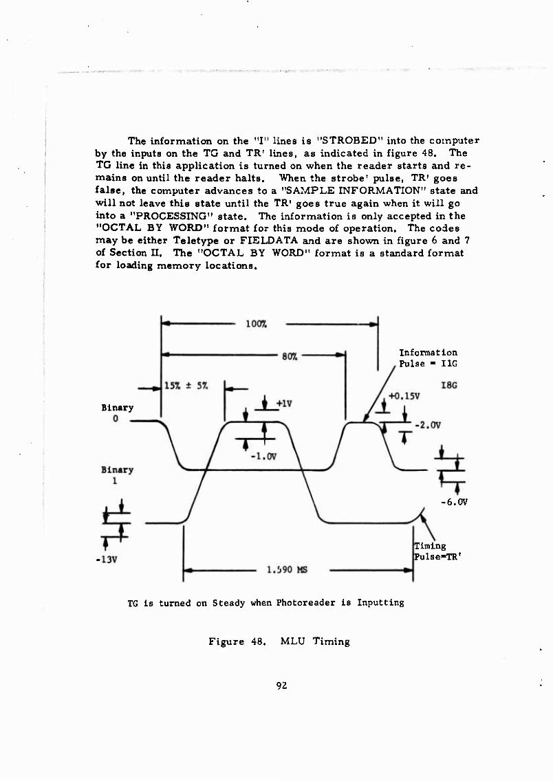
4wr u>w r«r'JO««'« ■ ■ .
The information on the "I" lines is "STROBED" into the computer by the inputs on the TG and TR1 lines, as indicated in figure 48. The TG line in this application is turned on when the reader starts and re- mains on until the reader halts. When the strobe' pulse, TR' goes false, the computer advances to a "SAMPLE INFORMATION" state and will not leave this state until the TR1 goes true again when it will go into a "PROCESSING" state. The information is only accepted in the "OCTAL BY WORD" format for this mode of operation. The codes may be either Teletype or FIELDATA and are shown in figure 6 and 7 of Section II. The "OCTAL BY WORD" format is a standard format for loading memory locations.
Information Pulse - I1G
Binary
6.0V
Timing Pulse-TR'
TG is turned on Steady when Photoreader is Inputting
Figure 48. MLU Timing
92
m
Separate individual characters can be used to put the computer into the "VERIFY", "FILL" or "HALT" modes. A "CLEAR" code is avail- able to clear any information inputted since the last "ENTER". When the compater is allowed to switch into the run mode from manual halt, by removing the -10 volts from GPRC and the +6 volts from GPHC, a "COMPUTE" code can be used for transferring to the instruction in the "I" register.
Whether the Teletype or FIELDATA code is to be interpreted de- pends on the CTTI input. With a -3 volts connected to CTTI, the Tele- type code applies. With CTTI left open, the FIELDATA code applies. The IFS input term determines the parity test to be performed, odd or even. In this instance the IFS is grounded to allow the FIELDATA paper-tape format to be accepted from the MLU.
The compater, after sampling the information, enters a "PRO- CESSING" state which in the Octal or BCD input modes can consume as high as 19 words times of 83 microseconds each or a total of 1577 microseconds. When finished "PROCESSING", the computer switches to a "WAIT FOR STROBE" state and remains there until TR', as de- scribed above, goes false again. The total "PROCESSING" time then determines the sampling rate, which for "WORST CASE" operation should be limited to 600 characters per second for Octal or BCD modes of Input.
When the computer switches to the Halt mode by reading a "HALT" code, being reset by the Reset Button, or generating a parity error on input, the "READER HALT" (RHO) output is energized thereby halting the reader. The MLU will stop within three characters.
The +35V is used to energize +35V1, +35V2, and +35V3 which energizes the appropriate write switches allowing the compater to write into "COLD STORAGE" and, therefore, all 8, 192 words of memory.
The Photo-Reader can also be used under program control. In this mode of operation, the computer remains in the "RUN" condition by leaving the GPRC and GPHC inputs open. The FBPR input can also be ignored since its application is only in the "HALT" condition. The compater can now by command (see programming manual) read in information in either Teletype or FIELDATA codes in the Octal, BCD,
93
or Alpha-numeric formats shown in figures 5, 6, and 7 of Section II. The information would still be read in synchronously at the Photoelec- tric Reader i ate and be strobed in the same manner as described above. However, when the computer is reading either Teletype or FIELDATA alpha-numeric codes, the "PROCESSING" time between strobes is re- duced to a maximum of 3 words at 83 usec/word. For satisfactory "WORST CASE" the maximum rate of input is then approximately 4000 characters/second. However, the MLU speed is limited to approxi- mately 600 cps.
The MRTT input is used for the mechanical reader on the control panel. When open, it allows the mechanical reader to read the Teletype code and when grounded, the FIELDATA code applies.
The manually initiated Fill mode is applicable to both the Keyboard and Mechanical Reader, and was described in Section III. B.
B. Digitronics Perforated Tape Reader
The Digitronics Model B3000 bidirectional perforated tape reader is designed to read 8 channel perforated tape at speeds up to 1000 charac ters per second, and is easily configured for FIELDATA compatibility. Figure 49 pictorially displays the Digitronics Tape Reader.
The Digitronics Tape Reader when functioning as a Memory Load- ing Unit (MLU) must be complemented by a unit that will provide control over the M18 computer and the tape reader.
Figure 50 indicates the cabling between J17 and the M18 compater, the tape reader and the unit providing control that is indicated as the SDR simulator. The connections and related terms between the various units is displayed in figure 51. A schematic presentation of the SDR simulator is shown in figure 52.
When functioning as an On-Line Bulk Storage Unit the Digitronics Reader may be caused to "READ" and "STOP" under the control of a computer stored program.
This can be accomplished by one of two signals. The RDYO term applied to the start circuitry of the Digitronics Tape Reader will step the reader character by character. Using the RGO term will permit
94
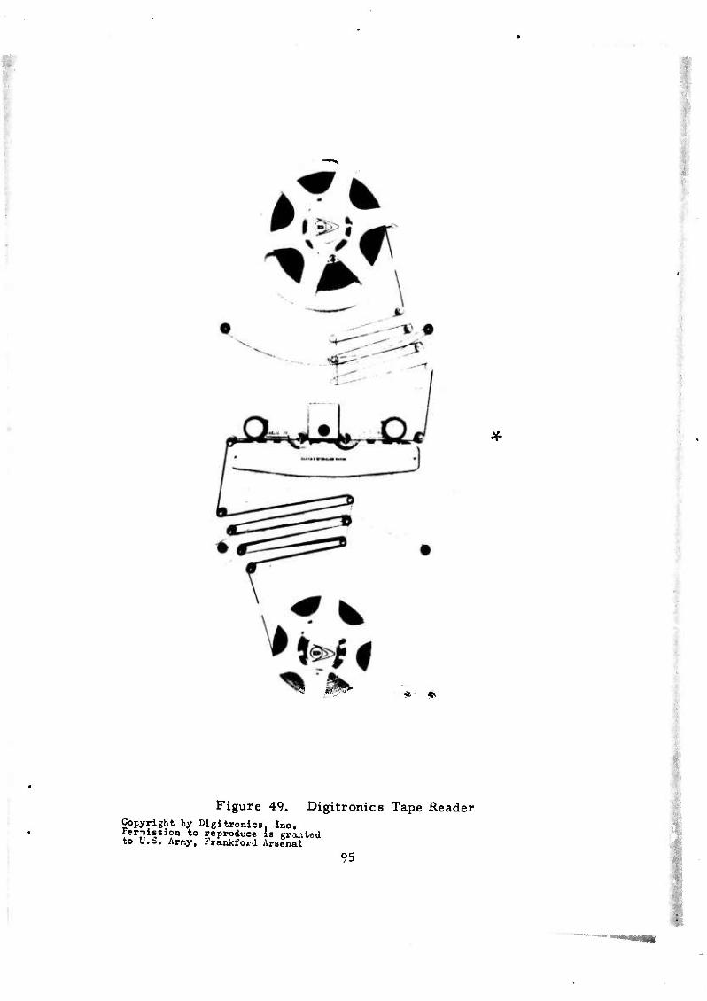
■
■
S5 ^"^ *> «
Figure 49. Digitronics Tape Reader Copyright by Digitronics, Inc. Permission to reproduce is granted to U.S. Army, Frankford Arsenal
95
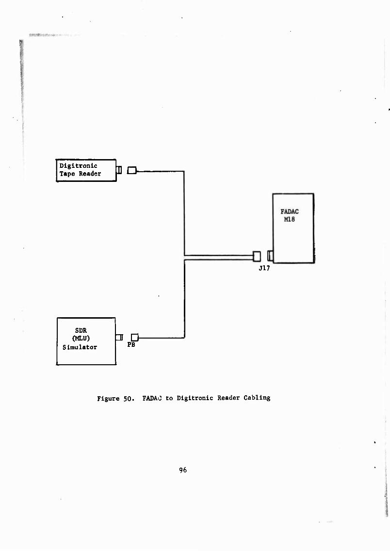
Dlgttronlc Tape Reader II 13-
SDR (MLU)
Simulator PB
J17
Figure 50. FADAO to Digitronic Reader Cabling
96
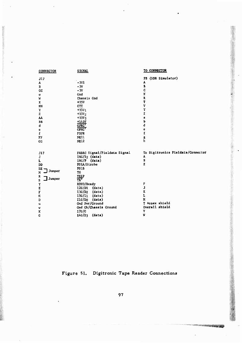
CONNECTOR
J17 A B cc u W X NN Y Z AA BB d e f FF GG
J17 J L DD EE M \\ Jumper
_J Jumper
SIGNAL TO CONNECTOR
PB (SDR Simulator)
-3V1 A -3V B -3V C Gnd N Chassis Gnd R +35V T CTT V +35V1 Y +35V2 Z +35V3 a +145V b GPRCr d GPHC7 e FBPR f NEU 8 NE12 h
FADAC Signal/Fieldata Signal To Dlgltronlcs Fleldata/Connector
I6G/I2 (data) A I8G/P (data) B PSIA/Strobe E PS IB TG TEIP TR'" RDYO/Ready r I2G/D1 (data) J I3G/D2 (data) K I5G/II (data) L I1G/D0 (data) M Gnd Pwr/Ground T +coax shield Gnd Ch/Chassls Ground Overall shield I7G/C V I4G/D3 (data) W
Figure 51, Digitronic Tape Reader Connections
97
•<
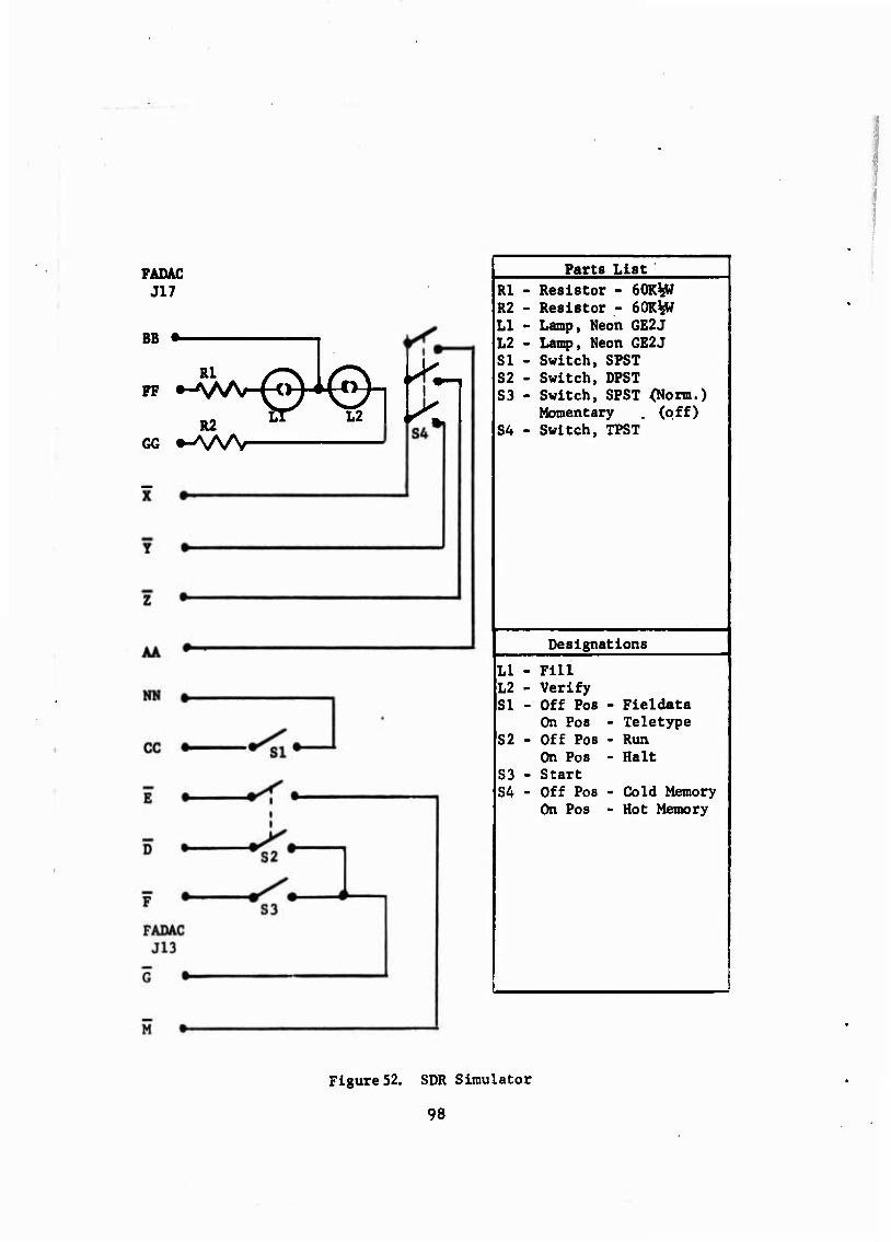
FADAC J17
BB *
"^^Vl >" R2
GG »-AAAr
f Parts List
Rl - Resistor - 60R^W R2 - Resistor - 60K^W LI - Lamp, Neon GE2J i L2 - Lamp, Neon GE2J [ SI - Switch, SPST S2 - Switch, DPST | S3 - Switch, SPST <Norm.) j
Momentary . (off) S4 - Switch, TPST i
j Designations
LI - Fill L2 - Verify SI - Off Pos - Fieldata
On Pos - Teletype | S2 - Off Pos - Run |
On Pos - Halt S3 - Start 1 34 - Off Pos - Cold Memory
!
On Pos - Hot Memory |
Figure 52. SDR Simulator
98
continuous reading at slew speed. lu order to be FADAC compatible the tape drive was modified so that slew speed would permit an accept- able character rate.
C. CTC Typewriter
A FIELDATA Page-Paper Tape Printer developed by Connecticut Technical Corporation, commonly referred to as the CTC Typewriter, has been operating as both an Input and an Output device with the M18 computer.
The CTC is a keyboard operated device with an integral FIELDATA compatible Paper Tape Reader and Perforator, capable of producing hard copy and transmitting to and receiving from FIELDATA lines using the FIELDATA alpha-numeric code. A functional block diagram of the FIELDATA printer is displayed in figure 53.
The integration of the CTC for inputting and outputting with the M18 are easily accomplished objectives. The CTC as an input trans- mitting device is connected to input connector J17 of the M18. Data is inputted on the eight "I" lines, RDYO is used as the controlling signal. An additional requirement is placed on this interface in that the timing signal from the CTC is the short duration FIELDATA strobe. The MIS internal PS1A pulse stretcher is utilized to condition this signal and effective interfacing is attained.
When the CTC is to function as a receiving device, it is connected to output connector J10 of the M18. The eight "D" lines transfer data to the CTC, STBO functions as the control. For complete compatibility with the MI8, the CTC ready signal requires inversion. Considering the proximity and availability of PS2, this pulse stretcher was employed. In this instance PS2 was used for the required inversion and not pri- marily for pulse expansion.
The CTC to M18 interface may be expanded and configured so as to allow the M18 to exercise additional control over the Input-Output operations.
An example of this, a method presently in use, is the utilization of the OPL lines to the CTC under computer program control.
99
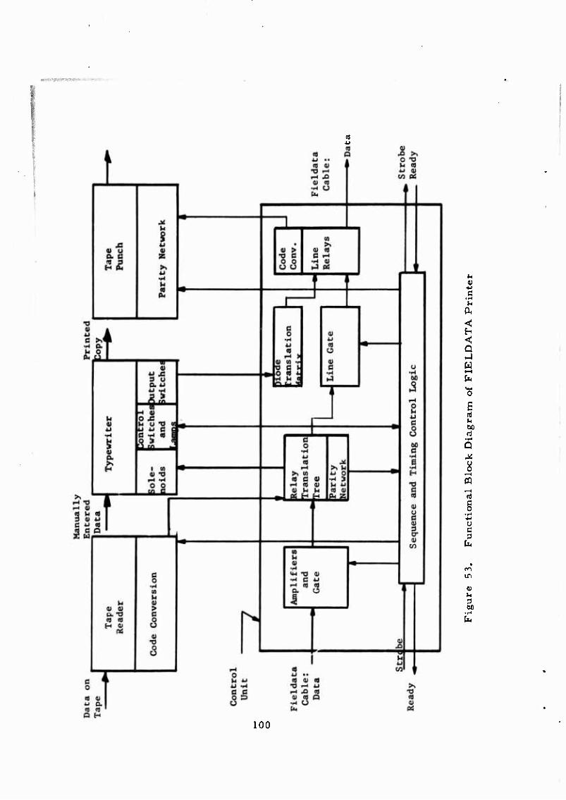
i>
c u
<
< Q -1 U
E
A: u o
CQ
§ ■r-" ■>->
u c
tn
(1) u
100
The CTC is connected to both the Input and Output connectors, J17 and J10. The OPL lines are connected in addition to the previously described data lines and control signals. The CTC is normally in the transmitting mode. When a predetermined OPL line goes true, under program control, this line causes the CTC to go the "RECEIVE" mode to accept data from the M18.
In order to be receptive to this external control signal, OPL, minor modification is required in the CTC.
D. Teletypewriter
A Teleprinter Corporation "Mite" teletypewriter has been em- ployed as an M18 computer output device.
The "Mite" has continuous duty speeds of 60, 75, 100, and 125 wpm based on the serial transmission of a five level baudot code. The change of speed is accomplished by the change of a "Mite" internal gear.
The M18 computer can two-wire serially output in one of two ways to the "Mite".
One method is the use of the MIS internal teletype oscillator that can be directed to an OPL line. This was described in Section IV, C. 2.d. This requires that the appropriate gear be installed in the "Mite" in order to be rate compatible.
A second and more often used method is to program the OPL lines and to use program delay techniques in order to provide the proper timing rate between the "Mite" and the MIS computer.
The "Mite" is pictorially displayed in figure 54, and is shown mounted in a special shockmounted case.
E. LP-2-150 Paper Tape Punch
A Model LP-2-150 Soroban perforator has proven to be an effec- tive output device for use with the Ml8 computer with appropriate LP2 modifications.
101
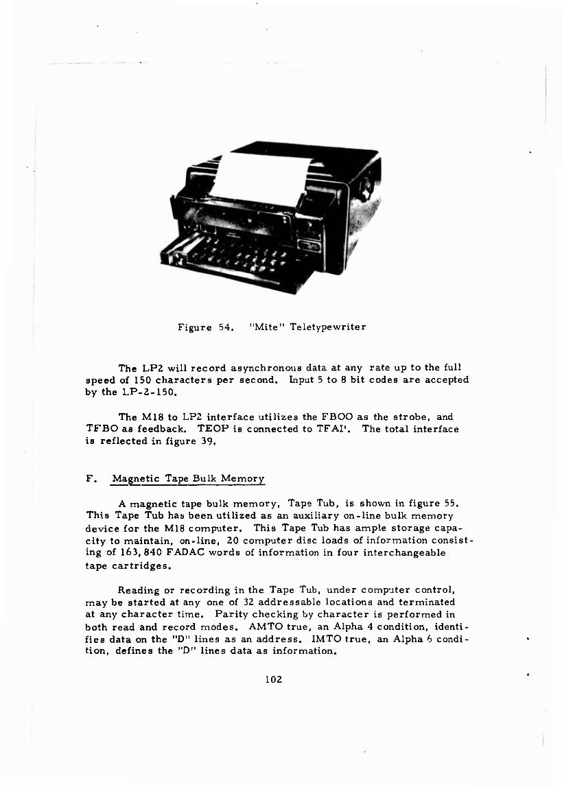
Figure 54. "Mite" Teletypewriter
The LP2 will record asynchronovis data at any rate up to the full speed of 150 characters per second. Input 5 to 8 bit codes are accepted by the LP-2-150.
The M18 to LP2 interface utilizes the FBOO as the strobe, and TFBO as feedback. TEOP is connected to TFAI'. The total interface is reflected in figure 39.
F. Magnetic Tape Bulk Memory
A magnetic tape bulk memory, Tape Tub, is shown in figure 55. This Tape Tub has been utilized as ein auxiliary on-line bulk memory device for the MIS computer. This Tape Tub has ample storage capa- city to maintain, on-line, 20 computer disc loads of information consist- ing of 163,840 FADAC words of information in four interchangeable tape cartridges.
Reading or recording in the Tape Tub, under computer control, may be started at any one of 32 addressable locations and terminated at any character time. Parity checking by character is performed in both read and record modes. AMTO true, an Alpha 4 condition, identi- fies data on the "D" lines as an address. IMTO true, an Alpha 6 condi- tion, defines the "D" lines data as information.
102
103
A presentation of FADAC-Tape Tub interfacing with pertinent logic terms is shown in figure 56.
G. FADAC to FADAC
To further indicate the input-output characteristics of the M18 computer, FADAC to FADAC data transferring can be accomplished by an appropriate interface.
This operation also offers alternatives in the application of strobes. One method, shown in figure 57, is a FADAC to FADAC communication link that utilizes the FADAC strobe signal. A second FADAC to FADAC interface configuration is illustrated in figure 58. In this second method the FIELDATA Ready-Strobe is employed and strobe signal conditioning by PSl and PS2 is required.
VI. SPECIALIZED APPLICATIONS
A. General
The previously emphasized inherent flexibility of the Input-Output capabilities of the MIS computer allow it to operate with a variety of peripheral equipment. Equipment of special design is easily adapted for connection to the MIS computer.
A number of system development programs have advocated the in- tegration of the Ml8 for their particular needs. These objectives in- cluded integrating multiple and varied kinds of peripheral devices with the M18 such that they operate in an asynchronous and multiplexed mode with respect to each other and with the M18.
The following examples relate to the technical approach for sys- tem integration to further delineate the inherent input-output flexibility of the M18.
104
FADAC
D100 D200
Tape Tirb
Information Lines
Information Transfer Address Transfer Strobe Feedback (Input), Strobe
(Output)
^Information Lines
Fill or Verify Feed'^ar <
Figure 56. FADAC - Tape Tub Interface
105
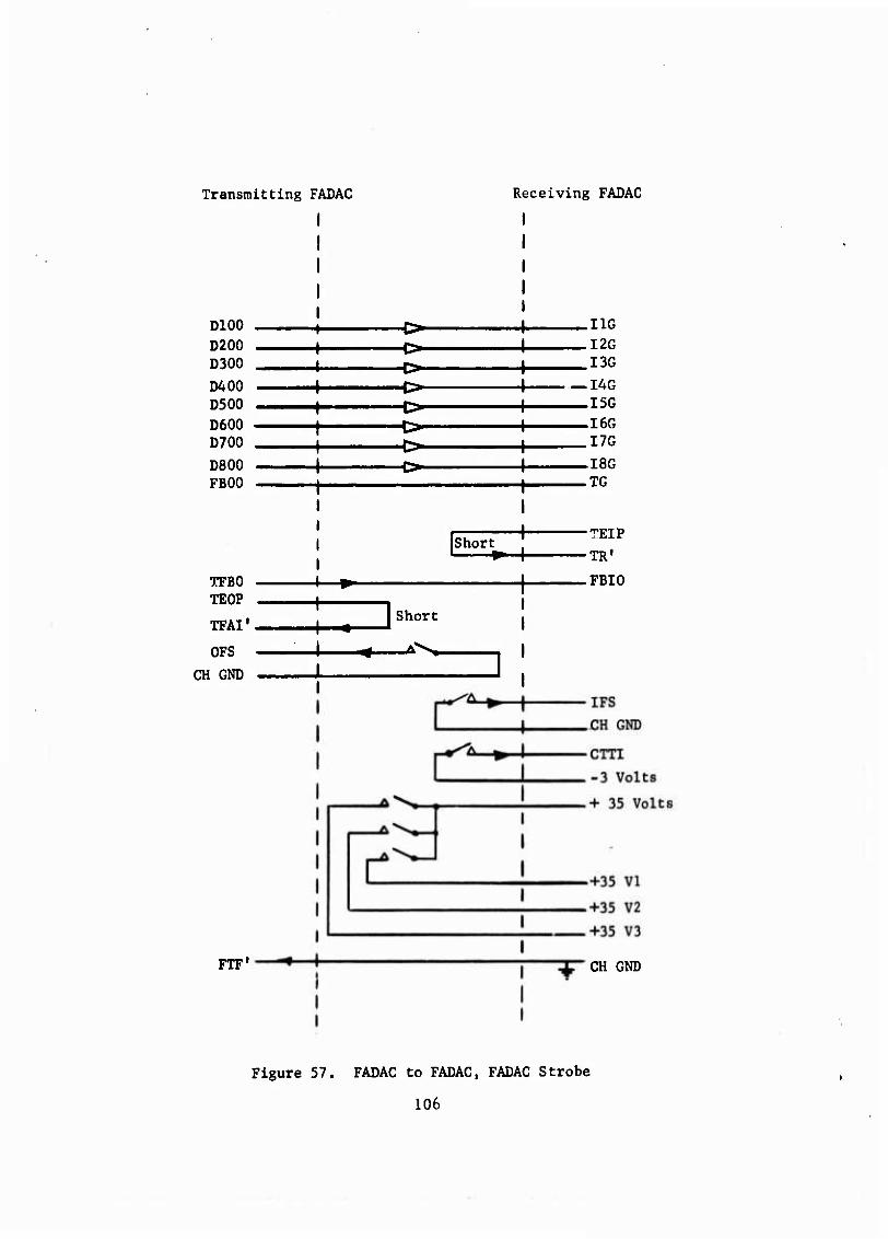
Transmitting FADAC Receiving FADAC
D100
D200 D300
D400 D500
D600 D700
D800 FBOO
TFBO TEOP
TFAI*
OFS
CH GND
Short
|Short
-4 Ä>>i-
FTF'
I1G
I2G I3G
— I4G I5G
I6G I7G
-I8G .TG
•TEIP
■TR'
.FBIO
CH GND
Figure 57. FADAC to FADAC, FADAC Strobe
106
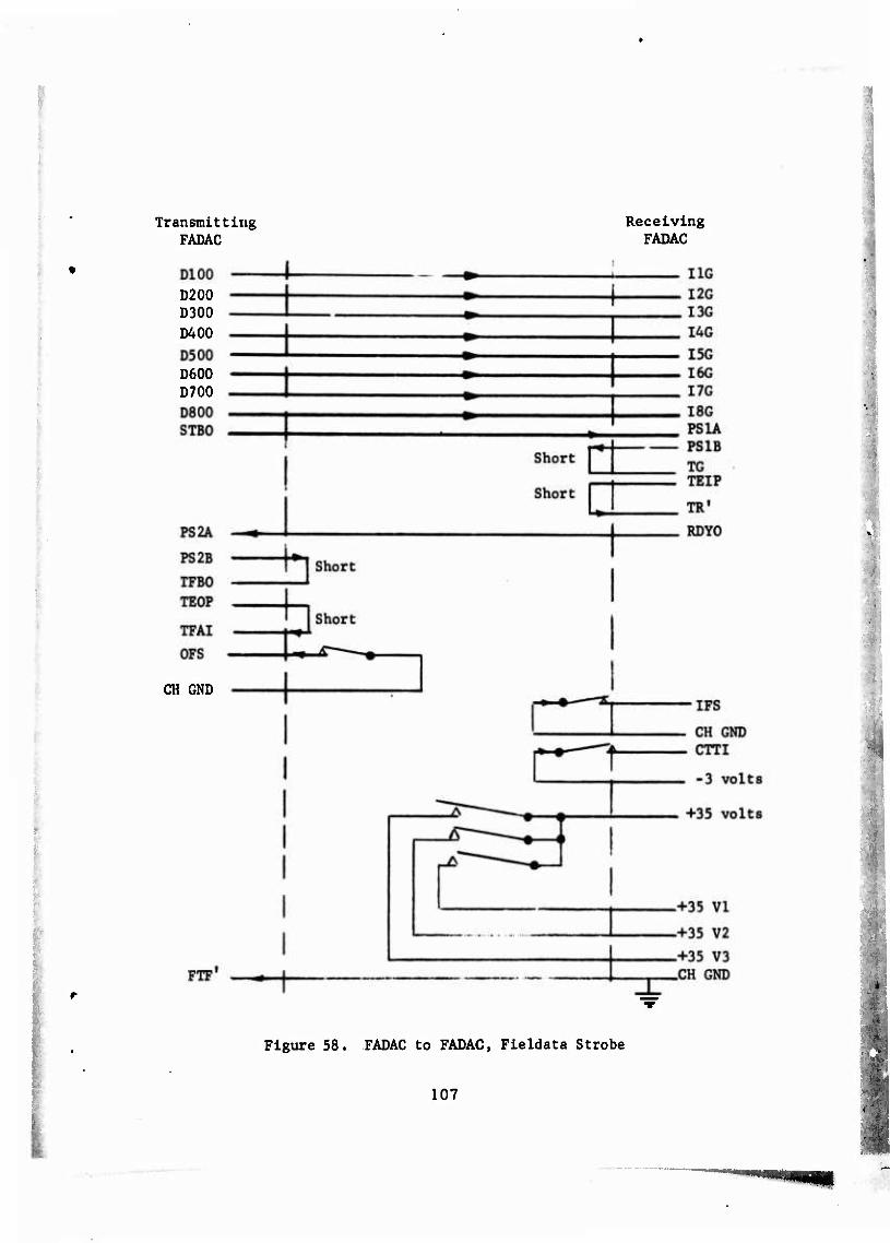
:
Transmitting FADAC
D200 D300
D400
Receiving FADAC
0600 D700
CH GND
Figure 58. FADAC to FADAC, Fieldata Strobe
107
B. Automatic Calibration-Laboratory Evaluation Unit (Auto-Cal)
The Auto-Cal is a development program to advance accuracy and flexibility at the Field calibration level.
This objective is to be accomplished by automatically calculating, through computer control, all electrical parameters in terms of three basic parameters - Voltage, Resistance, and Time.
By employing a series of indirect measurements, self-checks and cross calibrations, the equipment then becomes a self-contained self- calibrating measurement system which can also be used as a separate calibration device. Figure 59 is a block diagram of the Auto-Cal Sys- tems concept.
This developed equipment, in addition to employing conventional techniques, has incorporated devices to provide a high degree of tech- nical compliance to total input-output requirements.
1. Buffer-Trans later (BT)
A Buffer-Trans later (BT) is used to provide general commu- nication between the computer and the measurement system. The com- puter directs the BT to "make the connection", change the scale, initiate measurement cycle, etc.
Basically, the BT is a binary to decimal converter in that it accepts binary information in the form of eight (8) parallel bits at its input, decodes it and causes a change of state on one of its discrete out- put lines. Considering that there are 256 combinations in a set of eight (8) binary bits, the BT has 256 related discrete output lines. For con- venience, the output lines have been divided into sixteen (16) groups of sixteen (16) units each.
Functionally the computer by way of the Alpha-4 command will set up the eight bits on the Input lines of the BT, then issue a strobe signal. (The strobe signal indicates that data present on the output lines is to be acted upon.) Upon receipt of the strobe, the BT will decode the information, cause the addressed output line to change state and then generates a feedback signal to the compiter indicating that the requested action has taken place. Upon receipt of the feedback the process may be repeated.
108
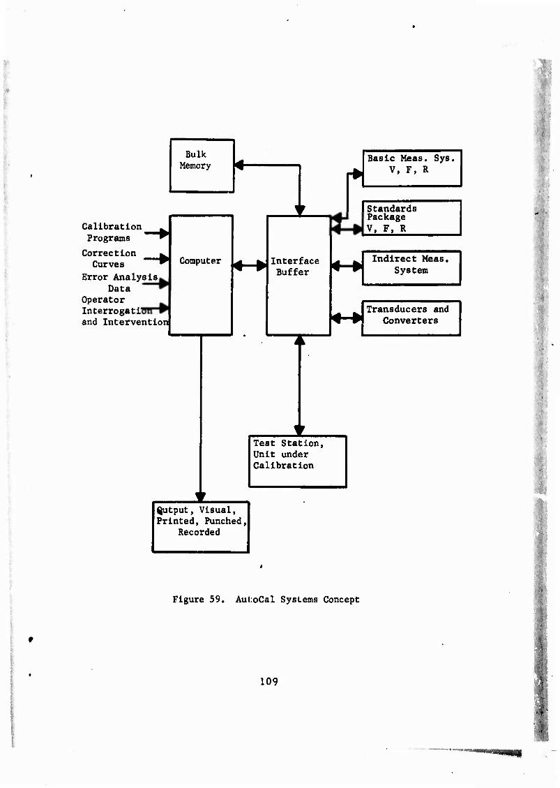
Bulk Memory
Calibration Programs
Correction Curves
Error Analysis Data
Operator Interrogate and Intervention
Computer Interface Buffer
Basic Meas. Sys, V, F, R
Standards Package
V. F, R
Indirect Meas. System
Transducers and Converters
Test Station, Unit under Calibration
$utput, Visual, Printed, Punched,
Recorded
Figure 59. Aul:oCal Systems Concept
109
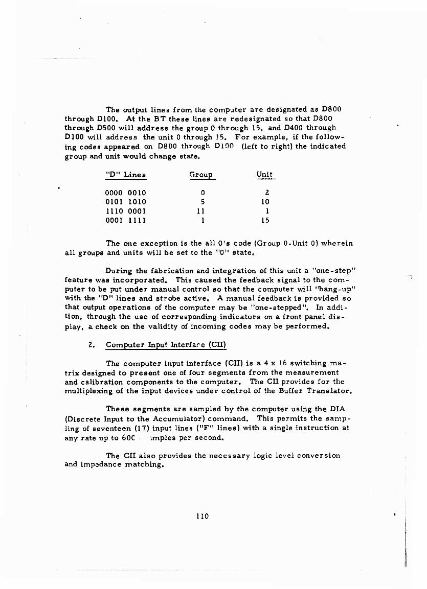
The output lines from the computer are designated as D800 through D100. At the BT these lines are redesignated so that D800 through D500 will address the group 0 through 15, and D400 through D100 will address the unit 0 through 15. For example, if the follow- ing codes appeared on D800 through D100 (left to right) the indicated group and unit would change state.
"D" Lines Group Unit
0000 0010 0 2 0101 1010 5 10 1110 0001 11 1 oooi mi i is
The one exception is the all O's code (Group 0-Unit 0) wherein all groups and units will be set to the "0" state.
During the fabrication and integration of this unit a "one-step" feature was incorporated. This caused the feedback signal to the com- puter to be put under manual control so that the computer will "hang-up" with the "D" lines and strobe active. A manual feedback is provided so that output operations of the computer may be "one-stepped". In addi- tion, through the use of corresponding indicators on a front panel dis- play, a check on the validity of incoming codes may be performed.
2. Computer Input Interface (CII)
The computer input interface (CII) is a 4 x 16 switching ma- trix designed to present one of four segments from the measurement and calibration components to the computer. The CII provides for the multiplexing of the input devices under control of the Buffer Translator.
These segments are sampled by the computer using the DIA (Discrete Input to the Accumulator) command. This permits the samp- ling of seventeen (17) input lines ("F" lines) with a single instruction at any rate up to 60C imples per second.
The CII also provides the necessary logic level conversion and impedance matching.
"1
110
3. Remote Program Addressing
The Remote Program Addressing is accomplished by switch- ing hardware physically external to the computer, but functionally in
* parallel with the Ml8 front panel Matrix. This permits a degree of con- trol over the computer from some remote location. Figure 60 schema- tically shows the front panel switching that characterizes the Remote Program Addressing operation.
These switches are mounted on the Auto-Cal Console control panel and labeled with the appropriate operation to be performed.
Depressing one of these encoding switches will generate a combination of signals that are applied to the M18 "F" lines. An im- portant characteristic of these switches is that there is a mechanical delay in the closure of the segment that provides the strobe signal to the computer. This insures that the switch combination closures are firm before strobing into the MIS. The delayed strobe activates the ESU term.
The ESU term in turn transfers computer control to the "RECEIVE" memory location which contains an input program to sample the "F" lines. The input program samples the "F" lines into the "A" register by a DIA command and then shifts these "F" lines contents in "A" to the bit positions normally influenced by the Sample Matrix switches.
The Remote Program Addressing function is then interpreted by the computer in essentially the same manner as a Matrix operation.
As an example of reconfiguring, duplicate "COMPUTER RESET" buttons are employed to generate the EER term, so that from two different locations this control function can be exercised.
The number of information and control lines between the various portions of the Auto-Cal system is displayed in figure 61.
C. MAIDS MARK III
The MAIDS MARK III is a development program to provide a sys- tem of test equipment for accurately diagnosing Tank-Automotive ma- terial. This system functions in an automatic mode and removes from
111
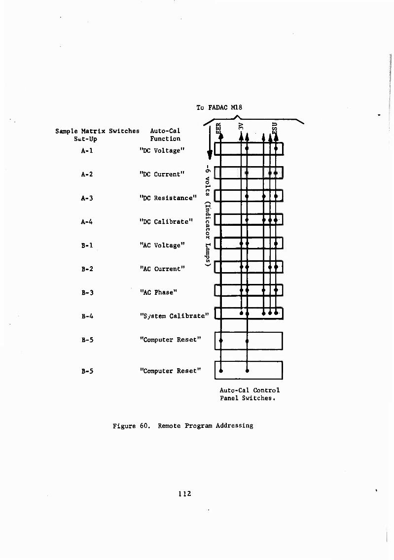
To FADAC Ml8
Sample Matrix Switches Auto-Cal Sttt-Up
u
A-l
A-2
A-3
A-4
B-l
B-2
B-3
B-4
B-5
B-5
Function
"DC Voltage"
"DC Current"
"DC Resistance"
■
3' a
"DC Calibrate" o
o i-i
"AC Voltage"
"AC Current"
"AC Phase"
"System Calibrate"
"Computer Reset"
"Computer Reset"
> 1 | ||' A p T 1 T El T T 1 fa
4 f 1 r T p T T 1 T p
| • T T 1 p 1 ^ i im
fa
1 1 *
1 I I Auto-Cal Control Panel Switches.
"S.
Figure 60. Remote Program Addressing
112
Remote Program Addressing
J101 Buffer
Translator (B-T)
(4)
(1)
J10 Computer J17
(27 (16)
X5T 1 Computer Input
Interface (CII)
(32)
(1)
Counter
( ) = No. of Information Or Control Lines
Figure 61. Auto-Cal Information and Control Lines
me*
■
113
f ■' '■' ■■
the diagnosis many judgment factors which of necessity depend on highly skilled personnel.
From a functional viewpoint, the MAIDS MARK III system is divided into four major subsystems and a functional block diagram is shown in figure 62.
The M18 is employed as the computer controller subsystem. The following description is directed to the M18 interface considerations and related peripheral equipment.
I. Input-Output Buffer (IOB)
The Input-Output Buffer (IOB) enables an M18 computer to con- trol a variable and flexible number of external selection modules provides up to 24 sets of form "C" relay contacts for switching. The IOB operates in conjunction with a stored program in the Ml8 to provide a coordination center for control and information transfer to and from the various ex- ternal modules by FADAC.
In this particular application, MAIDS MARK III, the IOB con- nects a FADAC to a bulk storage unit (Magnetic tape), a printer and to a vast number of display, measurement, stimuli, and switching devices. This system is shown in a simplified form in figure 63. In this instance the FAJDAC to IOB interface is divided into four different categories based on signal destination. They are the IOB control signals, Tape Tub sig- nals, Measurements Inputs, and Teletype signals, as described below:
a. IOB Control Signals
The operations to be configured by the IOB are deter- mined by 24 programming bits and ein 8 bit external module address supplied by FADAC. This data is supplied by FADAC, via an "alpha- numeric 6 by word output", and transferred to the IOB coincident with a discrete output line, OPL4.
In practice a sequence of OPL commands are employed. Initially a DOF is used to clear the OPL lines. Following this an OPL5 is used essentially as a reset signal to the IOB in the event that there is an error remaining from a previous operation. Then the OPL4, in con- junction with the alpha-numeric characters is used to set up the impend- ing operation.
114
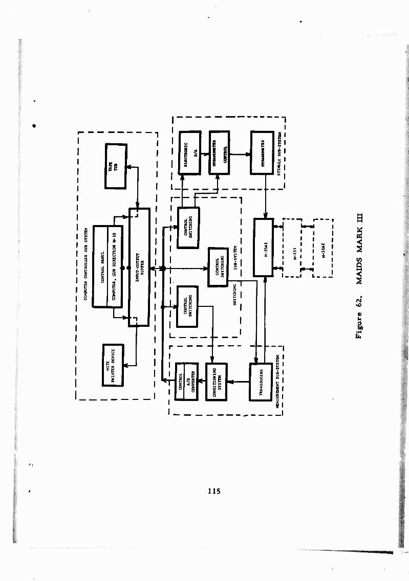
u
H li
S ^ ä ^
rj:—~
' -J J < >
Si 3 ■ I I 6 I
I
11 P V) S 5)
H J—
i i
Ml
L :
"I
fl $1 _l
115
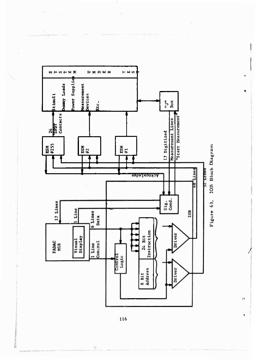
Vl >< (A H U S S SB Q U « H W w i
I a 3
W
0)
o
c v 5 (A h ai 3 it ID i-l «0 >
JL£. u 4 4J B O
fco o
CM Ö
JL
= X •-> o : pa
J2 r TF n^ 0) N
60
Q
aapa^AOu^ov
w
£• T c ^^tai 0
4J -i-t
4-* •i-l 4J PQ O 1 ^ ^^^^ ** ■• CM J fc-«^^ o 1
c w 1
10 "
4-i c 1 •rt 1» pa ^
^ oo <; 1
£ rt u m ti
■6 X u o
CQ
CQ O
|1
116
I
b. Tape Tub Signals
The T.npe Tub functions under the control of OP LI and OPL2. The OPL1 is primarily a tape turn-on signal as well as defining the information on the "D" lines for cartridge and track selection.
OPL2 indicates information on the "D" lines that deter- mine whether a read or write operation is to be performed and further provides the block address.
The efficiency of the Taps Tub-to-FADAC data transfer operation was improved by the use of the CTTI signal term.
In a normal mode of data transferring the Taps Tub per- forms a parity test that is done redundantly by the FAD AC. Upon a par- ity error generation, the Tape Tub will provide an indication (F251 True) whereas the FADAC will indicate an error and Halts.
As indicated in Section IV, Table II, the CTTI term will prohibit parity testing by FADAC when in a "RUN" mode. Therefore, by employing the CTTI term, parity tests of transferred data will still be performed, by the Tape Tub, but the computer operations are not halted.
In this manner a transient parity error can be overcome by a repeat cycle of data transferring without halting operations.
Repetitive parity test failures after several cycles indi- cates a firmly established error condition requiring remedial action.
c. Measurement Signals
All measurement inputs to the M18 will be entered as a set of 17 bits over 17 discrete inputs available on the FADAC Input- Output connectors, J17 and J10.
F30 can only be used when a "START MEASUREMENT" signal is being transmitted, since it is time shared with the IOB,
The significance of these 17 discrete inputs will vary from time to time, according to which of the measurement devices have been energized by the selection process. Furthermore, the selected
V 117
*:»
measurement device will not transmit any return signals until after it receives a "START MEASUREMENT" command from the IOB. Prior to this time, the "ERROR" signal that is generated within the IOB is the only signal connected to any of the discrete input lines. This en- ables the FADAC program to sample and "RESET" the "ERROR" signal ^ after all the module programming has been completed and to insure proper set-up conditions before issuing the "MEASURE" discrete output command.
d. Teletype Signals
OPL3 is used for teletype output of data.
2. Computer Measurement Turing
Transducers are an integral part of the MAIDS MARK III system and their generated signals require Analog to Digital conver- sion for computer processing.
A common multiplexed "A" to "D" converter is employed and is under FADAC control. As an indication of real time control a TOA', M18 available output term, when "AND" gated with OPL6 can be used to trigger the transfer of measurements from the "A" to "D" converter to the computer.
TOA1 is internally synchronized and is available at the end of each FADAC word. In order to input data to the M18 at least two word times are required; optimized as a DIA command followed by a store in memory command. By toggling a complementing Flip-Flop with TOA1 the developed Flip-Flop signal is then in synchronism with FADAC at a two word rate.
This Flip-Flop developed signal available every two word times is then used as a "START MEASURE" signal under control of OPL6. This operation permits the maximum transfer rate of data to the computer at a known fixed time.
3. External Device Integration
In the primary FADAC concept specific "F" lines were used initially as identification lines. These lines served to indicate to the computer what specific devices were connected and on-line under pro- '* gram control.
118 ^
.
As more devices become available for MI8 computer adapta- tion, greater care must be taken when integrating a number of these components into a system configuration.
A case in point is that the MLU applies a "PRESENT" signal to F30. The IOB also utilizes F30 as a return "ERROR" signal to FADAC. If precautions were not taken when using both the MLU and the JOB an ambiguous condition would arise. Merely the presence of the MLU with its "PRESENT" signal applied to F30 could be erroneously interpreted as an IOB "ERROR" signal that is also applied to F30.
119
DOCUMENTATION T ,18TING 4?
TM9-1220-22I- Computer, Gun Direction, M18
1
10 Operators Manual 20/1 Organization Maintenance Manual 20/2 Composite Test Program Printout 34/1 Field Maintenance Manual 34/6 Wire List (Terms) 34/7 Wire List (Components) 50 Depot Maintenance Manual
9
TM9-1290.326- Reproducer, Signal Data AN/GSQ-64
12 Operators and Organizational Maintenance Manual 35 Field and Depot Maintenance Manual
Notes on Development Type Material
FCDD-361 Volume IV Revised - Programming Manual
Memorandum Report
M66-5-1 Automatic Test Equipment, MAIDS MARK III AMCMS Code 4440. 25. 0029
Technical Study of the Army Calibration Program OMS 2340. 1470000.01
Final Engineering Report
Magnetic Tape Memory System Contract DA-04.495-AMC-23(X) Phase I
Input Output Buffer, System Desc. Vol 1 Contract DA-36.038-AMC-1175(A)
\
120 \
MMHHBRMS
DOCUMENTATION LISTING (Coat'd)
Final Engineering Report (Cont'd)
Paper Tape-Page Printer, Instruction Manual Reference Spec. TR-AD.20-62 Contract OA.36-039-0096l(E)
Paper Tape Reader Section of the Fieldata Systems Design Reference Notebook USAEPG Contract No. DA.36-039-AMC-00954(Y)
121
I

'■' r Unclassified
Stcuritr a«««lflc«tion
DOCUMENT CONTROL DATA .R&D (Uturttr •t—IHemtton ol Uli», boär •! abattmel mnd InltMhtg mmolmilan mual f itlwtd wh*> Of omr»ll f port I» elaitHM)
ONI«INATIN« ACTIVITY (Coiporml* author) FIRE CONTROL DEVELOPMENT AND ENGINEERING FRANKFORD ARSENAL Philadelphia, Pa. 19137 - ATTN:
LABS. SMUFA.L3300
1«. HKPONT ■BCURITV CLAMIFICATION
Unclassified 16. anou^
•■ mmmomr TITLK
COMPUTER, GUN DIRECTION M18 (FADAC) APPLICATIONS MANUAL
l (Trp* ol fpott anrf Jnafmir* dal«.;
t- AUTMONW) (FUutm—m, mum* tntUmt. Imalnam»)
PRICE, Thomas J,
•■ mrmonr OATI
May 1967 121 •a. CON M. ONiaiNATOR*« NBFORT NUMaCRItl
AMCMS Code 4410. 15.8001 b. pmejKcr HP. TN-1119
OTHER RKRQRT NO(tl (Any oA« Mia nport)
numburm Mal «Mir *• mitlgrutd
10. DISTRIBUTION tTATEMCNT
Distribution of this document is unlimited.
It. iPONtORma MILITARY ACTIVITY
U. S. Army Weapons Command
nTABSTRAlt
//. This FADAC Applications Manual is a summary document which provides informa tion required by system engineers for integrating the MIS (FADAC) with peripheral devices and equipment.
Brief introductory descriptions of the MIS characteristics and command structure are provided; whereas the input-output capabilities are discussed in detail and re- lated logic terms are fully defined.
Descriptions of Interfacing with representative input-output devices are provided to indicate the M18 input-output operations. A brief discussion of system develop- ment programs that utilize the MIS are also provided, as examples, to further deli- neate the inherent input-output flexibility of the MIS for systems integration.
ff^ff\ POm 4 A TO RBRI-Acca oo FORM UT«. I DDIMOVM|4/W OO»OI.«T« row ARMY U«.
JAN M. WMICM IS
Unclassified Security ClaaalficaMon
Unclassitied S«curtty CU»»lfic«tton
K«V WORD! LINK A
NOLI WT
LINK ■ LINK C
ROLK NOLB
Computer - FADAC Input and Output Devices Auxiliary Memory FADAC Command Instruction
Unclassified tocorlty Claulftcati««