Embed Size (px)
Citation preview
Thin Solid Films 520 (2012) 2656–2662
Contents lists available at SciVerse ScienceDirect
Thin Solid Films
j ourna l homepage: www.e lsev ie r .com/ locate / ts f
Hydrothermal treatment of ZnO nanostructures
Xinyi Chen a, Alan Man Ching Ng a, Aleksandra B. Djurišić a,⁎, Chi Chung Ling a, Wai Kin Chan b
a Department of Physics, The University of Hong Kong, Pokfulam Road, Hong Kongb Department of Chemistry, The University of Hong Kong, Pokfulam Road, Hong Kong
⁎ Corresponding author. Tel.: +852 2859 7946; fax:E-mail address: [email protected] (A.B. Djurišić).
0040-6090/$ – see front matter © 2011 Elsevier B.V. Alldoi:10.1016/j.tsf.2011.11.019
a b s t r a c t
a r t i c l e i n f oArticle history:Received 13 June 2011Received in revised form 17 October 2011Accepted 4 November 2011Available online 13 November 2011
Keywords:OxidesN-nanorodsZinc oxideHydrothermal treatmentsScanning electron microscopyMorphologyPhotoluminsescence
Hydrothermal treatment of ZnO nanostructures involves low temperatures (150–200 °C) and elevated watervapor pressure for the purpose of the improvement in the material properties. Under such moderate conditions,no significant changes in themorphologywould be expected. Nevertheless, such treatment results in a significantchange of nanostructured morphologies of ZnO. The observed changes are dependent on the starting materialproperties and the substrate used for the growth. In the case of Si substrate, hydrothermal treatment results insignificant Si contamination of the samples. In terms of the optical properties, improvements are observed onlyin some cases, while samples with excellent starting optical properties are degraded by the treatment. Mecha-nisms responsible for the observed changes are discussed.
© 2011 Elsevier B.V. All rights reserved.
1. Introduction
ZnO is a wide band gap semiconductor which is of interest for avariety of optoelectronic device applications [1–3]. It can be grownby a variety of different methods in a number of different nanostruc-tured morphologies [1,2]. Among these methods, solution-basedgrowth of ZnO is of significant interest due to its simplicity and lowcost [1,2]. However, the crystal quality and consequently the opticalquality of solution-grown samples is often inferior [1,2], although itcan be improved by post-growth treatment such as annealing [2]and hydrothermal treatment [4,5]. Hydrothermal treatment [4–6]has been proposed as a simple and efficient way to improve theproperties of ZnO by a mild and relatively low temperature procedure(150 °C [4,5] or 200 °C [6]). It has been shown that such treatmentimproves the crystallinity of ZnO, as well as the intensity of the UVphotoluminescence (PL), while visible emission was quenched [4].The observed improvements were attributed to local ZnO recrystalli-zation and improvement in surface quality due to reactions betweenwater vapor and various surface defects [4]. Hydrothermal treatmentwas also reported to result in the improved solar cell [5] and gassensor [6] performance.
It has been proposed that if the sample is in direct contact withwater during hydrothermal treatment, morphology changes will occurwhile this is not the case if the sample is placed above thewater surfacelevel [4]. However, morphology changes have also been observed for
+852 2559 9152.
rights reserved.
hydrothermal treatment at higher temperature (200 °C) [6]. In addition,it has been recently reported that ZnO nanocrystals in powder form ex-hibit growth in ambient environment which is affected by the vaporpressure of water [7]. In all cases, the involvement of native defects inthe process has been proposed [4,6,7]. Therefore, we have investigatedthe influence of hydrothermal (HT) treatment on the ZnO nanostruc-tures with different morphologies and different native defect typesand concentrations.
2. Experimental section
2.1. Materials preparation
Tetrapods have been grown according to a previously describedprocedure [8] and Si was used as a substrate for the growth. We haveseparated tetrapods which exhibit no defect emission (M zone) andtetrapods which exhibited green defect emission (H zone) based ongrowth temperature andoptical properties and subjected them tohydro-thermal treatment. In addition to tetrapods, we have prepared ZnOnanorods by vapor deposition [9] (VD rods) and hydrothermal growth(HT rods) [10]. To further study the effect of morphology, ZnO filmshave been prepared by e-beam evaporation using AST PEVA 400 ES. Toinvestigate the influence of substrate used, nanostructures were grownon Si (100) and α-sapphire (001). For hydrothermal treatment, thesamples were placed in a 65 ml autoclave filled with 15 ml of water,3 cm above the water surface. Then the autoclave was sealed and placedin an oven and the treatment was performed at 150 °C for 12 h. All thesampleswere subjected to the same hydrothermal treatment conditions.
2657X. Chen et al. / Thin Solid Films 520 (2012) 2656–2662
2.2. Materials characterization
The morphology of the samples was examined by scanningelectron microscopy (SEM) using a JEOL JSM-7001 F SEM (at 15 kV),while photoluminescence (PL) spectra were measured using a HeCdlaser (325 nm) and a PDA-512_USB (Control Development Inc) fiber-optic spectrometer. Transmission electron microscopy (TEM), energydispersive X-ray spectroscopy (EDX), and selected area electrondiffraction (SAED) were performed using Philips Tecnai G2 20 S-TWIN (at 200 kV). X-ray diffraction (XRD) measurements wereperformed using a Bruker AXS SMART CCD diffractometer (Cu source,wavelength 1.54178 Å, locked coupled mode).
3. Results and discussion
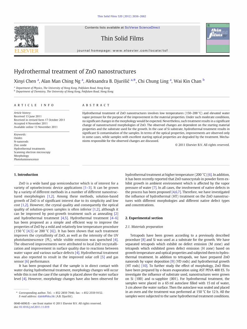
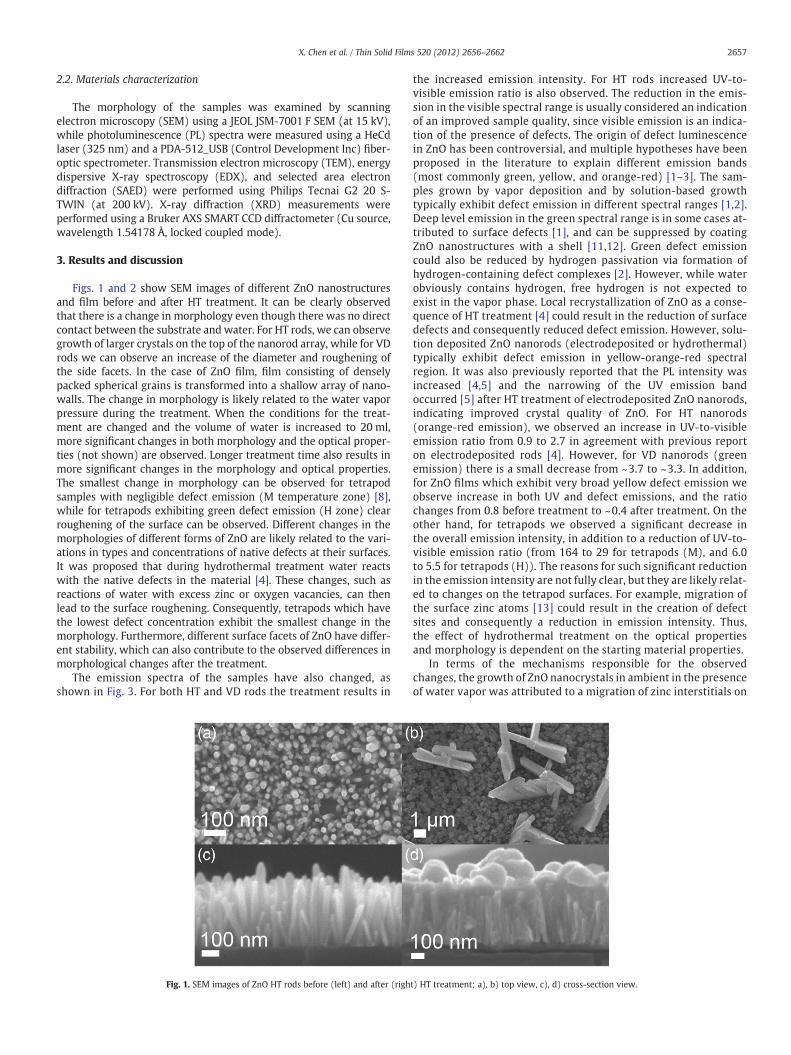
Figs. 1 and 2 show SEM images of different ZnO nanostructuresand film before and after HT treatment. It can be clearly observedthat there is a change in morphology even though there was no directcontact between the substrate and water. For HT rods, we can observegrowth of larger crystals on the top of the nanorod array, while for VDrods we can observe an increase of the diameter and roughening ofthe side facets. In the case of ZnO film, film consisting of denselypacked spherical grains is transformed into a shallow array of nano-walls. The change in morphology is likely related to the water vaporpressure during the treatment. When the conditions for the treat-ment are changed and the volume of water is increased to 20 ml,more significant changes in both morphology and the optical proper-ties (not shown) are observed. Longer treatment time also results inmore significant changes in the morphology and optical properties.The smallest change in morphology can be observed for tetrapodsamples with negligible defect emission (M temperature zone) [8],while for tetrapods exhibiting green defect emission (H zone) clearroughening of the surface can be observed. Different changes in themorphologies of different forms of ZnO are likely related to the vari-ations in types and concentrations of native defects at their surfaces.It was proposed that during hydrothermal treatment water reactswith the native defects in the material [4]. These changes, such asreactions of water with excess zinc or oxygen vacancies, can thenlead to the surface roughening. Consequently, tetrapods which havethe lowest defect concentration exhibit the smallest change in themorphology. Furthermore, different surface facets of ZnO have differ-ent stability, which can also contribute to the observed differences inmorphological changes after the treatment.
The emission spectra of the samples have also changed, asshown in Fig. 3. For both HT and VD rods the treatment results in
Fig. 1. SEM images of ZnO HT rods before (left) and after (righ
the increased emission intensity. For HT rods increased UV-to-visible emission ratio is also observed. The reduction in the emis-sion in the visible spectral range is usually considered an indicationof an improved sample quality, since visible emission is an indica-tion of the presence of defects. The origin of defect luminescencein ZnO has been controversial, and multiple hypotheses have beenproposed in the literature to explain different emission bands(most commonly green, yellow, and orange-red) [1–3]. The sam-ples grown by vapor deposition and by solution-based growthtypically exhibit defect emission in different spectral ranges [1,2].Deep level emission in the green spectral range is in some cases at-tributed to surface defects [1], and can be suppressed by coatingZnO nanostructures with a shell [11,12]. Green defect emissioncould also be reduced by hydrogen passivation via formation ofhydrogen-containing defect complexes [2]. However, while waterobviously contains hydrogen, free hydrogen is not expected toexist in the vapor phase. Local recrystallization of ZnO as a conse-quence of HT treatment [4] could result in the reduction of surfacedefects and consequently reduced defect emission. However, solu-tion deposited ZnO nanorods (electrodeposited or hydrothermal)typically exhibit defect emission in yellow-orange-red spectralregion. It was also previously reported that the PL intensity wasincreased [4,5] and the narrowing of the UV emission bandoccurred [5] after HT treatment of electrodeposited ZnO nanorods,indicating improved crystal quality of ZnO. For HT nanorods(orange-red emission), we observed an increase in UV-to-visibleemission ratio from 0.9 to 2.7 in agreement with previous reporton electrodeposited rods [4]. However, for VD nanorods (greenemission) there is a small decrease from ~3.7 to ~3.3. In addition,for ZnO films which exhibit very broad yellow defect emission weobserve increase in both UV and defect emissions, and the ratiochanges from 0.8 before treatment to ~0.4 after treatment. On theother hand, for tetrapods we observed a significant decrease inthe overall emission intensity, in addition to a reduction of UV-to-visible emission ratio (from 164 to 29 for tetrapods (M), and 6.0to 5.5 for tetrapods (H)). The reasons for such significant reductionin the emission intensity are not fully clear, but they are likely relat-ed to changes on the tetrapod surfaces. For example, migration ofthe surface zinc atoms [13] could result in the creation of defectsites and consequently a reduction in emission intensity. Thus,the effect of hydrothermal treatment on the optical propertiesand morphology is dependent on the starting material properties.
In terms of the mechanisms responsible for the observedchanges, the growth of ZnO nanocrystals in ambient in the presenceof water vapor was attributed to a migration of zinc interstitials on
t) HT treatment; a), b) top view, c), d) cross-section view.
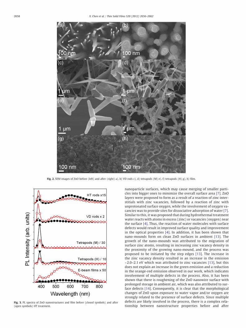
Fig. 2. SEM images of ZnO before (left) and after (right) a), b) VD rods c), d) tetrapods (M) e), f) tetrapods (H) g), h) film.
Fig. 3. PL spectra of ZnO nanostructures and film before (closed symbols) and after(open symbols) HT treatment.
2658 X. Chen et al. / Thin Solid Films 520 (2012) 2656–2662
nanoparticle surfaces, which may cause merging of smaller parti-cles into bigger ones to minimize the overall surface area [7]. ZnOlayers were proposed to form as a result of a reaction of zinc inter-stitials with zinc vacancies, followed by a reaction of zinc withunprotonated surface oxygen, while the involvement of oxygen va-cancies was to provide sites for dissociative adsorption of water [7].Similar to this, it was proposed that during hydrothermal treatmentwater reacts with atoms in excess (zinc) or vacancies (oxygen) nearthe surface [4]. Thus, the reaction of water molecules with surfacedefects would result in improved surface quality and improvementin the optical properties [4]. In addition, it has been shown thatnano-mounds form on clean ZnO surfaces in ambient [13]. Thegrowth of the nano-mounds was attributed to the migration ofsurface zinc atoms, resulting in increasing zinc vacancy density inthe proximity of the growing nano-mound, and the process wasproposed to be initiated by the step edges [13]. The increase inthe zinc vacancy density resulted in an increase in the emission~2.0–2.1 eV which was attributed to zinc vacancies [13], but thisdoes not explain an increase in the green emission and a reductionin the orange-red emission observed in our work, which indicatesinvolvement of multiple defects in the process. Also, it has beenshown that there is roughening of the ZnO nanowire surface withprolonged storage in ambient air, which was also attributed to sur-face defects [14]. Consequently, it is clear that the morphologicalchanges of ZnO upon exposure to water vapor and/or oxygen arestrongly related to the presence of surface defects. Since multipledefects are likely involved in the process, there is a complex rela-tionship between nanostructure properties before and after
2659X. Chen et al. / Thin Solid Films 520 (2012) 2656–2662
treatment. The structures with low defect densities, such as tetra-pods (M), will not exhibit significant morphological changes andno improvement in the optical properties. For other nanostruc-tures, the effect of the treatment will depend on the startingmaterial properties.
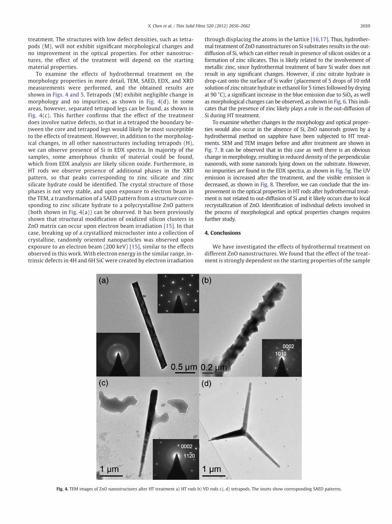
To examine the effects of hydrothermal treatment on themorphology properties in more detail, TEM, SAED, EDX, and XRDmeasurements were performed, and the obtained results areshown in Figs. 4 and 5. Tetrapods (M) exhibit negligible change inmorphology and no impurities, as shown in Fig. 4(d). In someareas, however, separated tetrapod legs can be found, as shown inFig. 4(c). This further confirms that the effect of the treatmentdoes involve native defects, so that in a tetrapod the boundary be-tween the core and tetrapod legs would likely be most susceptibleto the effects of treatment. However, in addition to the morpholog-ical changes, in all other nanostructures including tetrapods (H),we can observe presence of Si in EDX spectra. In majority of thesamples, some amorphous chunks of material could be found,which from EDX analysis are likely silicon oxide. Furthermore, inHT rods we observe presence of additional phases in the XRDpattern, so that peaks corresponding to zinc silicate and zincsilicate hydrate could be identified. The crystal structure of thosephases is not very stable, and upon exposure to electron beam inthe TEM, a transformation of a SAED pattern from a structure corre-sponding to zinc silicate hydrate to a polycrystalline ZnO pattern(both shown in Fig. 4(a)) can be observed. It has been previouslyshown that structural modification of oxidized silicon clusters inZnO matrix can occur upon electron beam irradiation [15]. In thatcase, breaking up of a crystallized microcluster into a collection ofcrystalline, randomly oriented nanoparticles was observed uponexposure to an electron beam (200 keV) [15], similar to the effectsobserved in this work. With electron energy in the similar range, in-trinsic defects in 4H and 6H SiC were created by electron irradiation
Fig. 4. TEM images of ZnO nanostructures after HT treatment a) HT rods b) V
through displacing the atoms in the lattice [16,17]. Thus, hydrother-mal treatment of ZnO nanostructures on Si substrates results in the out-diffusion of Si, which can either result in presence of silicon oxides or aformation of zinc silicates. This is likely related to the involvement ofmetallic zinc, since hydrothermal treatment of bare Si wafer does notresult in any significant changes. However, if zinc nitrate hydrate isdrop-cast onto the surface of Si wafer (placement of 5 drops of 10 mMsolution of zinc nitrate hydrate in ethanol for 5 times followed by dryingat 90 °C), a significant increase in the blue emission due to SiOx as wellasmorphological changes can be observed, as shown in Fig. 6. This indi-cates that the presence of zinc likely plays a role in the out-diffusion ofSi during HT treatment.
To examine whether changes in the morphology and optical proper-ties would also occur in the absence of Si, ZnO nanorods grown by ahydrothermal method on sapphire have been subjected to HT treat-ments. SEM and TEM images before and after treatment are shown inFig. 7. It can be observed that in this case as well there is an obviouschange inmorphology, resulting in reduced density of the perpendicularnanorods, with some nanorods lying down on the substrate. However,no impurities are found in the EDX spectra, as shown in Fig. 5g. The UVemission is increased after the treatment, and the visible emission isdecreased, as shown in Fig. 8. Therefore, we can conclude that the im-provement in the optical properties in HT rods after hydrothermal treat-ment is not related to out-diffusion of Si and it likely occurs due to localrecrystallization of ZnO. Identification of individual defects involved inthe process of morphological and optical properties changes requiresfurther study.
4. Conclusions
We have investigated the effects of hydrothermal treatment ondifferent ZnO nanostructures. We found that the effect of the treat-ment is strongly dependent on the starting properties of the sample
D rods c), d) tetrapods. The insets show corresponding SAED patterns.
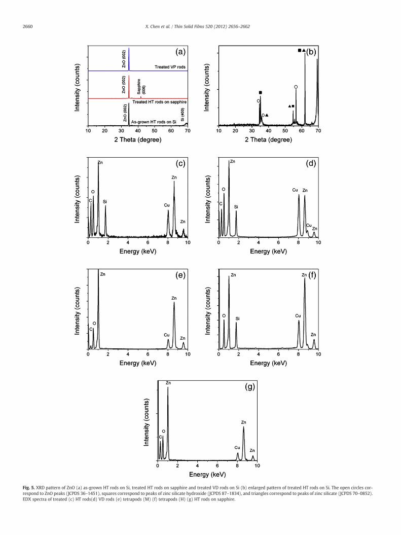
Fig. 5. XRD pattern of ZnO (a) as-grown HT rods on Si, treated HT rods on sapphire and treated VD rods on Si (b) enlarged pattern of treated HT rods on Si. The open circles cor-respond to ZnO peaks (JCPDS 36–1451), squares correspond to peaks of zinc silicate hydroxide (JCPDS 87–1834), and triangles correspond to peaks of zinc silicate (JCPDS 70–0852).EDX spectra of treated (c) HT rods(d) VD rods (e) tetrapods (M) (f) tetrapods (H) (g) HT rods on sapphire.
2660 X. Chen et al. / Thin Solid Films 520 (2012) 2656–2662
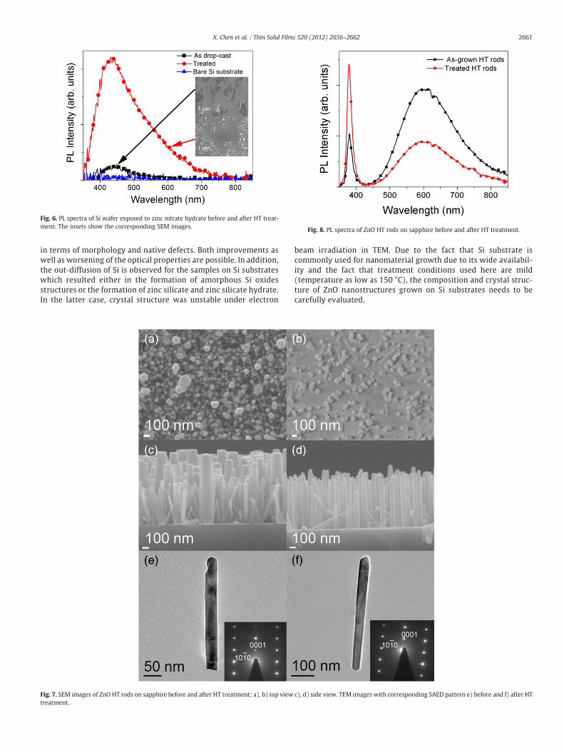
Fig. 6. PL spectra of Si wafer exposed to zinc nitrate hydrate before and after HT treat-ment. The insets show the corresponding SEM images. Fig. 8. PL spectra of ZnO HT rods on sapphire before and after HT treatment.
2661X. Chen et al. / Thin Solid Films 520 (2012) 2656–2662
in terms of morphology and native defects. Both improvements aswell as worsening of the optical properties are possible. In addition,the out-diffusion of Si is observed for the samples on Si substrateswhich resulted either in the formation of amorphous Si oxidesstructures or the formation of zinc silicate and zinc silicate hydrate.In the latter case, crystal structure was unstable under electron
Fig. 7. SEM images of ZnO HT rods on sapphire before and after HT treatment; a), b) top viewtreatment.
beam irradiation in TEM. Due to the fact that Si substrate iscommonly used for nanomaterial growth due to its wide availabil-ity and the fact that treatment conditions used here are mild(temperature as low as 150 °C), the composition and crystal struc-ture of ZnO nanostructures grown on Si substrates needs to becarefully evaluated.
c), d) side view. TEM images with corresponding SAED pattern e) before and f) after HT

2662 X. Chen et al. / Thin Solid Films 520 (2012) 2656–2662
Acknowledgments
Financial support from the project RGC CRF CityU6/CRF/08 and theStrategic Research Theme, University Development Fund, and SmallProject Funding of the University of Hong Kong is acknowledged.
References
[1] A.B. Djurišić, Y.H. Leung, Small 2 (2006) 944.[2] A.B. Djurišić, A.M.C. Ng, X.Y. Chen, Prog. Quantum Electron. 34 (2010) 191.[3] Ü. Özgür, Ya.I. Alivov, C. Liu, A. Teke, M.A. Reshchikov, S. Doğan, V. Avrutin, S.-J.
Cho, H. Morkoç, J. Appl. Phys. 98 (2005) 041301.[4] O. Lupan, T. Pauporté, J. Cryst. Growth 312 (2010) 2454.[5] O. Lupan, V.M. Guérin, I.M. Tiginyanu, V.V. Ursaki, L. Chow,H. Heinrich, T. Pauporté, J.
Photochem. PhotoBiol. A 211 (2010) 65.[6] Z.K. Bai, C.S. Xie, S.P. Zhang, L.X. Zhang, Q.Y. Zhang, W.L. Xu, J. Xu, Sens. Actuators,
B 151 (2010) 107.
[7] M. Ali, M. Winterer, Chem. Mater. 22 (2010) 85.[8] Y.C. Zhong, A.B. Djurišić, Y.F. Hsu, K.S. Wong, G. Brauer, C.C. Ling, W.K. Chan, J.
Phys. Chem. C 112 (2008) 16286.[9] X.Y. Chen, A.M.C. Ng, F. Fang, A.B. Djurišić, W.K. Chan, H.L. Tam, K.W. Cheah,
P.W.K. Fong, H.F. Lui, C. Surya, J. Electrochem. Soc. 157 (2010) H308.[10] A.M.C. Ng, X.Y. Chen, F. Fang, Y.F. Hsu, A.B. Djurišić, C.C. Ling, H.L. Tam, K.W.
Cheah, P.W.K. Fong, H.F. Lui, C. Surya, W.K. Chan, Appl. Phys. B 100 (2010) 851.[11] J.H. Li, D.X. Zhao, X.Q. Meng, Z.Z. Zhang, J.Y. Zhang, D.Z. Shen, Y.M. Lu, X.W. Fan, J.
Phys. Chem. B 110 (2006) 14685.[12] J.P. Richters, T. Voss, D.S. Kim, R. Scholz, M. Zacharias, Nanotechnology 19 (2008)
305202.[13] T.A. Merz, D.R. Doutt, T. Bolton, Y. Dong, L.J. Brillson, Surf. Sci. 605 (2011) L20.[14] Y.X. Du, F.G. Zeng, J. Alloys Compd. 509 (2011) 1275.[15] U. Pal, N. Koshizaki, S.-Y. Terauchi, T. Sasaki, Microsc. Microanal. Microstruct.
8 (1997) 403.[16] L. Storasta, J.P. Bergman, E. Janzen, A. Henry, J. Lu, J. Appl. Phys. 96 (2004) 4909.[17] X.D. Chen, C.L. Yang, M. Gong, W.K. Ge, S. Fung, C.D. Beling, J.N. Wang, M.K. Lui,
C.C. Ling, Phys. Rev. Lett. 92 (2004) 125504.