Embed Size (px)
Citation preview
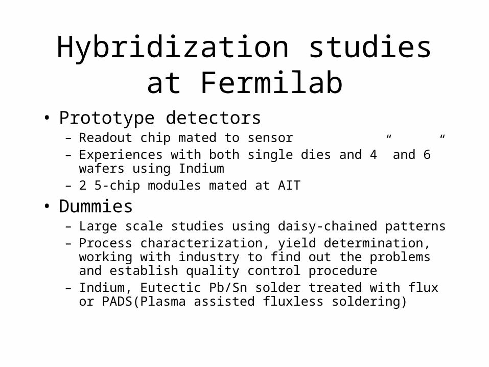
Hybridization studies at Fermilab
• Prototype detectors– Readout chip mated to sensor– Experiences with both single dies and 4” and 6” wafers using
Indium– 2 5-chip modules mated at AIT
• Dummies– Large scale studies using daisy-chained patterns – Process characterization, yield determination, working with
industry to find out the problems and establish quality control procedure
– Indium, Eutectic Pb/Sn solder treated with flux or PADS(Plasma assisted fluxless soldering)

Vendor search
• A lot of enquiries/contacts but most companies are not interested or consider the job too challenging
• Prototyping – BOEING, AIT (both used indium and could do wafer or single dies)
• Dummies – AIT (indium at 30 m pitch)– AIT also tested wafer bumping with 200 m thick
wafers – MCNC/Unitive (solder both flux and fluxless); only 6”
wafers (needs modification for 4”).
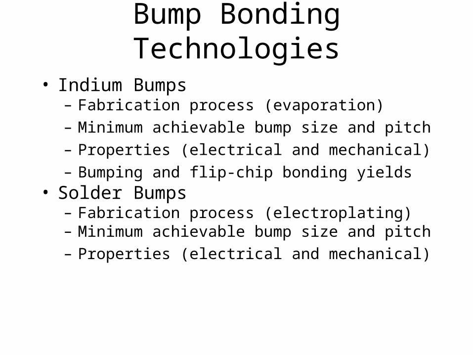
Bump Bonding Technologies
• Indium Bumps– Fabrication process (evaporation)– Minimum achievable bump size and pitch
– Properties (electrical and mechanical)
– Bumping and flip-chip bonding yields• Solder Bumps
– Fabrication process (electroplating)– Minimum achievable bump size and pitch– Properties (electrical and mechanical)

Indium Bumps• Fabricated by thermal evaporation (using a lift-off process) for small bumps, finer
pitch, better uniformity and control, single die bumping possible• Requires sputter deposited 2-metal layer barrier diffusion UBM• Soft compliant bump with a melting point of 156°C• Form a non-conducting oxide layer (which has to be penetrated)• Both sides have to be indium bumped• Minimum bump sizes of 12 µm with a height of 8-10 µm on a 18 µm pitch • Large arrays with 500K+ bumps on a single die possible• Flip-chip bonding using compression only (room temperature process) requiring
~1-2 grams/bump• Bump resistance of ~1-2 Ohms for a 15 µm x 15 µm square bump• Requires a flip-chip bonder with 1-2 micron alignment accuracy and planarization• Expensive to fabricate!

Indium bumps on ROC done at AIT
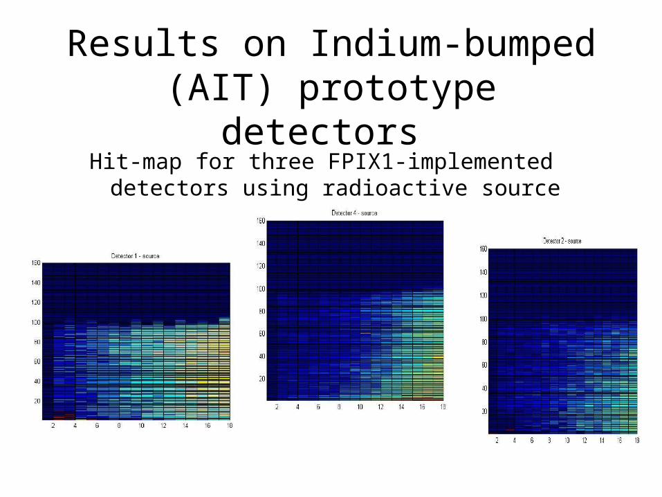
Results on Indium-bumped (AIT) prototype detectors
Hit-map for three FPIX1-implemented detectors using radioactive source

Indium Bumps Summary• Indium bump/bonding is proven, able to fabricate
small bumps on fine pitch (by evaporation) with good mechanical strength and high-yields for both bumping and bonding
• Indium bonding requires bumps on both sides and a highly accurate flip-chip aligner/bonder with planarization capability
• Indium bumps are expensive to fabricate!• Current achievable minimum bump dimensions of 12
µm diameter, height of 8-10 µm, 18 µm pitch

Electroplated Lead-Tin Solder Bumps
• Versatile in selection of solder alloy composition and MP• Self-aligning and self-planarizing bumps (upon reflow)• Requires fabrication of solder bump on one side only with an
opposing "wettable" pad• Excellent electrical and mechanical characteristics:
– low resistance electrical path (2-3 µOhms)– low inductance (~0.1 nH)– shear values in excess of 30 grams for 50 micron bump
• Alpha particle emission from bumps• Potential for low-cost in high volume• Minimum size of 15 µm diameter bumps on a 20 µm pitch!

Eutectic Lead-Tin (37:63) BumpsAfter Reflow @ 215°C
25 micron diameter, 50 micron pitch25 micron diameter, 50 micron pitch

Tests on dummies from MCNC/Unitive
• Structures with 50 m pitch (BTeV) and 150 m pitch(CMS) on same wafer
• 80 PADS single-chip assemblies and 38 fluxed single-chip assemblies (BTeV)
• US-CMS also tested 5 double-chip assemblies and 1 5-chip assembly (using flux-less solder)
• Check connectivity between matched pair of pads using a semi-automatic probe station
• Sometimes, need to apply a low voltage to break through
• Also look for shorts between neighbors

Wafer layout
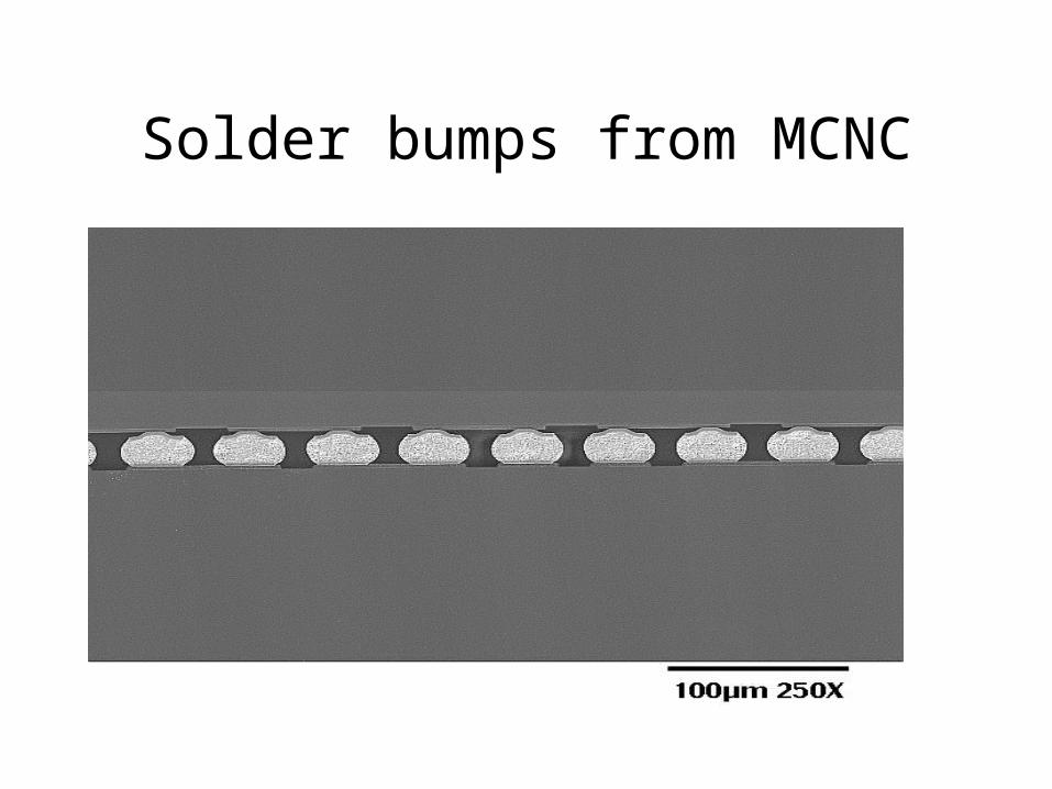
Solder bumps from MCNC
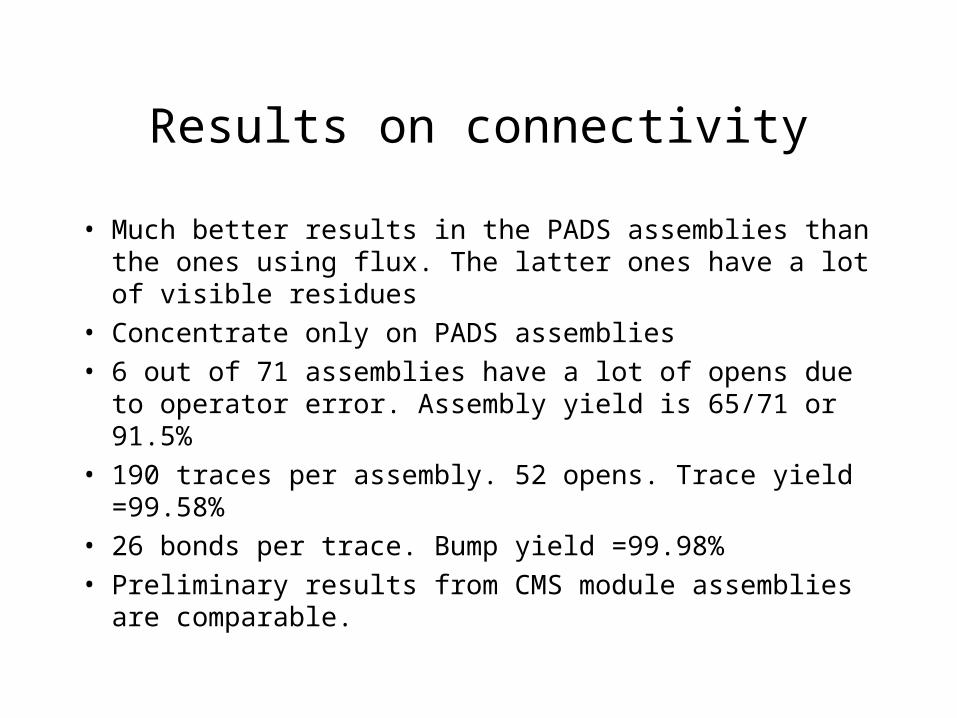
Results on connectivity
• Much better results in the PADS assemblies than the ones using flux. The latter ones have a lot of visible residues
• Concentrate only on PADS assemblies
• 6 out of 71 assemblies have a lot of opens due to operator error. Assembly yield is 65/71 or 91.5%
• 190 traces per assembly. 52 opens. Trace yield =99.58%
• 26 bonds per trace. Bump yield =99.98%
• Preliminary results from CMS module assemblies are comparable.
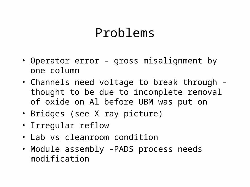
Problems
• Operator error – gross misalignment by one column
• Channels need voltage to break through –thought to be due to incomplete removal of oxide on Al before UBM was put on
• Bridges (see X ray picture)
• Irregular reflow
• Lab vs cleanroom condition
• Module assembly –PADS process needs modification
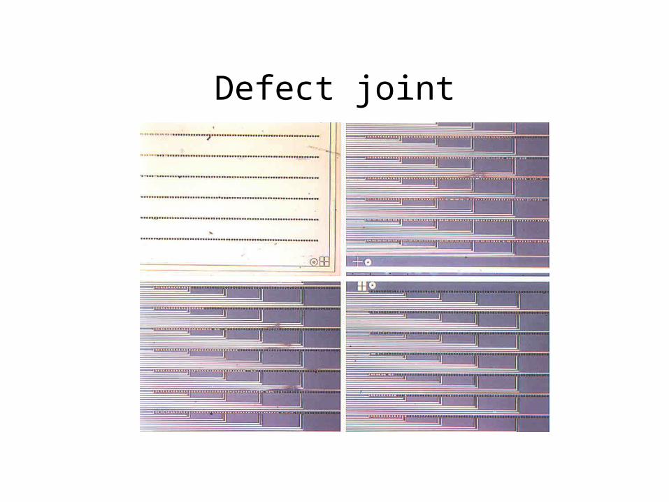
Defect joint

Solder Bumps Summary• Solder bumps may provide an alternative to indium
bump/bonding• Versatile in choice of alloy with MP between 150-
210°C• Current minimum achievable bump sizes of 15 µm
diameter on a 20 µm pitch!• Excellent electrical and mechanical characteristics• Self-aligning and self-planarizing bonding process• Lower fabrication cost than indium requiring bumping
on one side only and a wettable layer on the other
Conclusions
• Satisfactory results on real detectors using Indium
• Dummy tests on 30m ongoing
• Fluxless solder by MCNC has good bond yield
• Whole chip losses need to be better understood and controlled
• Module assembly – non-industrial standard (closely abutted to one another); MCNC needs to learn how to do this
• Next round – real detectors will be bumped and bonded at MCNC