Embed Size (px)
Citation preview

NASA TECHNICALMEMORANDUM
NASA TM X- 68248
(NASA-TH-X-68248) DEVELOPMENT OF AHYBRID MICROELECTRONICS SOLID STATE RELAYFOR 2500 VOLTS ISOLATION AND MINUS 120 CTO 80 C THERMAL CYCLING RANGE (NASA)12 p HC $3.00 CSCL 09A
N73-24235
UnclasG3/09 04692
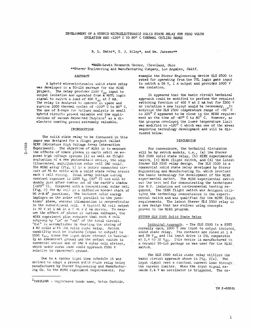
DEVELOPMENT OF A HYBRID MICROELECTRONICS SOLIDSTATE RELAY FOR 2500 VOLTS ISOLATION AND-1200 C TO 800 C THERMAL CYCLING RANGE
by B. L. Sater and T. J. RileyLewis Research CenterCleveland, Ohio 44135
and
Wm. JanssenSterer Engineering and Manufacturing CompanyLos Angeles, California 90038
TECHNICAL PAPER proposed for presentation atPower Electronics Specialists Conference sponsored bythe Institute of Electrical and Electronics EngineersPasadena, California, June 11-13, 1973
00
I-X
(Ai,=
https://ntrs.nasa.gov/search.jsp?R=19730015508 2019-08-16T12:39:07+00:00Z
DEVELOPMENT OF A HYBRID MICROELECTRONICS SOLID STATE RELAY FOR 2500 VOLTSISOLATION AND -1200 C TO 80° C THERMAL CYCLING RANGE
B. L. Sater*, T. J. Riley*, and Wm. Janssen**
*NASA-Lewis Research Center, Cleveland, Ohio**Sterer Engineering and Manufacturing Company, Los Angeles, Calif.
ABSTRACT
A hybrid microelectronics solid state relaywas developed in a TO-116 package for the MINXproject. The relay provides 2500 Vdc input tooutput isolation and operated from a MuilL logicsignal to switch a load of 400 Vdc at 2 mA.The relay is designed to operate in space andsurvive 1000 thermal cycles of -120 ° C to 80° C.The use of X-rays for failure analysis in smallhybrid circuits proved valuable and the appli-cations of vacuum deposited Parylene1 as a di-electric coating proved extremely valuable.
INTRODUCTION
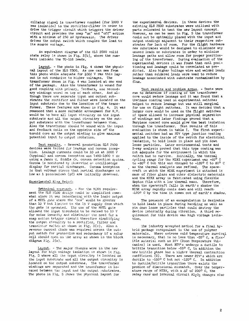
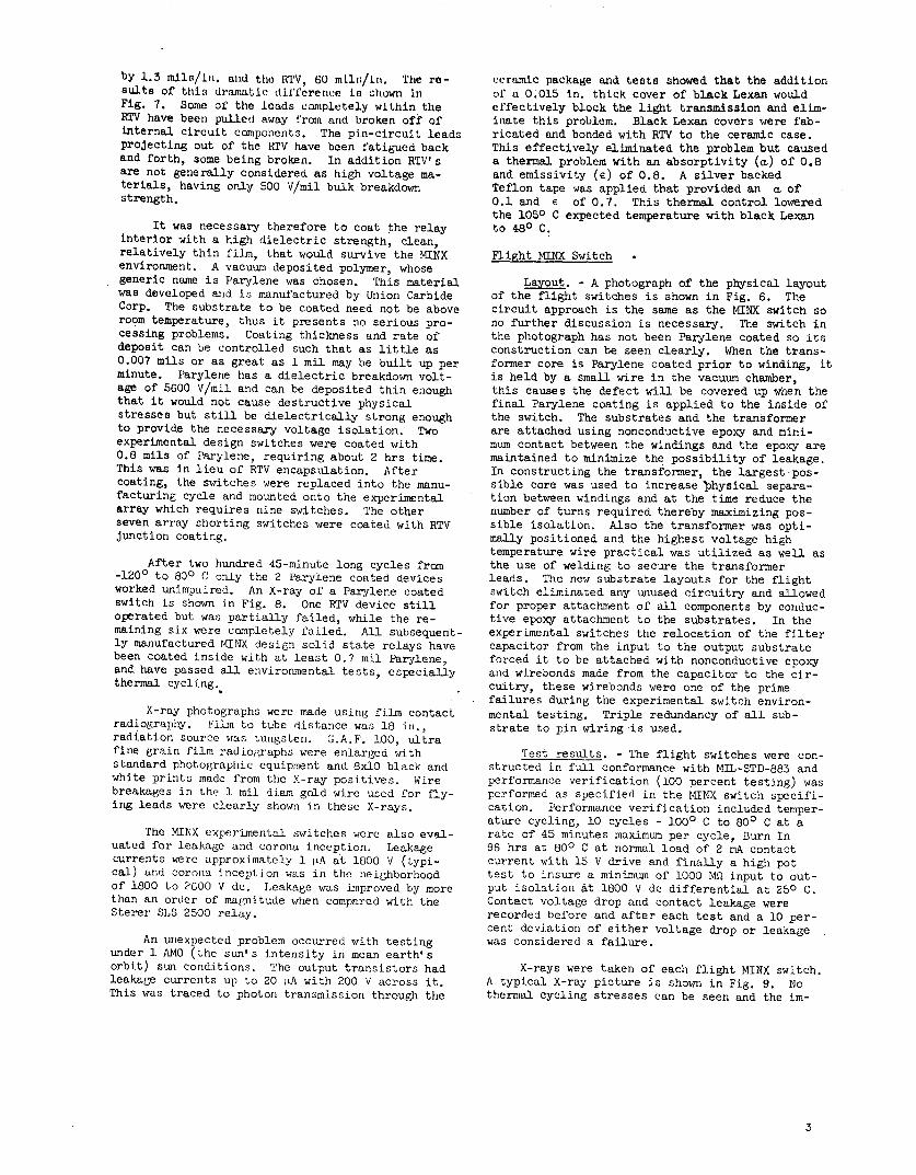
The solid state relay to be discussed in thispaper was designed for a flight project calledMINX (Miniature High Voltage Array InteractionExperiment). The objective of MINX is to measurethe effects of space plasma in earth orbit on ex-posed high voltage systems (1) as well as flightevaluation of a new photovoltaic device, the edgeilluminated, multijunction solar cell (MJ cell).The MINX array (fig. 1) is a series connected cir-cuit-of 36 MJ cells with a solid state relay acrosseach 4 cell string. Total array voltage duringconstant exposure is le00 Vdc (80° C) and will bedouble just after coming out of the earth's shadow(-120 ° C). Compared with a conventional solar cell(fig. 2) the MJ cell is a diffusion bonded stack of96 P-N-N' junctions. The incident solar energyimpinges on the solar cell parallel to the junc-tions' plane, whereas illumination is perpendicularin the conventional cell . A typical MJ cell outputis 40 V at 1 mA in a 2 cm x 2 cm device. To meas-ure the effect of plasma at various voltages, theMINX experiment plan requires that each 4 cellsubgroup by "in" or "out" of the total circuit."Out" is accomplished by shorting the string of4 MJ cells with the solid state relay. Switchcapability must be isolated (input to output) to2500 V,*<, since the input drive circuit is basical-ly at spacecraft ground and the output switch isconnected across one of the 4 solar cell strings,which under worse case could approach 2500 Vrelative to spacecraft ground.
Due to a rather tight time schedule it wasdecided to adapt a proven solid state relay beingmanufactured by Storer Engineering and Manufactur-ing Co. to the MINX experiment requirements. For
example the Sterer Engineering device SLS 2500 israted for operating from the TTL logic gate inputto switch a 28 V, 1 A output and provides 1000 Vrms isolation.
It appeared that the basic circuit technicalapproach could be modified to perform the requiredswitching function of 400 V at 2 mA but for 2500 Vdc isolation a new layout would be necessary. 0 Inaddition the SLS 2500 temperature range of -55 Cto 125° C appeared to be close to the MINX require-ment at the time of -60° C to 800 C. However, asthe program developed the lower temperature limitwas modified to -120 ° C which was one of the areasrequiring technology development and will be dis-cussed below.
DISCUSSION
For convenience, the technical discussionwill be by switch models, i.e., (a) the StererSLS 2500 solid state relay, (b) MINX experimentalswitch, (c) MINX flight switch, and (d) the latestSterer SLS 2500 relay design. The SLS 2500 is acommercial solid state relay developed by StererEngineering and Manufacturing Co. which providedthe basic technology for development of the MINXexperimental switch. The MINX experimental switchwas the test bed for demonstrating the techniquesfor H.V. isolation and environmental testing re-quired. The MINX flight switch was designed util-izing the technology demonstrated in the experi-mental switch and was qualified for the MINX flightrequirements. The latest Sterer SLS 2500 relay isa new design that has evolved using conceptsproven in the MINX program.
STERER SLS 2500 Solid State Relay
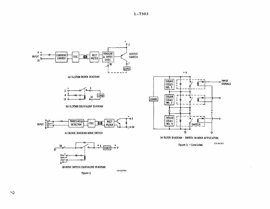
Technical approach. - The SLS 2500 is a SPSTnormally open, 1000 V rms input to output isolated,solid state relay. Its contacts are rated at 1 Aand 28 Vdc and its input drive is TTL compatibleat 2.4 to 32 Vdc. This device is manufactured ina ceramic TO-116 package as was used for the MINXswitch.
The SLS 2500 solid state relay utilizes thebasic circuit approach shown in Fig. 3(a). Theinput signal sees a constant current load throughthe current limiter. When the input signal ex-ceeds 2.4 V an oscillator is triggered. The os-
1PARYLENE - registered trade nmne, Union Carbide.
TM X-68248
1
0r0
cillator signal is transformer coupled (for 1000 Vrms isolation) to the rectifier-filter in order todrive the trigger circuit which triggers the (trivercircuit and provides the snap "on" and "off" actionwith a minimum of 250 mV hysteresis. lThe driverdrives the output switch which couples the load toits source voltage.
An equivalent diagram of the SLS 2500 solidstate relay is shown in Fig. 3(b), where the num-bers indicate the TO-116 leads.
Layout. - The photo in Fig. 4 shows the physi-cal layout of the SLS 2500. As one can see fromthis photo while adequate for 1000 V rms this lay-out is not conducive to higher voltages. Thetransformer shown in Fig. 4 was located at one endof the package. Also the transformer is wound forgood coupling with primary, feedback, and second-ary windings wound on top of each other. And al-though there are separate input and output sub-strates the rectifier and filter were located on theinput substrate due to the location of the trans-former. These features are shown in Fig. 4. It wasreasoned that a more suitable arrangment for H.V.would be to have all input circuitry on the inputsubstrate and all the output circuitry on the out-put substrate with the transformer between them.Also the transformer should be wound with the inputand feedback coils on the opposite side of' thetoroid core as the output winding to give maximumpotential input to output isolation.
Test results. - Several production SLS 2500devices were tested for leakage and corona incep-tion. Leakage currents could be 10 pA at 1000 V(typical) and corona inception was 1400-1800 V dcusing a James G. Biddle Co. corona detection system.Corona is monitored by observing an oscilloscopedisplay for partial discharges. Corona inceptionis that voltage stress that partial discharges aslow as 1 picocoulomb (pC) are initially observed.
Experimental Minx Switch
Technical altproach. - For the MINX require-ment the SLS ?500 design could be simplified some-what since it was interfacing with the logic outputof a MIriTL gate where the "one" would be greaterthan 10 V but limited to the 15 V supply from whichthe gate is operated. The use of the MJFL gateallowed the input threshold to be raised to 10 Vfor noise immunity and eliminated the need for asnap action trigger circuit therefore simplifyingthe output. circuitry to a rectifier, filter andtransistor switch as shown in Fig. 3(c). Also areverse current diode was required across the out-put switch for protection and redundancy if a solarcell should open on the array as shown in the blockdiagram Fig. 5(e).
Layout. - The major changes were in the newlayout for high voltage isolation as shown in Fig.Fig. 5 where all the input circuitry is located onthe input substrate and all the output circuitry islocated on the output substrate. The transformerwindings are separated and the transformer is lo-cated between the input and the output substrates.The photo in Fig. 5 shows the physical layout for
the experimental devices. In these devices theexisting SLS 2500 substrates were utilized withparts relocated to test the new layout concept.However, as can be seen in Fig. 5 the transformercould not be optimally placed with the input andoutput windings adjacent to their respective sub-strates for lack of room. For the flight hardwarenew substrates would be designed to eliminate anyunused leads on substrates in order to minimizeleakage paths and allow room for proper position-ing of the transformer. During evaluation of theexperimental devices it was found that coil posi-tioning and leakage could be correlated as pre-dicted. Also higher voltage wire and welded leadsrather than soldered leads were used to reduceleakage associated with substrate contamination byflux.
Test results and problem areas. - Tests wererun to determine if coating of the transformercore would reduce leakage and it was found that aUrethane coating used on experimental switcheshelped to reduce leakage but was still marginalfor use on flight switches. It was decided that alarger core would be used on the flight switchesif space allowed to increase physical separationof windings and later findings proved that aParylene coated core would give the best isolationthrough the transformer, Test results of thisevaluation is shown in table I. The first experi-mental switches had an RTV type junction coatingapplied to the inside of the switch for electricalisolation, to hold leads in place and pin downloose particles. Later environmental tests andX-ray analysis proved that this type coating wasnot adequate for the environment in which theswitch had to survive. Initially, the thermalcycling range for the MINX experiment was -60° Cto +80° C but this was changed to -120o C to 80° Cas the thermal analysis was refined. The space-craft on which the MINX experiment is attached ismade of fiber glass and other dielectric materialsand the MINX array is fabricated using flexibleKapton film with a low thermal mass. Therefore,when the spacecraft falls in earth's shadow theMINX array rapidly. cools down and will reach.-1200 C by the time it comes out of earth's shadow.
The presence of an encapsulation is desirableto hold leads in place during handling as well aspin down loose particles that could destroy thedevice internally during vibration. A third re-quirement for this device was high voltage isola-tion.
The industry accepted method for a final hy-brid package encapsulant is the use of polymermaterials. Where extreme cold temperature survivalis necessary, that is no less than -55° C, a flex-'ible material such as RTV (Room Temperature Vul-canize) is used. Most RTV's undergo a ductile tobrittle transition below -55° C, in addition thenew brittle phase has a higher thermal contractioncoefficient (2). There are newer RTV's which areductile to -110° C but not -120° C. In additionto ductile/brittle transition there exists theproblem of dimensional mismatch. Over the temper-ature range of MINX, with a AT of 200° C, therelay case' and internal circuit A1203 changes size
2
by 1.3 mils/in. and the RTV, 60 mlls;/Ln. The re-sults of this dramatic difference is Khown inFig. 7. Some of the leads completely within theRTV have been pulled away from and broken off ofinternal circuit components. The pin-circuit leadsprojecting out of the RTV have been fatigued backand forth, some being broken. In addition RTV'sare not generally Considered as high voltage ma-terials, having only 500 V/mil bulk breakdownstrength.
It was necessary therefore to coat the relayinterior with a high dielectric strength, clean,relatively thin film, that would survive the MINXenvironment. A vacuum deposited polymer, whosegeneric name is Parylene was chosen. This materialwas developed and is manufactured by Union CarbideCorp. The substrate to be coated need not be aboveroom temperature, thus it presents no serious pro-cessing problems. Coating thickness and rate ofdeposit can be controlled such that as little as0.007 mils or as great as 1 mil may be built up perminute. Parylene has a dielectric breakdown volt-age of 5600 V/mil and can be deposited thin enoughthat it would not cause destructive physicalstresses but still be dielectrically strong enoughto provide the necessary voltage isolation. Twoexperimental design switches were coated with0.8 mils of Parylene, requiring about 2 hrs time.This was in lieu of RTV encapsulation. Aftercoating, the switches were replaced into the manu-facturing cycle and mounted onto the experimentalarray which requires nine switches. The otherseven array shorting switches were coated with RTVJunction coating.
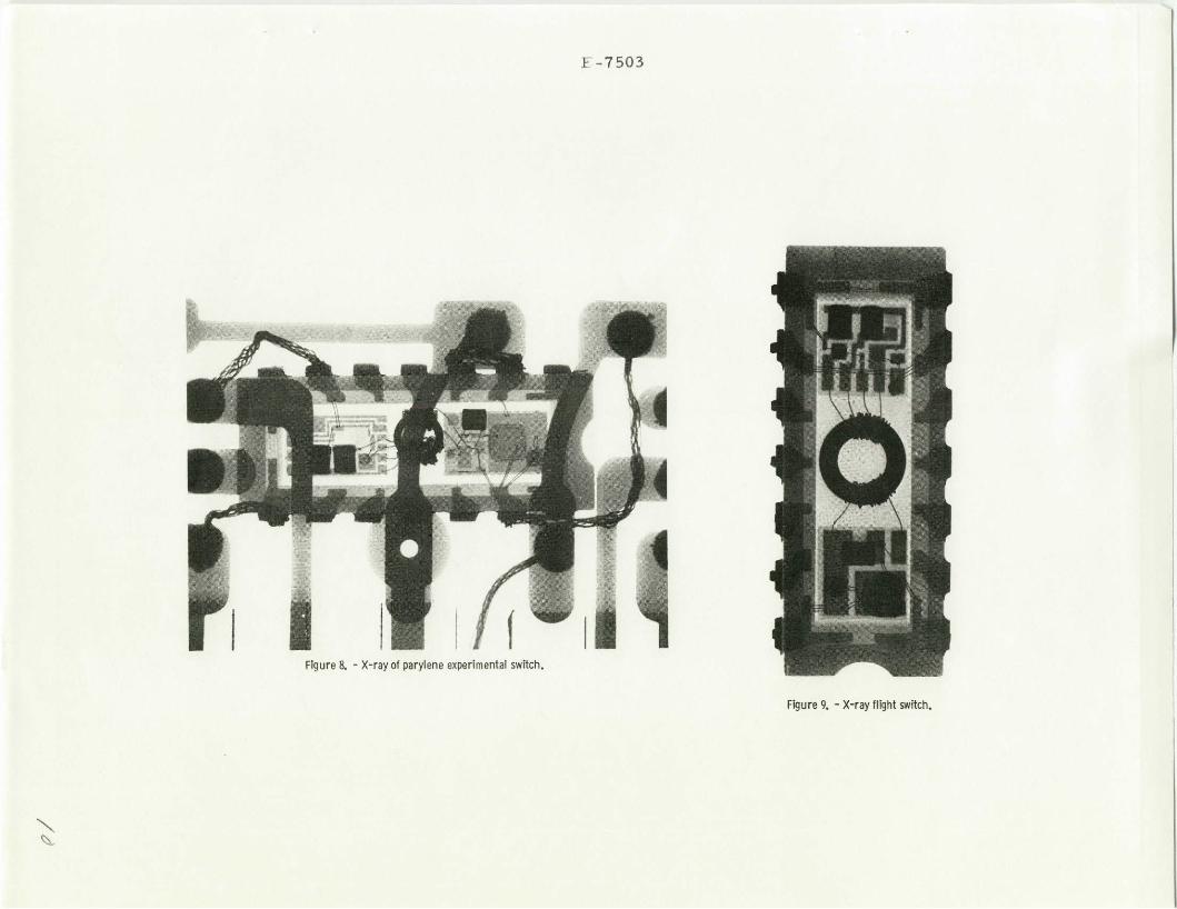
After two hundred 45-minute long cycles from-120 ° to 80° C only the 2 Parylene coated devicesworked unimpaired. An X-ray of a Parylene coatedswitch is shown in Fig. 8. One RTV device stilloperated but was partially failed, while the re-maining six were completely failed. All subsequent-ly manufactured MINX design solid state relays havebeen coated inside with at least 0.7 mil Parylene,and have passed all environmental tests, especiallythermal cycling.
X-ray photographs were made using film contactradiography. Film to tube distance was 18 in.,radiation source was tungsten. G.A.F. 100, ultrafine grain film radiographs were enlarged withstandard photographic equipment and 8xl0 black andwhite prints made from the X-ray positives. Wirebreakages in the 1 mil diem gold wire used for fly-ing leads were clearly shown in these X-rays.
The MINX experimental switches were also eval-uated for leakage and corona inception. Leakagecurrents were approximately 1 I-A at 1800 V (typi-cal) and corona inception was in the neighborhoodof 1800 to 2GOO V dc. Leakage was improved by morethan an order of magnitude when compared with theSterer SLS 2500 relay.
An unexpected problem occurred with testingunder 1 AMO (the sun's intensity in mean earth'sorbit) sun conditions. The output transistors hadleakage currents up to 20 pA with 200 V across it.This was traced to photon transmission through the
cratnLc package and tests showed that the additionof a 0.015 in. thick cover of black Lexan wouldeffectively block the light transmission and elim-inate this problem. Black Lexan covers were fab-ricated and bonded with RTV to the ceramic case.This effectively eliminated the problem but causeda thermal problem with an absorptivity (a) of 0.8and emissivity (e) of 0.8. A silver backedTeflon tape was applied that provided an m of0.1 and E of 0.7. This thermal control loweredthe 1050 C expected temperature with black Lexanto 48° C.
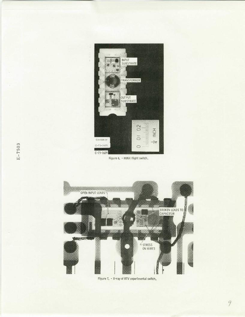
Flight MINX Switch -
Layout. - A photograph of the physical layoutof the flight switches is shown in Fig. 6. Thecircuit approach is the same as the MINX switch sono further discussion is necessary. The switch inthe photograph has not been Parylene coated so itsconstruction can be seen clearly. When the trans-former core is Parylene coated prior to winding, itis held by a small wire in the vacuum chamber,this causes the defect will be covered up when thefinal Parylene coating is applied to the inside ofthe switch. The substrates and the transformerare attached using nonconductive epoxy and mini-mum contact between the windings and the epoxy aremaintained to minimize the possibility of leakage.In constructing the transformer, the largest pos-sible core was used to increase physical separa-tion between windings and at the time reduce thenumber of turns required thereby maximizing pos-sible isolation. Also the transformer was opti-mally positioned and the highest voltage hightemperature wire practical was utilized as well asthe use of welding to secure the transformerleads. The new substrate layouts for the flightswitch eliminated any unused circuitry and allowedfor proper attachment of all components by conduc-tive epoxy attachment to the substrates. In theexperimental switches the relocation of the filtercapacitor from the input to the output substrateforced it to be attached with nonconductive epoxyand wirebonds made from the capacitor to the cir-cuitry, these wirebonds were one of the primefailures during the experimental switch environ-mental testing. Triple redundancy of all sub-strate to pin wiring is used.
Test results. - The flight switches were con-structed in full conformance with MIL-STD-883 andperformance verification (100 percent testing) wasperformed as specified in the MINX switch specifi-cation. Performance verification included temper-ature cycling, 10 cycles - 100° C to 80° C at arate of 45 minutes maximum per cycle, Burn In96 hrs at 80° C at normal load of 2 mA contactcurrent with 15 V drive and finally a high pottest to insure a minimum of 1000 MS input to out-put isolation at 1800 V dc differential at 25° C.Contact voltage drop and contact leakage wererecorded before and after each test and a 10 per-cent deviation of either voltage drop or leakagewas considered a failure.
X-rays were taken of each flight MINX switch.A typical X-ray picture is shown in Fig. 9. Nothermal cycling stresses can be seen and the im-
3
proved layout and transformer winding is apparent.
In the flight units the Parylene coated coresand new layout demonstrated dramatic improvementsin leakage and corona inception. Leakage currentsmeasured with Hewlitt Packard high resistancemeter (Model HP4329A) were less than 0.001 PA at1000 V dc. This represents an isolation resistanceof greater than 101 2 S at 1000 V. No corona wasdetected in any flight units tested to 3000 V dcminimum. Two units were tested to breakdown andcorona inception was observed in the 5.5 to 6.0 kVrange. Breakdown occurred in the 7 to 8 kV region.
Two flight MINX switches were exposed to 1 MeVelectron radiation to 1015 electrons/cm2 dose. Theinput trigger level increased slightly and the out-put saturated voltage drop decreased slightly.Both of these trends are to be expected with re-duced gain of the transistors. However, leakageremained less than 0.001 PA at 1000 V and no coronawas detected to 3000 V dc as typically observed inall flight units.
At the time of this writing, no problems havebeen experienced with the flight MINX switches.
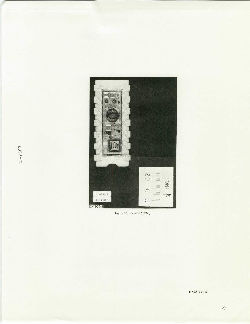
SLS 2500 Redesign
The production SLS 2500 was redesigned andphysically relayed out as best possible maintainingthe same pin configuration and electrical specifi-cations to incorporate the desirable featuresproven through extensive testing of the MINXswitch.
The new SLS 2500 layout is shown in photo-graph in Fig. 10. The windings were separated inthe transformer, high voltage high temperaturewire is used to wind it, the core is epoxy coated,the coil wires are attached by welding, and thecoil is properly positioned between the input andoutput circuitry on the substrate. The utilizationof these techniques increased the yield of SLS2500's in production by lowering the number ofunits failed foi lack of required isolation.
CONCLUSION
A hybrid microelectronics solid state relaywas successfully developed in a TO-116 ceramic case
for the MINX project that provides 2500 V de inputto output isolation. The relay was designed tooperate in space and survive 1000 thermal cycles of-1200 C to 80o C.
The use of enlarged pictures from X-rays foranalysis of failed hybrid experimental units provedextremely valuable in evaluating RTV and Parylenecoatings' stress due to thermal cycling. Thesepictures clearly showed cyclic stress on flyingleads where differences between thermal expansionof materials was a problem. In addition shearedleads in failed units can be clearly observed.Vacuum deposited Parylene with its 5600 V/mil di-electric strength and ability to be applied in thinapplications proved indispensable. Parylene wasused to insulate the transformer core prior towinding and to coat the internal assembly prior toenclosing. With Parylene, thermal cycling from-120o C to 80° C appeared to be stress free pri-marily because the Parylene can be applied in uni-form thin applications.
In this small package (TO-116 size) devicesappear to be clean in corona up to 5000 V dc andthe isolation built into the transformer appearsto be as good as that inherent in the package it-self.
Radiation degradation was riot apparent in thisdesign and the microelectronics solid state relaydeveloped appears fully space qualified for theMINX experiment.
REFERENCES
(1) Plasma Reports:(a) W. Knauer, et al., "High Voltage Solar
Array Study," Hughes Research Labs.,NASA CR-72675, 1970.
(b) W. F. Springgate, and H. Oman, "HighVoltage Solar Array Study," The BoeingCo., D2-121734-1, NASA CR-72674, 1969.
(2) A. M. Solama, et al., "Stress Analysis andDesign of Silicon Cell Arrays and RelatedMaterial Problems," Jet Propulsion Lab.,Tech. Rep. 32-1557, Mar. 1, 1972.

TABLE I. - TRANSFORMER ISOLATION TESTS
[Leakage current in 4A vs voltage stress]
Voltage stress, V dc
500 1000 1500 2000 2500 3000
Leakage currents for:
Old XFM'R - Uncoated 0.2 tA 0.6 [A 1.2 [A 1.9 MA 3.0 MA 5.0 4A
Old XFM'R - Urethane <0.001 <0.001 <0.001 1.4 2.3 5.6
New XFM'R - Uncoated 0.1 0.38 0.9 2.0 3.5 6.0
New XFM'R - Urethane <0.001 <0.001 <0.001 2.2 4.5 6.0
New XFM'R - Parylene <0.001 <0.001 <0.001 <0.001 <0.001 <0.001
Old XFM'R - small core,New XFM'R - large core,
25:25:50 windings9:9:18 windings
C.-
MINX FLIGHT ARRAY
KAPTON SUBSTRATE WITH FLEXIBLE PRINTED /CIRCUITRY MOUNTED ON LEXAN FRAME
Figure L - MINX flight array. CS-66786
Cn
LnOt
[,,.
CONVENTIONAL CELL 2 x 2 CM MULTIJUNCTION (96),EDGE ILLUMINATED CELL 2 x 2 CM
MAX = 125 mA IM x = 1. 12 mAVMAX =0.47 V VMAX = 40 V
VWITH ANTI REFLECTION COATINGS 1280 C TYPICAL)CS-66788
Figure 2. - Multiple junction edge illuminated solar cell.
E-7503
+
2
4 + TR OUTPUTINPUT CURRENT Osc SWITCH0LIMITER I ITR &DIESIC
L ------ + V
(a) SLS2500 BLOCK DIAGRAM
SOLAR F ..CELLS
4+2 o4 S 3 LOAD SOA--i- - - -----4010 -11 LAS A'LJC NO. L o- -_ _,
(b) SLS2500 EQUIVALENT DIAGRAM
6+ THIRESHOLD CLLINPUT 7 o -DETECTORTOR C NO _/- SWITCH
- 14-
(c) BLOCK DIAGRAM MINX SWITCH'e) BLOCK DIAGRAM - SWITCH IN MINX
14 +1 + Figure 3. -Concluded.I T
6+.6i93,78(d) MINX SWITCH EQUIVALENT DIAGRAM
CS-66789Figure 3.
APPLICATION
CS-66787

E-7503
RECTIFIERFILTERCIRCUITRY INPUT CIR-INPUT
SUBSTRATE
OUTPUTCIRCUITRY OUTPUTSUBSTRATE SUBSTRATE
cs-66840
736 27 -73-168
I--73-1621
C-73-1627 Figure 5. - MINX experimental switch.
Fiqure 4. - SLS 2500 solid state relay.
INPUT" SUBSTRATE
O-
- TRANSFORMER
OUTPUT6UBSTRATE
i -(D
0Ln-
SC-73-1629I
Figure 6. -MINX flight switch.
OPEN INPUT LEADS
BROKEN LEADS TOCAPACITOR
ZSTRESS
ON WIRES
Figure 7. -X-ray of RTV experimental switch.
E-7503
Figure 8. - X-ray of parylene experimental switch.
Figure 9. - X-ray flight switch.
Nl
o
l -
C-73-2046 .
C-73-2046
Figure 10. - New SLS 2500.
NASA-Lewis
7/