Embed Size (px)
Citation preview

TABLE I. SUMMARY OF STRENGTHS AND WEAKNESSES OF LARGE-AREA ELECTRONICS AND CMOS ICS
CMOS ICS LARGE-AREA
ELECTRONICS
Sensing Size-limited, sparse arrays
Highly-dense, macroscopic arrays; flexible substrates
Energy Harvesting
Efficient power management circuits
Expansive energy harvesters for substantial power
Computation & Instrumentation
CMOS transistors provide high efficiency and rich functionality
Low-performance thin-film transistors and thin-film diodes
Hybrid Large-Area Systems: Challenges in Interfacing
Tiffany Moy, Sigurd Wagner, Warren Rieutort-Louis, Yingzhe Hu, Liechao Huang, Josue Sanz-Robinson, James C. Sturm, Naveen Verma
Department of Electrical Engineering Princeton University Princeton, NJ, USA
Abstract—Hybrid large-area systems aim to leverage the strengths of two complementary technologies: (1) large-area electronics (LAE), which enables dense arrays of diverse transducers on substrates that can be large and flexible; and (2) silicon CMOS ICs, which enable efficient and high-performance instrumentation, computation, and power management. A key challenge in realizing these hybrid systems on a large-scale lies in the interfacing required between the two technologies. We describe methods to ease the interfacing, enabled by device, circuit, and algorithmic advances, thereby suggesting a range of challenges and opportunities that are exposed when thinking about systems.
Keywords—large-area electronics (LAE), hybrid systems, thin-film sensors, thin-film transistors (TFTs).
I. INTRODUCTION Large-area electronics (LAE) is based on low-temperature
processing of semiconducting and insulating thin-films. As such, this technology allows the use of a wide range of materials to create a diverse catalog of transducers for sensing [1]-[4]. Another key benefit of the low temperature used in LAE is that it enables processing over large, expansive areas (on the order of m2), and is compatible with a variety of substrates with various form factors, such as plastic or glass. Thus, by using LAE to create vast, yet dense, arrays of sensors on conformal substrates, we are able to obtain a wealth of information from the surrounding macroscopic, physical world.
However, processing the resulting large amounts of sensor data to obtain such information is a task unsuited for LAE. The same low-temperature processing that enables the aforementioned sensing capabilities of LAE, causes low performance in the thin-film devices employed, primarily thin-film transistors (TFTs) and thin-film diodes (TFDs). For example, amorphous silicon (a-Si) TFTs, prominent devices in the flat-panel display industry today, have low mobilities (~1cm2/Vs) and high threshold voltages (>1V). On the other hand, CMOS ICs, with transistors having orders-of-magnitude better performance than TFTs, are more appropriate for performing computational functions, particularly on the large scales envisioned. Table I summarizes the strengths and weaknesses of these two technologies with respect to the key function in hybrid sensing systems; in addition to sensing and computation abilities, energy harvesting is important for self-powering considerations. Indeed, it is clear that hybrid LAE-CMOS systems, which marry the complementary strengths of
the two technologies, are appealing for large-scale sensing applications.
However, as we scale the level of sensing for future applications, a high number of interfaces between the LAE sensors and the corresponding CMOS ICs become necessary. These interfaces pose a crucial limitation on the viability of large-scale hybrid systems. To realize such systems we require interfacing solutions that maximize robustness, minimize cost and enable scalability. Specifically, we need to: (1) minimize the assembly complexity and reliability risks of each physical interface, and (2) minimize the total number of interfaces.
The methods used to address the interfacing challenges today are exemplified in commercial flat-panel displays. In these displays, an active matrix is used to access the sensors. By selectively enabling a particular row and column, a corresponding sensor can be accessed. Using this design, the number of required interfaces is reduced by approximately a square-root factor. These interfaces are then coupled to CMOS driver and readout ICs via metallurgical bonding.
However, while flat-panel displays certainly raise and address the aforementioned interfacing issues in part, the solutions employed are not applicable to all hybrid systems. First, metallurgical bonding is not adequate for many of the envisioned applications because of its cost and sensitivity to bending when applied to flexible substrates. As well, while an active matrix reduces the number of interfaces, it still scales rather strongly with the number of sensors, which can be very large, covering many square meters of surface. Furthermore, active matrices are most advantageous when accessing regularly-spaced sensor arrays. Irregular sensor arrangements call for more flexible approaches to LAE-CMOS interfacing.
Funding provided by NSF (grants ECCS-1202168 and CCF-1218206) and Systems on Nanoscale Information fabriCs (SONIC), one of six SRC STARnet Centers, sponsored by MARCO and DARPA.
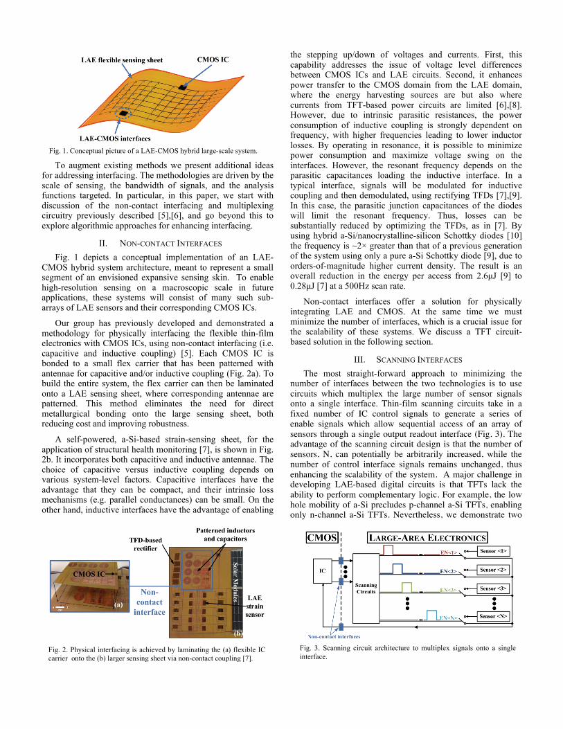
Fig. 2. Physical interfacing is achieved by laminating the (a) flexible IC carrier onto the (b) larger sensing sheet via non-contact coupling [7].
Fig. 3. Scanning circuit architecture to multiplex signals onto a single interface.
Fig. 1. Conceptual picture of a LAE-CMOS hybrid large-scale system.
To augment existing methods we present additional ideas for addressing interfacing. The methodologies are driven by the scale of sensing, the bandwidth of signals, and the analysis functions targeted. In particular, in this paper, we start with discussion of the non-contact interfacing and multiplexing circuitry previously described [5],[6], and go beyond this to explore algorithmic approaches for enhancing interfacing.
II. NON-CONTACT INTERFACES Fig. 1 depicts a conceptual implementation of an LAE-
CMOS hybrid system architecture, meant to represent a small segment of an envisioned expansive sensing skin. To enable high-resolution sensing on a macroscopic scale in future applications, these systems will consist of many such sub-arrays of LAE sensors and their corresponding CMOS ICs.
Our group has previously developed and demonstrated a methodology for physically interfacing the flexible thin-film electronics with CMOS ICs, using non-contact interfacing (i.e. capacitive and inductive coupling) [5]. Each CMOS IC is bonded to a small flex carrier that has been patterned with antennae for capacitive and/or inductive coupling (Fig. 2a). To build the entire system, the flex carrier can then be laminated onto a LAE sensing sheet, where corresponding antennae are patterned. This method eliminates the need for direct metallurgical bonding onto the large sensing sheet, both reducing cost and improving robustness.
A self-powered, a-Si-based strain-sensing sheet, for the application of structural health monitoring [7], is shown in Fig. 2b. It incorporates both capacitive and inductive antennae. The choice of capacitive versus inductive coupling depends on various system-level factors. Capacitive interfaces have the advantage that they can be compact, and their intrinsic loss mechanisms (e.g. parallel conductances) can be small. On the other hand, inductive interfaces have the advantage of enabling
the stepping up/down of voltages and currents. First, this capability addresses the issue of voltage level differences between CMOS ICs and LAE circuits. Second, it enhances power transfer to the CMOS domain from the LAE domain, where the energy harvesting sources are but also where currents from TFT-based power circuits are limited [6],[8]. However, due to intrinsic parasitic resistances, the power consumption of inductive coupling is strongly dependent on frequency, with higher frequencies leading to lower inductor losses. By operating in resonance, it is possible to minimize power consumption and maximize voltage swing on the interfaces. However, the resonant frequency depends on the parasitic capacitances loading the inductive interface. In a typical interface, signals will be modulated for inductive coupling and then demodulated, using rectifying TFDs [7],[9]. In this case, the parasitic junction capacitances of the diodes will limit the resonant frequency. Thus, losses can be substantially reduced by optimizing the TFDs, as in [7]. By using hybrid a-Si/nanocrystalline-silicon Schottky diodes [10] the frequency is ~2× greater than that of a previous generation of the system using only a pure a-Si Schottky diode [9], due to orders-of-magnitude higher current density. The result is an overall reduction in the energy per access from 2.6µJ [9] to 0.28µJ [7] at a 500Hz scan rate.
Non-contact interfaces offer a solution for physically integrating LAE and CMOS. At the same time we must minimize the number of interfaces, which is a crucial issue for the scalability of these systems. We discuss a TFT circuit-based solution in the following section.
III. SCANNING INTERFACES The most straight-forward approach to minimizing the
number of interfaces between the two technologies is to use circuits which multiplex the large number of sensor signals onto a single interface. Thin-film scanning circuits take in a fixed number of IC control signals to generate a series of enable signals which allow sequential access of an array of sensors through a single output readout interface (Fig. 3). The advantage of the scanning circuit design is that the number of sensors, N, can potentially be arbitrarily increased, while the number of control interface signals remains unchanged, thus enhancing the scalability of the system. A major challenge in developing LAE-based digital circuits is that TFTs lack the ability to perform complementary logic. For example, the low hole mobility of a-Si precludes p-channel a-Si TFTs, enabling only n-channel a-Si TFTs. Nevertheless, we demonstrate two

Fig. 4. Fully-passive TFT scanning circuit for sequential accessing of sensors [7], [9].
Fig. 5. Active TFT scanning circuit for sequential accessing of sensors [12].
scanning circuit topologies, which use only n-channel TFTs: a fully-passive circuit design and an active circuit design.
A. Fully-Passive TFT Scanning Circuit In [7],[9] a fully-passive a-Si TFT-based scanning circuit,
requiring only 4 control signals from the CMOS IC, is used to multiplex sensor outputs onto a single channel (Fig. 4). The circuit essentially operates by passing a token, the enable signal, down the elements of the chain. With only n-channel TFTs, to preserve the voltage level of the enable signal as it cascades down the chain of sensors, capacitive bootstrapping is used. This necessitates three-phase control: (1) precharging, (2) driving, and (3) resetting the bootstrap capacitor.
When no LAE power supply drives this circuit, inductive coupling is required to step-up the voltage of the control signals from CMOS to LAE, in order to meet the operational voltage requirements of the TFTs. As mentioned, the drawback of using inductive interfaces is larger power consumption due to parasitic losses in the inductors. However, the development of an on-sheet LAE power supply based on solar cells, thin form factor batteries, and battery management circuits [11] enables the use of active circuit topologies. Such circuits are no longer dependent on inductor step-up to generate the appropriate control signal voltages required for TFT operation.
B. Active TFT Scanning Circuit An alternate active scanning circuit was demonstrated [12]
that requires only 3 control signals from the CMOS IC, transmitted to LAE via capacitive interfaces (Fig. 5). The signals are fed into level-converter stages, to generate the large voltage swings needed to drive the scanning elements. Each scanning element operates by explicitly discharging and charging the nodes of an output capacitor, Cint, to generate the logic-high and logic-low voltages of the enable signal. With this design, the logic-high achieves voltages close to the supply rail. As well, the static power consumption of low-logic scanning blocks is negligible, implying that scaling the number of sensors, and thus number of scanning elements, does not increase the overall power consumption.
While the scanning circuits can significantly address interfacing limitations in certain applications a solution using only scanning circuits is not always sufficient. For instance, the scanning speed of the active circuit is determined by a time constant that depends on RL and Cint, which are set by properties of the TFTs. That is, RL and Cint must be appropriately sized to be able to pull down the XSCAN node and to drive the capacitance of the following stage, respectively. For applications that demand signals of greater bandwidth, the limited speed of the scanning circuit caps the allowable number of elements within a sensing array, due to Nyquist sampling considerations. For example, in a human-voice acquisition system based on an array of thin-film microphones [13], the speed of a-Si TFT scanning circuits is limited to ~20kHz while the bandwidth of the input speech signals is ~10kHz. Under Nyquist-sampling constraints, this limits the maximum number of signal channels to less than 2. However, by incorporating a sub-Nyquist reconstruction algorithm in conjunction with the scanning circuit [13], we can overcome this sampling limitation. Thus, approaches that combine algorithms and circuits can significantly overcome the device-level constraints, laying a path for rich and extremely large-scale sensing.
IV. EMBEDDED CLASSIFIERS In certain applications, we are not interested in the raw
sensor data itself, but rather in the inferences that can be made from the data. Such cases encourage us to explore algorithm-based interfacing solutions, whereby we can extract the higher-level information contained within the sensor signals. The main difficulty with such approaches is TFT limitations for implementing the algorithms. For this reason, there is the need to develop algorithms that explicitly overcome the low-performance, high variability, and process defects of TFTs. This is accomplished by taking advantage of tools from the domain of machine learning and statistical signal processing.
In [4] we presented a system leveraging Adaptive Boosting (AdaBoost), a machine-learning algorithm. AdaBoost allows the use of TFT-based classifiers integrated with sensing arrays, for reducing the large volume of image-sensing data to
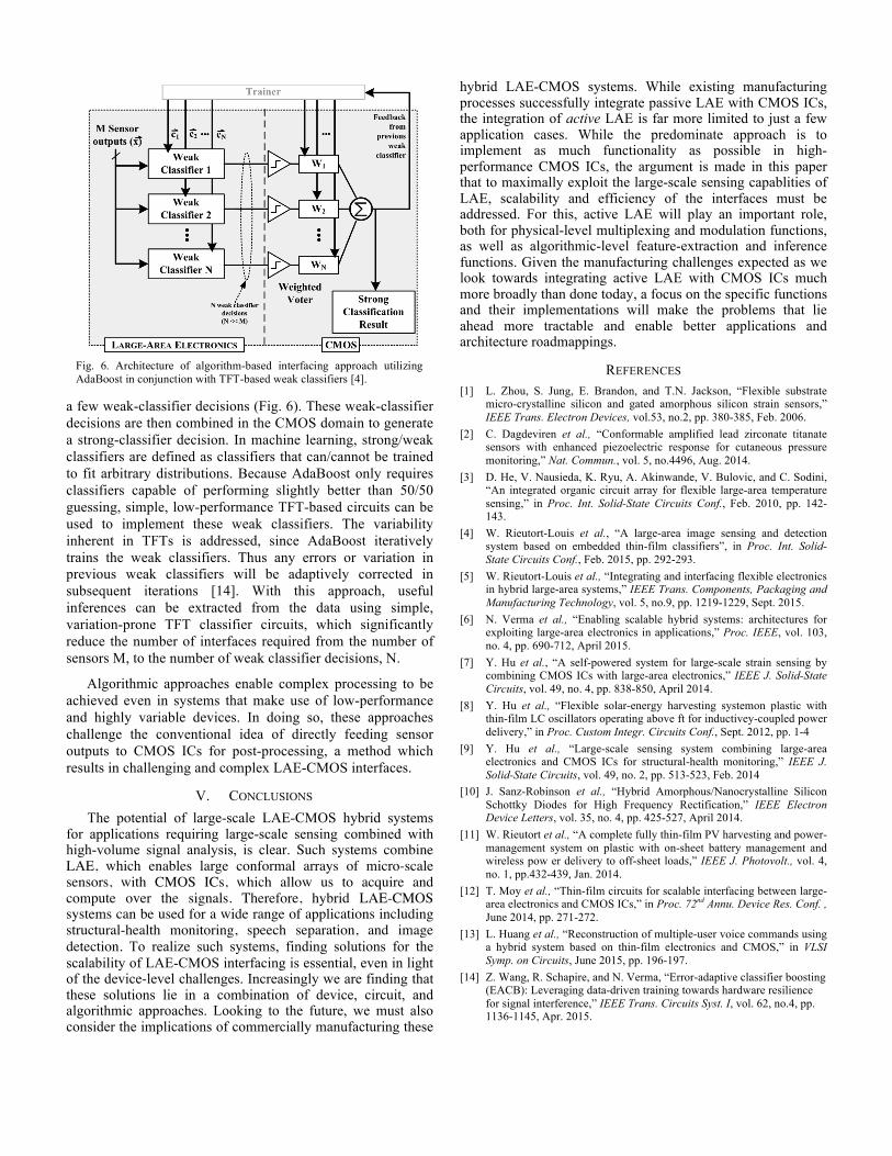
Fig. 6. Architecture of algorithm-based interfacing approach utilizing AdaBoost in conjunction with TFT-based weak classifiers [4].
a few weak-classifier decisions (Fig. 6). These weak-classifier decisions are then combined in the CMOS domain to generate a strong-classifier decision. In machine learning, strong/weak classifiers are defined as classifiers that can/cannot be trained to fit arbitrary distributions. Because AdaBoost only requires classifiers capable of performing slightly better than 50/50 guessing, simple, low-performance TFT-based circuits can be used to implement these weak classifiers. The variability inherent in TFTs is addressed, since AdaBoost iteratively trains the weak classifiers. Thus any errors or variation in previous weak classifiers will be adaptively corrected in subsequent iterations [14]. With this approach, useful inferences can be extracted from the data using simple, variation-prone TFT classifier circuits, which significantly reduce the number of interfaces required from the number of sensors M, to the number of weak classifier decisions, N.
Algorithmic approaches enable complex processing to be achieved even in systems that make use of low-performance and highly variable devices. In doing so, these approaches challenge the conventional idea of directly feeding sensor outputs to CMOS ICs for post-processing, a method which results in challenging and complex LAE-CMOS interfaces.
V. CONCLUSIONS The potential of large-scale LAE-CMOS hybrid systems
for applications requiring large-scale sensing combined with high-volume signal analysis, is clear. Such systems combine LAE, which enables large conformal arrays of micro-scale sensors, with CMOS ICs, which allow us to acquire and compute over the signals. Therefore, hybrid LAE-CMOS systems can be used for a wide range of applications including structural-health monitoring, speech separation, and image detection. To realize such systems, finding solutions for the scalability of LAE-CMOS interfacing is essential, even in light of the device-level challenges. Increasingly we are finding that these solutions lie in a combination of device, circuit, and algorithmic approaches. Looking to the future, we must also consider the implications of commercially manufacturing these
hybrid LAE-CMOS systems. While existing manufacturing processes successfully integrate passive LAE with CMOS ICs, the integration of active LAE is far more limited to just a few application cases. While the predominate approach is to implement as much functionality as possible in high-performance CMOS ICs, the argument is made in this paper that to maximally exploit the large-scale sensing capablities of LAE, scalability and efficiency of the interfaces must be addressed. For this, active LAE will play an important role, both for physical-level multiplexing and modulation functions, as well as algorithmic-level feature-extraction and inference functions. Given the manufacturing challenges expected as we look towards integrating active LAE with CMOS ICs much more broadly than done today, a focus on the specific functions and their implementations will make the problems that lie ahead more tractable and enable better applications and architecture roadmappings.
REFERENCES [1] L. Zhou, S. Jung, E. Brandon, and T.N. Jackson, “Flexible substrate
micro-crystalline silicon and gated amorphous silicon strain sensors,” IEEE Trans. Electron Devices, vol.53, no.2, pp. 380-385, Feb. 2006.
[2] C. Dagdeviren et al., “Conformable amplified lead zirconate titanate sensors with enhanced piezoelectric response for cutaneous pressure monitoring,” Nat. Commun., vol. 5, no.4496, Aug. 2014.
[3] D. He, V. Nausieda, K. Ryu, A. Akinwande, V. Bulovic, and C. Sodini, “An integrated organic circuit array for flexible large-area temperature sensing,” in Proc. Int. Solid-State Circuits Conf., Feb. 2010, pp. 142-143.
[4] W. Rieutort-Louis et al., “A large-area image sensing and detection system based on embedded thin-film classifiers”, in Proc. Int. Solid-State Circuits Conf., Feb. 2015, pp. 292-293.
[5] W. Rieutort-Louis et al., “Integrating and interfacing flexible electronics in hybrid large-area systems,” IEEE Trans. Components, Packaging and Manufacturing Technology, vol. 5, no.9, pp. 1219-1229, Sept. 2015.
[6] N. Verma et al., “Enabling scalable hybrid systems: architectures for exploiting large-area electronics in applications,” Proc. IEEE, vol. 103, no. 4, pp. 690-712, April 2015.
[7] Y. Hu et al., “A self-powered system for large-scale strain sensing by combining CMOS ICs with large-area electronics,” IEEE J. Solid-State Circuits, vol. 49, no. 4, pp. 838-850, April 2014.
[8] Y. Hu et al., “Flexible solar-energy harvesting systemon plastic with thin-film LC oscillators operating above ft for inductivey-coupled power delivery,” in Proc. Custom Integr. Circuits Conf., Sept. 2012, pp. 1-4
[9] Y. Hu et al., “Large-scale sensing system combining large-area electronics and CMOS ICs for structural-health monitoring,” IEEE J. Solid-State Circuits, vol. 49, no. 2, pp. 513-523, Feb. 2014
[10] J. Sanz-Robinson et al., “Hybrid Amorphous/Nanocrystalline Silicon Schottky Diodes for High Frequency Rectification,” IEEE Electron Device Letters, vol. 35, no. 4, pp. 425-527, April 2014.
[11] W. Rieutort et al., “A complete fully thin-film PV harvesting and power-management system on plastic with on-sheet battery management and wireless pow er delivery to off-sheet loads,” IEEE J. Photovolt., vol. 4, no. 1, pp.432-439, Jan. 2014.
[12] T. Moy et al., “Thin-film circuits for scalable interfacing between large-area electronics and CMOS ICs,” in Proc. 72nd Annu. Device Res. Conf. , June 2014, pp. 271-272.
[13] L. Huang et al., “Reconstruction of multiple-user voice commands using a hybrid system based on thin-film electronics and CMOS,” in VLSI Symp. on Circuits, June 2015, pp. 196-197.
[14] Z. Wang, R. Schapire, and N. Verma, “Error-adaptive classifier boosting (EACB): Leveraging data-driven training towards hardware resilience for signal interference,” IEEE Trans. Circuits Syst. I, vol. 62, no.4, pp. 1136-1145, Apr. 2015.