Embed Size (px)
Citation preview
Hybrid Integrated DWDM Silicon Photonic Transceiver with Self-Adaptive CMOS Circuits
Chin-Hui Chen1*, Cheng Li2, Rui Bai3, Ayman Shafik2, Marco Fiorentino1, Zhen Peng1, Patrick Chiang3,4, Samuel Palermo2, and Ray Beausoleil1
1HP Labs, Hewlett-Packard Company, Palo Alto, CA, 94304, USA 2Texa A&M University, College Station, TX, 77843, USA 3Oregon State University, Corvallis, OR, 97331, USA 4Fudan University, Shanghai, China
Author e-mail address: [email protected]
Abstract: We present a DWDM silicon photonic transceiver with self-adaptive CMOS circuits. The energy efficiency is 808fJ/bit at 5Gbps for a ring-modulator based transmitter and 275fJ/bit at 8Gbps with BER<10-15 for the receiver. OCIS codes: (200.4650) Optical interconnects; (250.3140) Integrated optoelectronic circuits
1. Introduction Emerging many-core computing systems require an interconnect fabric that provides high throughput at low power with small footprint. Dense wavelength-division-multiplexed (DWDM) interconnects using nanophotonics offer orders of magnitude better bandwidth and energy efficiency than electrical interconnects [1]. In particular, hybrid integration using a 3D stacking approach enables separate optimization between the photonics and CMOS circuits.
Carrier-injection-based ring modulators [2] can be modulated by small voltage swings to achieve large modulation depths due to the large current that flows above threshold. Due to its inherently slow diffusion time, however, a pre-emphasized transmitter (Tx) driving signal is required for high-speed operation [3]. In order to match the resonance of the rings to the input channel wavelengths and compensate for any thermal sensitivity, a tuning capability is also required. Two common ways to address this issue are thermal and bias tuning. Thermal heaters can red-shift the resonance wavelength over a wide range, while bias tuning can blue-shift the wavelength with less power penalty. In a DWDM system, the signal quality may vary significantly among channels. A tunable receiver (Rx) design with minimum power consumption overhead is favorable than an overdesign that accommodates the worst case.
We respond to the aforementioned needs by implementing a custom CMOS transceiver, consisting of a pre-emphasis driver with bias tunability for the ring-modulator-based Tx, and a self-adaptive Rx with in-situ calibration that optimizes between power consumption and input sensitivity [4]. In this paper, we demonstrate a DWDM-compatible silicon photonic transceiver with 808 fJ/bit energy efficiency for a 5 Gbps Tx, and 275 fJ/bit efficiency for an 8 Gbps Rx. We believe that this work establishes a solid foundation for future DWDM 3D integration.
(a) (b) Fig. 1. Images of the hybrid integrated silicon photonic transceiver: (a) CMOS Tx circuits wirebonded to a 2.5μm ring modulator. (b) CMOS Rx circuits wirebonded to two photodiodes for the data channel and the forwarded clock channel. 2. Silicon Photonic Transceiver The ring modulator, as shown in the inset of Fig. 1(a), consists of a circular ring waveguide with a 2.5 μm radius and a straight coupling waveguide. The modulator was formed by designing a lateral p-i-n junction for carrier injection operation with a quality factor of 11,000 and an extinction ratio of 16 dB. Light was coupled in and out of the modulator by means of grating couplers.
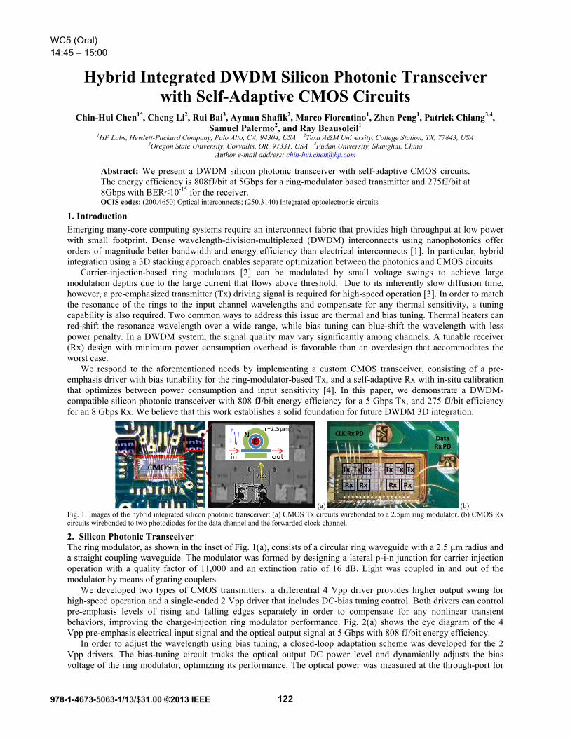
We developed two types of CMOS transmitters: a differential 4 Vpp driver provides higher output swing for high-speed operation and a single-ended 2 Vpp driver that includes DC-bias tuning control. Both drivers can control pre-emphasis levels of rising and falling edges separately in order to compensate for any nonlinear transient behaviors, improving the charge-injection ring modulator performance. Fig. 2(a) shows the eye diagram of the 4 Vpp pre-emphasis electrical input signal and the optical output signal at 5 Gbps with 808 fJ/bit energy efficiency.
In order to adjust the wavelength using bias tuning, a closed-loop adaptation scheme was developed for the 2 Vpp drivers. The bias-tuning circuit tracks the optical output DC power level and dynamically adjusts the bias voltage of the ring modulator, optimizing its performance. The optical power was measured at the through-port for
122
WC5 (Oral)14:45 – 15:00
978-1-4673-5063-1/13/$31.00 ©2013 IEEE
this demonstration, but the proposed CMOS interface can be readily integrated with the ring resonator together with a photodiode at its drop port. The resonance wavelength was blue-shifted with higher bias voltage, as shown in Fig. 2(b) and (c), because of the dominate free-carrier plasma dispersion effect. The maximum wavelength shift was -0.22 nm with 425 μW tuning power. This efficient bias-tuning (11.3 μW/GHz) can be combined with thermal heating to provide coarse and fine tuning, as well as red and blue shift in wavelength rendering a minimum overall tuning power consumption. Fig. 2(d) shows the optical eye diagram before and after bias tuning. An on-off extinction ratio of 11 dB was achieved at 500 Mbps with 2 Vpp. The measured data rate for the optical signal is limited by the large series resistance (~3kΩ) of the current ring device, due to inadequate contacts as well as long bonding wires (~1mm). The CMOS Tx was electrically verified up to 9 Gbps. For the proposed 2 Vpp Tx, bias-tuning exhibits a cost of 12% power overhead of the entire Tx power consumption.
(a) (b) (c) (d) Fig. 2. Silicon photonic Tx performance: (a) Electrical and optical eye diagrams at 5 Gbps with pre-emphasis using the 4Vpp driver. (b) Optical transmission spectra for various bias voltages. (c) Resonance wavelength shift in relation to applied bias voltage. (d) Optical eye diagrams at 500 Mbps before and after bias-tuning stabilization using the 2Vpp driver.
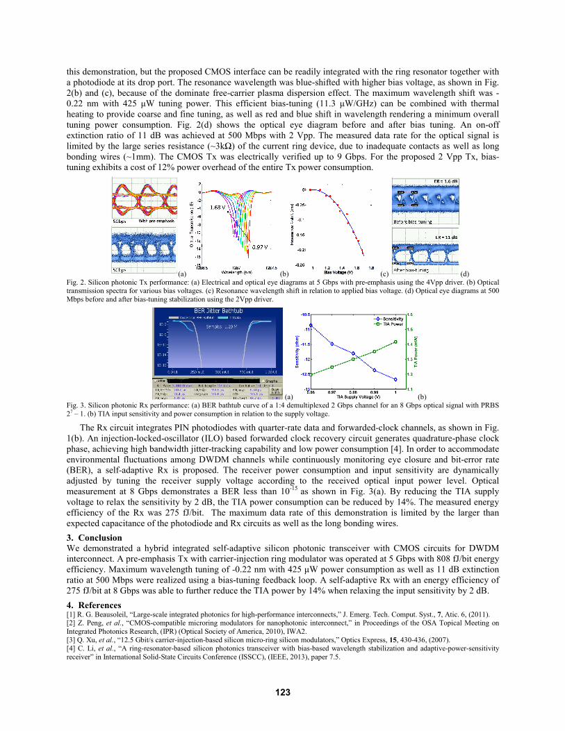
(a) (b) Fig. 3. Silicon photonic Rx performance: (a) BER bathtub curve of a 1:4 demultiplexed 2 Gbps channel for an 8 Gbps optical signal with PRBS 27 – 1. (b) TIA input sensitivity and power consumption in relation to the supply voltage.
The Rx circuit integrates PIN photodiodes with quarter-rate data and forwarded-clock channels, as shown in Fig. 1(b). An injection-locked-oscillator (ILO) based forwarded clock recovery circuit generates quadrature-phase clock phase, achieving high bandwidth jitter-tracking capability and low power consumption [4]. In order to accommodate environmental fluctuations among DWDM channels while continuously monitoring eye closure and bit-error rate (BER), a self-adaptive Rx is proposed. The receiver power consumption and input sensitivity are dynamically adjusted by tuning the receiver supply voltage according to the received optical input power level. Optical measurement at 8 Gbps demonstrates a BER less than 10-15 as shown in Fig. 3(a). By reducing the TIA supply voltage to relax the sensitivity by 2 dB, the TIA power consumption can be reduced by 14%. The measured energy efficiency of the Rx was 275 fJ/bit. The maximum data rate of this demonstration is limited by the larger than expected capacitance of the photodiode and Rx circuits as well as the long bonding wires. 3. Conclusion We demonstrated a hybrid integrated self-adaptive silicon photonic transceiver with CMOS circuits for DWDM interconnect. A pre-emphasis Tx with carrier-injection ring modulator was operated at 5 Gbps with 808 fJ/bit energy efficiency. Maximum wavelength tuning of -0.22 nm with 425 μW power consumption as well as 11 dB extinction ratio at 500 Mbps were realized using a bias-tuning feedback loop. A self-adaptive Rx with an energy efficiency of 275 fJ/bit at 8 Gbps was able to further reduce the TIA power by 14% when relaxing the input sensitivity by 2 dB. 4. References [1] R. G. Beausoleil, “Large-scale integrated photonics for high-performance interconnects,” J. Emerg. Tech. Comput. Syst., 7, Atic. 6, (2011). [2] Z. Peng, et al., “CMOS-compatible microring modulators for nanophotonic interconnect,” in Proceedings of the OSA Topical Meeting on Integrated Photonics Research, (IPR) (Optical Society of America, 2010), IWA2. [3] Q. Xu, et al., “12.5 Gbit/s carrier-injection-based silicon micro-ring silicon modulators,” Optics Express, 15, 430-436, (2007). [4] C. Li, et al., “A ring-resonator-based silicon photonics transceiver with bias-based wavelength stabilization and adaptive-power-sensitivity receiver” in International Solid-State Circuits Conference (ISSCC), (IEEE, 2013), paper 7.5.
123