Embed Size (px)
Citation preview
Hybrid fluorescent layer emitting polarized lightMohammad Mohammadimasoudi, Jeroen Beeckman, Zeger Hens, and Kristiaan Neyts
Citation: APL Materials 5, 076104 (2017); doi: 10.1063/1.4991029View online: http://dx.doi.org/10.1063/1.4991029View Table of Contents: http://aip.scitation.org/toc/apm/5/7Published by the American Institute of Physics

APL MATERIALS 5, 076104 (2017)
Hybrid fluorescent layer emitting polarized lightMohammad Mohammadimasoudi,1,2,a,b Jeroen Beeckman,1,2
Zeger Hens,2,3 and Kristiaan Neyts1,2,b1ELIS Department, Ghent University, Gent 9052, Belgium2Center for Nano- and Bio-photonics, Ghent University, Gent 9052, Belgium3Physics and Chemistry of Nanostructures, Ghent University, Gent 9000, Belgium
(Received 3 May 2017; accepted 19 June 2017; published online 18 July 2017)
Semiconductor nanorods have anisotropic absorption and emission properties. In thiswork a hybrid luminescent layer is produced based on a mixture of CdSe/CdS nanorodsdispersed in a liquid crystal that is aligned by an electric field and polymerized byUV illumination. The film emits light with polarization ratio 0.6 (polarization contrast4:1). Clusters of nanorods in liquid crystal can be avoided by applying an AC electricfield with sufficient amplitude. This method can be made compatible with large-scaleprocessing on flexible transparent substrates. Thin polarized light emitters can be usedin LCD backlights or solar concentrators to increase the efficiency. © 2017 Author(s).All article content, except where otherwise noted, is licensed under a CreativeCommons Attribution (CC BY) license (http://creativecommons.org/licenses/by/4.0/).[http://dx.doi.org/10.1063/1.4991029]
Semiconductor nanorods (NRs) have a needle-like structure and their light absorption and emis-sion properties are anisotropic.1–4 Aligning nanorods collectively along a preferred axis is attractivefor photovoltaic energy conversion, light-emitting devices, optical sensors, or switches.5–9 Severaltechniques for aligning NRs have been explored and it was found that electric-field-driven deposi-tion from a colloidal suspension is efficient for many kinds of anisotropic particles: nanowires,10
carbon nanotubes,11 gold NRs,12,13 and semiconductor NRs.3,6,14–16 Zonghai et al. reported on thealignment of CdSe and CdTe NRs along the applied electric field and the accumulation of NRs nearthe electrodes after drop-casting from a solution.17 Ryan et al. used a combination of a DC electricfield and the slow evaporation of toluene to generate superlattices of semiconductor nanorods withorientation perpendicular to the substrate.18
In these papers, good alignment is obtained, but the methods are not always compatible withcheap, reproducible, and homogeneous deposition on large substrates as required for large size appli-cations such as solar cells or OLEDs. In previous work, we presented a novel technique for thehomogeneous deposition and efficient alignment of CdSe/CdS NRs on a glass substrate which isbased on applying an electric field between electrodes during dip-coating.19,20 In this approach, thealignment of the NRs requires electric fields with amplitude up to 20 V/µm, and alignment is onlypossible on substrates with appropriately patterned electrodes. An alternative, electrode-independentapproach involves the formation of films made of aligned polyvinylpyrrolidone nanofibers, containingsilica-coated CdSe/CdS NRs oriented parallel to the nanofiber axis, with polarization ratio 0.45.21
Liquid crystals (LCs) combine properties such as long-range orientational order and optical andelectrical anisotropy while remaining fluid. The self-organizing nature of LCs has been demonstratedin different configurations22,23 and proved to be instrumental in the alignment of anisotropic objectssuch as nanowires, nanotubes,20 and metallic22 and semiconducting24 nanorods. Hybrid materialscombining different types of building blocks may display interesting properties that can be used innovel applications. Unfortunately, it is very difficult to disperse high concentrations of nanoparticlesin anisotropic fluids without the problem of aggregation. For example, the work of Tao Du et al.24,25
in which photo-alignment is used to align NRs in LC, mentions the presence of clusters of NRs in
aThis research was performed while M. Mohammadimasoudi was at ELIS, UGent, Belgium.bElectronic addresses: [email protected] and [email protected]
2166-532X/2017/5(7)/076104/6 5, 076104-1 © Author(s) 2017
076104-2 Mohammadimasoudi et al. APL Mater. 5, 076104 (2017)
LCs. Often surfactant stabilization is applied to reduce clustering as, e.g., for the case of gold NRsin lyotropic LC.22,23,26
In this work, we show that the application of an AC electric field can effectively disperse existingclusters of CdSe/CdS NRs in the nematic LC mixture. In addition, by mixing NRs into reactivemesogens instead of regular LC, the configuration of aligned nanorods in LC without aggregationscan be fixed by UV polymerization. The resulting polymer film can be detached from the ITO-coatedsubstrates. When illuminated with unpolarized blue light, it emits mainly linearly polarized greenlight by photoluminescence, with polarization contrast ratio 0.60 (intensity ratio 4:1).
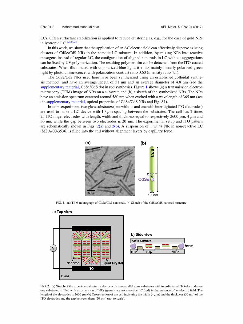
The CdSe/CdS NRs used here have been synthesized using an established colloidal synthe-sis method3 and have an average length of 51 nm and an average diameter of 4.8 nm (see thesupplementary material, CdSe/CdS dot in rod synthesis). Figure 1 shows (a) a transmission electronmicroscopy (TEM) image of NRs on a substrate and (b) a sketch of the synthesized NRs. The NRshave an emission spectrum centered around 580 nm when excited with a wavelength of 365 nm (seethe supplementary material, optical properties of CdSe/CdS NRs and Fig. S1).
In a first experiment, two glass substrates (one without and one with interdigitated ITO electrodes)are used to make a LC device with 10 µm spacing between the substrates. The cell has 2 times25 ITO finger electrodes with length, width and thickness equal to respectively 2600 µm, 4 µm and30 nm, while the gap between two electrodes is 20 µm. The experimental setup and ITO patternare schematically shown in Figs. 2(a) and 2(b). A suspension of 1 wt. % NR in non-reactive LC(MDA-00-3536) is filled into the cell without alignment layers by capillary force.
FIG. 1. (a) TEM micrograph of CdSe/CdS nanorods. (b) Sketch of the CdSe/CdS nanorod structure.
FIG. 2. (a) Sketch of the experimental setup: a device with two parallel glass substrates with interdigitated ITO electrodes onone substrate, is filled with a suspension of NRs (green) in a non-reactive LC (red) in the presence of an electric field. Thelength of the electrodes is 2600 µm (b) Cross-section of the cell indicating the width (4 µm) and the thickness (30 nm) of theITO electrodes and the gap between them (20 µm) (not to scale).
076104-3 Mohammadimasoudi et al. APL Mater. 5, 076104 (2017)
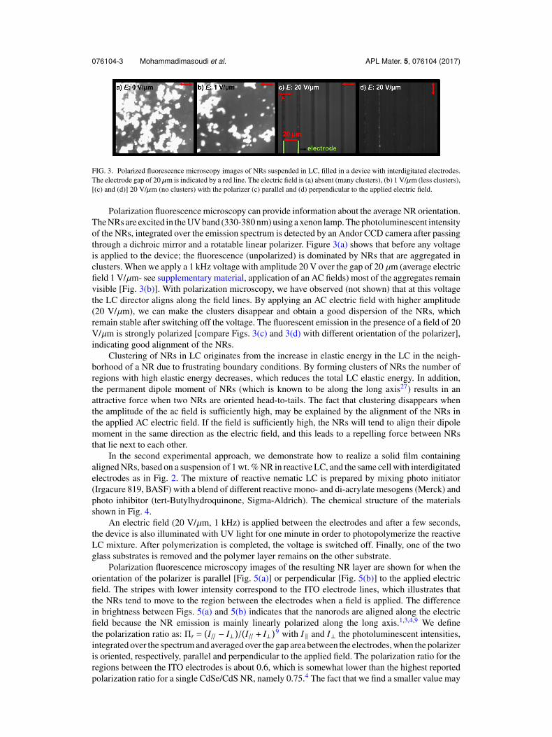
FIG. 3. Polarized fluorescence microscopy images of NRs suspended in LC, filled in a device with interdigitated electrodes.The electrode gap of 20 µm is indicated by a red line. The electric field is (a) absent (many clusters), (b) 1 V/µm (less clusters),[(c) and (d)] 20 V/µm (no clusters) with the polarizer (c) parallel and (d) perpendicular to the applied electric field.
Polarization fluorescence microscopy can provide information about the average NR orientation.The NRs are excited in the UV band (330-380 nm) using a xenon lamp. The photoluminescent intensityof the NRs, integrated over the emission spectrum is detected by an Andor CCD camera after passingthrough a dichroic mirror and a rotatable linear polarizer. Figure 3(a) shows that before any voltageis applied to the device; the fluorescence (unpolarized) is dominated by NRs that are aggregated inclusters. When we apply a 1 kHz voltage with amplitude 20 V over the gap of 20 µm (average electricfield 1 V/µm- see supplementary material, application of an AC fields) most of the aggregates remainvisible [Fig. 3(b)]. With polarization microscopy, we have observed (not shown) that at this voltagethe LC director aligns along the field lines. By applying an AC electric field with higher amplitude(20 V/µm), we can make the clusters disappear and obtain a good dispersion of the NRs, whichremain stable after switching off the voltage. The fluorescent emission in the presence of a field of 20V/µm is strongly polarized [compare Figs. 3(c) and 3(d) with different orientation of the polarizer],indicating good alignment of the NRs.
Clustering of NRs in LC originates from the increase in elastic energy in the LC in the neigh-borhood of a NR due to frustrating boundary conditions. By forming clusters of NRs the number ofregions with high elastic energy decreases, which reduces the total LC elastic energy. In addition,the permanent dipole moment of NRs (which is known to be along the long axis27) results in anattractive force when two NRs are oriented head-to-tails. The fact that clustering disappears whenthe amplitude of the ac field is sufficiently high, may be explained by the alignment of the NRs inthe applied AC electric field. If the field is sufficiently high, the NRs will tend to align their dipolemoment in the same direction as the electric field, and this leads to a repelling force between NRsthat lie next to each other.
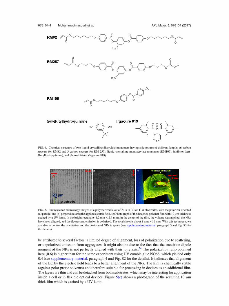
In the second experimental approach, we demonstrate how to realize a solid film containingaligned NRs, based on a suspension of 1 wt. % NR in reactive LC, and the same cell with interdigitatedelectrodes as in Fig. 2. The mixture of reactive nematic LC is prepared by mixing photo initiator(Irgacure 819, BASF) with a blend of different reactive mono- and di-acrylate mesogens (Merck) andphoto inhibitor (tert-Butylhydroquinone, Sigma-Aldrich). The chemical structure of the materialsshown in Fig. 4.
An electric field (20 V/µm, 1 kHz) is applied between the electrodes and after a few seconds,the device is also illuminated with UV light for one minute in order to photopolymerize the reactiveLC mixture. After polymerization is completed, the voltage is switched off. Finally, one of the twoglass substrates is removed and the polymer layer remains on the other substrate.
Polarization fluorescence microscopy images of the resulting NR layer are shown for when theorientation of the polarizer is parallel [Fig. 5(a)] or perpendicular [Fig. 5(b)] to the applied electricfield. The stripes with lower intensity correspond to the ITO electrode lines, which illustrates thatthe NRs tend to move to the region between the electrodes when a field is applied. The differencein brightness between Figs. 5(a) and 5(b) indicates that the nanorods are aligned along the electricfield because the NR emission is mainly linearly polarized along the long axis.1,3,4,9 We definethe polarization ratio as: Πr =
(I// − I⊥
)/(I// + I⊥
)9 with I ‖ and I⊥ the photoluminescent intensities,integrated over the spectrum and averaged over the gap area between the electrodes, when the polarizeris oriented, respectively, parallel and perpendicular to the applied field. The polarization ratio for theregions between the ITO electrodes is about 0.6, which is somewhat lower than the highest reportedpolarization ratio for a single CdSe/CdS NR, namely 0.75.4 The fact that we find a smaller value may
076104-4 Mohammadimasoudi et al. APL Mater. 5, 076104 (2017)
FIG. 4. Chemical structure of two liquid crystalline diacrylate monomers having side groups of different lengths (6-carbonspacers for RM82 and 3-carbon spacers for RM-257), liquid crystalline monoacrylate monomer (RM105), inhibitor (tert-Butylhydroquinone), and photo-initiator (Irgacure 819).
FIG. 5. Fluorescence microscopy images of a polymerized layer of NRs in LC on ITO electrodes, with the polarizer oriented(a) parallel and (b) perpendicular to the applied electric field. (c) Photograph of the detached polymer film with 10 µm thicknessexcited by a UV lamp. In the bright rectangle (1.2 mm × 2.6 mm), in the center of the film, the voltage was applied, the NRshave been aligned, and the fluorescent emission is polarized. The total sheet is about 8 mm × 16 mm. With this technique, weare able to control the orientation and the position of NRs in space (see supplementary material, paragraph 5 and Fig. S3 forthe details).
be attributed to several factors: a limited degree of alignment, loss of polarization due to scattering,or unpolarized emission from aggregates. It might also be due to the fact that the transition dipolemoment of the NRs is not perfectly aligned with their long axis.24 The polarization ratio obtainedhere (0.6) is higher than for the same experiment using UV curable glue NO68, which yielded only0.4 (see supplementary material, paragraph 4 and Fig. S2 for the details). It indicates that alignmentof the LC by the electric field leads to a better alignment of the NRs. The film is chemically stable(against polar protic solvents) and therefore suitable for processing in devices as an additional film.The layers are thin and can be detached from both substrates, which may be interesting for applicationinside a cell or in flexible optical devices. Figure 5(c) shows a photograph of the resulting 10 µmthick film which is excited by a UV lamp.

076104-5 Mohammadimasoudi et al. APL Mater. 5, 076104 (2017)
FIG. 6. Polarized fluorescence microscopy images of NRs in LC close to the edge of the electrode area while the polarizer isoriented (a) perpendicularly and (b) parallel to the line electrodes. The voltage amplitude during polymerization was 400 V,with the frequency 1 kHz.
Figure 6 shows fluorescence microscopy images of aligned NRs close to the end of the inter-digitated finger electrodes. The polarizer is oriented parallel [Fig. 6(a)] or perpendicular [Fig. 6(b)]to the applied electric field between the electrodes. The intensity differences between Figs. 6(a) and6(b) indicate that the NRs are aligned along the electric field lines, as illustrated in Fig. 2(a). Awayfrom the end of the electrode lines, where the field lines are spread out, the electric field becomesweaker, but according to the images in Fig. 6, the NRs are still well aligned.
We have demonstrated the realization of a thin film polarized emitter with polarization ratio of0.60 based on the alignment of CdSe/CdS NRs in LC. The NRs are aligned by an electric field betweenthe interdigitated electrodes and the mixture is polymerized by UV illumination. This method has thepotential to be compatible with large-scale processing on cheap, flexible, and transparent substratesand could be realized in a roll-to-roll process. The polarization ratio of the mixture of NR and reactiveLC is higher than the mixture of NR and UV curable glue. The fact that this value is much higher isascribed to the elastic coupling between NRs and LC and the collaborative effect of torques actingon the NRs and on the LC. We observe that the application of an AC electric field with amplitudeabove a few V/µm dramatically reduces clustering of NRs in LC.
See supplementary material for the additional information (CdSe/CdS dot in rod synthesis,optical properties of CdSe/CdS NRs, application of an AC fields, aligned NRs in polymer, controlthe position, and orientation of NRs and Figs. S1–S3) which is noted in the text. This material isavailable free of charge via the Internet.
This research was supported by the Interuniversity Attraction Poles program of the BelgianScience Policy Office, Under Grant No. IAP P7-35 and by the IWT-SBO project SECONDOS.
1 H. Liangtao, L. Liang-Shi, Y. Weidong, L. Manna, W. Lin-Wang, and A. P. Alivisatos, Science 292(5524), 2060–2063(2001).
2 F. Pisanello, L. Martiradonna, G. Lemeacutenager, P. Spinicelli, A. Fiore, L. Manna, J. P. Hermier, R. Cingolani, E. Giacobino,M. De Vittorio, and A. Bramati, Appl. Phys. Lett. 96(3), 033101 (2010).
3 L. Carbone, C. Nobile, M. De Giorgi, F. D. Sala, G. Morello, P. Pompa, M. Hytch, E. Snoeck, A. Fiore, I. R. Franchini,M. Nadasan, A. F. Silvestre, L. Chiodo, S. Kudera, R. Cingolani, R. Krahne, and L. Manna, Nano Lett. 7(10), 2942–2950(2007).
4 F. Pisanello, L. Martiradonna, P. Spinicelli, A. Fiore, J. P. Hermier, L. Manna, R. Cingolani, E. Giacobino, A. Bramati,M. De Vittorio, and IEEE, Polarized Single Photon Emission for Quantum Cryptography Based on Colloidal Nanocrystals(IEEE, New York, 2009).
5 M. Fisher, M. Zanella, D. J. Farrell, L. Manna, P. Stavrinou, and A. J. Chatten, “Luminescent solar concentrators utilisingaligned CdSe/CdS nanorods,” in 2011 37th IEEE Photovoltaic Specialists Conference (IEEE, Seattle, WA, 2011),pp. 000858–000863.
6 C. Nobile, V. A. Fonoberov, S. Kudera, A. Della Torre, A. Ruffino, G. Chilla, T. Kipp, D. Heitmann, L. Manna, R. Cingolani,A. A. Balandin, and R. Krahne, Nano Lett. 7(2), 476–479 (2007).
7 F. Liu, J. Wang, Z. Ge, K. Li, H. Ding, B. Zhang, D. Wang, and H. Yang, J. Mater. Chem. C 1(2), 216–219 (2013).8 A. Rizzo, C. Nobile, M. Mazzeo, M. De Giorgi, A. Fiore, L. Carbone, R. Cingolani, L. Manna, and G. Gigli, ACS Nano
3(6), 1506–1512 (2009).9 A. Persano, M. De Giorgi, A. Fiore, R. Cingolani, L. Manna, A. Cola, and R. Krahne, ACS Nano 4(3), 1646–1652 (2010).
10 H. E. Ruda and A. Shik, J. Appl. Phys. 109(6), 064305 (2011).11 S. Blatt, F. Hennrich, H. von Loehneysen, M. M. Kappes, A. Vijayaraghavan, and R. Krupke, Nano Lett. 7(7), 1960–1966
(2007).

076104-6 Mohammadimasoudi et al. APL Mater. 5, 076104 (2017)
12 B. M. I. van der Zande, G. J. M. Koper, and H. N. W. Lekkerkerker, J. Phys. Chem. B 103(28), 5754–5760 (1999).13 W. Ahmed, E. S. Kooij, A. van Silfhout, and B. Poelsema, Nano Lett. 9(11), 3786–3794 (2009).14 O. Harnack, C. Pacholski, H. Weller, A. Yasuda, and J. M. Wessels, Nano Lett. 3(8), 1097–1101 (2003).15 E. Rossitto, O. Lecarme, L. Latu-Romain, K. Berton, T. Pinedo-Rivera, T. Jiu, P. Reiss, and D. Peyrade, Microelectron.
Eng. 86(4-6), 828–831 (2009).16 S. Gupta, Q. Zhang, T. Emrick, and T. P. Russell, Nano Lett. 6(9), 2066–2069 (2006).17 Z. Hu, M. D. Fischbein, C. Querner, and M. Drndic, Nano Lett. 6(11), 2585–2591 (2006).18 K. M. Ryan, A. Mastroianni, K. A. Stancil, H. Liu, and A. P. Alivisatos, Nano Lett. 6(7), 1479–1482 (2006).19 M. Mohammadimasoudi, L. Penninck, T. Aubert, R. Gomes, Z. Hens, F. Strubbe, and K. Neyts, Opt. Mater. Express 3(12),
2045–2054 (2013).20 D. Vijayaraghavan, J. Mol. Liq. 199, 128–132 (2014).21 J. De Smet, A. Avci, P. Joshi, D. Schaubroeck, D. Cuypers, and H. De Smet, J. Soc. Inf. Disp. 21(9), 399–406 (2013).22 Y. J. Bae, H. J. Yang, S. H. Shin, K. U. Jeong, and M. H. Lee, J. Mater. Chem. 21(7), 2074–2077 (2011).23 J. Lub, D. J. Broer, R. T. Wegh, E. Peeters, and B. M. I. van der Zande, Mol. Cryst. Liq. Cryst. 429, 77 (2005).24 T. Du, J. Schneider, A. K. Srivastava, A. S. Susha, V. G. Chigrinov, H. S. Kwok, and A. L. Rogach, ACS Nano 9(11),
11049–11055 (2015).25 J. Schneider, W. Zhang, A. K. Srivastava, V. G. Chigrinov, H. S. Kwok, and A. L. Rogach, Nano Lett. 17(5), 3133–3138
(2017).26 Z. Luo, Y.-W. Cheng, and S.-T. Wu, J. Disp. Technol. 10(3), 208–214 (2014).27 M. Mohammadimasoudi, Z. Hens, and K. Neyts, RSC Adv. 6(61), 55736–55744 (2016).