Embed Size (px)
Citation preview

2019 Microchip Technology Inc. DS20006234A-page 1
HV265
Features
• Four Independent High Voltage Amplifiers
• Up to +205 V Output Voltage
• Gain of 82 V/V with Internal Feedback Resistors
• 0.02 V/s Minimum Output Slew Rate
• Less than 10 ms Settling Time
• Less than 1 k Output Impedance
• Up to 200 pF Output Load
• 30 kHz Gain Bandwidth Product
• 24-lead TSSOP Package
Application
• MEMS Driver
General Description
The HV265 device is a 4-channel high-voltageoperational amplifier array with an optional internalfeedback resistor network.
The amplifier array IC operates on a 225 V high-voltagesupply and a 5 V low-voltage supply. Each channel hasits independent input and output ports. When theinternal feedback resistor network is used, the closed-loop gain is set to 82 V/V. High value SiCr resistors areused for internal feedback networks to minimize thepower consumption. The input accepts voltage in therange of 0.05V and 2.5V.
The output impedance of the amplifier is less than 1 kand the output can drive a capacitive load up to 200 pF.The amplifier is designed to have good temperaturestability and low output drift.
Typical Application Circuit
4-Channel, 205V, High-Voltage Amplifiers Array

HV265
DS20006234A-page 2 2019 Microchip Technology Inc.
Package Types (Top View)
Block Diagram
HV26524-Lead TSSOP
See Table 2-1.

2019 Microchip Technology Inc. DS20006234A-page 3
HV265
NOTES:

HV265
DS20006234A-page 4 2019 Microchip Technology Inc.
1.0 ELECTRICAL CHARACTERISTICS
Absolute Maximum Ratings †
Low supply voltage (VDD)............................................................................................................................. -0.5V to 6.5VHigh supply voltage (VPP) ........................................................................................................................... -0.5V to 250VInput analog voltage (VIN) ............................................................................................................................ - 0.3V to VDDMaximum junction temperature ............................................................................................................................+125°CStorage temperature ...............................................................................................................................-65°C to +150°CESD Rating low voltage pins .................................................................2 kV HBM, 500 V CDM, 750 V CDM corner leadESD Rating high voltage pins............................................................. 500 V HBM, 500 V CDM, 750 V CDM corner lead
† Notice: Stresses above those listed under “Maximum Ratings” may cause permanent damage to the device. This isa stress rating only and functional operation of the device at those or any other conditions above those indicated in theoperational sections of this specification is not intended. Exposure to maximum rating conditions for extended periodsmay affect device reliability.
TABLE 1-1: OPERATING SUPPLY VOLTAGES
Electrical Specifications: Unless otherwise specified: TA = +25°C. Boldface specifications apply over the TA range of -40 to +85°C.
Parameter Sym. Min. Typ. Max. Units Conditions
High Voltage Supply VPP 50 — 225 V Note 1
Low Voltage Supply VDD 4.5 5.0 5.5 V
Note 1: Specification is obtained by characterization and is not 100% tested.
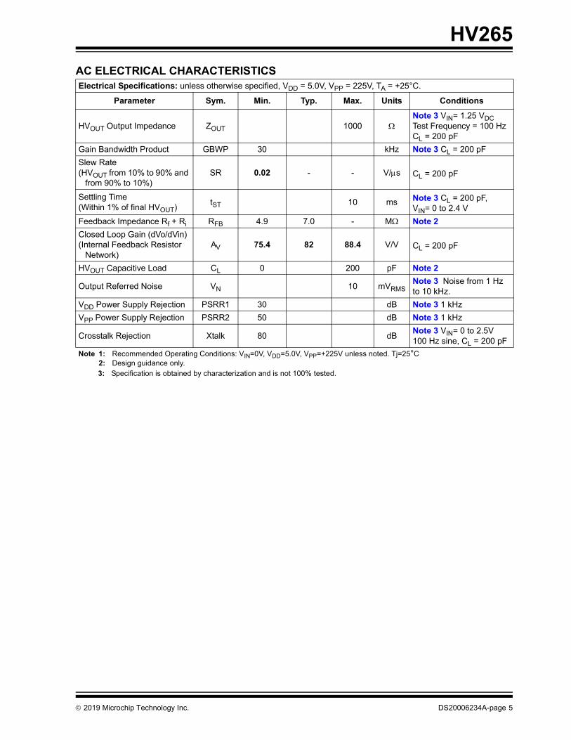
ELECTRICAL CHARACTERISTICSElectrical Specifications: unless otherwise specified, VDD = 5.0V, VPP = 225V, TA = +25°C.
Parameter Sym. Min. Typ. Max. Units Conditions
Input Ground Range RGND 0 0 VDD V
Input Analog Voltage VIN 0 — 3.3 V
Quiescent VPP Supply Current IPPQ — 300 500 µA VIN = 0 or 5V
Quiescent VDD Supply Current IDDQ — 3 5 mA VIN= 0 or 5V
VPP Supply Current IPP— — 500 µA VIN= 2VP-P 100 Hz sine,
CL = 200 pF
VDD Supply Current IDD— — 5 mA VIN= 2VP-P 100 Hz sine,
CL = 200 pF
HVOUT Output Voltage Range HVOUT 1.85 VPP - 10 V CL = 200 pF
HVOUT Sink Current ISINK 3 mA CL = 200 pF
HVOUT Source Current ISOURCE 3 mA CL = 200 pF
HVOUT High Level Output VOH 204.8 V CL = 200 pF, VIN= 2.7V
HVOUT Input DC Offset HVOS ±16 mV Note 3 CL = 200 pF
HVOUT Drift Over Time(Room Temperature)
Drift ±30 mVNote 3 CL = 200 pF, VIN= 2.5V
HVOUT Temperature Coefficient(Drift Over Temperature)
Temp. ±115 mVNote 3 CL = 200 pF, VIN= 2.5VTJ = -40°C to 85°C
Note 1: Recommended Operating Conditions: VIN=0V, VDD=5.0V, VPP=+225V unless noted. Tj=25°C2: Design guidance only.3: Specification is obtained by characterization and is not 100% tested.
2019 Microchip Technology Inc. DS20006234A-page 5
HV265
AC ELECTRICAL CHARACTERISTICSElectrical Specifications: unless otherwise specified, VDD = 5.0V, VPP = 225V, TA = +25°C.
Parameter Sym. Min. Typ. Max. Units Conditions
HVOUT Output Impedance ZOUT 1000 Note 3 VIN= 1.25 VDC Test Frequency = 100 Hz CL = 200 pF
Gain Bandwidth Product GBWP 30 kHz Note 3 CL = 200 pF
Slew Rate(HVOUT from 10% to 90% and
from 90% to 10%)SR 0.02 - - V/s CL = 200 pF
Settling Time(Within 1% of final HVOUT)
tST 10 ms Note 3 CL = 200 pF,VIN= 0 to 2.4 V
Feedback Impedance Rf + Ri RFB 4.9 7.0 - M Note 2
Closed Loop Gain (dVo/dVin)(Internal Feedback Resistor
Network)AV 75.4 82 88.4 V/V CL = 200 pF
HVOUT Capacitive Load CL 0 200 pF Note 2
Output Referred Noise VN 10 mVRMSNote 3 Noise from 1 Hz to 10 kHz.
VDD Power Supply Rejection PSRR1 30 dB Note 3 1 kHz
VPP Power Supply Rejection PSRR2 50 dB Note 3 1 kHz
Crosstalk Rejection Xtalk 80 dBNote 3 VIN= 0 to 2.5V 100 Hz sine, CL = 200 pF
Note 1: Recommended Operating Conditions: VIN=0V, VDD=5.0V, VPP=+225V unless noted. Tj=25°C2: Design guidance only.3: Specification is obtained by characterization and is not 100% tested.

HV265
DS20006234A-page 6 2019 Microchip Technology Inc.
TEMPERATURE SPECIFICATIONSElectrical Specifications: unless otherwise specified, VDD = 5.0V, VPP = 225V
Parameters Sym. Min. Typ. Max. Units Conditions
Temperature Ranges
Operating Junction Temperature Range TJ -40 — +85 °C
Maximum Junction Temperature TJ(MAX) — — +125 °C
Storage Temperature Range TA -65 — +150 °C
Package Thermal Resistances
Thermal Resistance, 24L-TSSOP JA — 87 — °C/W

2019 Microchip Technology Inc. DS20006234A-page 7
HV265
1.1 Typical Performance Curves
FIGURE 1-1: Typical Small-Signal Pulse Response (VIN=0.9~1.1V pulse 100 Hz. CL=200 pF).
FIGURE 1-2: Typical Large-Signal Pulse Response (VIN = 0~2V pulse 100 Hz. CL=200 pF).
FIGURE 1-3: Typical Rise Time (VIN = 0~2V Pulse 100 Hz. CL=200 pF).
FIGURE 1-4: Typical Fall Time (VIN = 0~2V Pulse 100 Hz. CL=200 pF).
FIGURE 1-5: Typical Bode Plot of Small Signal Input (VIN=100 mVp-p with 1.25 VDC).
FIGURE 1-6: Typical Crosstalk Rejection vs Frequency.
Note: The graphs and tables provided below are a statistical summary based on a limited number of samples andare provided for informational purposes only. The performance characteristics listed herein are not testedor guaranteed. In some graphs or tables, the data presented may be outside the specified operating range(e.g. outside specified power supply range) and therefore outside the warranted range.
10
15
20
25
30
35
40
45
100 1000 10000 100000 1000000
Magnitude in dB
Frequency in Hz
Typical Bode PlotVin = 0.1Vrms + 1.25VDC, CL = 220pF
65
70
75
80
85
90
95
100
105
10 100 1000 10000
Crosstalk Rejection in dB
Frequency in Hz
Crosstalk RejectionHVOUT = Full Swing, CL = 220pF

HV265
DS20006234A-page 8 2019 Microchip Technology Inc.
FIGURE 1-7: Typical Crosstalk Rejection in Time Domain (Source VIN = 0~2.5V Sine).
FIGURE 1-8: Distribution of Input Offset at TA = 25°C.
FIGURE 1-9: Distribution of Typical HVOUT Drift Over Temperature (VIN = 2.5VDC in Reference to TA = 20°C.
FIGURE 1-10: Typical HVOUT Drift Over Time. VPP=225V,VDD=5.0V,VIN=2.5V @TA=25°C.
FIGURE 1-11: Typical Power Supply Rejection from VDD vs Frequency.
FIGURE 1-12: Typical Power Supply Rejection from VPP vs Frequency.
Note: The graphs and tables provided below are a statistical summary based on a limited number of samples andare provided for informational purposes only. The performance characteristics listed herein are not testedor guaranteed. In some graphs or tables, the data presented may be outside the specified operating range(e.g. outside specified power supply range) and therefore outside the warranted range.
0
5
10
15
20
25
30
35
-15 -14 -13 -12 -11 -10 -8 -7 -6 -5 -4 -3 -2 -1 0 1 2 3 4 5 6 7 8 9 10 11 12 13 14 15
Coun
t
HVOUT Input Offset in mV
Typical Distribution of HVOUT Input Offset Voltage (HVOS) at 25 °C
-250
-200
-150
-100
-50
0
50
100
150
200
250
-50 -40 -30 -20 -10 0 10 20 30 40 50 60 70 80 90
Volta
ge in
mV
Temperature in degree C
HVOUT drift over temperature, Vin = 2.5Vwith respect to 20 degree C
-40
-30
-20
-10
0
10
20
30
0 1 2 3 4 5
Drift
(mV)
Time Duration (Hour)
Typical HVOUT Drift over Time at 25 °C(VIN=2.5V)

2019 Microchip Technology Inc. DS20006234A-page 9
HV265
NOTES:

HV265
DS20006234A-page 10 2019 Microchip Technology Inc.
2.0 PIN DESCRIPTION
The descriptions of the pins are listed in Table 2-1.
TABLE 2-1: PIN FUNCTION TABLE
Pin Number Symbol Description
1 VIN1 Amplifier Input 1
2 RGND1 Resistor Ground 1. Typically grounded.
3 GND Low Voltage Ground
4 VIN2 Amplifier Input 2
5 RGND2 Resistor Ground 2. Typically grounded.
6 VDD Positive Low Voltage Supply
7 GND Low Voltage Ground
8 VIN3 Amplifier Input 3
9 RGND3 Resistor Ground 3. Typically grounded.
10 GND Low Voltage Ground
11 VIN4 Amplifier Input 4
12 RGND4 Resistor Ground 4. Typically grounded.
13 NC No Connection
14 FB4 Feedback Input 4
15 HVOUT4 High Voltage Output 4
16 FB3 Feedback Input 3
17 HVOUT3 High Voltage Output 3
18 HVGND High Voltage Ground
19 VPP Positive High Voltage Supply
20 FB2 Feedback Input 2
21 HVOUT2 High Voltage Output 2
22 FB1 Feedback Input 1
23 HVOUT1 High Voltage Output 1
24 NC No Connection

2019 Microchip Technology Inc. DS20006234A-page 11
HV265
3.0 DEVICE DESCRIPTION
3.1 Power-On/Power-Off Sequence
The device can be damaged by an improper power-up/down sequence. The acceptable power-on/offsequences are shown in Table 3-1 and Table 3-2. The
user may add an external diode across VPP and VDDfor additional protection. The anode of the diode isconnected to VDD and the cathode is connected to VPP.Any low-current high-voltage diode such as a 1N4004is adequate.
TABLE 3-1: ACCEPTABLE POWER-ON SEQUENCES
TABLE 3-2: ACCEPTABLE POWER-OFF SEQUENCES
Option 1 Option 2
Steps Description Steps Description
1 VDD 1 VDD
2 VPP 2 Inputs
3 Inputs 3 VPP
Option 1 Option 2
Steps Description Steps Description
1 Inputs 1 VPP
2 VPP 2 Inputs
3 VDD 3 VDD

HV265
DS20006234A-page 12 2019 Microchip Technology Inc.
NOTES:

2019 Microchip Technology Inc. DS20006234A-page 13
HV265
4.0 PACKAGING INFORMATION
4.1 Package Marking Information
Legend: XX...X Product Code or Customer-specific informationY Year code (last digit of calendar year)YY Year code (last 2 digits of calendar year)WW Week code (week of January 1 is week ‘01’)NNN Alphanumeric traceability code Pb-free JEDEC designator for Matte Tin (Sn)* This package is Pb-free. The Pb-free JEDEC designator ( )
can be found on the outer packaging for this package.
Note: In the event the full Microchip part number cannot be marked on one line, it willbe carried over to the next line, thus limiting the number of availablecharacters for customer-specific information. Package may or may not includethe corporate logo.
3e
3e
24-Lead TSSOP Example
HV265
QEX l 123
1910
3eXXXXXXXX
XXXXNNN3e
YYWW

HV265
DS20006234A-page 14 2019 Microchip Technology Inc.
(DATUM B)
(DATUM A)
Microchip Technology Drawing C04-284A Sheet 1 of 2
For the most current package drawings, please see the Microchip Packaging Specification located athttp://www.microchip.com/packaging
Note:
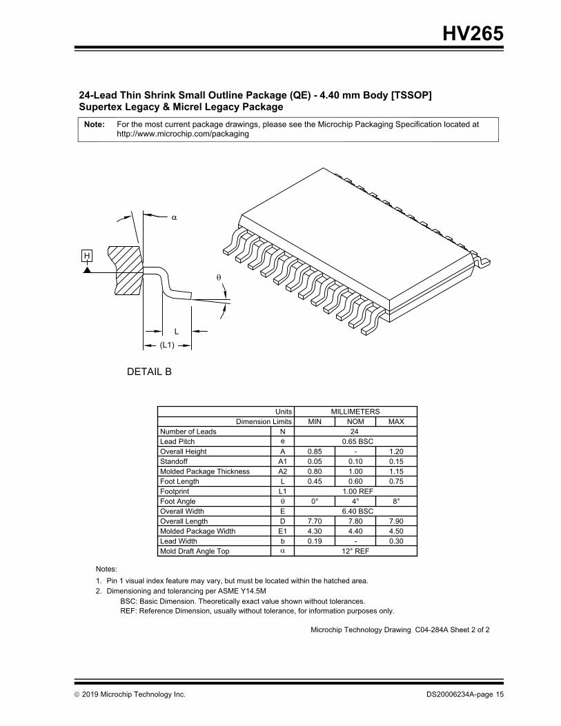
24-Lead Thin Shrink Small Outline Package (QE) - 4.40 mm Body [TSSOP]Supertex Legacy & Micrel Legacy Package
BA
2
N
TOP VIEW
SIDE VIEW
VIEW A-A
0.05 C
E
0.10 C A-B D
CSEATING
PLANE
D
A
24X b
E1
e
2X N2 TIPS
A2
A
A
SEE DETAIL BSHEET 2
0.20 C
0.10 C24X
A1
1
2019 Microchip Technology Inc. DS20006234A-page 15
HV265
Microchip Technology Drawing C04-284A Sheet 2 of 2
REF: Reference Dimension, usually without tolerance, for information purposes only.BSC: Basic Dimension. Theoretically exact value shown without tolerances.
1.2.
Notes:
Pin 1 visual index feature may vary, but must be located within the hatched area.Dimensioning and tolerancing per ASME Y14.5M
24-Lead Thin Shrink Small Outline Package (QE) - 4.40 mm Body [TSSOP]
For the most current package drawings, please see the Microchip Packaging Specification located athttp://www.microchip.com/packaging
Note:
Supertex Legacy & Micrel Legacy Package
H
L(L1)
DETAIL B
Molded Package Thickness
Dimension Limits
Mold Draft Angle Top
Foot Length
Lead WidthMolded Package WidthOverall LengthOverall WidthFoot AngleFootprint
StandoffOverall HeightLead PitchNumber of Leads
0.750.600.45L
6.40 BSC4°
1.00 REF
bE1
0.1912° REF
DE
L10°
0.30
8°
1.00
0.65 BSC24
NOMMILLIMETERS
A1A2
Ae
0.050.80
0.85
Units
NMIN
1.150.151.20
0.10-
MAX
7.907.807.704.504.404.30
-

HV265
DS20006234A-page 16 2019 Microchip Technology Inc.
Microchip Technology Drawing C04-2284A
24-Lead Thin Shrink Small Outline Package (QE) - 4.40 mm Body [TSSOP]
C
E
X1
Y1
G
BSC: Basic Dimension. Theoretically exact value shown without tolerances.
Notes:Dimensioning and tolerancing per ASME Y14.5M
For best soldering results, thermal vias, if used, should be filled or tented to avoid solder loss duringreflow process
1.
2.
For the most current package drawings, please see the Microchip Packaging Specification located athttp://www.microchip.com/packaging
Note:
Supertex Legacy & Micrel Legacy Package
RECOMMENDED LAND PATTERN
Dimension LimitsUnits
Contact Pitch
MILLIMETERS
0.65 BSCMIN
EMAX
Contact Pad Length (X24)Contact Pad Width (X24)
Y1X1
1.500.45
NOM
CContact Pad Spacing 5.80
Contact Pad to Center Pad (X20) G1 0.20
21
24
SILK SCREEN

2019 Microchip Technology Inc. DS20006234A-page 17
HV265
APPENDIX A: REVISION HISTORY
Revision A (July 2019)
• Original release of this document.

HV265
DS20006234A-page 18 2019 Microchip Technology Inc.
NOTES:

2019 Microchip Technology Inc. DS20006234A-page 19
HV265
PRODUCT IDENTIFICATION SYSTEM
To order or obtain information, e.g., on pricing or delivery, refer to the factory or the listed sales office.
PART NO. /XX
PackageDevice
Device: HV265: 4-Channel, 205V, High-Voltage Amplifiers Array
Temperature Range:
I = -40°C to +85°C
Package: QE = 24LD TSSOP 4.4mm
Example:
a) HV265-I/QE: 4-Channel 205V High-Voltage Amplifier Array, -40°C to +85°C, 24LD TSSOP package
-X
Temperature Range

HV265
DS20006234A-page 20 2019 Microchip Technology Inc.
NOTES:

2019 Microchip Technology Inc. DS20006234A-page 21
Information contained in this publication regarding deviceapplications and the like is provided only for your convenienceand may be superseded by updates. It is your responsibility toensure that your application meets with your specifications.MICROCHIP MAKES NO REPRESENTATIONS ORWARRANTIES OF ANY KIND WHETHER EXPRESS ORIMPLIED, WRITTEN OR ORAL, STATUTORY OROTHERWISE, RELATED TO THE INFORMATION,INCLUDING BUT NOT LIMITED TO ITS CONDITION,QUALITY, PERFORMANCE, MERCHANTABILITY ORFITNESS FOR PURPOSE. Microchip disclaims all liabilityarising from this information and its use. Use of Microchipdevices in life support and/or safety applications is entirely atthe buyer’s risk, and the buyer agrees to defend, indemnify andhold harmless Microchip from any and all damages, claims,suits, or expenses resulting from such use. No licenses areconveyed, implicitly or otherwise, under any Microchipintellectual property rights unless otherwise stated.
TrademarksThe Microchip name and logo, the Microchip logo, Adaptec, AnyRate, AVR, AVR logo, AVR Freaks, BesTime, BitCloud, chipKIT, chipKIT logo, CryptoMemory, CryptoRF, dsPIC, FlashFlex, flexPWR, HELDO, IGLOO, JukeBlox, KeeLoq, Kleer, LANCheck, LinkMD, maXStylus, maXTouch, MediaLB, megaAVR, Microsemi, Microsemi logo, MOST, MOST logo, MPLAB, OptoLyzer, PackeTime, PIC, picoPower, PICSTART, PIC32 logo, PolarFire, Prochip Designer, QTouch, SAM-BA, SenGenuity, SpyNIC, SST, SST Logo, SuperFlash, Symmetricom, SyncServer, Tachyon, TempTrackr, TimeSource, tinyAVR, UNI/O, Vectron, and XMEGA are registered trademarks of Microchip Technology Incorporated in the U.S.A. and other countries.
APT, ClockWorks, The Embedded Control Solutions Company, EtherSynch, FlashTec, Hyper Speed Control, HyperLight Load, IntelliMOS, Libero, motorBench, mTouch, Powermite 3, Precision Edge, ProASIC, ProASIC Plus, ProASIC Plus logo, Quiet-Wire, SmartFusion, SyncWorld, Temux, TimeCesium, TimeHub, TimePictra, TimeProvider, Vite, WinPath, and ZL are registered trademarks of Microchip Technology Incorporated in the U.S.A.
Adjacent Key Suppression, AKS, Analog-for-the-Digital Age, Any Capacitor, AnyIn, AnyOut, BlueSky, BodyCom, CodeGuard, CryptoAuthentication, CryptoAutomotive, CryptoCompanion, CryptoController, dsPICDEM, dsPICDEM.net, Dynamic Average Matching, DAM, ECAN, EtherGREEN, In-Circuit Serial Programming, ICSP, INICnet, Inter-Chip Connectivity, JitterBlocker, KleerNet, KleerNet logo, memBrain, Mindi, MiWi, MPASM, MPF, MPLAB Certified logo, MPLIB, MPLINK, MultiTRAK, NetDetach, Omniscient Code Generation, PICDEM, PICDEM.net, PICkit, PICtail, PowerSmart, PureSilicon, QMatrix, REAL ICE, Ripple Blocker, SAM-ICE, Serial Quad I/O, SMART-I.S., SQI, SuperSwitcher, SuperSwitcher II, Total Endurance, TSHARC, USBCheck, VariSense, ViewSpan, WiperLock, Wireless DNA, and ZENA are trademarks of Microchip Technology Incorporated in the U.S.A. and other countries.
SQTP is a service mark of Microchip Technology Incorporated in the U.S.A.The Adaptec logo, Frequency on Demand, Silicon Storage Technology, and Symmcom are registered trademarks of Microchip Technology Inc. in other countries.GestIC is a registered trademark of Microchip Technology Germany II GmbH & Co. KG, a subsidiary of Microchip Technology Inc., in other countries. All other trademarks mentioned herein are property of their respective companies.
© 2019, Microchip Technology Incorporated, All Rights Reserved.
ISBN: 978-1-5224-4776-4
Note the following details of the code protection feature on Microchip devices:
• Microchip products meet the specification contained in their particular Microchip Data Sheet.
• Microchip believes that its family of products is one of the most secure families of its kind on the market today, when used in the intended manner and under normal conditions.
• There are dishonest and possibly illegal methods used to breach the code protection feature. All of these methods, to our knowledge, require using the Microchip products in a manner outside the operating specifications contained in Microchip’s Data Sheets. Most likely, the person doing so is engaged in theft of intellectual property.
• Microchip is willing to work with the customer who is concerned about the integrity of their code.
• Neither Microchip nor any other semiconductor manufacturer can guarantee the security of their code. Code protection does not mean that we are guaranteeing the product as “unbreakable.”
Code protection is constantly evolving. We at Microchip are committed to continuously improving the code protection features of ourproducts. Attempts to break Microchip’s code protection feature may be a violation of the Digital Millennium Copyright Act. If such actsallow unauthorized access to your software or other copyrighted work, you may have a right to sue for relief under that Act.
For information regarding Microchip’s Quality Management Systems, please visit www.microchip.com/quality.

DS20006234A-page 22 2019 Microchip Technology Inc.
AMERICASCorporate Office2355 West Chandler Blvd.Chandler, AZ 85224-6199Tel: 480-792-7200 Fax: 480-792-7277Technical Support: http://www.microchip.com/supportWeb Address: www.microchip.com
AtlantaDuluth, GA Tel: 678-957-9614 Fax: 678-957-1455
Austin, TXTel: 512-257-3370
BostonWestborough, MA Tel: 774-760-0087 Fax: 774-760-0088
ChicagoItasca, IL Tel: 630-285-0071 Fax: 630-285-0075
DallasAddison, TX Tel: 972-818-7423 Fax: 972-818-2924
DetroitNovi, MI Tel: 248-848-4000
Houston, TX Tel: 281-894-5983
IndianapolisNoblesville, IN Tel: 317-773-8323Fax: 317-773-5453Tel: 317-536-2380
Los AngelesMission Viejo, CA Tel: 949-462-9523Fax: 949-462-9608Tel: 951-273-7800
Raleigh, NC Tel: 919-844-7510
New York, NY Tel: 631-435-6000
San Jose, CA Tel: 408-735-9110Tel: 408-436-4270
Canada - TorontoTel: 905-695-1980 Fax: 905-695-2078
ASIA/PACIFICAustralia - SydneyTel: 61-2-9868-6733
China - BeijingTel: 86-10-8569-7000
China - ChengduTel: 86-28-8665-5511
China - ChongqingTel: 86-23-8980-9588
China - DongguanTel: 86-769-8702-9880
China - GuangzhouTel: 86-20-8755-8029
China - HangzhouTel: 86-571-8792-8115
China - Hong Kong SARTel: 852-2943-5100
China - NanjingTel: 86-25-8473-2460
China - QingdaoTel: 86-532-8502-7355
China - ShanghaiTel: 86-21-3326-8000
China - ShenyangTel: 86-24-2334-2829
China - ShenzhenTel: 86-755-8864-2200
China - SuzhouTel: 86-186-6233-1526
China - WuhanTel: 86-27-5980-5300
China - XianTel: 86-29-8833-7252
China - XiamenTel: 86-592-2388138
China - ZhuhaiTel: 86-756-3210040
ASIA/PACIFICIndia - BangaloreTel: 91-80-3090-4444
India - New DelhiTel: 91-11-4160-8631
India - PuneTel: 91-20-4121-0141
Japan - OsakaTel: 81-6-6152-7160
Japan - TokyoTel: 81-3-6880- 3770
Korea - DaeguTel: 82-53-744-4301
Korea - SeoulTel: 82-2-554-7200
Malaysia - Kuala LumpurTel: 60-3-7651-7906
Malaysia - PenangTel: 60-4-227-8870
Philippines - ManilaTel: 63-2-634-9065
SingaporeTel: 65-6334-8870
Taiwan - Hsin ChuTel: 886-3-577-8366
Taiwan - KaohsiungTel: 886-7-213-7830
Taiwan - TaipeiTel: 886-2-2508-8600
Thailand - BangkokTel: 66-2-694-1351
Vietnam - Ho Chi MinhTel: 84-28-5448-2100
EUROPEAustria - WelsTel: 43-7242-2244-39Fax: 43-7242-2244-393
Denmark - CopenhagenTel: 45-4450-2828 Fax: 45-4485-2829
Finland - EspooTel: 358-9-4520-820
France - ParisTel: 33-1-69-53-63-20 Fax: 33-1-69-30-90-79
Germany - GarchingTel: 49-8931-9700
Germany - HaanTel: 49-2129-3766400
Germany - HeilbronnTel: 49-7131-72400
Germany - KarlsruheTel: 49-721-625370
Germany - MunichTel: 49-89-627-144-0 Fax: 49-89-627-144-44
Germany - RosenheimTel: 49-8031-354-560
Israel - Ra’anana Tel: 972-9-744-7705
Italy - Milan Tel: 39-0331-742611 Fax: 39-0331-466781
Italy - PadovaTel: 39-049-7625286
Netherlands - DrunenTel: 31-416-690399 Fax: 31-416-690340
Norway - TrondheimTel: 47-7288-4388
Poland - WarsawTel: 48-22-3325737
Romania - BucharestTel: 40-21-407-87-50
Spain - MadridTel: 34-91-708-08-90Fax: 34-91-708-08-91
Sweden - GothenbergTel: 46-31-704-60-40
Sweden - StockholmTel: 46-8-5090-4654
UK - WokinghamTel: 44-118-921-5800Fax: 44-118-921-5820
Worldwide Sales and Service
05/14/19

Mouser Electronics
Authorized Distributor
Click to View Pricing, Inventory, Delivery & Lifecycle Information: Microchip:
HV265-I/QE