Embed Size (px)
Citation preview

Adv. Radio Sci., 16, 109–116, 2018https://doi.org/10.5194/ars-16-109-2018© Author(s) 2018. This work is distributed underthe Creative Commons Attribution 4.0 License.
Humidity and temperature sensor system demonstrator with NFCtag for HySiF applicationsAmro Eldebiky1,2, Mourad Elsobky1, Harald Richter1, and Joachim N. Burghartz1
1Institut für Mikroelektronik Stuttgart – IMS CHIPS, Allmandring 30a, 70569 Stuttgart, Germany2German University in Cairo, 11432 Cairo, Egypt
Correspondence: Mourad Elsobky ([email protected])
Received: 27 January 2018 – Revised: 18 June 2018 – Accepted: 13 August 2018 – Published: 4 September 2018
Abstract. Hybrid System-in-Foil (HySiF) is one of theemerging branches of flexible electronics in which ultra-thinsilicon chips are integrated with flexible sensors in polymericfoils (Elsobky et al., 2018; Alavi et al., 2018). Intensive at-tention was given to the implementation of flexible environ-mental sensing platforms for logistics and food packaging(Cartasegna et al., 2011; Liu et al., 2016). The aim of thiswork is the implementation of a sensor system demonstra-tor using HySiF components, namely an ultra-thin micro-controller chip in addition to an on-chip temperature and anon-foil humidity sensors. The measurement concept for therelative humidity sensor is measuring the capacitance differ-ence between an off-chip (on the foil substrate) humidity de-pendent sensor capacitor, and another humidity independentreference capacitor. The electrical readout technique is basedon the charge amplifier switched capacitor circuit. It is imple-mented using a commercially available microcontroller (EMmicroelectronics EM6819) which has the advantage of be-ing available as single chips to enable post-processing stepssuch as backthining and chip embedding in a thin polymerpackage. Sensor and reference capacitors are homogeneouslyintegrated on-foil. 400 and 30µm thick microcontroller dies(MCU) are used in this application. The charge amplifier re-sult is digitized using an internal 10-bit analog-to-digital con-verter (ADC). The 10-bit ADC is time multiplexed betweenthe charge amplifier structure and the internal temperaturesensor. Linear interpolation is used to fit the digital outputof the ADC and calibrate the output of the sensor system.Readings of the humidity level and the temperature are writ-ten to an NFC tag (from the company EM microelectronicsbased on chip EM NF4) using the contact interface. Readingscan be accessed using a customized android application on asmartphone.
1 Introduction
Industry 4.0 is the term used to represent the fourth indus-trial revolution first proposed at Hannover fair (Zhou et al.,2015; Jazdi, 2014). Cyber-Physical System (CPS), and In-ternet of Things (IoT) represent the bases of Industry 4.0,which lead to what is known as the intelligent factory. Build-ing a highly flexible production model of personalized digi-tal products and services, with real-time interactions betweenpeople, products and devices is the main objective of Industry4.0 (Zhou et al., 2015). ParsiFAl4.0, which stands for “Pro-duktfähige autarke und sichere Foliensysteme für Automa-tisierungsösungen in Industrie 4.0”, is an Industry 4.0 re-search project, which aims to develop innovative sensor tech-nology and electronics in thin plastic films with cooperationpartners from industry and research (Parsifal 4.0., 2017). Inthis project, a demonstration of pneumatic drives and pack-aged goods can collect, evaluate and exchange informationabout the respective production process through flexible sen-sor labels. These smart labels are implemented by using flex-ible sensors and circuit elements, as well as technologicalapproaches like HySiF.
The main objective of this work is the design and imple-mentation of a sensor system demonstrator for environmen-tal quantities (humidity and temperature) using HySiF com-ponents, namely an ultra-thin microcontroller chip, on-chiptemperature, and on-foil humidity sensors. As Fig. 1 showsthe system structure, the on-foil humidity sensor is inter-faced with the ultra-thin EM6819 MCU used to implementthe readout of the humidity sensor. Measurements of the hu-midity sensor and the internal on-chip temperature sensorare written to an NFC tag accessed by an android applica-tion on a smartphone, and also sent to a PC and plotted inreal-time application. Sending the data to the PC is done us-
Published by Copernicus Publications on behalf of the URSI Landesausschuss in der Bundesrepublik Deutschland e.V.

110 A. Eldebiky et al.: Humidity and temperature sensor system demonstrator with NFC tag for HySiF applications
Figure 1. MCU based system overview: A readout technique for the sensor based on the charge amplifier circuit is implemented using theavailable resources of the EM6819 MCU, and switching techniques programmed on the MCU. The MCU processes collect readings fromthe humidity sensor, and the reading of the internal temperature sensor and sends readings to the EM NFC tag on a contact serial interface.Measurements are read from the NFC tag using an android application developed at IMS CHIPS on a smartphone. Sending the data to thePC is done using the UART interface of the PC and using the TI CC2650 MCU as a converter from SPI to UART.
ing the UART interface of the PC and using the TI CC2650MCU as a converter from SPI to UART (EM6819 MCU doesnot have a UART interface). This is a step in the process ofthe smart labels of the Parsifal 4.0 project, and on the roadof enabling flexible electronics for applications of industry4.0. The structure of the on-foil humidity sensor is explainedin Sect. 2. Additionally, Sect. 3 discusses the implementa-tion of the readout circuit using the EM6819 MCU resourcesand overviews its architecture. Section 4 discusses the char-acterization of the sensor system and results. Finally, Sect. 5concludes the main findings of this work.
2 On-foil Humidity Sensors
Humidity sensors measurement concept is generally one oftwo alternatives: either capacitive, or resistive. For the ca-pacitive approach, the relative humidity value is determinedbased on the change of the capacitance of the sensor as thedielectric constant of the sensing material is dependent on therelative humidity value.
In this work, capacitive humidity sensors are used. In ad-dition, the capacitance reading is done as a differential mea-surement between a humidity sensor capacitor, and anotherhumidity independent reference capacitor (Elsobky et al.,2017). The structure of the capacitive sensors used in thiswork is the interdigitated fingers structure (shown in Fig. 2)due to its simplicity to be integrated in our foil system (1metal layer). Different finger widths and spacings are fabri-cated and characterized ranging from 5 to 20µm with metalthickness from 2 to 5µm in a fixed area of 5mm×5mm. Theused material whose relative permittivity change with rela-tive humidity level is Durimide (Fujifilm Electronics Materi-als). The material is spin-coated on the interdigitated struc-ture of the sensor at speed of 1500 rpm, and baking temper-ature of 250 ◦C. The achieved thickness is from 2 to 5µm(Elsobky et al., 2017). The main difference between the sen-
Figure 2. On-foil interdigitated humidity sensor and reference ca-pacitor structure. Both capacitors have identical structure with thereference capacitor covered with additional BCB layer (Elsobky etal., 2017).
sor and the reference capacitors is that the reference capacitoris covered with a Benzocyclobutene (BCB) layer in order tomake it insensitive to the variation in the humidity level.
3 Microcontroller based Readout for Humidity Sensor
The implemented approach for interfacing with the flexiblecapacitive sensor is a microcontroller based readout tech-nique. The sensor readout is implemented using EM6819microcontroller resources (Operational Amplifier (Op-Amp),10-bit analog to digital converter (ADC), serial peripheralinterface (SPI), timer, interrupt request controller, and gen-eral purpose input/output pins (GPIO)) with a switchingmechanism that will be discussed in this section. The inter-nal bandgap temperature sensor is used to get the tempera-ture reading with the typical range for the operation of the
Adv. Radio Sci., 16, 109–116, 2018 www.adv-radio-sci.net/16/109/2018/

A. Eldebiky et al.: Humidity and temperature sensor system demonstrator with NFC tag for HySiF applications 111
Figure 3. (a) charge amplifier circuit. (b) EM 6819 Op-Amp con-nections overview (EM Microelectronic- Marin SA., 2014).
Table 1. EM6819 Op-Amp positive input selection.
OpAmpSelInpPos[1:0] Positive input
00 PA301 PC310 VBGR11 VVLD
EM6819 MCU is from −40 to 85 ◦C. The ADC configura-tion is time multiplexed between the charge amplifier struc-ture for the humidity reading and the temperature sensor. TheEM6819 is a microcontroller designed to be battery operatedfor extended lifetime applications. It has a large voltage rangefrom 3.6 V down to 0.9 V (3-V battery operated in this appli-cation for autonomous operation). It has an 8-bit RISC archi-tecture specially designed for very low power consumption(EM Microelectronic- Marin SA., 2014).
3.1 Charge Amplifier Circuit Structure
The readout circuit depends on the charge amplifier switchedcapacitor circuit using an Op-Amp (Fig. 3a). It measures thecapacitance difference between two capacitors connected ina half bridge configuration where the charge difference be-tween the sensor capacitor (CSensor) and the reference ca-pacitor (CRef) is sampled on the sampling capacitor (CMess).The circuit switches between two states. The first state is thereset phase, and the second one is the sampling phase. The
Table 2. EM6819 Op-Amp negative input selection.
OpAmpSelInpNeg[1:0] Negative input
00 PA201 PC210 VBGR11 VVLD
Table 3. EM6819 Op-Amp output port selection.
OpAmpSelOut Output
0 PA11 PC1
reference voltage of the charge amplifier represents the ana-log output voltage for the case of zero capacitance differencemeasured (1C = 0) (common mode voltage). The feedbackcapacitor (CMess) defines the maximum capacitance differ-ence that can be measured, and the sensitivity of the circuitto 1C. During the reset phase, no ADC conversion is runand the feedback capacitor is shorted to return to the resetphase. The analog output of the Op-Amp in this case is thecommon mode voltage connected to the positive input of theOp-Amp. When the circuit switches to the sampling phase,the analog output is connected to CMess. CMess is applied inthe feedback (no short circuit), and ADC conversion can takeplace after next toggle of Vosc+ and Vosc− to get the digitalreading. The analog output voltage is defined by:
Vout = Vref+Vsup ·CSensor−CRef
CMess(1)
3.2 EM6819 Operational Amplifier Structure
Figure 3b shows connections overview of the EM6819 Op-Amp. Each pin of the Op-Amp in EM6819 can be connectedto different GPIOs, or other peripherals of the EM6819 mi-crocontroller. These connections are programmed by ad-justing the corresponding bit in the Op-Amp configura-tion registers. The positive input selection is done withOpAmpSelInpPos[1:0] in register RegOpAmpCfg2[7:0] asshown in table 1.
The negative input selection is done withOpAmpSelInpNeg[1:0] in register RegOpAmpCfg2[7:0] asshown in Table 2.
When the Op-Amp is enabled, the output can be mappedon to different GPIOs with OpAmpSelOut in register Re-gOpAmpCfg2[3] as shown in Table 3.
www.adv-radio-sci.net/16/109/2018/ Adv. Radio Sci., 16, 109–116, 2018

112 A. Eldebiky et al.: Humidity and temperature sensor system demonstrator with NFC tag for HySiF applications
Figure 4. (a) EM6819 charge amplifier reset phase. (b) samplephase. (c) Charge amplifier reset phase mapped on EM6819 re-sources. (d) sample phase.
By comparison between the available architecture as Fig. 3shows, and the intended structure and functionality, it isachieved by dividing the problem into two phases:
1. Reset phase: Figure 4a shows the circuit structure dur-ing the reset phase and how it is mapped to EM6819resources and pin assignment in Fig. 4c:
– The feedback capacitor must be reset – its positiveterminal must be connected to virtual ground in or-der to discharge (Q= CV).
– The Op-Amp output is not connected to the ADCfor sampling (no conversion takes place), but con-nected to its negative input terminal in feedback,and the structure can be shown as in Fig. 4a.
2. Sampling phase: Figure 4b shows the circuit structureduring the sampling phase and how it is mapped toEM6819 resources and pin assignment in Fig. 4d:
– The feedback capacitor must be connected betweenthe two different terminals of the negative input,and the output of the Op-Amp.
– The Op-Amp output is no longer connected to itsnegative input, and is connected to the input of theADC (the conversion takes place after the next tog-gle).
Vosc+, and Vosc− are implemented using two GPIO pins asdigital outputs that toggle periodically based on the timer in-terrupt. The timer full value is set depending on the requiredperiod for the square wave excitation of the half bridge, sothat Vosc+, and Vosc− are 3 and 0 V alternatively with the re-quired phase shift of the 180◦. PC5 and PC6 pins are used forthis purpose, so the negative terminal of the reference capac-itor is connected to PC5 (Vosc−), and the negative terminal ofthe sensor capacitor is connected to PC6 (Vosc+). The posi-tive terminal of each capacitor needs to be connected to thenegative input of the Op-Amp. PC2 is used as the negativeinput GPIO pin of the Op-Amp (Table 2), so the positive ter-minal of the reference and the sensor are connected to PC2together.
The positive input of the Op-Amp is the common modevoltage for the amplifier circuit which is supposed to beVsup/2 for symmetric operation of the readout circuit. How-ever, in our application the internal bandgap reference volt-age (VBGR=1.236 V) is used as the common mode voltagefor the Op-Amp due to the absence of integrated Vsup/2 volt-age. This change in value of common mode from Vsup/2(1.5 V) to 1.236 V causes a shift of the mid-range result of thecapacitance difference 1C = 0, and is discussed in demon-stration and results section. These previous connections arethe same for the reset phase and the sampling phase, so noswitching occurs for these pins.
Thus, the two nodes which are switched between the twostates are the positive terminal of the feedback capacitor, and
Adv. Radio Sci., 16, 109–116, 2018 www.adv-radio-sci.net/16/109/2018/

A. Eldebiky et al.: Humidity and temperature sensor system demonstrator with NFC tag for HySiF applications 113
Figure 5. If the pin PC6 (Vosc+) is high, then the sample phasemust be applied, and wait for the next edge (toggle), and if it is low(the wait for the next toggle is over) then we start acquisition of theADC reading as explained, and accumulating the acquired readingon the sum, then the reset phase setup is applied.
the output node of the Op-Amp. In order to map these twonodes to match the available structure of the EM6819 micro-controller, the positive terminal of the feedback capacitor isconnected to two shorted GPIO pins of the microcontroller.One of them is available as the analog bandgap referencevoltage output, while the other one is available as the outputnode for the Op-Amp. After reference to Table 3 we chosePA1, and PA6 (which is available as VBGR output).
Concerning the output of the Op-Amp, after reference toTable 3, the two available options are PA1 and PC1. PA1 isavailable as ADC analog input, so it will be assigned to theOp-Amp output during sampling, and to the ADC input byadjusting the bits ADCSelSrc[2:0]. The second choice for theOp-Amp output PC1 is assigned to the Op-Amp output dur-ing the reset phase, and the GPIO pins PC1 (Op-Amp resetphase output), and PC2 (Op-Amp negative input terminal)are short circuited on hardware connection to get the shortcircuit feedback discussed above. Figure 5 shows the non-overlapping timing scheme for switching between the resetphase and the sample phase. When switching between twopins, we have to set one of them as high impedance (digitalinput), and then enable the functionality of the other, in or-der to avoid two nodes shorted on each other, and each oneis trying to drive the pin. Figure 6 shows the program flowwhich can be divided into two parts:
1. The setting of the microcontroller environment.
2. The periodic acquisition of the results, averaging anddisplaying.
This periodic part of the program is done in the contextof the interrupt request handler of the timer full value inter-rupt. The functionality of this periodic interrupt is to gather10 (programmed changeable number) digital readings of theoutput of the charge amplifier, and then send the average ofthese readings, with the current temperature reading at thistime to both: the NF4 tag (using the 3-wires contact inter-face), and the TI CC2650 microcontroller using SPI inter-face. The TI CC2650 is then used to send the received datato the PC on UART. The data is sent to the PC in this indirectway, because the EM6819 does not have a UART peripheral,
Figure 6. EM6819 program algorithm flowchart: At start of the pro-gram initial setup is done for all used peripherals, and then in everyperiodic call of the interrupt handler we check to see whether the re-quired number of capacitance difference measurements is reachedor not. If it is reached, then the average is calculated, the ADC isconfigured for initiating temperature sensor measurement, and thenboth the average of the 10-bit reading of the capacitance difference,and the temperature reading in Celsius degrees are written on theNFC tag. The average is also sent on the SPI interface. If the num-ber is not reached yet, we complete our measurements cycles.
so in order to be able to plot readings in real time and savereadings in a file on the PC, the TI CC2650 is used as a con-verter from SPI to UART. If the number was not reached yet,we complete our measurements. The PC6, and PC5 GPIOpins are toggled, and the timing diagram in Fig. 5 is followed.
www.adv-radio-sci.net/16/109/2018/ Adv. Radio Sci., 16, 109–116, 2018

114 A. Eldebiky et al.: Humidity and temperature sensor system demonstrator with NFC tag for HySiF applications
Figure 7. Capacitance readings of the sensor characterization inthe climate chamber linear fit: coefficients (with 95 % confidencebounds): p1= 1.006×10⁻¹²(7.492×10−13,1.263×10−12),p2=3.74× 10⁻¹²(−1.433× 10−11,2.181× 10−11). Goodness of fit:SSE= 4.883× 10⁻²⁴, R-square= 0.9811, Adjusted R-square=0.9748, RMSE= 1.276× 10⁻¹².
Figure 8. Near field communication (NFC) tag based on EM NF4chip, and android application developed to access readings writtento the NFC tag.
4 System Demonstrator and Results
4.1 Humidity Sensor Characterization in ControlledClimate Chamber
A controlled climate chamber (Vötsch VCL 0010) is used tovary the relative humidity level with steps of 5 % at temper-ature of 30 ◦C while the humidity capacitive sensor L10S20(interdigitated with finger width of 10µm and finger spac-ing of 20µm – area 5mm× 5mm) is placed inside it. Thesensor is connected during this experiment to the LCR meter(HEWLETT PACKARD 4284A Precision LCR Meter, 20 Hzto 1 MHz) in a four point measurement setup in order to mea-sure the capacitance with different humidity levels. As Fig. 7shows, the recorded points of measurement are then linearlyfitted in MATLAB to find a linear fit (f (x)= p1·x+p2) andcheck the goodness of this fit by calculating R-square, Rootmean squared error (RMSE), and The Sum of Squares due toError (SSE).
4.2 Graphical User Interface
In this demonstration, two methods are used in order to dis-play the obtained results of the system:
– Real-time plot of the data sent on UART to a PC usingMATLAB. The baud rate is 9600 while the delay of the
Table 4. The ADC results of the circuit characterization experiment.
Capacitance (pF) MCU 1 MCU 2 MCU 3
0 410 418 4041 432 441 4242 454 464 4403 476 487 45210 565 562 51411 574 571 52412 582 579 53420 654 649 65521 665 664 66930 799 792 81040 876 894 88447 876 894 884
update of the screen is set to 0.01 s. The program alsowrites the time and data vectors history to a file so thatit can be used for analysis.
– NFC tag based on the NF4 chip by the company EMmicroelectronics. The NFC tag is read by an androidapplication on a smartphone as shown in Fig. 8.
4.3 MCU based Readout Static Characterization
In order to characterize the performance of the charge ampli-fier structure, an experiment is conducted using discrete cir-cuit elements on a breadboard. Single capacitance measure-ment is done instead of capacitance difference measurement.The value of the capacitance is changed by connecting manydiscrete capacitors in parallel, and also changing the valuesof the connected capacitors. The value of the ADC outputwas recorded at each value of the capacitance by displayingit on the PC. Different MCUs are used in this experimentin order to notice the difference in performance between thedifferent units. The value of the feedback capacitor in thisexperiment is 47 pF. Table 4 shows the results for three dif-ferent MCUs. The MCU wafer was originally 200 mm in di-ameter. A 150 mm-diameter wafer is cut out of it after that.Next, a 10 nm-thick titanium layer is deposited by sputter-ing. The next step is deposition of a 100 nm-thick titaniumnitride layer also by sputtering. Lithography process and dryetching is then applied to the wafer. Finally, it is annealed at400 ◦C temperature in nitrogen for an hour, and for 30 min inhydrogen. The three MCUs differ in the order of processingsteps they experience. The first MCU (MCU 1) was thinnedto 400µm, and then annealed for reconstruction. The sec-ond MCU (MCU 2) was first annealed, and then thinned to400µm. The third MCU (MCU 3) was thinned to 400µm andwas not annealed.
As noticed from Table 4, the effective number of bits isreduced to about 9.78 and the mid-range (1C = 0) valueis shifted below 512 because of the usage of the internal
Adv. Radio Sci., 16, 109–116, 2018 www.adv-radio-sci.net/16/109/2018/

A. Eldebiky et al.: Humidity and temperature sensor system demonstrator with NFC tag for HySiF applications 115
Figure 9. The circuit characterization ADC result linear fitfor MCU 1: coefficients (with 95 % confidence bounds):p1= 11.53(10.65,12.41),p2= 432.5(416.3,448.6). Goodness offit: SSE= 2281, R-square= 0.9899, Adjusted R-square= 0.9887,RMSE= 15.92.
Figure 10. The circuit characterization ADC result linearfit for MCU 2: coefficients (with 95 % confidence bounds):p1= 11.47(10.76,12.17),p2= 436.5(423.4,449.5). Goodness offit: SSE= 1476, R-square= 0.9933, Adjusted R-square= 0.9926,RMSE= 12.81.
bandgap reference voltage (VBGR=1.236 V) as the commonmode voltage of the Op-Amp due to the absence of an inte-grated Vsup/2 voltage. The dynamic range is typically from0 V to about 2.6 V (the highest effective number of bits forthe ADC can be obtained for Vsup = 2.6 V). The obtained re-sults are analyzed using the curve fitting tool on MATLAB tocheck the linearity of the results as a sign of the performanceof the implemented approach. The tool is used to get a linearmodel (f (x)= p1 · x+p2) to fit the readings of each MCU.Figures 9, 10, and 11 respectively show the obtained resultsof each tested MCU. As an indication of the goodness of thelinear fit, RMSE, SSE, R-square, and Adjusted R-square arecalculated.
Good linearity is achieved in all demonstrators sampleswith minimum realized R-square (coefficient of determina-tion) is 0.9899. It is observed from the three figures that everyset of neighbouring points shows a very linear manner, so thesource of the non-linearity between some non-neighbouringpoints originates from the mismatch in the external discretecapacitors which introduces some error. Besides, the differ-ent parasitic capacitances between the different nodes of thebreadboard and due to the connections between the capaci-tors and the MCU pins can cause errors.
Figure 11. The circuit Characterization ADC result linearfit for MCU 3: coefficients (with 95 % confidence bounds):p1= 12.38(11.45,13.31),p2= 404.8(387.6,421.9). Goodness offit: SSE= 2557, R-square= 0.9901, Adjusted R-square= 0.989,RMSE= 16.85.
Table 5. The average of the EM6819 ADC output at each humiditylevel.
Relative Humidity (%) ADC output average
50 330.513855 474.23560 624.038165 659.3347
4.4 Dynamic Characterization of the Complete Systemin Controlled Climate Chamber
The controlled climate chamber (Vötsch VCL 0010) is usedin an experiment in order to characterize the complete sys-tem performance by varying the relative humidity value in-side the chamber. The relative humidity value is varied from50 %–65 % with a step of 5 % while the temperature is keptconstant at 30 ◦C. Both the sensor and the reference capacitorare placed inside the chamber and connected to the EM6819MCU outside. In addition, the value of the used feedback ca-pacitor is 100 pF. The timing duration of each humidity levelfrom 50 %–65 % is 20 min and the duration of each ramp be-tween any two levels is also twenty minutes. The used MCUin this experiment is one from type 1 that was thinned to400µm and then annealed. The ADC output at each humid-ity level is sent to a PC and written to a text file for furtheranalysis using MATLAB. As Table 5 shows, the recordedADC values are read from the written files for analysis andthe average value of the ADC output is calculated as a repre-sentative for the ADC output at each humidity level.
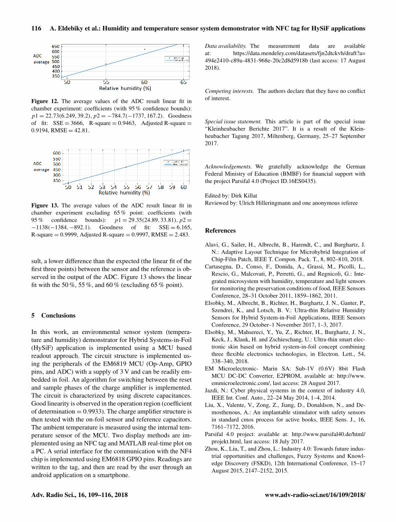
Next these obtained average values are used to check thelinearity of the performance of the complete system and toget a linear model (f (x)= p1 ·x+p2) to fit these values. Asan indication of the goodness of the linear fit, RMSE, SSE,R-square, and Adjusted R-square are calculated. As Fig. 12shows the results, quite good linearity is observed. However,the first calculated points at 50 %, 55 %, and 60 % humiditylevels respectively show a very linear behavior. On the otherside, the 65 % point is below this observed line. This can beexplained by taking into consideration that at higher relativehumidity the reference capacitor begins to increase. As a re-
www.adv-radio-sci.net/16/109/2018/ Adv. Radio Sci., 16, 109–116, 2018
116 A. Eldebiky et al.: Humidity and temperature sensor system demonstrator with NFC tag for HySiF applications
Figure 12. The average values of the ADC result linear fit inchamber experiment: coefficients (with 95 % confidence bounds):p1= 22.73(6.249,39.2),p2=−784.7(−1737,167.2). Goodnessof fit: SSE= 3666, R-square= 0.9463, Adjusted R-square=0.9194, RMSE= 42.81.
Figure 13. The average values of the ADC result linear fit inchamber experiment excluding 65 % point: coefficients (with95 % confidence bounds): p1= 29.35(24.89,33.81),p2=−1138(−1384,−892.1). Goodness of fit: SSE= 6.165,R-square= 0.9999, Adjusted R-square= 0.9997, RMSE= 2.483.
sult, a lower difference than the expected (the linear fit of thefirst three points) between the sensor and the reference is ob-served in the output of the ADC. Figure 13 shows the linearfit with the 50 %, 55 %, and 60 % (excluding 65 % point).
5 Conclusions
In this work, an environmental sensor system (tempera-ture and humidity) demonstrator for Hybrid Systems-in-Foil(HySiF) application is implemented using a MCU basedreadout approach. The circuit structure is implemented us-ing the peripherals of the EM6819 MCU (Op-Amp, GPIOpins, and ADC) with a supply of 3 V and can be readily em-bedded in foil. An algorithm for switching between the resetand sample phases of the charge amplifier is implemented.The circuit is characterized by using discrete capacitances.Good linearity is observed in the operation region (coefficientof determination= 0.9933). The charge amplifier structure isthen tested with the on-foil sensor and reference capacitors.The ambient temperature is measured using the internal tem-perature sensor of the MCU. Two display methods are im-plemented using an NFC tag and MATLAB real-time plot ona PC. A serial interface for the communication with the NF4chip is implemented using EM6818 GPIO pins. Readings arewritten to the tag, and then are read by the user through anandroid application on a smartphone.
Data availability. The measurement data are availableat: https://data.mendeley.com/datasets/fjn2dtckvh/draft?a=494e2410-c89a-4831-968e-20c2d8d5918b (last access: 17 August2018).
Competing interests. The authors declare that they have no conflictof interest.
Special issue statement. This article is part of the special issue“Kleinheubacher Berichte 2017”. It is a result of the Klein-heubacher Tagung 2017, Miltenberg, Germany, 25–27 September2017.
Acknowledgements. We gratefully acknowledge the GermanFederal Ministry of Education (BMBF) for financial support withthe project Parsifal 4.0 (Project ID.16ES0435).
Edited by: Dirk KillatReviewed by: Ulrich Hilleringmann and one anonymous referee
References
Alavi, G., Sailer, H., Albrecht, B., Harendt, C., and Burghartz, J.N.: Adaptive Layout Technique for Microhybrid Integration ofChip-Film Patch, IEEE T. Compon. Pack. T., 8, 802–810, 2018.
Cartasegna, D., Conso, F., Donida, A., Grassi, M., Picolli, L.,Rescio, G., Malcovati, P., Perretti, G., and Regnicoli, G.: Inte-grated microsystem with humidity, temperature and light sensorsfor monitoring the preservation conditions of food, IEEE SensorsConference, 28–31 October 2011, 1859–1862, 2011.
Elsobky, M., Albrecht, B., Richter, H., Burghartz, J. N., Ganter, P.,Szendrei, K., and Lotsch, B. V.: Ultra-thin Relative HumiditySensors for Hybrid System-in-Foil Applications, IEEE SensorsConference, 29 October–1 November 2017, 1–3, 2017.
Elsobky, M., Mahsereci, Y., Yu, Z., Richter, H., Burghartz, J. N.,Keck, J., Klauk, H. and Zschieschang, U.: Ultra-thin smart elec-tronic skin based on hybrid system-in-foil concept combiningthree flexible electronics technologies, in Electron. Lett., 54,338–340, 2018.
EM Microelectronic- Marin SA: Sub-1V (0.6V) 8bit FlashMCU DC-DC Converter, E2PROM, available at: http://www.emmicroelectronic.com/, last access: 28 August 2017.
Jazdi, N.: Cyber physical systems in the context of industry 4.0,IEEE Int. Conf. Auto., 22–24 May 2014, 1–4, 2014.
Liu, X., Valente, V., Zong, Z., Jiang, D., Donaldson, N., and De-mosthenous, A.: An implantable stimulator with safety sensorsin standard cmos process for active books, IEEE Sens. J., 16,7161–7172, 2016.
Parsifal 4.0 project: available at: http://www.parsifal40.de/html/projekt.html, last access: 18 July 2017.
Zhou, K., Liu, T., and Zhou, L.: Industry 4.0: Towards future indus-trial opportunities and challenges, Fuzzy Systems and Knowl-edge Discovery (FSKD), 12th International Conference, 15–17August 2015, 2147–2152, 2015.
Adv. Radio Sci., 16, 109–116, 2018 www.adv-radio-sci.net/16/109/2018/