Embed Size (px)
Citation preview
HT46R064/065/066/0662/067
Enhanced A/D Type 8-Bit OTP MCU
Rev. 1.10 1 June 9, 2009
General Description
The Enhanced A/D MCUs are a series of 8-bit high per-
formance, RISC architecture microcontrollers specifi-
cally designed for a wide range of applications. The
usual Holtek microcontroller features of low power con-
sumption, I/O flexibility, timer functions, oscillator op-
tions, power down and wake-up functions, watchdog
timer and low voltage reset, combine to provide devices
with a huge range of functional options while still main-
taining a high level of cost effectiveness. The fully inte-
grated system oscillator HIRC, which requires no
external components and which has three frequency
selections, opens up a huge range of new application
possibilities for these devices, some of which may in-
clude industrial control, consumer products, household
appliances subsystem controllers, etc.
Features
CPU Features
� Operating voltage:
fSYS= 4MHz: 2.2V~5.5V
fSYS= 8MHz: 3.0V~5.5V
fSYS= 12MHz: 4.5V~5.5V
� Up to 0.33�s instruction cycle with 12MHz system
clock at VDD= 5V
� Idle/Sleep mode and wake-up functions to reduce
power consumption
� Oscillator types:
External high freuency Crystal -- HXT
External RC -- ERC
Internal RC -- HIRC
External low frequency crystal -- LXT
� Four operational modes: Normal, Slow, Idle, Sleep
� Fully integrated internal 4MHz, 8MHz and 12MHz
oscillator requires no external components
� Watchdog Timer function
� LIRC oscillator function for watchdog timer
� All instructions executed in one or two instruction
cycles
� Table read instructions
� 63 powerful instructions
� Up to 8-level subroutine nesting
� Bit manipulation instruction
� Low voltage reset function
� Wide range of available package types
Peripheral Features
� Up to 42 bidirectional I/O lines
� Up to 8 channel 12-bit ADC
� Up to 3 channel 8-bit PWM
� Software controlled 4-SCOM lines LCD driver with
1/2 bias
� External interrupt input shared with an I/O line
� Up to three 8-bit programmable Timer/Event
Counter with overflow interrupt and prescaler
� Time-Base function
� Programmable Frequency Divider - PFD
Technical Document
� Application Note� HA0075E MCU Reset and Oscillator Circuits Application Note

Selection Table
Part No.Program
Memory
Data
MemoryI/O
8-bit
Timer
Time
Base
HIRC
(MHz)
RTC
(LXT)
LCD
SCOMA/D PWM PFD Stack Package
HT46R064 1K�14 64�8 18 1 1 4/8/12 � � 12-bit�4 8-bit�1 � 416DIP/NSOP,
20DIP/SOP/SSOP
HT46R065 2K�15 96�8 22 2 1 4/8/12 � 4 12-bit�4 8-bit�1 � 6
16DIP/NSOP,
20DIP/SOP/SSOP,
24SKDIP/SOP/SSOP
HT46R066 4K�15 128�8 26 2 1 4/8/12 � 4 12-bit�8 8-bit�2 � 6
16DIP/NSOP,
20DIP/SOP/SSOP,
24/28SKDIP/SOP/SSOP
HT46R0662 4K�15 224�8 42 2 1 4/8/12 � (*) 4 12-bit�8 8-bit�2 � 624/28SKDIP/SOP/SSOP,
44QFP
HT46R067 8K�16 384�8 42 3 1 4/8/12 � (*) 4 12-bit�8 8-bit�3 � 824/28SKDIP/SOP/SSOP,
44QFP
Note: �*� the oscillator is connected to the XT1/XT2 pins with TinyPowerTM design.
Block Diagram
The following block diagram illustrates the main functional blocks.
HT46R064/065/066/0662/067
Rev. 1.10 2 June 9, 2009
� � � � �� � � � � �
� � � � �
� � �� � � �
� � � �� � � �
� � � �
� � �� � � � � �
� � �� � � � � �
� � � � � � � �� � � � �
� � � � !" � � � � � � �
� � � � � � � � �

Pin Assignment
HT46R064/065/066/0662/067
Rev. 1.10 3 June 9, 2009
� � # � � � � $
� � % � � &
� � ' � � (
� � ) � � *
+ � �
� � %
� � #
� � ,
� � � � � � � �� � � � � � � � � � �
( '
( %
( #
( ,
( &
( (
( $
� � -
(
&
,
#
%
'
)
�
� � � � � � � �� � � � � � � � � � � � � � � �
� � , � � . � � � . ,
� � & � � $ � � . &
� � ( � � � � � � . (
� � $ � � . $
+
� $
� (
� � $
� � (
� � &
� � # � � � � $
� � % � � &
� � ' � � (
� � ) � � *
+ � �
� ,
� &
� � %
� � #
� � ,
� � , � � . � � � . ,
� � & � � $ � � . &
� � ( � � � � � � . (
� � $ � � . $
+
� � $
� � (
� � &
& $
( -
( �
( )
( '
( %
( #
( ,
( &
( (
(
&
,
#
%
'
)
�
-
( $
� � � � � � � �� � � � � � � � � � �
� � # � � � � $ � � (
� � % � � &
� � ' � � (
� � ) � � *
+ � �
� � %
� � #
� � , � � � ,
( '
( %
( #
( ,
( &
( (
( $
� � -
(
&
,
#
%
'
)
�
� � , � � . � � � . ,
� � & � � $ � � . &
� � ( � � � � � � . (
� � $ � � . $
+
� � $ � � � $
� � ( � � � (
� � & � � � � &
� � � � � � � �� � � � � � � � � � � � � � � �
� � � � � � � �� � � � � � � � � � � � � � � � � �
& #
& ,
& &
& (
& $
( -
( �
( )
( '
( %
( #
( ,
(
&
,
#
%
'
)
�
-
( $
( (
( &
& $
( -
( �
( )
( '
( %
( #
( ,
( &
( (
(
&
,
#
%
'
)
�
-
( $
� � , � � . � � � . ,
� � & � � $ � � . &
� � ( � � � � � � . (
� � $ � � . $
+
� $
� (
� � $ � � � $
� � ( � � � (
� � & � � � � &
� � # � � � � $ � � (
� � % � � &
� � ' � � (
� � ) � � *
+ � �
� ,
� &
� � %
� � #
� � , � � � ,
� � , � � . � � � . ,
� � & � � $ � � . &
� � ( � � � � � � . (
� � $ � � . $
+
� '
� )
� $
� (
� � $ � � � $
� � ( � � � (
� � & � � � � &
� � # � � � � $ � � (
� � % � � &
� � ' � � (
� � ) � � *
+ � �
� %
� #
� ,
� &
� � %
� � #
� � , � � � ,
� � � � � � � �� � � � � � � � � � � � � � � �
� � # � � � � $ � � (
� � % � � &
� � ' � � (
� � ) � � *
+ � �
� , � � � � (
� &
� � % � / � . � 0
� � # � / � $ 0
� � , � � � , � / � � � 0
& $
( -
( �
( )
( '
( %
( #
( ,
( &
( (
(
&
,
#
%
'
)
�
-
( $
� � , � � . � � � . ,
� � & � � $ � � . &
� � ( � � � � � � . (
� � $ � � . $
+
� $ � � . #
� ( � � . %
� � $ � � � $
� � ( � � � (
� � & � � � � &
� � � � � � � �� � � � � � � � � � � � � � � � � �
� � # � � � � $ � � (
� � % � � &
� � ' � � (
� � ) � � *
+ � �
� %
� #
� , � � � � (
� &
� � % � / � . � 0
� � # � / � $ 0
� � , � � � , � / � � � 0
& #
& ,
& &
& (
& $
( -
( �
( )
( '
( %
( #
( ,
(
&
,
#
%
'
)
�
-
( $
( (
( &
� � , � � . � � � . ,
� � & � � $ � � . &
� � ( � � � � � � . (
� � $ � � . $
+
� ' � � . '
� ) � � . )
� $ � � . #
� ( � � . %
� � $ � � � $
� � ( � � � (
� � & � � � � &
� � � � � � � �� � � � � � � � � � � � � � � � � �
& �
& )
& '
& %
& #
& ,
& &
& (
& $
( -
( �
( )
( '
( %
(
&
,
#
%
'
)
�
-
( $
( (
( &
( ,
( #
� � , � � . � � � . ,
� � & � � $ � � . &
� � ( � � � � � � . (
� � $ � � . $
+
� ' � � . '
� ) � � . )
� $ � � . #
� ( � � . %
� � $
� � (
� � $ � � � $
� � ( � � � (
� � & � � � � &
� � # � � � � $ � � (
� � % � � &
� � ' � � (
� � ) � � *
+ � �
� %
� #
� , � � � � (
� &
� � ,
� � &
� � % � / � . � 0
� � # � / � $ 0
� � , � � � , � / � � � 0
� � � � � � � �� � � � � � � � � � �
� � # � � � � $ � � (
� � % � � &
� � ' � � (
� � ) � � *
+ � �
� , � � � � (
� � #
� � , � � � ,
( '
( %
( #
( ,
( &
( (
( $
� � -
(
&
,
#
%
'
)
�
� � , � � . � � � . ,
� � & � � $ � � . &
� � ( � � � � � � . (
� � $ � � . $
+
� � $ � � � $
� � ( � � � (
� � & � � � � &

Note: Bracketed pin names indicate non-default pinout remapping locations.
HT46R064/065/066/0662/067
Rev. 1.10 4 June 9, 2009
� � � � � � � � �� � � � � � � � � � � � � � � � � �
� � , � � . � � � . ,
� � & � � $ � � . &
� � ( � � � � � � . (
� � $ � � . $
+
� ' � � . '
� ) � � . )
� $ � � . #
� ( � � . %
� � $ � � � $
� � ( � � � (
� � & � � � � &
� � # � � � � $ � � (
� � % � � &
� � ' � � (
� � ) � � *
+ � �
� % � 1 � (
� # � 1 � &
� , � � � � (
� &
� � % � / � . � 0
� � # � / � $ 0
� � , � � � , � / � � � 0
& #
& ,
& &
& (
& $
( -
( �
( )
( '
( %
( #
( ,
(
&
,
#
%
'
)
�
-
( $
( (
( &
� � � � � � � � �� � � � � � � � � � � � � � � � � �
� � , � � . � � � . ,
� � & � � $ � � . &
� � ( � � � � � � . (
� � $ � � . $
+
� ' � � . '
� ) � � . )
� $ � � . #
� ( � � . %
� � $
� � (
� � $ � � � $
� � ( � � � (
� � & � � � � &
� � # � � � � $ � � (
� � % � � &
� � ' � � (
� � ) � � *
+ � �
� % � 1 � (
� # � 1 � &
� , � � � � (
� &
� � ,
� � &
� � % � / � . � 0
� � # � / � $ 0
� � , � � � , � / � � � 0
& �
& )
& '
& %
& #
& ,
& &
& (
& $
( -
( �
( )
( '
( %
(
&
,
#
%
'
)
�
-
( $
( (
( &
( ,
( #
+��
��)��
*
��'��
(
��%��
&
��#����$��(
��,��.
���.,
��&��$��.&
��(������.(
��$��.$
+
�'��.'
� % � 1 � (
� # � 1 � &
� , � � � � (� &
� � )
� � '
� � %
� � #� � ,
� � &
� � (
� � � � � � � � �� � � � � �
(
&
,
#
%
'
)
�
-
( $
( (( & ( , ( # ( % ( ' ( ) ( � ( - & $ & ( & &
& ,
& #
& %
& '
& )
& �
& -
, $
, (
, &
, ,, #, %, ', ), �, -# $# (# &# ,# #
��$
��)
��'
��%�/�.
�0
��#�/�
$0
��,���,�/�
��0
��&���&
��(���(
��$���$
��(
��$
� ) � � . )
� $ � � . #� ( � � . %
� * $
� * (
� * &
� * ,� * #
� * %
� * '
� * )
� % � 1 � (
� # � 1 � &� , � � � � (
� & � � � � &
� � )
� � '
� � %� � #
� � ,
� � & � � &
� � (
� � � � � � � �� � � � � �
(
&
,
#
%
'
)
�
-
( $
( (( & ( , ( # ( % ( ' ( ) ( � ( - & $ & ( & &
& ,
& #
& %
& '
& )
& �
& -
, $
, (
, &
, ,, #, %, ', ), �, -# $# (# &# ,# #
+��
��)��
*
��'��
(
��%��
&
��#����$��(
��,��.
���.,
��&��$��.&
��(������.(
��$��.$
+
�'��.'
� ) � � . )
� $ � � . #� ( � � . %
� * $
� * (
� * &
� * ,� * #
� * %
� * '
� * )
��$
��)
��'
��%�/�.
�0
��#�/�
$0
��,���,�/�
��0
��&���&
��(���(
��$���$
��(
��$
� � � � � � � �� � � � � � � � � � � � � � � � � �
� � , � � . � � � . ,
� � & � � $ � � . &
� � ( � � � � � � . (
� � $ � � . $
+
� ' � � . '
� ) � � . )
� $ � � . #
� ( � � . %
� � $ � � � $
� � ( � � � (
� � & � � � � &
� � # � � � � $ � � (
� � % � � &
� � ' � � (
� � ) � � *
+ � �
� % � 1 � (
� # � 1 � &
� , � � � � (
� & � � � � &
� � % � / � . � 0
� � # � / � $ 0
� � , � � � , � / � � � 0
& #
& ,
& &
& (
& $
( -
( �
( )
( '
( %
( #
( ,
(
&
,
#
%
'
)
�
-
( $
( (
( &
� � � � � � � �� � � � � � � � � � � � � � � � � �
� � , � � . � � � . ,
� � & � � $ � � . &
� � ( � � � � � � . (
� � $ � � . $
+
� ' � � . '
� ) � � . )
� $ � � . #
� ( � � . %
� � $
� � (
� � $ � � � $
� � ( � � � (
� � & � � � � &
� � # � � � � $ � � (
� � % � � &
� � ' � � (
� � ) � � *
+ � �
� % � 1 � (
� # � 1 � &
� , � � � � (
� & � � � � &
� � ,
� � & � � &
� � % � / � . � 0
� � # � / � $ 0
� � , � � � , � / � � � 0
& �
& )
& '
& %
& #
& ,
& &
& (
& $
( -
( �
( )
( '
( %
(
&
,
#
%
'
)
�
-
( $
( (
( &
( ,
( #

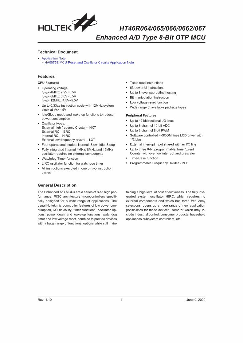
Pin Description
HT46R064
Pin Name Function OPT I/T O/T Description
PA0/AN0PA0
PAPU
PAWKST CMOS General purpose I/O. Register enabled pull-up and wake-up.
AN0 ADCR AN � A/D channel 0
PA1/PFD/AN1
PA1PAPU
PAWKST CMOS General purpose I/O. Register enabled pull-up and wake-up.
PFD CTRL0 � CMOS PFD output
AN1 ADCR AN � A/D channel 1
PA2/TC0/AN2
PA2PAPU
PAWKST CMOS General purpose I/O. Register enabled pull-up and wake-up.
TC0 � ST � External Timer 0 clock input
AN2 ADCR AN � A/D channel 2
PA3/INT/AN3
PA3PAPU
PAWKST CMOS General purpose I/O. Register enabled pull-up and wake-up.
INT � ST � External interrupt input
AN3 ADCR AN � A/D channel 3
PA4/PWM0PA4
PAPU
PAWKST CMOS General purpose I/O. Register enabled pull-up and wake-up.
PWM0 CTRL0 � CMOS PWM output
PA5/OSC2PA5
PAPU
PAWKST CMOS General purpose I/O. Register enabled pull-up and wake-up.
OSC2 CO � OSC Oscillator pin
PA6/OSC1PA6
PAPU
PAWKST CMOS General purpose I/O. Register enabled pull-up and wake-up.
OSC1 CO OSC � Oscillator pin
PA7/RESPA7 PAWK ST NMOS General purpose I/O. Register enabled wake-up.
RES CO ST � Reset input
PB0~PB5 PBn PBPU ST CMOS General purpose I/O. Register enabled pull-up.
PC0~PC3 PCn PCPU ST CMOS General purpose I/O. Register enabled pull-up.
VDD VDD � PWR � Power supply
VSS VSS � PWR � Ground
Note: I/T: Input type; O/T: Output type
OPT: Optional by configuration option (CO) or register option
PWR: Power; CO: Configuration option
ST: Schmitt Trigger input; CMOS: CMOS output; AN: analog input
SCOM= software controlled LCD COM
HXT: High frequency crystal oscillator
LXT: Low frequency crystal oscillator
HT46R064/065/066/0662/067
Rev. 1.10 5 June 9, 2009

HT46R065
Pin Name Function OPT I/T O/T Description
PA0/AN0PA0
PAPU
PAWKST CMOS General purpose I/O. Register enabled pull-up and wake-up.
AN0 ADCR AN � A/D channel 0
PA1/PFD/AN1
PA1PAPU
PAWKST CMOS General purpose I/O. Register enabled pull-up and wake-up.
PFD CTRL0 � CMOS PFD output
AN1 ADCR AN � A/D channel 1
PA2/TC0/AN2
PA2PAPU
PAWKST CMOS General purpose I/O. Register enabled pull-up and wake-up.
TC0 � ST � External Timer 0 clock input
AN2 ADCR AN � A/D channel 2
PA3/INT/AN3
PA3PAPU
PAWKST CMOS General purpose I/O. Register enabled pull-up and wake-up.
INT � ST � External interrupt input
AN3 ADCR AN � A/D channel 3
PA4/TC1/PWM0
PA4PAPU
PAWKST CMOS General purpose I/O. Register enabled pull-up and wake-up.
TC1 � ST � External Timer 1 clock input
PWM0 CTRL0 � CMOS PWM output
PA5/OSC2PA5
PAPU
PAWKST CMOS General purpose I/O. Register enabled pull-up and wake-up.
OSC2 CO � OSC Oscillator pin
PA6/OSC1PA6
PAPU
PAWKST CMOS General purpose I/O. Register enabled pull-up and wake-up.
OSC1 CO OSC � Oscillator pin
PA7/RESPA7 PAWK ST NMOS General purpose I/O. Register enabled wake-up.
RES CO ST � Reset input
PB0/SCOM0PB0 PBPU ST CMOS General purpose I/O. Register enabled pull-up.
SCOM0 SCOMC � SCOM Software controlled 1/2 bias LCD COM
PB1/SCOM1PB1 PBPU ST CMOS General purpose I/O. Register enabled pull-up.
SCOM1 SCOMC � SCOM Software controlled 1/2 bias LCD COM
PB2/SCOM2PB2 PBPU ST CMOS General purpose I/O. Register enabled pull-up.
SCOM2 SCOMC � SCOM Software controlled 1/2 bias LCD COM
PB3/SCOM3PB3 PBPU ST CMOS General purpose I/O. Register enabled pull-up.
SCOM3 SCOMC � SCOM Software controlled 1/2 bias LCD COM
PB4, PB5 PBn PBPU ST CMOS General purpose I/O. Register enabled pull-up.
PC0~PC7 PCn PCPU ST CMOS General purpose I/O. Register enabled pull-up.
VDD VDD � PWR � Power supply
VSS VSS � PWR � Ground
Note: I/T: Input type; O/T: Output type
OPT: Optional by configuration option (CO) or register option
PWR: Power; CO: Configuration option
ST: Schmitt Trigger input; CMOS: CMOS output; AN: analog input
SCOM: Software controlled LCD COM
HXT: High frequency crystal oscillator
LXT: Low frequency crystal oscillator
HT46R064/065/066/0662/067
Rev. 1.10 6 June 9, 2009

HT46R066
Pin Name Function OPT I/T O/T Description
PA0/AN0PA0
PAPU
PAWKST CMOS General purpose I/O. Register enabled pull-up and wake-up.
AN0 ADCR AN � A/D channel 0
PA1/PFD/AN1
PA1PAPU
PAWKST CMOS General purpose I/O. Register enabled pull-up and wake-up.
PFD CTRL0 � CMOS PFD output
AN1 ADCR AN � A/D channel 1
PA2/TC0/AN2
PA2PAPU
PAWKST CMOS General purpose I/O. Register enabled pull-up and wake-up.
TC0 � ST � External Timer 0 clock input
AN2 ADCR AN � A/D channel 2
PA3/INT/AN3
PA3PAPU
PAWKST CMOS General purpose I/O. Register enabled pull-up and wake-up.
INT � ST � External interrupt input
AN3 ADCR AN � A/D channel 3
PA4/TC1/PWM0
PA4PAPU
PAWKST CMOS General purpose I/O. Register enabled pull-up and wake-up.
TC1 � ST � External Timer 1 clock input
PWM0 CTRL0 � CMOS PWM output
PA5/OSC2PA5
PAPU
PAWKST CMOS General purpose I/O. Register enabled pull-up and wake-up.
OSC2 CO � OSC Oscillator pin
PA6/OSC1PA6
PAPU
PAWKST CMOS General purpose I/O. Register enabled pull-up and wake-up.
OSC1 CO OSC � Oscillator pin
PA7/RESPA7 PAWK ST NMOS General purpose I/O. Register enabled wake-up.
RES CO ST � Reset input
PB0/SCOM0PB0 PBPU ST CMOS General purpose I/O. Register enabled pull-up.
SCOM0 SCOMC � SCOM Software controlled 1/2 bias LCD COM
PB1/SCOM1PB1 PBPU ST CMOS General purpose I/O. Register enabled pull-up.
SCOM1 SCOMC � SCOM Software controlled 1/2 bias LCD COM
PB2/SCOM2PB2 PBPU ST CMOS General purpose I/O. Register enabled pull-up.
SCOM2 SCOMC � SCOM Software controlled 1/2 bias LCD COM
PB3/[PFD]/SCOM3
PB3 PBPU ST CMOS General purpose I/O. Register enabled pull-up.
PFD CTRL0 � CMOS PFD output
SCOM3 SCOMC � SCOM Software controlled 1/2 bias LCD COM
PB4/[TC0]PBn PBPU ST CMOS General purpose I/O. Register enabled pull-up.
TC0 CTRL0 ST � External Timer 0 clock input
PB5/[INT]PBn PBPU ST CMOS General purpose I/O. Register enabled pull-up.
INT CTRL0 ST � External interrupt input
HT46R064/065/066/0662/067
Rev. 1.10 7 June 9, 2009

Pin Name Function OPT I/T O/T Description
PC0/AN4
PC1/AN5
PC6/AN6
PC7/AN7
PCn PCPU ST CMOS General purpose I/O. Register enabled pull-up.
ANn ADCR AN � A/D channel 4, 5, 6, 7
PC2, PC4~PC5 PCn PCPU ST CMOS General purpose I/O. Register enabled pull-up.
PC3/PWM1PCn PCPU ST CMOS General purpose I/O. Register enabled pull-up.
PWM1 CTRL0 � CMOS PWM output
PD0~PD3 PDn PDPU ST CMOS General purpose I/O. Register enabled pull-up.
VDD VDD � PWR � Power supply
VSS VSS � PWR � Ground
Note: I/T: Input type; O/T: Output type
OPT: Optional by configuration option (CO) or register option
PWR: Power; CO: Configuration option
ST: Schmitt Trigger input; CMOS: CMOS output; AN: analog input
SCOM: Software controlled LCD COM
HXT: High frequency crystal oscillator
LXT: Low frequency crystal oscillator
HT46R0662, HT46R067
Pin Name Function OPT I/T O/T Description
PA0/AN0PA0
PAPU
PAWKST CMOS General purpose I/O. Register enabled pull-up and wake-up.
AN0 ADCR AN � A/D channel 0
PA1/PFD/AN1
PA1PAPU
PAWKST CMOS General purpose I/O. Register enabled pull-up and wake-up.
PFD CTRL0 � CMOS PFD output
AN1 ADCR AN � A/D channel 1
PA2/TC0/AN2
PA2PAPU
PAWKST CMOS General purpose I/O. Register enabled pull-up and wake-up.
TC0 � ST � External Timer 0 clock input
AN2 ADCR AN � A/D channel 2
PA3/INT/AN3
PA3PAPU
PAWKST CMOS General purpose I/O. Register enabled pull-up and wake-up.
INT � ST � External interrupt input
AN3 ADCR AN � A/D channel 3
PA4/TC1/PWM0
PA4PAPU
PAWKST CMOS General purpose I/O. Register enabled pull-up and wake-up.
TC1 � ST � External Timer 1 clock input
PWM0 CTRL0 � CMOS PWM output
PA5/OSC2PA5
PAPU
PAWKST CMOS General purpose I/O. Register enabled pull-up and wake-up.
OSC2 CO � OSC Oscillator pin
PA6/OSC1PA6
PAPU
PAWKST CMOS General purpose I/O. Register enabled pull-up and wake-up.
OSC1 CO OSC � Oscillator pin
HT46R064/065/066/0662/067
Rev. 1.10 8 June 9, 2009
Pin Name Function OPT I/T O/T Description
PA7/RESPA7 PAWK ST NMOS General purpose I/O. Register enabled wake-up.
RES CO ST � Reset input
PB0/SCOM0PB0 PBPU ST CMOS General purpose I/O. Register enabled pull-up.
SCOM0 SCOMC � SCOM Software controlled 1/2 bias LCD COM
PB1/SCOM1PB1 PBPU ST CMOS General purpose I/O. Register enabled pull-up.
SCOM1 SCOMC � SCOM Software controlled 1/2 bias LCD COM
PB2/SCOM2PB2 PBPU ST CMOS General purpose I/O. Register enabled pull-up.
SCOM2 SCOMC � SCOM Software controlled 1/2 bias LCD COM
PB3/[PFD]/SCOM3
PB3 PBPU ST CMOS General purpose I/O. Register enabled pull-up.
PFD CTRL0 � CMOS PFD output
SCOM3 SCOMC � SCOM Software controlled 1/2 bias LCD COM
PB4/[TC0]PBn PBPU ST CMOS General purpose I/O. Register enabled pull-up.
TC0 CTRL0 ST � External Timer 0 clock input
PB5/[INT]PBn PBPU ST CMOS General purpose I/O. Register enabled pull-up.
INT CTRL0 ST � External interrupt input
PB6~PB7 PBn PBPU ST CMOS General purpose I/O. Register enabled pull-up.
PC0/AN4
PC1/AN5
PC6/AN6
PC7/AN7
PCn PCPU ST CMOS General purpose I/O. Register enabled pull-up.
ANn ADCR AN � A/D channel 4, 5, 6, 7
PC2/PWM2PCn PCPU ST CMOS General purpose I/O. Register enabled pull-up.
PWM2 CTRL2 � CMOS PWM output - HT46R0662 doesnt have PWM2
PC3/PWM1PCn PCPU ST CMOS General purpose I/O. Register enabled pull-up.
PWM1 CTRL1 � CMOS PWM output
PC4/XT2PCn PCPU ST CMOS General purpose I/O. Register enabled pull-up.
XT2 CO � LXT Low frequency crystal pin
PC5/XT1PCn PCPU ST CMOS General purpose I/O. Register enabled pull-up.
XT1 CO � LXT Low frequency crystal pin
PD0, PD1
PD3~PD7PDn PDPU ST CMOS General purpose I/O. Register enabled pull-up.
PD2/TC2PDn PDPU ST CMOS General purpose I/O. Register enabled pull-up.
TC2 � ST � External Timer 2 clock input - HT46R0662 doesnt have TC2
PE0~PE7 PEn PEPU ST CMOS General purpose I/O. Register enabled pull-up.
PF0, PF1 PFn PFPU ST CMOS General purpose I/O. Register enabled pull-up.
VDD VDD � PWR � Power supply
VSS VSS � PWR � Ground
Note: I/T: Input type; O/T: Output type
OPT: Optional by configuration option (CO) or register option
PWR: Power; CO: Configuration option
ST: Schmitt Trigger input; CMOS: CMOS output; AN: analog input
SCOM: Software controlled LCD COM
HXT: High frequency crystal oscillator
LXT: Low frequency crystal oscillator
HT46R064/065/066/0662/067
Rev. 1.10 9 June 9, 2009

Absolute Maximum Ratings
Supply Voltage ...........................VSS�0.3V to VSS+6.0V Storage Temperature ............................�50C to 125C
Input Voltage..............................VSS�0.3V to VDD+0.3V Operating Temperature...........................�40C to 85CIOL Total ..............................................................100mA IOH Total............................................................�100mA
Total Power Dissipation .....................................500mW
Note: These are stress ratings only. Stresses exceeding the range specified under �Absolute Maximum Ratings� may
cause substantial damage to the device. Functional operation of this device at other conditions beyond those listed
in the specification is not implied and prolonged exposure to extreme conditions may affect device reliability.
D.C. Characteristics Ta=25C
Symbol ParameterTest Conditions
Min. Typ. Max. UnitVDD Conditions
VDD Operating Voltage �
fSYS=4MHz 2.2 � 5.5 V
fSYS=8MHz 3.0 � 5.5 V
fSYS=12MHz 4.5 � 5.5 V
IDD1Operating Current
(HXT, HIRC, ERC)
3VNo load, fSYS=4MHz
� 0.8 1.2 mA
5V � 1.5 2.25 mA
IDD2Operating Current
(HXT, HIRC, ERC)
3VNo load, fSYS=8MHz
� 1.4 2.1 mA
5V � 2.8 4.2 mA
IDD3Operating Current
(HXT, HIRC, ERC)5V No load, fSYS=12MHz � 4 6 mA
IDD4Operating Current
(HIRC + LXT, Slow Mode)
3V No load, fSYS=32768Hz
(LXT on OSC1/OSC2,
LVR disabled, LXTLP=1)
� 5 10 �A
5V � 12 24 �A
3V No load, fSYS=32768Hz
(LXT on XT1/XT2,
LVR disabled, LXTLP=1)
� 5 10 �A
5V � 10 20 �A
ISTB1Standby Current
(LIRC On, LXT Off)
3VNo load, system HALT
� � 5 �A
5V � � 10 �A
ISTB2Standby Current
(LIRC Off, LXT Off)
3VNo load, system HALT
� � 1 �A
5V � � 2 �A
ISTB3Standby Current
(LIRC Off, LXT On, LXTLP=1)
3V No load, system HALT
(LXT on OSC1/OSC2)
� � 5 �A
5V � � 10 �A
3V No load, system HALT
(LXT on XT1/XT2)
� � 3 �A
5V � � 5 �A
VIL1Input Low Voltage for I/O,
TCn and INT� � 0 � 0.3VDD V
VIH1Input High Voltage for I/O,
TCn and INT� � 0.7VDD � VDD V
VIL2 Input Low Voltage (RES) � � 0 � 0.4VDD V
VIH2 Input High Voltage (RES) � � 0.9VDD � VDD V
VLVR1 Low Voltage Reset 1 � VLVR = 4.2V 3.98 4.2 4.42 V
VLVR2 Low Voltage Reset 2 � VLVR = 3.15V 2.98 3.15 3.32 V
VLVR3 Low Voltage Reset 3 � VLVR = 2.1V 1.98 2.1 2.22 V
HT46R064/065/066/0662/067
Rev. 1.10 10 June 9, 2009

Symbol ParameterTest Conditions
Min. Typ. Max. UnitVDD Conditions
IOL1I/O Port Sink Current
(PA, PB, PC)
3VVOL=0.1VDD
4 8 � mA
5V 10 20 � mA
IOH I/O Port Source Current3V
VOH=0.9VDD
�2 �4 � mA
5V �5 �10 � mA
IOL2 PA7 Sink Current 5V VOL=0.1VDD 2 3 � mA
RPH Pull-high Resistance3V � 20 60 100 k�
5V � 10 30 50 k�
ISCOM SCOM Operating Current 5V
SCOMC, ISEL[1:0]=00 17.5 25.0 32.5 �A
SCOMC, ISEL[1:0]=01 35 50 65 �A
SCOMC, ISEL[1:0]=10 70 100 130 �A
SCOMC, ISEL[1:0]=11 140 200 260 �A
VSCOM VDD/2 Voltage for LCD COM 5V No load 0.475 0.500 0.525 VDD
Note: The standby current (ISTB1~ISTB3) and IDD4 are measured with all I/O pins in input mode and tied to VDD.
A.C. Characteristics Ta=25C
Symbol ParameterTest Conditions
Min. Typ. Max. UnitVDD Conditions
fSYS System Clock �
2.2V~5.5V 32 � 4000 kHz
3.0V~5.5V 32 � 8000 kHz
4.5V~5.5V 32 � 12000 kHz
fHIRCSystem Clock
(HIRC)
3V/5V Ta=25C �2% 4 +2% MHz
3V/5V Ta=25C �2% 8 +2% MHz
5V Ta=25C �2% 12 +2% MHz
3V/5V Ta=0~70C �5% 4 +5% MHz
3V/5V Ta=0~70C �5% 8 +5% MHz
5V Ta=0~70C �5% 12 +5% MHz
2.2V~
3.6VTa=0~70C �8% 4 +8% MHz
3.0V~
5.5VTa=0~70C �8% 4 +8% MHz
3.0V~
5.5VTa=0~70C �8% 8 +8% MHz
4.5V~
5.5VTa=0~70C �8% 12 +8% MHz
2.2V~
3.6VTa= �40C~85C �12% 4 +12% MHz
3.0V~
5.5VTa= �40C~85C �12% 4 +12% MHz
3.0V~
5.5VTa= �40C~85C �12% 8 +12% MHz
4.5V~
5.5VTa= �40C~85C �12% 12 +12% MHz
HT46R064/065/066/0662/067
Rev. 1.10 11 June 9, 2009
Ta=25C

Symbol ParameterTest Conditions
Min. Typ. Max. UnitVDD Conditions
fERCSystem Clock
(ERC)
5V Ta=25C, R=120k� * �2% 4 +2% MHz
5V Ta=0~70C, R=120k� * �5% 4 +5% MHz
5VTa= �40C~85C,
R=120k� *�7% 4 +7% MHz
2.2V~
5.5V
Ta= �40C~85C,
R=120k� *�11% 4 +11% MHz
fLXT System Clock (LXT) � � � 32768 � Hz
fTIMERTimer Input Frequency
(TCn)�
2.2V~5.5V 0 � 4000 kHz
3.0V~5.5V 0 � 8000 kHz
4.5V~5.5V 0 � 12000 kHz
fLIRC LIRC Oscillator3V � 5 10 15 kHz
5V � 6.5 13 19.5 kHz
tRES External Reset Low Pulse Width � � 1 � � �s
tSST System Start-up time Period �
For HXT/LXT � 1024 � tSYS
For ERC/IRC
(By configuration option)
� 2 � tSYS
� 1024 � tSYS
tINT Interrupt Pulse Width � � 1 � � �s
tLVR Low Voltage Width to Reset � � 0.25 1 2 ms
RESTD Reset Delay Time � � � 100 � ms
Note: 1. tSYS=1/fSYS
2. *For fERC, as the resistor tolerance will influence the frequency a precision resistor is recommended.
3. For the HT46R065 devices, the fERC parameter is not applicable.
4. To maintain the accuracy of the internal HIRC oscillator frequency, a 0.1�F decoupling capacitor should
be connected between VDD and VSS and located as close to the device as possible.
ADC Characteristics Ta=25C
Symbol ParameterTest Conditions
Min. Typ. Max. UnitVDD Conditions
DNL A/C Differential Non-Linearity3V
tAD=0.5�s �2 � 2 LSB5V
INL ADC Integral Non-Linearity3V
tAD=0.5�s �4 � 4 LSB5V
IADCAdditional Power Consumption
if A/D Converter is Used
3V�
� 0.5 0.75 mA
5V � 1.0 1.5 mA
HT46R064/065/066/0662/067
Rev. 1.10 12 June 9, 2009
Ta=25C
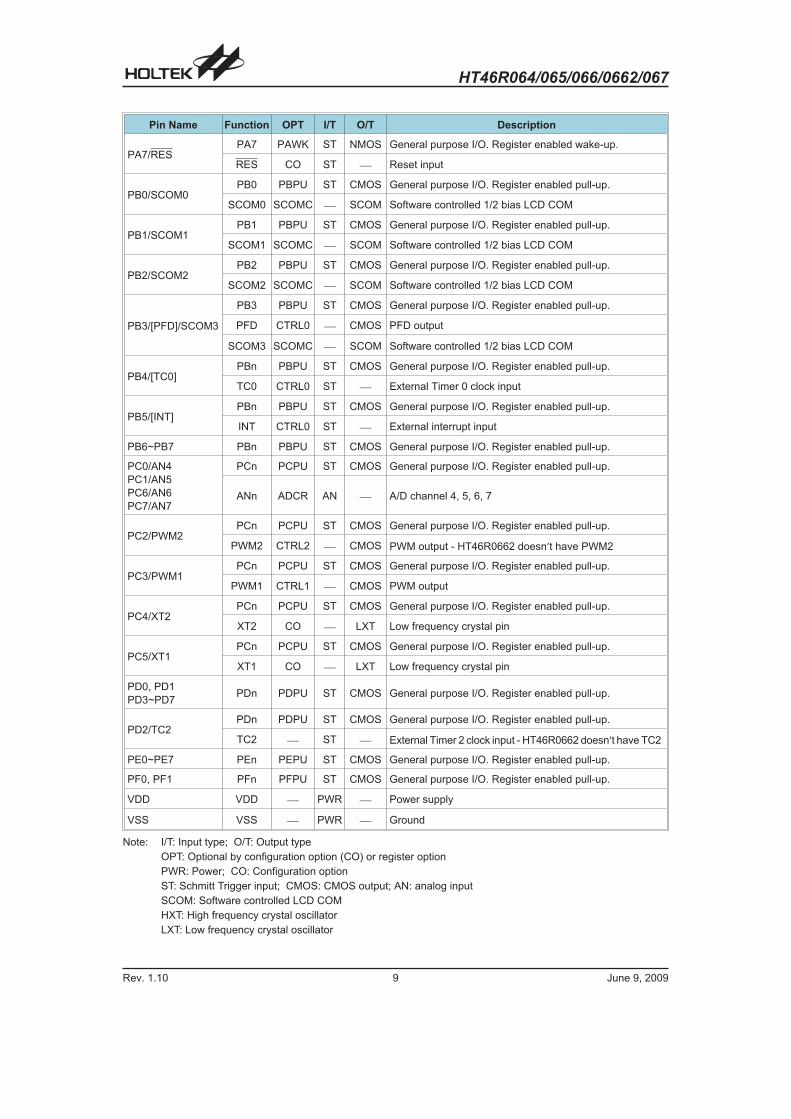
Power-on Reset Characteristics
Symbol ParameterTest Conditions
Min. Typ. Max. UnitVDD Conditions
VPORVDD Start Voltage to Ensure
Power-on Reset� � � � 100 mV
RRVDDVDD raising rate to Ensure
Power-on Reset� � 0.035 � � V/ms
tPORMinimum Time for VDD Stays at
VPOR to Ensure Power-on Reset� � 1 � � ms
HT46R064/065/066/0662/067
Rev. 1.10 13 June 9, 2009
� � � �
+ � �
+ � � �
� � + � �� � � �
HT46R064/065/066/0662/067
Rev. 1.10 14 June 9, 2009
System Architecture
A key factor in the high-performance features of the
Holtek range of microcontrollers is attributed to the inter-
nal system architecture. The range of devices take ad-
vantage of the usual features found within RISC
microcontrollers providing increased speed of operation
and enhanced performance. The pipelining scheme is
implemented in such a way that instruction fetching and
instruction execution are overlapped, hence instructions
are effectively executed in one cycle, with the exception
of branch or call instructions. An 8-bit wide ALU is used
in practically all operations of the instruction set. It car-
ries out arithmetic operations, logic operations, rotation,
increment, decrement, branch decisions, etc. The inter-
nal data path is simplified by moving data through the
Accumulator and the ALU. Certain internal registers are
implemented in the Data Memory and can be directly or
indirectly addressed. The simple addressing methods of
these registers along with additional architectural fea-
tures ensure that a minimum of external components is
required to provide a functional I/O and A/D control sys-
tem with maximum reliability and flexibility.
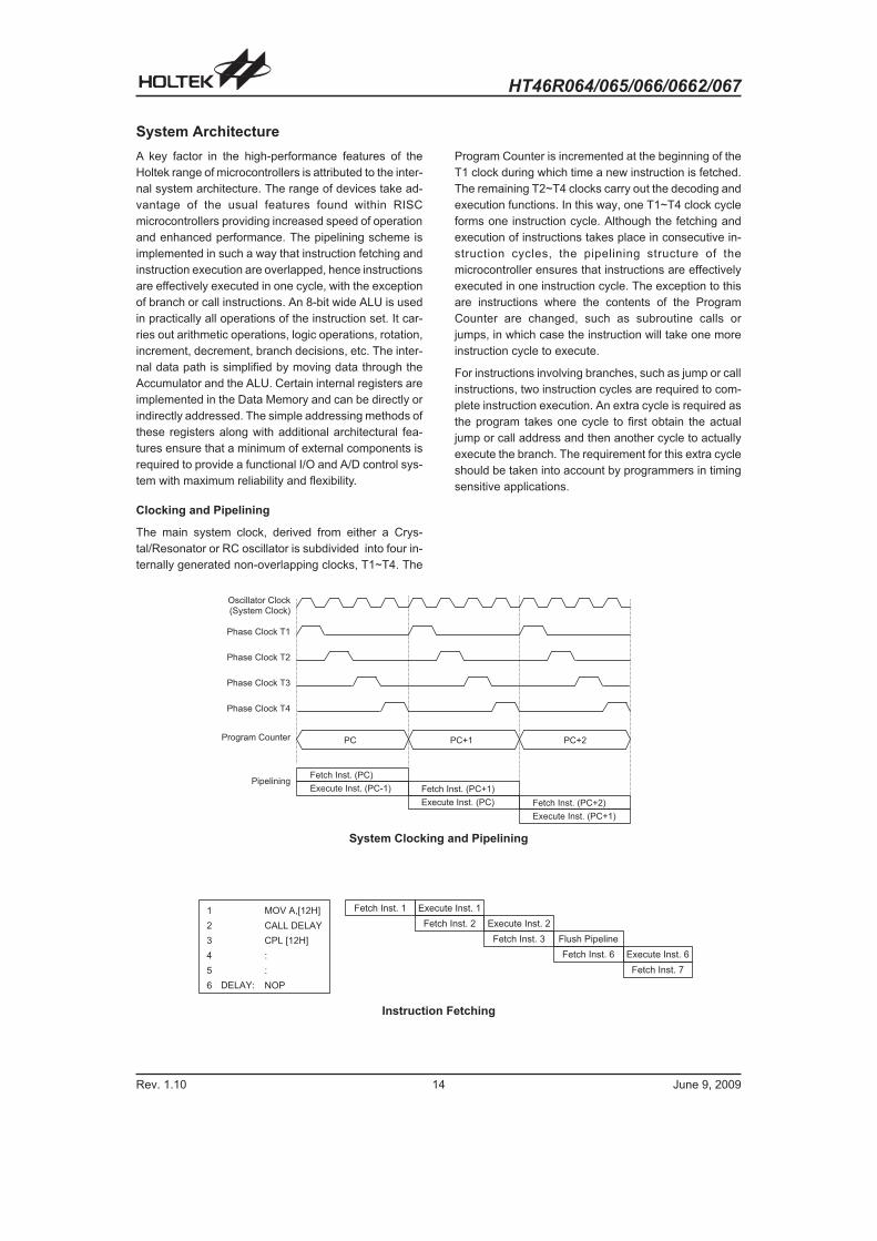
Clocking and Pipelining
The main system clock, derived from either a Crys-
tal/Resonator or RC oscillator is subdivided into four in-
ternally generated non-overlapping clocks, T1~T4. The
Program Counter is incremented at the beginning of the
T1 clock during which time a new instruction is fetched.
The remaining T2~T4 clocks carry out the decoding and
execution functions. In this way, one T1~T4 clock cycle
forms one instruction cycle. Although the fetching and
execution of instructions takes place in consecutive in-
struction cycles, the pipelining structure of the
microcontroller ensures that instructions are effectively
executed in one instruction cycle. The exception to this
are instructions where the contents of the Program
Counter are changed, such as subroutine calls or
jumps, in which case the instruction will take one more
instruction cycle to execute.
For instructions involving branches, such as jump or call
instructions, two instruction cycles are required to com-
plete instruction execution. An extra cycle is required as
the program takes one cycle to first obtain the actual
jump or call address and then another cycle to actually
execute the branch. The requirement for this extra cycle
should be taken into account by programmers in timing
sensitive applications.
� � � 2 3 � � � � 4 � 5 � 6
* 7 � 2 8 � � � � � � 4 � 5 � � ( 6 � � � 2 3 � � � � 4 � 5 � 9 ( 6
* 7 � 2 8 � � � � � � 4 � 5 � 6 � � � 2 3 � � � � 4 � 5 � 9 & 6
* 7 � 2 8 � � � � � � 4 � 5 � 9 ( 6
� � 9 ( � 9 &
� � 2 � : : � � � � : 2 ;5 � � � � � � : 2 ; 6
� 3 � � � � : 2 ; � � (
� � ! � � � � 8 � � �
� 3 � � � � : 2 ; � � &
� 3 � � � � : 2 ; � � ,
� 3 � � � � : 2 ; � � #
� � < � : � � !
System Clocking and Pipelining
� � � 2 3 � � � � 4 � ( * 7 � 2 8 � � � � � � 4 � (
� � � 2 3 � � � � 4 � &
� : 8 � 3 � � � < � : � �
(
&
,
#
%
' � * � � = >
� � + � � ? / ( & @ 0
� � � � � * � � =
� � � / ( & @ 0
>
>
. � �
* 7 � 2 8 � � � � � � 4 � &
� � � 2 3 � � � � 4 � ,
� � � 2 3 � � � � 4 � ' * 7 � 2 8 � � � � � � 4 � '
� � � 2 3 � � � � 4 � )
Instruction Fetching

HT46R064/065/066/0662/067
Rev. 1.10 15 June 9, 2009
Program Counter
During program execution, the Program Counter is used
to keep track of the address of the next instruction to be
executed. It is automatically incremented by one each
time an instruction is executed except for instructions,
such as �JMP� or �CALL� that demand a jump to a
non-consecutive Program Memory address. Note that
the Program Counter width varies with the Program
Memory capacity depending upon which device is se-
lected. However, it must be noted that only the lower 8
bits, known as the Program Counter Low Register, are
directly addressable by user.
When executing instructions requiring jumps to
non-consecutive addresses such as a jump instruction,
a subroutine call, interrupt or reset, etc., the
microcontroller manages program control by loading the
required address into the Program Counter. For condi-
tional skip instructions, once the condition has been
met, the next instruction, which has already been
fetched during the present instruction execution, is dis-
carded and a dummy cycle takes its place while the cor-
rect instruction is obtained.
Device
Program Counter
Program Counter
High BytePCL Register
HT46R064 PC9,PC8
PCL7~PCL0
HT46R065 PC10~PC8
HT46R066
HT46R0662PC11~PC8
HT46R067 PC12~PC8
The lower byte of the Program Counter, known as the
Program Counter Low register or PCL, is available for
program control and is a readable and writeable regis-
ter. By transferring data directly into this register, a short
program jump can be executed directly, however, as
only this low byte is available for manipulation, the
jumps are limited to the present page of memory, that is
256 locations. When such program jumps are executed
it should also be noted that a dummy cycle will be in-
serted.
The lower byte of the Program Counter is fully accessi-
ble under program control. Manipulating the PCL might
cause program branching, so an extra cycle is needed
to pre-fetch. Further information on the PCL register can
be found in the Special Function Register section.
Stack
This is a special part of the memory which is used to
save the contents of the Program Counter only. The
stack is neither part of the Data or Program Memory
space, and is neither readable nor writeable. The acti-
vated level is indexed by the Stack Pointer, SP, and is
neither readable nor writeable. At a subroutine call or in-
terrupt acknowledge signal, the contents of the Program
Counter are pushed onto the stack. At the end of a sub-
routine or an interrupt routine, signaled by a return in-
struction, RET or RETI, the Program Counter is restored
to its previous value from the stack. After a device reset,
the Stack Pointer will point to the top of the stack.
Device Stack Levels
HT46R064 4
HT46R065
HT46R066
HT46R0662
6
HT46R067 8
If the stack is full and an enabled interrupt takes place,
the interrupt request flag will be recorded but the ac-
knowledge signal will be inhibited. When the Stack
Pointer is decremented, by RET or RETI, the interrupt
will be serviced. This feature prevents stack overflow al-
lowing the programmer to use the structure more easily.
However, when the stack is full, a CALL subroutine in-
struction can still be executed which will result in a stack
overflow. Precautions should be taken to avoid such
cases which might cause unpredictable program
branching.
Arithmetic and Logic Unit � ALU
The arithmetic-logic unit or ALU is a critical area of the
microcontroller that carries out arithmetic and logic op-
erations of the instruction set. Connected to the main
microcontroller data bus, the ALU receives related in-
struction codes and performs the required arithmetic or
logical operations after which the result will be placed in
the specified register. As these ALU calculation or oper-
ations may result in carry, borrow or other status
changes, the status register will be correspondingly up-
dated to reflect these changes. The ALU supports the
following functions:
� Arithmetic operations: ADD, ADDM, ADC, ADCM,
SUB, SUBM, SBC, SBCM, DAA
� Logic operations: AND, OR, XOR, ANDM, ORM,
XORM, CPL, CPLA
� Rotation RRA, RR, RRCA, RRC, RLA, RL, RLCA,
RLC
� Increment and Decrement INCA, INC, DECA, DEC
� � ! � � � � 8 � � �
� � 2 ; � � � � � : � (
� � 2 ; � � � � � : � &
� � 2 ; � � � � � : � ,
� � 2 ; � � � � � : � �
� � ! � � �� � � � �
� < � A � � � 2 ;
� � 2 ;� � � � �
� � � � � A � � � 2 ;

HT46R064/065/066/0662/067
Rev. 1.10 16 June 9, 2009
� Branch decision, JMP, SZ, SZA, SNZ, SIZ, SDZ,
SIZA, SDZA, CALL, RET, RETI
Program Memory
The Program Memory is the location where the user
code or program is stored. The device is supplied with
One-Time Programmable, OTP, memory where users
can program their application code into the device. By
using the appropriate programming tools, OTP devices
offer users the flexibility to freely develop their applica-
tions which may be useful during debug or for products
requiring frequent upgrades or program changes.
Structure
The Program Memory has a capacity of 1K�14 to
8K�16. The Program Memory is addressed by the Pro-
gram Counter and also contains data, table information
and interrupt entries. Table data, which can be setup in
any location within the Program Memory, is addressed
by separate table pointer registers.
Device Capacity
HT46R064 1K�14
HT46R065 2K�15
HT46R066
HT46R06624K�15
HT46R067 8K�16
Special Vectors
Within the Program Memory, certain locations are re-
served for special usage such as reset and interrupts.
� Reset Vector
This vector is reserved for use by the device reset for
program initialisation. After a device reset is initiated, the
program will jump to this location and begin execution.
� External interrupt vector
This vector is used by the external interrupt. If the ex-
ternal interrupt pin on the device receives an edge
transition, the program will jump to this location and
begin execution if the external interrupt is enabled and
the stack is not full. The external interrupt active edge
transition type, whether high to low, low to high or both
is specified in the CTRL1 register.
� Timer/Event 0/1/2 counter interrupt vector
This internal vector is used by the Timer/Event Coun-
ters. If a Timer/Event Counter overflow occurs, the
program will jump to its respective location and begin
execution if the associated Timer/Event Counter inter-
rupt is enabled and the stack is not full.
� Time base interrupt vector
This internal vector is used by the internal Time Base.
If a Time Base overflow occurs, the program will jump
to this location and begin execution if the Time Base
counter interrupt is enabled and the stack is not full.
$ $ @
� � � � � � � � � � � � � � � �
� � � � �
� � � � � � � �� � � � � � � � � � � � � � � � �
) � � @
, � � @
* 7 � � � � :� � � � � 8 < �
� � � � � � $� � � � � 8 < �
� � � � � � � � �� � � � � 8 < �
� � � � �
* 7 � � � � :� � � � � 8 < �
� � � � � � $� � � � � 8 < �
� � � � � � � � �� � � � � 8 < �
� � � � �
* 7 � � � � :� � � � � 8 < �
� � � � � � $� � � � � 8 < �
� � � � � � � � �� � � � � 8 < �
� � � � �
* 7 � � � � :� � � � � 8 < �
� � � � � � $� � � � � 8 < �
� � � � � � (� � � � � 8 < �
� � � � � � � � �� � � � � 8 < �
� � � � � � (� � � � � 8 < �
� � � � � � &� � � � � 8 < �
$ # @
$ � @
$ @
( $ @
( # @
( � @
� � � @
( � � � @
( # � � � � �
( % � � � � �
( % � � � � �
( ' � � � � �
� � �� � � � � 8 < �
� � � � � � (� � � � � 8 < �
� � �� � � � � 8 < �
� � �� � � � � 8 < �
� � �� � � � � 8 < �
Program Memory Structure

HT46R064/065/066/0662/067
Rev. 1.10 17 June 9, 2009
Look-up Table
Any location within the Program Memory can be defined
as a look-up table where programmers can store fixed
data. To use the look-up table, the table pointer must
first be setup by placing the lower order address of the
look up data to be retrieved in the table pointer register,
TBLP. This register defines the lower 8-bit address of
the look-up table.
After setting up the table pointer, the table data can be
retrieved from the current Program Memory page or last
Program Memory page using the �TABRDC[m]� or
�TABRDL [m]� instructions, respectively. When these in-
structions are executed, the lower order table byte from
the Program Memory will be transferred to the user de-
fined Data Memory register [m] as specified in the in-
struction. The higher order table data byte from the
Program Memory will be transferred to the TBLH special
register. Any unused bits in this transferred higher order
byte will be read as �0�.
The following diagram illustrates the addressing/data
flow of the look-up table:
Table Program Example
The accompanying example shows how the table
pointer and table data is defined and retrieved from the
device. This example uses raw table data located in the
last page which is stored there using the ORG state-
ment. The value at this ORG statement is �300H� which
refers to the start address of the last page within the 1K
Program Memory of the HT46R064 microcontrollers.
The table pointer is setup here to have an initial value of
�06H�. This will ensure that the first data read from the
data table will be at the Program Memory address
�306H� or 6 locations after the start of the last page.
Note that the value for the table pointer is referenced to
the first address of the present page if the �TABRDC
[m]� instruction is being used. The high byte of the table
data which in this case is equal to zero will be trans-
ferred to the TBLH register automatically when the
�TABRDL [m]� instruction is executed.
Because the TBLH register is a read-only register and
cannot be restored, care should be taken to ensure its
protection if both the main routine and Interrupt Service
Routine use the table read instructions. If using the table
read instructions, the Interrupt Service Routines may
change the value of TBLH and subsequently cause er-
rors if used again by the main routine. As a rule it is rec-
ommended that simultaneous use of the table read
instructions should be avoided. However, in situations
where simultaneous use cannot be avoided, the inter-
rupts should be disabled prior to the execution of any
main routine table-read instructions. Note that all table
related instructions require two instruction cycles to
complete their operation.
� � ! � � � � � � � � � @� � � � � � : � 2 � � B
� � ! � � � � �
@ � ! 3 � � � � � � C � � � � �
� � � � � < � ! � � �< � � � � � � < � ! �� 7 D � �
� � @ � ! 3 � � � � �
� � � � � � � ! � � � � �
� � � �
�BB���� ( # D ( ' � � � � �
� � � � � � � � � � � !
InstructionTable Location Bits
b12 b11 b10 b9 b8 b7 b6 b5 b4 b3 b2 b1 b0
TABRDC [m] PC12 PC11 PC10 PC9 PC8 @7 @6 @5 @4 @3 @2 @1 @0
TABRDL [m] 1 1 1 1 1 @7 @6 @5 @4 @3 @2 @1 @0
Table Location
Note: PC12~PC8: Current Program Counter bits
@7~@0: Table Pointer TBLP bits
For the HT46R064, the Table address location is 10 bits, i.e. from b9~b0.
For the HT46R065, the Table address location is 11 bits, i.e. from b10~b0.
For the HT46R066/HT46R0662, the Table address location is 12 bits, i.e. from b11~b0
For the HT46R067, the Table address location is 13 bits, i.e. from b12~b0

HT46R064/065/066/0662/067
Rev. 1.10 18 June 9, 2009
Table Read Program Example:
tempreg1 db ? ; temporary register #1tempreg2 db ? ; temporary register #2
::
mov a,06h ; initialise table pointer - note that this address; is referenced
mov tblp,a ; to the last page or present page::
tabrdl tempreg1 ; transfers value in table referenced by table pointer; to tempregl; data at prog. memory address �306H� transferred to; tempreg1 and TBLH
dec tblp ; reduce value of table pointer by one
tabrdl tempreg2 ; transfers value in table referenced by table pointer; to tempreg2; data at prog.memory address �305H� transferred to; tempreg2 and TBLH; in this example the data �1AH� is transferred to; tempreg1 and data �0FH� to register tempreg2; the value �00H� will be transferred to the high byte; register TBLH
::
org 300h ; sets initial address of last page
dc 00Ah, 00Bh, 00Ch, 00Dh, 00Eh, 00Fh, 01Ah, 01Bh::
Data Memory
The Data Memory is a volatile area of 8-bit wide RAM
internal memory and is the location where temporary in-
formation is stored.
Structure
Divided into two sections, the first of these is an area of
RAM where special function registers are located. These
registers have fixed locations and are necessary for cor-
rect operation of the device. Many of these registers can
be read from and written to directly under program con-
trol, however, some remain protected from user manipu-
lation. The second area of Data Memory is reserved for
general purpose use. All locations within this area are
read and write accessible under program control.
Device Capacity Banks
HT46R064 64�8 �
HT46R065 96�8 �
HT46R066 128�8 �
HT46R0662 224�8 0, 1
HT46R067 384�8 0, 1
The two sections of Data Memory, the Special Purpose
and General Purpose Data Memory are located at con-
secutive locations. All are implemented in RAM and are 8
bits wide but the length of each memory section is dic-
tated by the type of microcontroller chosen. The start ad-
dress of the Data Memory for all devices is the address
�00H�.
All microcontroller programs require an area of
read/write memory where temporary data can be stored
and retrieved for use later. It is this area of RAM memory
that is known as General Purpose Data Memory. This
area of Data Memory is fully accessible by the user pro-
gram for both read and write operations. By using the
�SET [m].i� and �CLR [m].i� instructions individual bits
can be set or reset under program control giving the
user a large range of flexibility for bit manipulation in the
Data Memory.
For some devices, the Data Memory is subdivided into
two banks, which are selected using a Bank Pointer.
Only data in Bank 0 can be directly addressed, data in
Bank 1 must be indirectly addressed.

HT46R064/065/066/0662/067
Rev. 1.10 19 June 9, 2009
Special Purpose Data Memory
This area of Data Memory is where registers, necessary
for the correct operation of the microcontroller, are
stored. Most of the registers are both readable and
writeable but some are protected and are readable only,
the details of which are located under the relevant Spe-
cial Function Register section. Note that for locations
that are unused, any read instruction to these addresses
will return the value �00H�.
Special Function Registers
To ensure successful operation of the microcontroller,
certain internal registers are implemented in the Data
Memory area. These registers ensure correct operation
of internal functions such as timers, interrupts, etc., as
well as external functions such as I/O data control. The
location of these registers within the Data Memory be-
gins at the address �00H� and are mapped into both
Bank 0 and Bank 1. Any unused Data Memory locations
between these special function registers and the point
where the General Purpose Memory begins is reserved
and attempting to read data from these locations will re-
turn a value of �00H�.
Indirect Addressing Registers � IAR0, IAR1
The Indirect Addressing Registers, IAR0 and IAR1, al-
though having their locations in normal RAM register
space, do not actually physically exist as normal regis-
ters. The method of indirect addressing for RAM data
manipulation uses these Indirect Addressing Registers
and Memory Pointers, in contrast to direct memory ad-
dressing, where the actual memory address is speci-
fied. Actions on the IAR0 and IAR1 registers will result in
no actual read or write operation to these registers but
rather to the memory location specified by their corre-
sponding Memory Pointer, MP0 or MP1. Acting as a
pair, IAR0 with MP0 and IAR1 with MP1 can together ac-
cess data from the Data Memory. As the Indirect Ad-
dressing Registers are not physically implemented,
reading the Indirect Addressing Registers indirectly will
return a result of �00H� and writing to the registers indi-
rectly will result in no operation.
Memory Pointers � MP0, MP1
Two Memory Pointers, known as MP0 and MP1 are pro-
vided. These Memory Pointers are physically imple-
mented in the Data Memory and can be manipulated in
the same way as normal registers providing a conve-
nient way with which to indirectly address and track
data. MP0 can only be used to indirectly address data in
Bank 0 while MP1 can be used to address data in Bank
0 and Bank1. When any operation to the relevant Indi-
rect Addressing Registers is carried out, the actual ad-
dress that the microcontroller is directed to, is the
address specified by the related Memory Pointer. Note
that for the HT46R064 device, bit 7 of the Memory
Pointers is not required to address the full memory
space. When bit 7 of the Memory Pointers for these de-
vices is read, a value of �1� will be returned. Note that in-
direct addressing using MP1 and IAR1 must be used to
access any data in Bank 1. The following example shows
how to clear a section of four Data Memory locations al-
ready defined as locations adres1 to adres4.
� � � � � � � � � � � � � � � � � � � � � � � �
" � � � � :� 8 � < � �� � ! � � � � � �
< � 2 � � :� 8 � < � �� � ! � � � � � �
- � @
) � @
� � � $$ $ @
� � $$ ( @
� � � $
� � $
# $ @
� � � $
� � $
� � @
, � @
' # � � � � � �- ' � � � � � � ( & � � � � � � �
� � � � � � � � �
� � ; � $
" � � � � :� 8 � < � �� � ! � � � � � �
< � 2 � � :� 8 � < � �� � ! � � � � � �
� � @
� � � $$ $ @
� � $$ ( @
� � � $
� � $
# $ @, � @
% � @
� � ; � (
� � � � � � � �
� � ; � $
" � � � � :� 8 � < � �� � ! � � � � � �
< � 2 � � :� 8 � < � �� � ! � � � � � �
� � @
� � � $$ $ @
� � $$ ( @
� � � $
� � $
# $ @, � @
� � ; � (
� � � : � , � # � � � � � �
� � � : � & & # � � � � � �
Data Memory Structure
Note: Most of the Data Memory bits can be directly
manipulated using the �SET [m].i� and �CLR
[m].i� with the exception of a few dedicated bits.
The Data Memory can also be accessed
through the memory pointer registers.

HT46R064/065/066/0662/067
Rev. 1.10 20 June 9, 2009
$ $ @
$ ( @
$ & @
$ , @
$ # @
$ % @
$ ' @
$ ) @
$ � @
$ - @
$ � @
$ � @
$ @
$ � @
$ * @
$ � @
( $ @
( ( @
( & @
( , @
( # @
( % @
( ' @
( ) @
( � @
( - @
( � @
( � @
( @
( � @
( * @
( � @
& $ @
& ( @
& & @
& , @
& # @
& % @
& ' @
& ) @
& � @
& - @
& � @
& � @
& @
& � @
& * @
& � @
, $ @
, ( @
, & @
, � @
> � � 8 � � B ? � � � � B � � � � E $ $ E
� � � � � � � � � � � � � � � � � � � � � � � � � � � � � � � � � � � � � � � � �
� � � $
� � $
� � � (
� � (
�
� �
� � � �
� � � @
� � �
� � � �
� . � $
� � � $
� � � $
� � � (
� � � (
� �
� �
� � � �
� � � F
� �
� �
� � � �
�
�
� � �
� � � $
� � � (
� �
� . � (
� � � $
� � � �
� � � @
� � �
� �
� � � $
� � $
� � � (
� � (
�
� �
� � � �
� � � @
� � �
� � � �
� . � $
� � � $
� � � $
� �
� �
� � � �
� � � F
� �
� �
� � � �
�
�
� � �
� � � $
� � � (
� . � (
� � � $
� � � �
� � � @
� � �
� �
� � � $
� � $
� � � (
� � (
�
� �
� � � �
� � � @
� � �
� � � �
� . � $
� � � $
� � � $
� � � (
� � � (
� �
� �
� � � �
� � � F
� �
� �
� � � �
�
�
� � �
� � � $
� � � (
� �
� � � (
� . � (
� � � $
� � � �
� � � @
� � �
� �
� �
� �
� � � �
� � � $
� � $
� � � (
� � (
� �
�
� �
� � � �
� � � @
� � �
� � � �
� . � $
� � � $
� � � $
� � � (
� � � (
� �
� �
� � � �
� � � F
� �
� �
� � � �
�
�
� � �
� � � $
� � � (
� �
� � � (
� . � (
� � � $
� � � �
� � � @
� � �
� �
� �
� �
� � � �
� *
� *
� * � �
� �
� �
� � � �
� � � &
� � � $
� � $
� � � (
� � (
� �
�
� �
� � � �
� � � @
� � �
� � � �
� . � $
� � � $
� � � $
� � � (
� � � (
� �
� �
� � � �
� � � F
� �
� �
� � � �
�
�
� � �
� � � $
� � � (
� �
� � � (
� . � (
� � � $
� � � �
� � � @
� � �
� �
� �
� �
� � � �
� *
� *
� * � �
� �
� �
� � � �
� � � &
� � � &
� � � &
� � � &
Special Purpose Data Memory

HT46R064/065/066/0662/067
Rev. 1.10 21 June 9, 2009
� Indirect Addressing Program Example
data .section dataadres1 db ?adres2 db ?adres3 db ?adres4 db ?block db ?code .section at 0 codeorg 00h
start:mov a,04h ; setup size of blockmov block,amov a,offset adres1 ; Accumulator loaded with first RAM addressmov mp0,a ; setup memory pointer with first RAM address
loop:clr IAR0 ; clear the data at address defined by MP0inc mp0 ; increment memory pointersdz block ; check if last memory location has been clearedjmp loop
continue:
The important point to note here is that in the example shown above, no reference is made to specific Data Memory
addresses.
Accumulator � ACC
The Accumulator is central to the operation of any
microcontroller and is closely related with operations
carried out by the ALU. The Accumulator is the place
where all intermediate results from the ALU are stored.
Without the Accumulator it would be necessary to write
the result of each calculation or logical operation such
as addition, subtraction, shift, etc., to the Data Memory
resulting in higher programming and timing overheads.
Data transfer operations usually involve the temporary
storage function of the Accumulator; for example, when
transferring data between one user defined register and
another, it is necessary to do this by passing the data
through the Accumulator as no direct transfer between
two registers is permitted.
Program Counter Low Register � PCL
To provide additional program control functions, the low
byte of the Program Counter is made accessible to pro-
grammers by locating it within the Special Purpose area
of the Data Memory. By manipulating this register, direct
jumps to other program locations are easily imple-
mented. Loading a value directly into this PCL register
will cause a jump to the specified Program Memory lo-
cation, however, as the register is only 8-bit wide, only
jumps within the current Program Memory page are per-
mitted. When such operations are used, note that a
dummy cycle will be inserted.
Bank Pointer � BP
In the HT46R0662 and HT46R067 devices, the Data
Memory is divided into two Banks, known as Bank 0 and
Bank 1. A Bank Pointer, which is bit 0 of the Bank Pointer
register is used to select the required Data Memory
bank. Only data in Bank 0 can be directly addressed as
data in Bank 1 must be indirectly addressed using Mem-
ory Pointer MP1 and Indirect Addressing Register IAR1.
Using Memory Pointer MP0 and Indirect Addressing
Register IAR0 will always access data from Bank 0, irre-
spective of the value of the Bank Pointer. Memory
Pointer MP1 and Indirect Addressing Register IAR1 can
indirectly address data in either Bank 0 or Bank 1 de-
pending upon the value of the Bank Pointer.
The Data Memory is initialised to Bank 0 after a reset, ex-
cept for the WDT time-out reset in the Idle/Sleep Mode, in
which case, the Data Memory bank remains unaffected.
It should be noted that Special Function Data Memory is
not affected by the bank selection, which means that the
Special Function Registers can be accessed from within
either Bank 0 or Bank 1. Directly addressing the Data
� BP Register
Bit 7 6 5 4 3 2 1 0
Name � � � � � � � DMBP0
R/W � � � � � � � R/W
POR � � � � � � � 0
Bit 7~1 : unimplemented, read as �0�
Bit 0 DMBP0: Data Memory bank point
0: Bank 0
1: Bank 1

HT46R064/065/066/0662/067
Rev. 1.10 22 June 9, 2009
Memory will always result in Bank 0 being accessed irre-
spective of the value of the Bank Pointer.
Status Register � STATUS
This 8-bit register contains the zero flag (Z), carry flag
(C), auxiliary carry flag (AC), overflow flag (OV), power
down flag (PDF), and watchdog time-out flag (TO).
These arithmetic/logical operation and system manage-
ment flags are used to record the status and operation of
the microcontroller.
With the exception of the TO and PDF flags, bits in the
status register can be altered by instructions like most
other registers. Any data written into the status register
will not change the TO or PDF flag. In addition, opera-
tions related to the status register may give different re-
sults due to the different instruction operations. The TO
flag can be affected only by a system power-up, a WDT
time-out or by executing the �CLR WDT� or �HALT� in-
struction. The PDF flag is affected only by executing the
�HALT� or �CLR WDT� instruction or during a system
power-up.
The Z, OV, AC and C flags generally reflect the status of
the latest operations.
In addition, on entering an interrupt sequence or execut-
ing a subroutine call, the status register will not be
pushed onto the stack automatically. If the contents of
the status registers are important and if the interrupt rou-
tine can change the status register, precautions must be
taken to correctly save it. Note that bits 0~3 of the
STATUS register are both readable and writeable bits.
Input/Output Ports and Control Registers
Within the area of Special Function Registers, the port
PA, PB, etc data I/O registers and their associated con-
trol register PAC, PBC, etc play a prominent role. These
registers are mapped to specific addresses within the
Data Memory as shown in the Data Memory table. The
data I/O registers, are used to transfer the appropriate
output or input data on the port. The control registers
specifies which pins of the port are set as inputs and
which are set as outputs. To setup a pin as an input, the
corresponding bit of the control register must be set
high, for an output it must be set low. During program in-
itialisation, it is important to first setup the control regis-
ters to specify which pins are outputs and which are
inputs before reading data from or writing data to the I/O
ports. One flexible feature of these registers is the ability
to directly program single bits using the �SET [m].i� and
�CLR [m].i� instructions. The ability to change I/O pins
from output to input and vice versa by manipulating spe-
cific bits of the I/O control registers during normal pro-
gram operation is a useful feature of these devices.
� STATUS Register
Bit 7 6 5 4 3 2 1 0
Name � � TO PDF OV Z AC C
R/W � � R R R/W R/W R/W R/W
POR � � 0 0 x x x x
�x� unknown
Bit 7, 6 Unimplemented, read as �0�
Bit 5 TO: Watchdog Time-Out flag
0: After power up or executing the �CLR WDT� or �HALT� instruction
1: A watchdog time-out occurred.
Bit 4 PDF: Power down flag
0: After power up or executing the �CLR WDT� instruction
1: By executing the �HALT� instruction
Bit 3 OV: Overflow flag
0: no overflow
1: an operation results in a carry into the highest-order bit but not a carry out of the
highest-order bit or vice versa.
Bit 2 Z: Zero flag
0: The result of an arithmetic or logical operation is not zero
1: The result of an arithmetic or logical operation is zero
Bit 1 AC: Auxiliary flag
0: no auxiliary carry
1: an operation results in a carry out of the low nibbles in addition, or no borrow from the
high nibble into the low nibble in subtraction
Bit 0 C: Carry flag
0: no carry-out
1: an operation results in a carry during an addition operation or if a borrow does not take place
during a subtraction operation
C is also affected by a rotate through carry instruction.

HT46R064/065/066/0662/067
Rev. 1.10 23 June 9, 2009
System Control Registers � CTRL0, CTRL1, CTRL2
These registers are used to provide control over various internal functions. Some of these include the PFD control,
PWM control, certain system clock options, the LXT Oscillator low power control, external Interrupt edge trigger type,
Watchdog Timer enable function, Time Base function division ratio, and the LXT oscillator enable control.
� CTRL0 Register
� HT46R064
Bit 7 6 5 4 3 2 1 0
Name � � PWMSEL � PWMC0 PFDC LXTLP CLKMOD
R/W � � R/W � R/W R/W R/W R/W
POR � � 0 � 0 0 0 0
� HT46R065
Bit 7 6 5 4 3 2 1 0
Name � PFDCS PWMSEL � PWMC0 PFDC LXTLP CLKMOD
R/W � R/W R/W � R/W R/W R/W R/W
POR � 0 0 � 0 0 0 0
� HT46R066/HT46R0662/HT46R067
Bit 7 6 5 4 3 2 1 0
Name PCFG PFDCS PWMSEL PWMC1 PWMC0 PFDC LXTLP CLKMOD
R/W R/W R/W R/W R/W R/W R/W R/W R/W
POR 0 0 0 0 0 0 0 0
Bit 7 PCFG: I/O configuration
0: INT/TC0/PFD pin-shared with PA3/PA2/PA1
1: INT/TC0/PFD pin-shared with PB5/PB4/PB3
Bit 6 PFDCS: PFD clock source
0: timer0
1: timer1
Bit 5 PWMSEL: PWM type selection
0: 6+2
1: 7+1
Bit 4 PWMC1: I/O or PWM1
0: I/O
1: PWM1
Bit 3 PWMC0: I/O or PWM0
0: I/O
1: PWM0
Bit 2 PFDC: I/O or PFD
0: I/O
1: PFD
Bit 1 LXTLP: LXT oscillator low power control function
0: LXT Oscillator quick start-up mode
1: LXT Oscillator Low Power Mode
Bit 0 CLKMOD: system clock mode selection.
0: High speed - HIRC used as system clock
1: Low speed - LXT used as system clock, HIRC oscillator stopped.
For HT46R064/065/066, these selections are only valid if the oscillator configuration options
have selected the HIRC+LXT.
Note: If PWM0/1/2 output is selected by PWMC0/1/2 bit, fTP comes always from fSYS.
(fTP is the clock source for timer0/2 , time base and PWM)
HT46R064/065/066/0662/067
Rev. 1.10 24 June 9, 2009
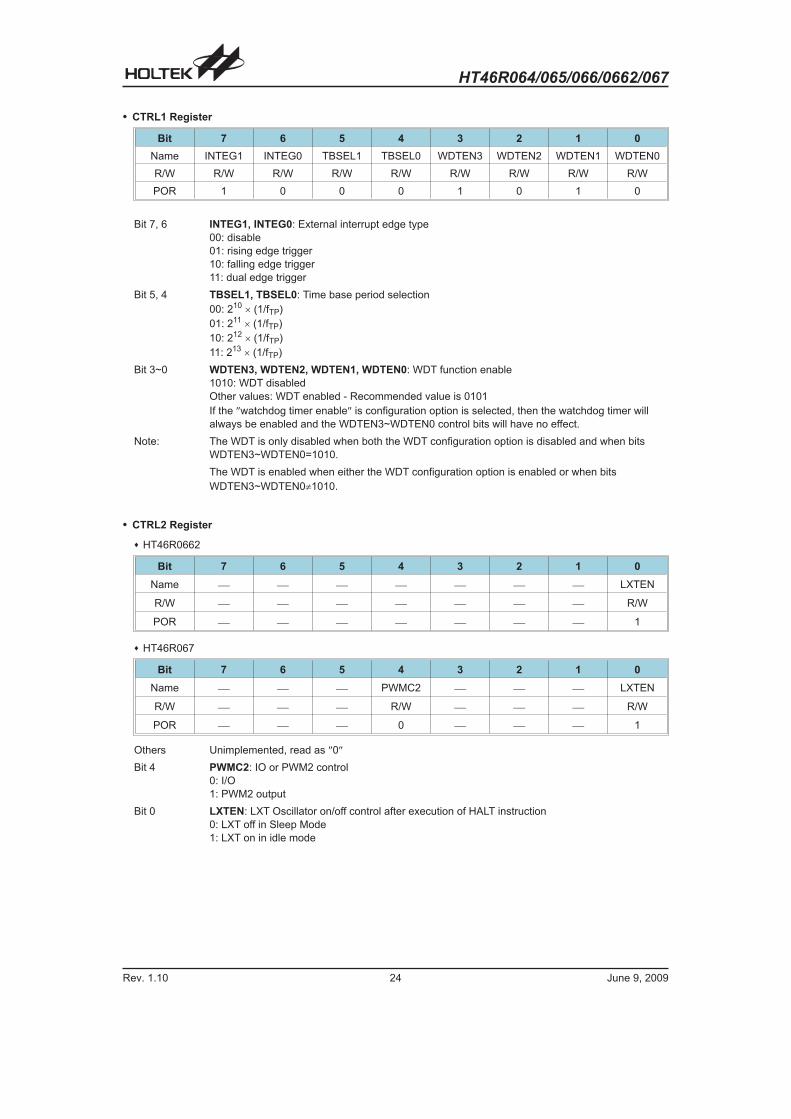
� CTRL1 Register
Bit 7 6 5 4 3 2 1 0
Name INTEG1 INTEG0 TBSEL1 TBSEL0 WDTEN3 WDTEN2 WDTEN1 WDTEN0
R/W R/W R/W R/W R/W R/W R/W R/W R/W
POR 1 0 0 0 1 0 1 0
Bit 7, 6 INTEG1, INTEG0: External interrupt edge type
00: disable
01: rising edge trigger
10: falling edge trigger
11: dual edge trigger
Bit 5, 4 TBSEL1, TBSEL0: Time base period selection
00: 210 � (1/fTP)
01: 211 � (1/fTP)
10: 212 � (1/fTP)
11: 213 � (1/fTP)
Bit 3~0 WDTEN3, WDTEN2, WDTEN1, WDTEN0: WDT function enable
1010: WDT disabled
Other values: WDT enabled - Recommended value is 0101
If the �watchdog timer enable� is configuration option is selected, then the watchdog timer will
always be enabled and the WDTEN3~WDTEN0 control bits will have no effect.
Note: The WDT is only disabled when both the WDT configuration option is disabled and when bits
WDTEN3~WDTEN0=1010.
The WDT is enabled when either the WDT configuration option is enabled or when bits
WDTEN3~WDTEN0 1010.
� CTRL2 Register
� HT46R0662
Bit 7 6 5 4 3 2 1 0
Name � � � � � � � LXTEN
R/W � � � � � � � R/W
POR � � � � � � � 1
� HT46R067
Bit 7 6 5 4 3 2 1 0
Name � � � PWMC2 � � � LXTEN
R/W � � � R/W � � � R/W
POR � � � 0 � � � 1
Others Unimplemented, read as �0�
Bit 4 PWMC2: IO or PWM2 control
0: I/O
1: PWM2 output
Bit 0 LXTEN: LXT Oscillator on/off control after execution of HALT instruction
0: LXT off in Sleep Mode
1: LXT on in idle mode

HT46R064/065/066/0662/067
Rev. 1.10 25 June 9, 2009
Wake-up Function Register � PAWK
When the microcontroller enters the Idle/Sleep Mode,
various methods exist to wake the device up and con-
tinue with normal operation. One method is to allow a
falling edge on the I/O pins to have a wake-up function.
This register is used to select which Port A I/O pins are
used to have this wake-up function.
Pull-high Registers �
PAPU, PBPU, PCPU, PDPU, PEPU, PFPU
The I/O pins, if configured as inputs, can have internal
pull-high resistors connected, which eliminates the need
for external pull-high resistors. This register selects which
I/O pins are connected to internal pull-high resistors.
Software COM Register � SCOMC
The pins PB0~PB3 on Port B can be used as SCOM
lines to drive an external LCD panel. To implement this
function, the SCOMC register is used to setup the cor-
rect bias voltages on these pins.
Oscillator
Various oscillator options offer the user a wide range of
functions according to their various application require-
ments. The flexible features of the oscillator functions
ensure that the best optimisation can be achieved in
terms of speed and power saving. Oscillator selections
and operation are selected through a combination of
configuration options and registers.
System Oscillator Overview
In addition to being the source of the main system clock
the oscillators also provide clock sources for the Watch-
dog Timer and Time Base functions. External oscillators
requiring some external components as well as a two
fully integrated internal oscillators, requiring no external
components, are provided to form a wide range of both
fast and slow system oscillators.
Type Name Freq. Pins
External Crystal HXT400kHz~
12MHz
OSC1/
OSC2
External RC ERC400kHz~
12MHzOSC1
Internal High
Speed RCHIRC 4, 8 or 12MHz �
External Low
Speed CrystalLXT 32768Hz
OSC1/
OSC2
XT1/
XT2*
Internal Low
Speed RCLIRC 13kHz �
�*� For HT46R0662/HT46R067 only
System Clock Configurations
There are five system oscillators. Three high speed os-
cillators and two low speed oscillators. The high speed
oscillators are the external crystal/ceramic oscillator -
HXT, the external - ERC, and the internal RC oscillator -
HIRC. The two low speed oscillator are the external
32768Hz oscillator - LXT and the internal 13kHz
(VDD=5V) oscillator - LIRC.
External Crystal/Resonator Oscillator � HXT
The simple connection of a crystal across OSC1 and
OSC2 will create the necessary phase shift and feed-
back for oscillation. However, for some crystals and
most resonator types, to ensure oscillation and accurate
frequency generation, it is necessary to add two small
value external capacitors, C1 and C2. The exact values
of C1 and C2 should be selected in consultation with the
crystal or resonator manufacturers specification.
Crystal Oscillator C1 and C2 Values
Crystal Frequency C1 C2
12MHz 8pF 10pF
8MHz 8pF 10pF
4MHz 8pF 10pF
1MHz 100pF 100pF
Note: C1 and C2 values are for guidance only.
Crystal Recommended Capacitor Values
� (
� &
� A
� � � � � � � :2 � � 2 8 � � �
� " # � " � $� % & ' $ $ � # � �( ' � & ) ' #
(
&
� <
. � � > ( 4 � � < � � � � � � � : : � � � � � � G 8 � � � B 4 � ( � � B � & � � � � � � � G 8 � � � B 4& 4 � � : � 3 8 ! 3 � � � � 3 C � � ( � � & � < � � � 3 � � � � � � < � � � � � � � 2� � � � 2 � < � 2 � � � 2 � � A � � � 8 B � ) < � 4
Crystal/Resonator Oscillator � HXT

HT46R064/065/066/0662/067
Rev. 1.10 26 June 9, 2009
External RC Oscillator � ERC
Using the ERC oscillator only requires that a resistor,
with a value between 24k� and 1.5M�, is connected
between OSC1 and VDD, and a capacitor is connected
between OSC and ground, providing a low cost oscilla-
tor configuration. It is only the external resistor that de-
termines the oscillation frequency; the external
capacitor has no influence over the frequency and is
connected for stability purposes only. Device trimming
during the manufacturing process and the inclusion of
internal frequency compensation circuits are used to en-
sure that the influence of the power supply voltage, tem-
perature and process variations on the oscillation
frequency are minimised. As a resistance/frequency ref-
erence point, it can be noted that with an external 120K
resistor connected and with a 5V voltage power supply
and temperature of 25 degrees, the oscillator will have a
frequency of 4MHz within a tolerance of 2%. Here only
the OSC1 pin is used, which is shared with I/O pin PA6,
leaving pin PA5 free for use as a normal I/O pin.
Internal RC Oscillator � HIRC
The internal RC oscillator is a fully integrated system os-
cillator requiring no external components. The internal
RC oscillator has three fixed frequencies of either
4MHz, 8MHz or 12MHz. Device trimming during the
manufacturing process and the inclusion of internal fre-
quency compensation circuits are used to ensure that
the influence of the power supply voltage, temperature
and process variations on the oscillation frequency are
minimised. As a result, at a power supply of either 3V or
5V and at a temperature of 25 degrees, the fixed oscilla-
tion frequency of 4MHz, 8MHz or 12MHz will have a tol-
erance within 2%. Note that if this internal system clock
option is selected, as it requires no external pins for its
operation, I/O pins PA5 and PA6 are free for use as nor-
mal I/O pins.
External 32768Hz Crystal Oscillator � LXT
When the microcontroller enters the Idle/Sleep Mode,
the system clock is switched off to stop microcontroller
activity and to conserve power. However, in many
microcontroller applications it may be necessary to keep
the internal timers operational even when the
microcontroller is in the Power-down Mode. To do this,
another clock, independent of the system clock, must be
provided. To do this a configuration option exists to allow
a high speed oscillator to be used in conjunction with a a
low speed oscillator, known as the LXT oscillator. The
LXT oscillator is implemented using a 32768Hz crystal
connected to pins OSC1/OSC2 for the HT46R064/
HT46R065/HT46R066 or connected to pins XT1/XT2
for the HT46R0662/HT46R067. However, for some
crystals, to ensure oscillation and accurate frequency
generation, it is necessary to add two small value exter-
nal capacitors, C1 and C2. The exact values of C1 and
C2 should be selected in consultation with the crystal or
resonator manufacturers specification. The external
parallel feedback resistor, Rp, is required. For the
HT46R064/HT46R065/HT46R066 devices the LXT os-
cillator must be used together with the HIRC oscillator.
For the HT46R0662/HT46R067 devices the LXT oscilla-
tor must be used together with either the HXT, ERC or
HIRC register.
LXT Oscillator C1 and C2 Values
Crystal Frequency C1 C2
32768Hz 8pF 10pF
Note: 1. C1 and C2 values are for guidance only.
2. RP=5M~10M� is recommended.
32768 Hz Crystal Recommended Capacitor Values
For the HT46R0662/HT46R067, a configuration option
determines if the XT1/XT2 pins are used for the LXT os-
cillator or as I/O pins.
� If the I/O option is selected then the XT1/XT2 pins can
be used as normal I/O pins.
� If the �LXT oscillator�is selected then the 32kHz crys-
tal should be connected to the XT1/ XT2 pins.
� � ' � � (
# ) $ < �
+ � �
� �
� � % � � &
External RC Oscillator � ERC
� � % � � � ' � 8 � � B � � � � � � � : � � � � �. � � >
� � � � � : � � � � 2 � : : � � �
� � % � � &
� � ' � � (
Internal RC Oscillator � HIRC
� � � � � � � :2 � � 2 8 � � �
� " # � " � $� % & ' $ $ � # � �( ' � & ) ' #
(
&
� <
. � � > ( 4 � � < ? � ( � � B � & � � � � � � � G 8 � � � B 4& 4 � � : � 3 8 ! 3 � � � � 3 C � < � � � 3 � � � � �� � � � < � � � � � � � 2 � 2 � < � 2 � � � 2 � � A � � � 8 B � ) < � 4
� � � � � : � � � � 2 � : : � � �
, & ) ' � @ H
External LXT Oscillator � HXT

HT46R064/065/066/0662/067
Rev. 1.10 27 June 9, 2009
LXT Oscillator Low Power Function
The LXT oscillator can function in one of two modes, the
Quick Start Mode and the Low Power Mode. The mode
selection is executed using the LXTLP bit in the CTRL0
register.
LXTLP Bit LXT Mode
0 Quick Start
1 Low-power
After power on the LXTLP bit will be automatically
cleared to zero ensuring that the LXT oscillator is in the
Quick Start operating mode. In the Quick Start Mode the
LXT oscillator will power up and stabilise quickly. How-
ever, after the LXT oscillator has fully powered up it can
be placed into the Low-power mode by setting the
LXTLP bit high. The oscillator will continue to run but
with reduced current consumption, as the higher current
consumption is only required during the LXT oscillator
start-up. In power sensitive applications, such as battery
applications, where power consumption must be kept to
a minimum, it is therefore recommended that the appli-
cation program sets the LXTLP bit high about 2 seconds
after power-on.
It should be noted that, no matter what condition the
LXTLP bit is set to, the LXT oscillator will always func-
tion normally, the only difference is that it will take more
time to start up if in the Low-power mode.
Internal Low Speed Oscillator � LIRC
The LIRC is a fully self-contained free running on-chip
RC oscillator with a typical frequency of 13kHz at 5V re-
quiring no external components. When the device en-
ters the Idle/Sleep Mode, the system clock will stop
running but the WDT oscillator continues to free-run and
to keep the watchdog active. However, to preserve
power in certain applications the LIRC can be disabled
via a configuration option.
Operating Modes
By using the LXT low frequency oscillator in combina-
tion with a high frequency oscillator, the system can be
selected to operate in a number of different modes.
These Modes are Normal, Slow, Idle and Sleep.
Mode Types and Selection
The higher frequency oscillators provide higher perfor-
mance but carry with it the disadvantage of higher
power requirements, while the opposite is of course true
for the lower frequency oscillators. With the capability of
dynamically switching between fast and slow oscillators,
the device has the flexibility to optimise the perfor-
mance/power ratio, a feature especially important in
power sensitive portable applications.
� HT46R064/HT46R065/HT46R066
For these devices, if the LXT oscillator is used then
the internal RC oscillator, HIRC, must be used as the
high frequency oscillator. If the HXT or the ERC oscil-
lator is chosen as the high frequency system clock
then the LXT oscillator cannot be used for sharing the
same pins. The CLKMOD bit in the CTRL0 register
can be used to switch the system clock from the high
speed HIRC oscillator to the low speed LXT oscillator.
When the HALT instruction is executed and the device
enters the Idle/Sleep Mode the LXT oscillator will al-
ways continue to run. For these devices the LXT crys-
tal is connected to the OSC1/OSC2 pins and LXT will
always run (the LXTEN bit is not used).
Note that CLKMOD is only valid in HIRC+LXT oscillator
configuration for HT46R064/HT46R065/HT46R066.
� HT46R0662/HT46R067
For these devices the LXT oscillator can run together
with any of the high speed oscillators, namely the
HXT, ERC or the HIRC. The CLKMOD bit in the
CTRL0 register can be used to switch the system
clock from the selected high speed oscillator to the
low speed LXT oscillator. When the HALT instruction
is executed the LXT oscillator can be chosen to run or
not using the LXTEN bit in the CTRL2 register.
@ 1 �
* �
@ � �
� � 1
A � ! 8 � � � � � < � �
� 1 �
� � 1
5 � � � 6
5 . � � � : 6
� � � � � 1 � � C � � 2 3 B ! � � � � � �
A @ 1 �
A * �
A @ � �
A � 1 �
A � � �
A =
A = � #
� F � � �5 � � � � � � � � � . � � � : �
: C � � B � 6
A � ! 8 � � � � � < � �
System Clock Configurations

HT46R064/065/066/0662/067
Rev. 1.10 28 June 9, 2009
For all devices, when the system enters the Sleep or Idle Mode, the high frequency system clock will always stop run-
ning. The accompanying tables shows the relationship between the CLKMOD bit, the HALT instruction and the
high/low frequency oscillators. The CLMOD bit can change normal or Slow Mode.
� Operating Mode Control
� HT46R064/HT46R065/HT46R066
Operating
Mode
OSC1/OSC2 Configuration
HXT ERC HIRCHIRC + LXT
HIRC LXT
Normal Run Run Run Run Run
Slow � � � Stop Run
Sleep Stop Stop Stop Stop Run
��� unimplemented
� HT46R0662/HT46R067
Operating
Mode
OSC1/OSC2 ConfigurationXT1/XT2
Configuration
HXT ERC HIRCLXT
LXTEN=0 LXTEN=1
Normal Run Run Run Run Run
Slow Stop Stop Stop Run Run
Idle Stop Stop Stop Stop Run
Sleep Stop Stop Stop Stop Stop

HT46R064/065/066/0662/067
Rev. 1.10 29 June 9, 2009
Mode Switching
The devices are switched between one mode and an-
other using a combination of the CLKMOD bit in the
CTRL0 register and the HALT instruction. The CLKMOD
bit chooses whether the system runs in either the Nor-
mal or Slow Mode by selecting the system clock to be
sourced from either a high or low frequency oscillator.
The HALT instruction forces the system into either the
Idle or Sleep Mode, depending upon whether the LXT
oscillator is running or not. The HALT instruction oper-
ates independently of the CLKMOD bit condition.
When a HALT instruction is executed and the LXT oscil-
lator is not running, the system enters the Sleep mode
the following conditions exist:
� The system oscillator will stop running and the appli-
cation program will stop at the �HALT� instruction.
� The Data Memory contents and registers will maintain
their present condition.
� The WDT will be cleared and resume counting if the
WDT clock source is selected to come from the WDT
or LXT oscillator. The WDT will stop if its clock source
originates from the system clock.
� The I/O ports will maintain their present condition.
� In the status register, the Power Down flag, PDF, will
be set and the Watchdog time-out flag, TO, will be
cleared.
Standby Current Considerations
As the main reason for entering the Idle/Sleep Mode is
to keep the current consumption of the MCU to as low a
value as possible, perhaps only in the order of several
micro-amps, there are other considerations which must
also be taken into account by the circuit designer if the
power consumption is to be minimised.
Special attention must be made to the I/O pins on the
device. All high-impedance input pins must be con-
nected to either a fixed high or low level as any floating
input pins could create internal oscillations and result in
increased current consumption. Care must also be
taken with the loads, which are connected to I/O pins,
which are setup as outputs. These should be placed in a
condition in which minimum current is drawn or con-
nected only to external circuits that do not draw current,
such as other CMOS inputs.
If the configuration options have enabled the Watchdog
Timer internal oscillator LIRC then this will continue to
run when in the Idle/Sleep Mode and will thus consume
some power. For power sensitive applications it may be
therefore preferable to use the system clock source for
the Watchdog Timer. The LXT, if configured for use, will
also consume a limited amount of power, as it continues
to run when the device enters the Idle/Sleep Mode. To
keep the LXT power consumption to a minimum level
the LXTLP bit in the CTRL0 register, which controls the
low power function, should be set high.
Wake-up
After the system enters the Idle/Sleep Mode, it can be
woken up from one of various sources listed as follows:
� An external reset
� An external falling edge on PA0 to PA7
� A system interrupt
� A WDT overflow
If the system is woken up by an external reset, the de-
vice will experience a full system reset, however, if the
device is woken up by a WDT overflow, a Watchdog
Timer reset will be initiated. Although both of these
wake-up methods will initiate a reset operation, the ac-
tual source of the wake-up can be determined by exam-
ining the TO and PDF flags. The PDF flag is cleared by a
system power-up or executing the clear Watchdog
Timer instructions and is set when executing the �HALT�instruction. The TO flag is set if a WDT time-out occurs,
and causes a wake-up that only resets the Program
Counter and Stack Pointer, the other flags remain in
their original status.
Pins PA0 to PA7 can be setup via the PAWUK register to
permit a negative transition on the pin to wake-up the
system. When a PA0 to PA7 pin wake-up occurs, the pro-
gram will resume execution at the instruction following
the �HALT� instruction.
If the system is woken up by an interrupt, then two possi-
ble situations may occur. The first is where the related
interrupt is disabled or the interrupt is enabled but the
stack is full, in which case the program will resume exe-
cution at the instruction following the �HALT� instruction.
In this situation, the interrupt which woke-up the device
will not be immediately serviced, but will rather be ser-
viced later when the related interrupt is finally enabled or
when a stack level becomes free. The other situation is
where the related interrupt is enabled and the stack is
not full, in which case the regular interrupt response
takes place. If an interrupt request flag is set to �1� be-
fore entering the Idle/Sleep Mode, then any future inter-
rupt requests will not generate a wake-up function of the
related interrupt will be ignored.

HT46R064/065/066/0662/067
Rev. 1.10 30 June 9, 2009
No matter what the source of the wake-up event is, once
a wake-up event occurs, there will be a time delay be-
fore normal program execution resumes. Consult the ta-
ble for the related time.
Wake-up
Source
Oscillator Type
ERC, IRC Crystal
External RES tRSDT + tSST1 tRSDT + tSST2
PA Port
tSST1 tSST2Interrupt
WDT Overflow
Note: 1. tRSTD (reset delay time), tSYS (system clock)
2. tRSTD is power-on delay, typical time=100ms
3. tSST1= 2 or 1024 tSYS
4. tSST2= 1024 tSYS
Wake-up Delay Time
Watchdog Timer
The Watchdog Timer, also known as the WDT, is pro-
vided to inhibit program malfunctions caused by the pro-
gram jumping to unknown locations due to certain
uncontrollable external events such as electrical noise.
Watchdog Timer Operation
It operates by providing a device reset when the Watch-
dog Timer counter overflows. Note that if the Watchdog
Timer function is not enabled, then any instructions re-
lated to the Watchdog Timer will result in no operation.
Setting up the various Watchdog Timer options are con-
trolled via the configuration options and two internal reg-
isters WDTS and CTRL1. Enabling the Watchdog Timer
can be controlled by both a configuration option and the
WDTEN bits in the CTRL1 internal register in the Data
Memory.
Configuration
Option
CTRL1
Register
WDT
Function
Disable Disable OFF
Disable Enable ON
Enable x ON
Watchdog Timer On/Off Control
The Watchdog Timer wi l l be disabled i f bi ts
WDTEN3~WDTEN0 in the CTRL1 register are written
with the binary value 1010B and WDT configuration op-
tion is disable. This will be the condition when the device
is powered up. Although any other data written to
WDTEN3~WDTEN0 will ensure that the Watchdog
Timer is enabled, for maximum protection it is recom-
mended that the value 0101B is written to these bits.
The Watchdog Timer clock can emanate from three dif-
ferent sources, selected by configuration option. These
are LXT, fSYS/4, or LIRC. It is important to note that when
the system enters the Idle/Sleep Mode the instruction
clock is stopped, therefore if the configuration options
have selected fSYS/4 as the Watchdog Timer clock
source, the Watchdog Timer will cease to function. For
systems that operate in noisy environments, using the
LIRC or the LXT as the clock source is therefore the rec-
ommended choice. The division ratio of the prescaler is
determined by bits 0, 1 and 2 of the WDTS register,
known as WS0, WS1 and WS2. If the Watchdog Timer in-
ternal clock source is selected and with the WS0, WS1
and WS2 bits of the WDTS register all set high, the
prescaler division ratio will be 1:128, which will give a
maximum time-out period.
Under normal program operation, a Watchdog Timer
time-out will initialise a device reset and set the status bit
TO. However, if the system is in the Idle/Sleep Mode,
when a Watchdog Timer time-out occurs, the device will
be woken up, the TO bit in the status register will be set
and only the Program Counter and Stack Pointer will be
reset. Three methods can be adopted to clear the con-
tents of the Watchdog Timer. The first is an external
hardware reset, which means a low level on the external
reset pin, the second is using the Clear Watchdog Timer
software instructions and the third is when a HALT in-
struction is executed. There are two methods of using
software instructions to clear the Watchdog Timer, one
of which must be chosen by configuration option. The
first option is to use the single �CLR WDT� instruction
while the second is to use the two commands �CLR
WDT1� and �CLR WDT2�. For the first option, a simple
execution of �CLR WDT� will clear the Watchdog Timer
while for the second option, both �CLR WDT1� and
�CLR WDT2� must both be executed to successfully
clear the Watchdog Timer. Note that for this second op-
tion, if �CLR WDT1� is used to clear the Watchdog
Timer, successive executions of this instruction will have
no effect, only the execution of a �CLR WDT2� instruc-
tion will clear the Watchdog Timer. Similarly after the
�CLR WDT2� instruction has been executed, only a suc-
cessive �CLR WDT1� instruction can clear the Watch-
dog Timer.
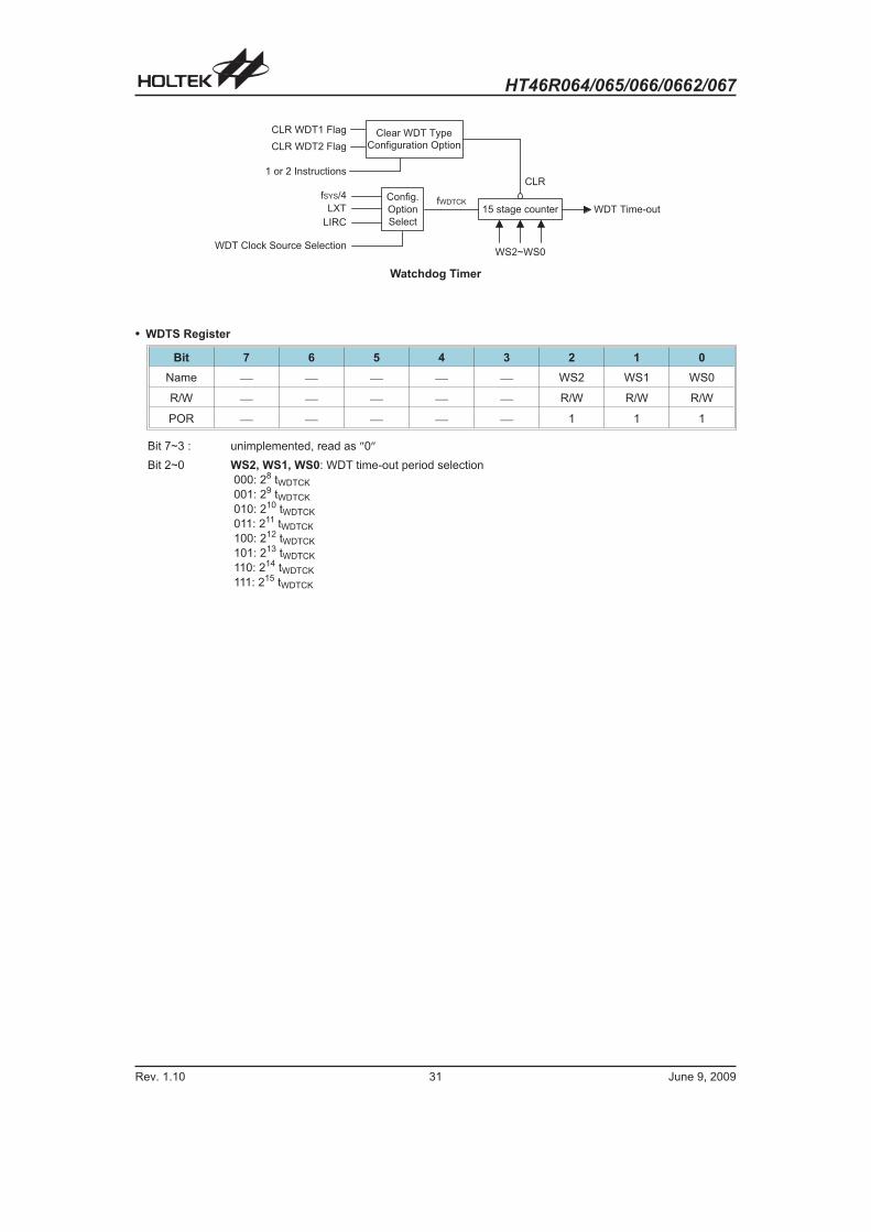
HT46R064/065/066/0662/067
Rev. 1.10 31 June 9, 2009
� WDTS Register
Bit 7 6 5 4 3 2 1 0
Name � � � � � WS2 WS1 WS0
R/W � � � � � R/W R/W R/W
POR � � � � � 1 1 1
Bit 7~3 : unimplemented, read as �0�
Bit 2~0 WS2, WS1, WS0: WDT time-out period selection
000: 28 tWDTCK
001: 29 tWDTCK
010: 210 tWDTCK
011: 211 tWDTCK
100: 212 tWDTCK
101: 213 tWDTCK
110: 214 tWDTCK
111: 215 tWDTCK
( % � � � � ! � � 2 8 � � � � � � � � � � � � 8 �
� & D � $
A � ! 4
� < � �
� : � 2 �
� � � � : 2 ; � 8 � 2 � � � : � 2 � �
: � � � � � � � � � � < �
A � ! 8 � � � � � � < � �
� � � � � � ( � � : � !
� � � � � � & � � : � !
( � � � & � � � � � 8 2 � � � � � �
A = � #
� � �
� 1 �A � � � F
Watchdog Timer

HT46R064/065/066/0662/067
Rev. 1.10 32 June 9, 2009
Reset and Initialisation
A reset function is a fundamental part of any
microcontroller ensuring that the device can be set to
some predetermined condition irrespective of outside
parameters. The most important reset condition is after
power is first applied to the microcontroller. In this case,
internal circuitry will ensure that the microcontroller, af-
ter a short delay, will be in a well defined state and ready
to execute the first program instruction. After this
power-on reset, certain important internal registers will
be set to defined states before the program com-
mences. One of these registers is the Program Counter,
which will be reset to zero forcing the microcontroller to
begin program execution from the lowest Program
Memory address.
In addition to the power-on reset, situations may arise
where it is necessary to forcefully apply a reset condition
when the microcontroller is running. One example of this
is where after power has been applied and the
microcontroller is already running, the RES line is force-
fully pulled low. In such a case, known as a normal oper-
ation reset, some of the microcontroller registers remain
unchanged allowing the microcontroller to proceed with
normal operation after the reset line is allowed to return
high. Another type of reset is when the Watchdog Timer
overflows and resets the microcontroller. All types of re-
set operations result in different register conditions be-
ing setup.
Another reset exists in the form of a Low Voltage Reset,
LVR, where a full reset, similar to the RES reset is imple-
mented in situations where the power supply voltage
falls below a certain threshold.
Reset Functions
There are five ways in which a microcontroller reset can
occur, through events occurring both internally and ex-
ternally:
� Power-on Reset
The most fundamental and unavoidable reset is the
one that occurs after power is first applied to the
microcontroller. As well as ensuring that the Program
Memory begins execution from the first memory ad-
dress, a power-on reset also ensures that certain
other registers are preset to known conditions. All the
I/O port and port control registers will power up in a
high condition ensuring that all pins will be first set to
inputs.
Although the microcontroller has an internal RC reset
function, if the VDD power supply rise time is not fast
enough or does not stabilise quickly at power-on, the
internal reset function may be incapable of providing
proper reset operation. For this reason it is recom-
mended that an external RC network is connected to
the RES pin, whose additional time delay will ensure
that the RES pin remains low for an extended period
to allow the power supply to stabilise. During this time
delay, normal operation of the microcontroller will be
inhibited. After the RES line reaches a certain voltage
value, the reset delay time tRSTD is invoked to provide
an extra delay time after which the microcontroller will
begin normal operation. The abbreviation SST in the
figures stands for System Start-up Timer.
For most applications a resistor connected between
VDD and the RES pin and a capacitor connected be-
tween VSS and the RES pin will provide a suitable ex-
ternal reset circuit. Any wiring connected to the RES
pin should be kept as short as possible to minimise
any stray noise interference.
For applications that operate within an environment
where more noise is present the Enhanced Reset Cir-
cuit shown is recommended.
More information regarding external reset circuits is
located in Application Note HA0075E on the Holtek
website.
� *
+ � �
� � � � � : � � � � � �
$ 4 - � + � �
� � � � � 9 � � �� � � � � 9 � � �
Note: tRSTD is power-on delay, typical time=100ms
Power-On Reset Timing Chart
� * � � � )
$ 4 ( D ( � �
( $ ; � D
( $ $ ; �
+ � �
+
$ 4 $ ( � � I I
+ � �
( . # ( # � I
, $ $ � I
Note: �*� It is recommended that this component is
added for added ESD protection
�**� It is recommended that this component is
added in environments where power line noise
is significant
External RES Circuit
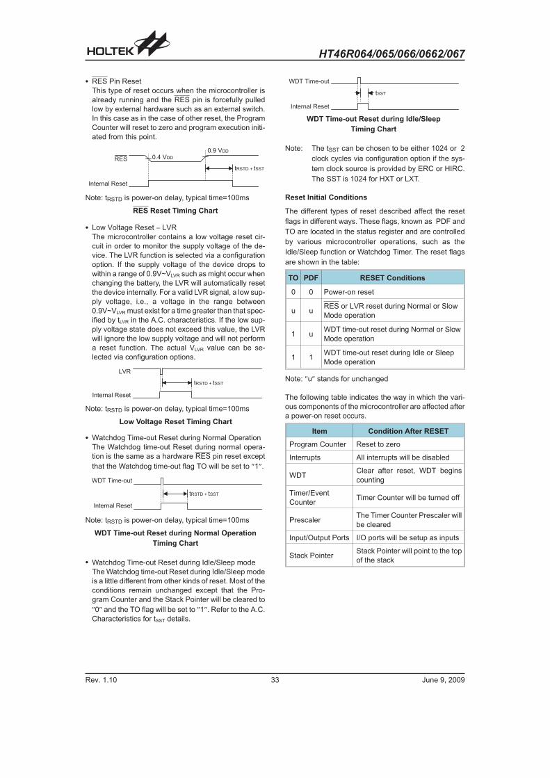
HT46R064/065/066/0662/067
Rev. 1.10 33 June 9, 2009
� RES Pin Reset
This type of reset occurs when the microcontroller is
already running and the RES pin is forcefully pulled
low by external hardware such as an external switch.
In this case as in the case of other reset, the Program
Counter will reset to zero and program execution initi-
ated from this point.
� Low Voltage Reset � LVR
The microcontroller contains a low voltage reset cir-
cuit in order to monitor the supply voltage of the de-
vice. The LVR function is selected via a configuration
option. If the supply voltage of the device drops to
within a range of 0.9V~VLVR such as might occur when
changing the battery, the LVR will automatically reset
the device internally. For a valid LVR signal, a low sup-
ply voltage, i.e., a voltage in the range between
0.9V~VLVR must exist for a time greater than that spec-
ified by tLVR in the A.C. characteristics. If the low sup-
ply voltage state does not exceed this value, the LVR
will ignore the low supply voltage and will not perform
a reset function. The actual VLVR value can be se-
lected via configuration options.
� Watchdog Time-out Reset during Normal Operation
The Watchdog time-out Reset during normal opera-
tion is the same as a hardware RES pin reset except
that the Watchdog time-out flag TO will be set to �1�.
� Watchdog Time-out Reset during Idle/Sleep mode
The Watchdog time-out Reset during Idle/Sleep mode
is a little different from other kinds of reset. Most of the
conditions remain unchanged except that the Pro-
gram Counter and the Stack Pointer will be cleared to
�0� and the TO flag will be set to �1�. Refer to the A.C.
Characteristics for tSST details.
Note: The tSST can be chosen to be either 1024 or 2
clock cycles via configuration option if the sys-
tem clock source is provided by ERC or HIRC.
The SST is 1024 for HXT or LXT.
Reset Initial Conditions
The different types of reset described affect the reset
flags in different ways. These flags, known as PDF and
TO are located in the status register and are controlled
by various microcontroller operations, such as the
Idle/Sleep function or Watchdog Timer. The reset flags
are shown in the table:
TO PDF RESET Conditions
0 0 Power-on reset
u uRES or LVR reset during Normal or Slow
Mode operation
1 uWDT time-out reset during Normal or Slow
Mode operation
1 1WDT time-out reset during Idle or Sleep
Mode operation
Note: �u� stands for unchanged
The following table indicates the way in which the vari-
ous components of the microcontroller are affected after
a power-on reset occurs.
Item Condition After RESET
Program Counter Reset to zero
Interrupts All interrupts will be disabled
WDTClear after reset, WDT begins
counting
Timer/Event
CounterTimer Counter will be turned off
PrescalerThe Timer Counter Prescaler will
be cleared
Input/Output Ports I/O ports will be setup as inputs
Stack PointerStack Pointer will point to the top
of the stack
� *
� � � � � : � � � � � �
$ 4 - � + � �
$ 4 # � + � �
� � � � � 9 � � �
Note: tRSTD is power-on delay, typical time=100ms
RES Reset Timing Chart
� + �
� � � � � : � � � � � �
� � � � � 9 � � �
Note: tRSTD is power-on delay, typical time=100ms
Low Voltage Reset Timing Chart
� � � � � 9 � � �
� � � � � � � � � 8 �
� � � � � : � � � � � �
Note: tRSTD is power-on delay, typical time=100ms
WDT Time-out Reset during Normal Operation
Timing Chart
� �
� � � � � � � � � 8 �
� � � � � : � � � � � �
WDT Time-out Reset during Idle/Sleep
Timing Chart

HT46R064/065/066/0662/067
Rev. 1.10 34 June 9, 2009
The different kinds of resets all affect the internal registers of the microcontroller in different ways. To ensure reliable
continuation of normal program execution after a reset occurs, it is important to know what condition the microcontroller
is in after a particular reset occurs. The following table describes how each type of reset affects each of the
microcontroller internal registers.
RegisterPower-on
Reset
RES or LVR
Reset
WDT Time-out
(Normal Operation)
WDT Time-out
(Idle/Sleep)
PCL � � � � � 0 0 0 0 0 0 0 0 0 0 0 0 0 0 0 0 0 0 0 0 0 0 0 0 0 0 0 0 0 0 0 0
MP0 � 1 x x x x x x x 1 u u u u u u u 1 u u u u u u u 1 u u u u u u u
MP1 � 1 x x x x x x x 1 u u u u u u u 1 u u u u u u u 1 u u u u u u u
MP0 � � � � x x x x x x x x u u u u u u u u u u u u u u u u u u u u u u u u
MP1 � � � � x x x x x x x x u u u u u u u u u u u u u u u u u u u u u u u u
BP � � � � � � � � � 0 � � � � � � � 0 � � � � � � � 0 � � � � � � � u
ACC � � � � � x x x x x x x x u u u u u u u u u u u u u u u u u u u u u u u u
TBLP � � � � � x x x x x x x x u u u u u u u u u u u u u u u u u u u u u u u u
TBLH
� � � x x x x x x � � u u u u u u � � u u u u u u � � u u u u u u
� � � � x x x x x x x � u u u u u u u � u u u u u u u � u u u u u u u
� x x x x x x x x u u u u u u u u u u u u u u u u u u u u u u u u
WDTS � � � � � � � � � � 1 1 1 � � � � � 1 1 1 � � � � � 1 1 1 � � � � � u u u
STATUS � � � � � � � 0 0 x x x x � � u u u u u u � � 1 u u u u u � � 1 1 u u u u
INTC0 � � � � � � 0 0 0 0 0 0 0 � 0 0 0 0 0 0 0 � 0 0 0 0 0 0 0 � u u u u u u u
INTC1
� � � � 0 � � � 0 � � � 0 � � � 0 � � � 0 � � � 0 � � � u � � � u
� � � � � 0 0 � � 0 0 � � 0 0 � � 0 0 � � 0 0 � � 0 0 � � u u � � u u
� � 0 0 0 � 0 0 0 � 0 0 0 � 0 0 0 � 0 0 0 � 0 0 0 � u u u � u u u
TMR0 � � � � � x x x x x x x x x x x x x x x x x x x x x x x x u u u u u u u u
TMR0C � � � � � 0 0 0 0 1 0 0 0 0 0 0 0 1 0 0 0 0 0 0 0 1 0 0 0 u u u u u u u u
TMR1 � � � � x x x x x x x x x x x x x x x x x x x x x x x x u u u u u u u u
TMR1C � � � � 0 0 0 0 1 � � � 0 0 0 0 1 � � � 0 0 0 0 1 � � � u u u u u � � �
TMR2 � x x x x x x x x x x x x x x x x x x x x x x x x u u � u u u u u
TMR2C � 0 0 � 0 1 0 0 0 0 0 � 0 1 0 0 0 0 0 � 0 1 0 0 0 u u u u u u u u
PA � � � � � 1 1 1 1 1 1 1 1 1 1 1 1 1 1 1 1 1 1 1 1 1 1 1 1 u u u u u u u u
PAC � � � � � 1 1 1 1 1 1 1 1 1 1 1 1 1 1 1 1 1 1 1 1 1 1 1 1 u u u u u u u u
PAWK � � � � � 0 0 0 0 0 0 0 0 0 0 0 0 0 0 0 0 0 0 0 0 0 0 0 0 u u u u u u u u
PAPU � � � � � � 0 0 0 0 0 0 0 � 0 0 0 0 0 0 0 � 0 0 0 0 0 0 0 � u u u u u u u
PB � � � � � 1 1 1 1 1 1 � � 1 1 1 1 1 1 � � 1 1 1 1 1 1 � � u u u u u u
PBC � � � � � 1 1 1 1 1 1 � � 1 1 1 1 1 1 � � 1 1 1 1 1 1 � � u u u u u u
PBPU � � � � � 0 0 0 0 0 0 � 0 0 0 0 0 0 0 � 0 0 0 0 0 0 0 � � u u u u u u
PB � � 1 1 1 1 1 1 1 1 1 1 1 1 1 1 1 1 1 1 1 1 1 1 1 1 u u u u u u u u
PBC � � 1 1 1 1 1 1 1 1 1 1 1 1 1 1 1 1 1 1 1 1 1 1 1 1 u u u u u u u u
PBPU � � 0 0 0 0 0 0 0 0 0 0 0 0 0 0 0 0 0 0 0 0 0 0 0 0 u u u u u u u u
HT
46R
064
HT
46R
065
HT
46R
066
HT
46R
0662
HT
46R
067

HT46R064/065/066/0662/067
Rev. 1.10 35 June 9, 2009
RegisterPower-on
Reset
RES or LVR
Reset
WDT Time-out
(Normal Operation)
WDT Time-out
(Idle/Sleep)
PC � � � � � 1 1 1 1 � � � � 1 1 1 1 � � � � 1 1 1 1 � � � � u u u u
PCC � � � � � 1 1 1 1 � � � � 1 1 1 1 � � � � 1 1 1 1 � � � � u u u u
PCPU � � � � � 0 0 0 0 � � � � 0 0 0 0 � � � � 0 0 0 0 � � � � u u u u
PC � � � � 1 1 1 1 1 1 1 1 1 1 1 1 1 1 1 1 1 1 1 1 1 1 1 1 u u u u u u u u
PCC � � � � 1 1 1 1 1 1 1 1 1 1 1 1 1 1 1 1 1 1 1 1 1 1 1 1 u u u u u u u u
PCPU � � � � 0 0 0 0 0 0 0 0 0 0 0 0 0 0 0 0 0 0 0 0 0 0 0 0 u u u u u u u u
PD � � � � � 1 1 1 1 � � � � 1 1 1 1 � � � � 1 1 1 1 � � � � u u u u
PDC � � � � � 1 1 1 1 � � � � 1 1 1 1 � � � � 1 1 1 1 � � � � u u u u
PDPU � � � � � 0 0 0 0 � � � � 0 0 0 0 � � � � 0 0 0 0 � � � � u u u u
PD � � 1 1 1 1 1 1 1 1 1 1 1 1 1 1 1 1 1 1 1 1 1 1 1 1 u u u u u u u u
PDC � � 1 1 1 1 1 1 1 1 1 1 1 1 1 1 1 1 1 1 1 1 1 1 1 1 u u u u u u u u
PDPU � � 0 0 0 0 0 0 0 0 0 0 0 0 0 0 0 0 0 0 0 0 0 0 0 0 u u u u u u u u
PE � � 1 1 1 1 1 1 1 1 1 1 1 1 1 1 1 1 1 1 1 1 1 1 1 1 u u u u u u u u
PEC � � 1 1 1 1 1 1 1 1 1 1 1 1 1 1 1 1 1 1 1 1 1 1 1 1 u u u u u u u u
PEPU � � 0 0 0 0 0 0 0 0 0 0 0 0 0 0 0 0 0 0 0 0 0 0 0 0 u u u u u u u u
PF � � � � � � � � 1 1 � � � � � � 1 1 � � � � � � 1 1 � � � � � � u u
PFC � � � � � � � � 1 1 � � � � � � 1 1 � � � � � � 1 1 � � � � � � u u
PFPU � � � � � � � � 0 0 � � � � � � 0 0 � � � � � � 0 0 � � � � � � u u
CTRL0
� � � 0 � 0 0 0 0 � � 0 � 0 0 0 0 � � 0 � 0 0 0 0 � � u � u u u u
� � 0 0 � 0 0 0 0 � 0 0 � 0 0 0 0 � 0 0 � 0 0 0 0 � u u � u u u u
� � � 0 0 0 0 0 0 0 0 0 0 0 0 0 0 0 0 0 0 0 0 0 0 0 0 u u u u u u u u
CTRL1 � � � � � 1 0 0 0 1 0 1 0 1 0 0 0 1 0 1 0 1 0 0 0 1 0 1 0 u u u u u u u u
CTRL2� � � � � � � � 1 � � � � � � � 1 � � � � � � � 1 � � � � � � � u
� � � � 0 � � � 1 � � � 0 � � � 1 � � � 0 � � � 1 � � � u � � � u
SCOMC � � � � 0 0 0 0 0 0 0 0 0 0 0 0 0 0 0 0 0 0 0 0 0 0 0 0 u u u u u u u u
PWM0 � � � � � x x x x x x x x x x x x x x x x x x x x x x x x u u u u u u u u
PWM1 � � � x x x x x x x x x x x x x x x x x x x x x x x x u u u u u u u u
PWM2 � x x x x x x x x x x x x x x x x x x x x x x x x u u u u u u u u
ADRL � � � � � x x x x � � � � x x x x � � � � x x x x � � � � u u u u � � � �
ADRH � � � � � x x x x x x x x x x x x x x x x x x x x x x x x u u u u u u u u
ADCR � � � � � 0 1 0 0 0 0 0 0 0 1 0 0 0 0 0 0 0 1 0 0 0 0 0 0 u u u u u u u u
ACSR � � � � � 1 0 � � � 0 0 0 1 0 � � � 0 0 0 1 0 � � � 0 0 0 u u � � � u u u
Note: �-� not implemented
�u� means �unchanged�
�x� means �unknown�
HT
46R
064
HT
46R
065
HT
46R
066
HT
46R
0662
HT
46R
067
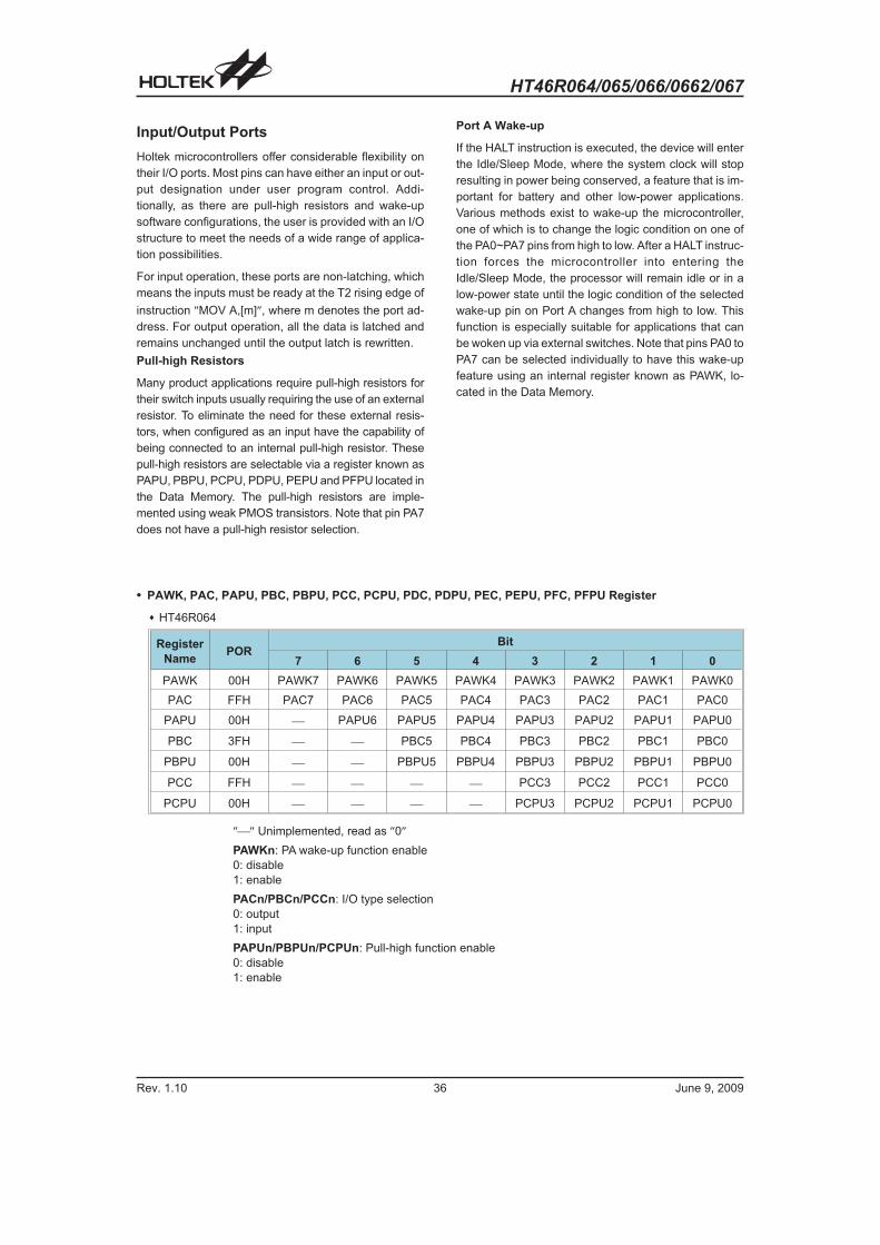
HT46R064/065/066/0662/067
Rev. 1.10 36 June 9, 2009
Input/Output Ports
Holtek microcontrollers offer considerable flexibility on
their I/O ports. Most pins can have either an input or out-
put designation under user program control. Addi-
tionally, as there are pull-high resistors and wake-up
software configurations, the user is provided with an I/O
structure to meet the needs of a wide range of applica-
tion possibilities.
For input operation, these ports are non-latching, which
means the inputs must be ready at the T2 rising edge of
instruction �MOV A,[m]�, where m denotes the port ad-
dress. For output operation, all the data is latched and
remains unchanged until the output latch is rewritten.
Pull-high Resistors
Many product applications require pull-high resistors for
their switch inputs usually requiring the use of an external
resistor. To eliminate the need for these external resis-
tors, when configured as an input have the capability of
being connected to an internal pull-high resistor. These
pull-high resistors are selectable via a register known as
PAPU, PBPU, PCPU, PDPU, PEPU and PFPU located in
the Data Memory. The pull-high resistors are imple-
mented using weak PMOS transistors. Note that pin PA7
does not have a pull-high resistor selection.
Port A Wake-up
If the HALT instruction is executed, the device will enter
the Idle/Sleep Mode, where the system clock will stop
resulting in power being conserved, a feature that is im-
portant for battery and other low-power applications.
Various methods exist to wake-up the microcontroller,
one of which is to change the logic condition on one of
the PA0~PA7 pins from high to low. After a HALT instruc-
tion forces the microcontroller into entering the
Idle/Sleep Mode, the processor will remain idle or in a
low-power state until the logic condition of the selected
wake-up pin on Port A changes from high to low. This
function is especially suitable for applications that can
be woken up via external switches. Note that pins PA0 to
PA7 can be selected individually to have this wake-up
feature using an internal register known as PAWK, lo-
cated in the Data Memory.
� PAWK, PAC, PAPU, PBC, PBPU, PCC, PCPU, PDC, PDPU, PEC, PEPU, PFC, PFPU Register
� HT46R064
Register
NamePOR
Bit
7 6 5 4 3 2 1 0
PAWK 00H PAWK7 PAWK6 PAWK5 PAWK4 PAWK3 PAWK2 PAWK1 PAWK0
PAC FFH PAC7 PAC6 PAC5 PAC4 PAC3 PAC2 PAC1 PAC0
PAPU 00H � PAPU6 PAPU5 PAPU4 PAPU3 PAPU2 PAPU1 PAPU0
PBC 3FH � � PBC5 PBC4 PBC3 PBC2 PBC1 PBC0
PBPU 00H � � PBPU5 PBPU4 PBPU3 PBPU2 PBPU1 PBPU0
PCC FFH � � � � PCC3 PCC2 PCC1 PCC0
PCPU 00H � � � � PCPU3 PCPU2 PCPU1 PCPU0
��� Unimplemented, read as �0�
PAWKn: PA wake-up function enable
0: disable
1: enable
PACn/PBCn/PCCn: I/O type selection
0: output
1: input
PAPUn/PBPUn/PCPUn: Pull-high function enable
0: disable
1: enable

HT46R064/065/066/0662/067
Rev. 1.10 37 June 9, 2009
� HT46R065
Register
NamePOR
Bit
7 6 5 4 3 2 1 0
PAWK 00H PAWK7 PAWK6 PAWK5 PAWK4 PAWK3 PAWK2 PAWK1 PAWK0
PAC FFH PAC7 PAC6 PAC5 PAC4 PAC3 PAC2 PAC1 PAC0
PAPU 00H � PAPU6 PAPU5 PAPU4 PAPU3 PAPU2 PAPU1 PAPU0
PBC 3FH � � PBC5 PBC4 PBC3 PBC2 PBC1 PBC0
PBPU 00H � � PBPU5 PBPU4 PBPU3 PBPU2 PBPU1 PBPU0
PCC FFH PCC7 PCC6 PCC5 PCC4 PCC3 PCC2 PCC1 PCC0
PCPU 00H PCPU7 PCPU6 PCPU5 PCPU4 PCPU3 PCPU2 PCPU1 PCPU0
��� Unimplemented, read as �0�
PAWKn: PA wake-up function enable
0: disable
1: enable
PACn/PBCn/PCCn: I/O type selection
0: output
1: input
PAPUn/PBPUn/PCPUn: Pull-high function enable
0: disable
1: enable
� HT46R066
Register
NamePOR
Bit
7 6 5 4 3 2 1 0
PAWK 00H PAWK7 PAWK6 PAWK5 PAWK4 PAWK3 PAWK2 PAWK1 PAWK0
PAC FFH PAC7 PAC6 PAC5 PAC4 PAC3 PAC2 PAC1 PAC0
PAPU 00H � PAPU6 PAPU5 PAPU4 PAPU3 PAPU2 PAPU1 PAPU0
PBC 3FH � � PBC5 PBC4 PBC3 PBC2 PBC1 PBC0
PBPU 00H � � PBPU5 PBPU4 PBPU3 PBPU2 PBPU1 PBPU0
PCC FFH PCC7 PCC6 PCC5 PCC4 PCC3 PCC2 PCC1 PCC0
PCPU 00H PCPU7 PCPU6 PCPU5 PCPU4 PCPU3 PCPU2 PCPU1 PCPU0
PDC 0FH � � � � PDC3 PDC2 PDC1 PDC0
PDPU 00H � � � � PDPU3 PDPU2 PDPU1 PDPU0
��� Unimplemented, read as �0�
PAWKn: PA wake-up function enable
0: disable
1: enable
PACn/PBCn/PCCn/PDCn: I/O type selection
0: output
1: input
PAPUn/PBPUn/PCPUn/PDPUn: Pull-high function enable
0: disable
1: enable

HT46R064/065/066/0662/067
Rev. 1.10 38 June 9, 2009
� HT46R0662/HT46R067
Register
NamePOR
Bit
7 6 5 4 3 2 1 0
PAWK 00H PAWK7 PAWK6 PAWK5 PAWK4 PAWK3 PAWK2 PAWK1 PAWK0
PAC FFH PAC7 PAC6 PAC5 PAC4 PAC3 PAC2 PAC1 PAC0
PAPU 00H � PAPU6 PAPU5 PAPU4 PAPU3 PAPU2 PAPU1 PAPU0
PBC FFH PBC7 PBC6 PBC5 PBC4 PBC3 PBC2 PBC1 PBC0
PBPU 00H PBPU7 PBPU6 PBPU5 PBPU4 PBPU3 PBPU2 PBPU1 PBPU0
PCC FFH PCC7 PCC6 PCC5 PCC4 PCC3 PCC2 PCC1 PCC0
PCPU 00H PCPU7 PCPU6 PCPU5 PCPU4 PCPU3 PCPU2 PCPU1 PCPU0
PDC FFH PDC7 PDC6 PDC5 PDC4 PDC3 PDC2 PDC1 PDC0
PDPU 00H PDPU7 PDPU6 PDPU5 PDPU4 PDPU3 PDPU2 PDPU1 PDPU0
PEC FFH PEC7 PEC6 PEC5 PEC4 PEC3 PEC2 PEC1 PEC0
PEPU 00H PEPU7 PEPU6 PEPU5 PEPU4 PEPU3 PEPU2 PEPU1 PEPU0
PFC 03H � � � � � � PFC1 PFC0
PFPU 00H � � � � � � PFPU1 PFPU0
��� Unimplemented, read as �0�
PAWKn: PA wake-up function enable
0: disable
1: enable
PACn/PBCn/PCCn/PDCn/PECn/PFCn: I/O type selection
0: output
1: input
PAPUn/PBPUn/PCPUn/PDPUn/PEPUn/PFPUn: Pull-high function enable
0: disable
1: enable
I/O Port Control Registers
Each Port has its own control register, known as PAC,
PBC, PCC, PDC, PEC, PFC which controls the in-
put/output configuration. With this control register, each
I/O pin with or without pull-high resistors can be recon-
figured dynamically under software control. For the I/O
pin to function as an input, the corresponding bit of the
control register must be written as a �1�. This will then
allow the logic state of the input pin to be directly read by
instructions. When the corresponding bit of the control
register is written as a �0�, the I/O pin will be setup as a
CMOS output. If the pin is currently setup as an output,
instructions can still be used to read the output register.
However, it should be noted that the program will in fact
only read the status of the output data latch and not the
actual logic status of the output pin.
Pin-shared Functions
The flexibility of the microcontroller range is greatly en-
hanced by the use of pins that have more than one func-
tion. Limited numbers of pins can force serious design
constraints on designers but by supplying pins with
multi-functions, many of these difficulties can be over-
come. For some pins, the chosen function of the
multi-function I/O pins is set by configuration options
while for others the function is set by application pro-
gram control.
� External Interrupt Input
The external interrupt pin, INT, is pin-shared with an
I/O pin. To use the pin as an external interrupt input
the correct bits in the INTC0 register must be pro-
grammed. The pin must also be setup as an input by
setting the PAC3 bit in the Port Control Register. A
pull-high resistor can also be selected via the appro-
priate port pull-high resistor register. Note that even if
the pin is setup as an external interrupt input the I/O
function still remains.
� External Timer/Event Counter Input
The Timer/Event Counter pins, TC0, TC1 and TC2 are
pin-shared with I/O pins. For these shared pins to be
used as Timer/Event Counter inputs, the Timer/Event
Counter must be configured to be in the Event Coun-
ter or Pulse Width Capture Mode. This is achieved by
setting the appropriate bits in the Timer/Event Counter
Control Register. The pins must also be setup as in-
puts by setting the appropriate bit in the Port Control
Register. Pull-high resistor options can also be se-
lected using the port pull-high resistor registers. Note
that even if the pin is setup as an external timer input
the I/O function still remains.

HT46R064/065/066/0662/067
Rev. 1.10 39 June 9, 2009
� PFD Output
The PFD function output is pin-shared with an I/O pin.
The output function of this pin is chosen using the
CTRL0 register. Note that the corresponding bit of
the port control register, must setup the pin as an
output to enable the PFD output. If the port control
register has setup the pin as an input, then the pin will
function as a normal logic input with the usual
pull-high selection, even if the PFD function has been
selected.
� PWM Outputs
The PWM function whose outputs are pin-shared with
I/O pins. The PWM output functions are chosen using
the CTRL0 and CTRL2 registers. Note that the corre-
sponding bit of the port control registers, for the output
pin, must setup the pin as an output to enable the
PWM output. If the pins are setup as inputs, then the
pin will function as a normal logic input with the usual
pull-high selections, even if the PWM registers have
enabled the PWM function.
� SCOM Driver Pins
Pins PB0~PB3 on Port B can be used as LCD COM
driver pins. This function is controlled using the
SCOMC register which will generate the necessary
1/2 bias signals on these four pins.
� A/D Inputs
Each device in this series has either four or eight in-
puts to the A/D converter. All of these analog inputs
are pin-shared with I/O pins. If these pins are to be
used as A/D inputs and not as I/O pins then the corre-
sponding PCRn bits in the A/D converter control regis-
ter, ADCR, must be properly setup. There are no
configuration options associated with the A/D con-
verter. If chosen as I/O pins, then full pull-high resistor
configuration options remain, however if used as A/D
inputs then any pull-high resistor configuration options
associated with these pins will be automatically dis-
connected.
Pin Remapping Configuration �
HT46R066/HT46R0662/HT46R067
The pin remapping function enables the function pins
INT, TC0 and PFD to be located on different port pins. It
is important not to confuse the Pin Remapping function
with the Pin-shared function, these two functions have
no interdependence.
The PCFG bit in the CTRL0 register allows the three
function pins INT, TC0 and PFD to be remapped to dif-
ferent port pins. After power up, this bit will be reset to
zero, which will define the default port pins to which
these three functions will be mapped. Changing this bit
will move the functions to other port pins.
Examination of the pin names on the package diagrams
will reveal that some pin function names are repeated,
this indicates a function pin that can be remapped to
other port pins. If the pin name is bracketed then this in-
dicates its alternative location. Pin names without brack-
ets indicates its default location which is the condition
after Power-on.
PCFG Bit Status
PCFG Bit 0 1
Pin Mapping
INT/PA3
TC0/PA2
PFD/PA1
[INT]/PB5
[TC0]/PB4
[PFD]/PB3
Pin Remapping
I/O Pin Structures
The diagrams illustrate the I/O pin internal structures. As
the exact logical construction of the I/O pin may differ
from these drawings, they are supplied as a guide only
to assist with the functional understanding of the I/O
pins.
+ � �
��1
� � ; � � 8 < � � : � 2 � � � � � � � � � ; � � 8 <
� � � B � � � � � � � � ! � � � � �
� J
F
� J
F
� � : � � � �
� � � � � � 8 �
� � � � � � � � : � � � ! � � � � �
3 � < � � � � � �
� � � B � � � : � � � ! � � � � �
� � � � � � � � � � � � � ! � � � � �
� � � � � � � �
� � � � < �
J
J
� � � : �
� � � ;� 8 : : � 8 <
� 8 : : � @ � ! 3 � : � 2 �
Generic Input/Output Ports
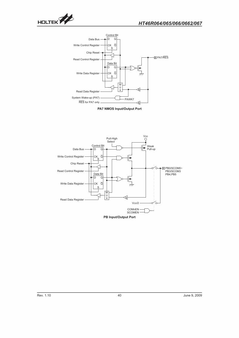
HT46R064/065/066/0662/067
Rev. 1.10 40 June 9, 2009
� � � F )
��1
� � � B � � � � � � � � ! � � � � �
� � : � � � �
� � � � � � 8 �
� � � � � � � � : � � � ! � � � � �
3 � < � � � � � �
� � � B � � � : � � � ! � � � � �
� � � � � � � � � � � � � ! � � � � �
� � � � � � � �
� J
F
J
� J
F
J
� � ) � � *
� � � � � � � � ; � � 8 < � 5 � � ) 6
� * � A � � � � ) � : �
PA7 NMOS Input/Output Port
+ � �
��1
� � � B � � � � � � � � ! � � � � �
� � : � � � �
� 8 : : � @ � ! 3� � : � 2 �
� � � � � � 8 �
� � � � � � � � : � � � ! � � � � �
3 � < � � � � � �
� � � B � � � : � � � ! � � � � �
� � � � � � � � � � � � � ! � � � � �
� � � � � � � �
� � $ � � � $ D� � , � � � ,� � # ? � � %
+ � � � &
� � � ;� 8 : : � 8 <� J
F
J
� J
F
J
� � * .
� � * .
PB Input/Output Port

HT46R064/065/066/0662/067
Rev. 1.10 41 June 9, 2009
Programming Considerations
Within the user program, one of the first things to con-
sider is port initialisation. After a reset, the I/O data reg-
ister and I/O port control register will be set high. This
means that all I/O pins will default to an input state, the
level of which depends on the other connected circuitry
and whether pull-high options have been selected. If the
port control registers, are then programmed to setup
some pins as outputs, these output pins will have an ini-
tial high output value unless the associated port data
register is first programmed. Selecting which pins are in-
puts and which are outputs can be achieved byte-wide
by loading the correct value into the port control register
or by programming individual bits in the port control reg-
ister using the �SET [m].i� and �CLR [m].i� instructions.
Note that when using these bit control instructions, a
read-modify-write operation takes place. The
microcontroller must first read in the data on the entire
port, modify it to the required new bit values and then re-
write this data back to the output ports.
Pins PA0 to PA7 each have a wake-up functions, se-
lected via the PAWK register. When the device is in the
Idle/Sleep Mode, various methods are available to wake
the device up. One of these is a high to low transition of
any of the these pins. Single or multiple pins on Port A
can be setup to have this function.
Timer/Event Counters
The provision of timers form an important part of any
microcontroller, giving the designer a means of carrying
out time related functions. The devices contain from one
to three count-up timer of 8-bit capacity. As the timers
have three different operating modes, they can be con-
figured to operate as a general timer, an external event
counter or as a pulse width capture device. The provi-
sion of an internal prescaler to the clock circuitry on
gives added range to the timers.
There are two types of registers related to the
Timer/Event Counters. The first is the register that con-
tains the actual value of the timer and into which an ini-
tial value can be preloaded. Reading from this register
retrieves the contents of the Timer/Event Counter. The
second type of associated register is the Timer Control
Register which defines the timer options and deter-
mines how the timer is to be used. The device can have
the timer clock configured to come from the internal
clock source. In addition, the timer clock source can also
be configured to come from an external timer pin.
Configuring the Timer/Event Counter Input Clock
Source
The Timer/Event Counter clock source can originate
from various sources, an internal clock or an external
pin. The internal clock source source is used when the
timer is in the timer mode or in the pulse width capture
mode. For some Timer/Event Counters, this internal
clock source is first divided by a prescaler, the division
ratio of which is conditioned by the Timer Control Regis-
ter bits T0PSC0~T0PSC2 or T2PSC0~ T2PSC2. For
Timer/Event Counter 0, the internal clock source can be
either fSYS or the LXT Oscillator, the choice of which is
determined by the T0S bit in the TMR0C register.
An external clock source is used when the timer is in the
event counting mode, the clock source being provided
on an external timer pin TCn. Depending upon the con-
dition of the TnEG bit, each high to low, or low to high
transition on the external timer pin will increment the
counter by one.
Timer Registers � TMR0, TMR1, TMR2
The timer registers are special function registers located
in the Special Purpose Data Memory and is the place
where the actual timer value is stored. These registers
are known as TMR0, TMR1 and TMR2. The value in the
timer registers increases by one each time an internal
clock pulse is received or an external transition occurs
on the external timer pin. The timer will count from the
initial value loaded by the preload register to the full
count of FFH at which point the timer overflows and an
internal interrupt signal is generated. The timer value
will then be reset with the initial preload register value
and continue counting.
Note that to achieve a maximum full range count of FFH,
the preload register must first be cleared to all zeros. It
should be noted that after power-on, the preload regis-
ters will be in an unknown condition. Note that if the
Timer/Event Counter is in an OFF condition and data is
written to its preload register, this data will be immedi-
ately written into the actual counter. However, if the
counter is enabled and counting, any new data written
into the preload data register during this period will re-
main in the preload register and will only be written into
the actual counter the next time an overflow occurs.
Timer Control Registers � TMR0C, TMR1C, TMR2C
The flexible features of the Holtek microcontroller
Timer/Event Counters enable them to operate in three
different modes, the options of which are determined by
the contents of their respective control register.
The Timer Control Register is known as TMRnC. It is the
Timer Control Register together with its corresponding
timer register that control the full operation of the
Timer/Event Counter. Before the timer can be used, it is
essential that the Timer Control Register is fully pro-
� ( � & � , � # � ( � & � , � #
� � � � � � � � � � �� � � B � A � � � � � �
� � � � � � : 2 ;
� � � � � � � �
Read Modify Write Timing

HT46R064/065/066/0662/067
Rev. 1.10 42 June 9, 2009
� $ � .
� � � : � B � � � ! � � � � �
� < � 8 � � �
� � � � � � 8 �
� � � $&�
� $
� $ * "
� B � � � � :� � � � � � $ � � � � � � : � : 2 ;
5 A � $ F 6
� � � � A : C� � � � � � � 8 < �
� $ � ( ? � � $ � $
� $ � +
8-bit Timer/Event Counter 0 Structure
A = � #
� 1 � � � � 2 � : : � � �
��1
� (
� ( � .
� � � : � B � � � ! � � � � �
� < � 8 � � �
� � � � � � 8 �
� � � (&�
� (
� ( * "
� B � � � � :
� � � � A : C� � � � � � � 8 < �
� ( � ( ? � � ( � $
� ( � +
8-bit Timer/Event Counter 1 Structure
� & � .
� � � : � B � � � ! � � � � �
� < � 8 � � �
� � � � � � 8 �
� � � � A : C� � � � � � � 8 < �
� &
� & * "
� B � � � � :� � � � � � & � � � � � � : � : 2 ;
5 A � & F 6
� & � ( ? � � & � $
� & � +
8-bit Timer/Event Counter 2 Structure
Note: If PWM0/PWM1/PWM2 is enabled, then fTP comes from fSYS (ignore T0S)
� � � � � � :
� � 1
� � ( � � � 1
A � �A =
A � 1 �
$
(
� � � (� � � $
� � � &� $
� $ � � / & > $ 0
� & � � / & > $ 0
) � � � ! � � 8 � � �
� � � � � � � � � � � � :
� � � $ ? � � � � ( ? � � � � &
� � � � � � � � � � � � � � � � � � � � 8 < � � � � � � B �
� �A
(( ,( $I5 & � � � D � & � � � 6
� � � � � � � � $ � � � � � � : � 2 : 2 ; �
� � � � � � � � & � � � � � � : � 2 : 2 ; �5 A � & F � K � A � � � D � A � � � ( & � 6
5 A � $ F � K � A � � � D � A � � � ( & � 6� � ( � � � 1
)
)
Clock Structure for Timer/PWM/Time Base
� � 1 � � � � 8 � < 8 �
� � � $ $
(� � � (
� � �

HT46R064/065/066/0662/067
Rev. 1.10 43 June 9, 2009
� TMR0C Register
Bit 7 6 5 4 3 2 1 0
Name T0M1 T0M0 T0S T0ON T0EG T0PSC2 T0PSC1 T0PSC0
R/W R/W R/W R/W R/W R/W R/W R/W R/W
POR 0 0 0 0 1 0 0 0
Bit 7,6 T0M1, T0M0: Timer0 operation mode selection
00: no mode available
01: event counter mode
10: timer mode
11: pulse width capture mode
Bit 5 T0S: timer clock source
0: fSYS
1: LXT oscillator
T0S selects the clock source for fTP which is provided for Timer 0, Timer 2, the Time-Base and
the PWM. If the PWM is enabled, then fSYS will be selected, overriding the T0S selection.
Bit 4 T0ON: Timer/event counter counting enable
0: disable
1: enable
Bit 3 T0EG:
Event counter active edge selection
0: count on raising edge
1: count on falling edge
Pulse Width Capture active edge selection
0: start counting on falling edge, stop on rasing edge
1: start counting on raising edge, stop on falling edge
Bit 2~0 T0PSC2, T0PSC1, T0PSC0: Timer prescaler rate selection
Timer internal clock=
000: fTP
001: fTP/2
010: fTP/4
011: fTP/8
100: fTP/16
101: fTP/32
110: fTP/64
111: fTP/128

HT46R064/065/066/0662/067
Rev. 1.10 44 June 9, 2009
� TMR1C Register
Bit 7 6 5 4 3 2 1 0
Name T1M1 T1M0 T1S T1ON T1EG � � �
R/W R/W R/W R/W R/W R/W � � �
POR 0 0 0 0 1 � � �
Bit 7,6 T1M1, T1M0: Timer 1 Operation mode selection
00: no mode available
01: event counter mode
10: timer mode
11: pulse width capture mode
Bit 5 T1S: timer clock source
0: fSYS/4
1: LXT oscillator
Bit 4 T1ON: Timer/event counter counting enable
0: disable
1: enable
Bit 3 T1EG:
Event counter active edge selection
0: count on raising edge
1: count on falling edge
Pulse Width Capture active edge selection
0: start counting on falling edge, stop on rasing edge
1: start counting on raising edge, stop on falling edge
Bit 2~0 unimplemented, read as �0�
� TMR2C Register
Bit 7 6 5 4 3 2 1 0
Name T2M1 T2M0 � T2ON T2EG T2PSC2 T2PSC1 T2PSC0
R/W R/W R/W � R/W R/W R/W R/W R/W
POR 0 0 � 0 1 0 0 0
Bit 7, 6 T2M1, T2M0: Timer 2 Operation mode selection
00: no mode available
01: event counter mode
10: timer mode
11: pulse width capture mode
Bit 5 unimplemented, read as �0�
Bit 4 T2ON: Timer/event counter counting enable
0: disable
1: enable
Bit 3 T2EG:
Event counter active edge selection
0: count on raising edge
1: count on falling edge
Pulse Width Capture active edge selection
0: start counting on falling edge, stop on rasing edge
1: start counting on raising edge, stop on falling edge
Bit 2~0 T2PSC2, T2PSC1, T2PSC0: Timer prescaler rate selection
Timer internal clock=
000: fTP
001: fTP/2
010: fTP/4
011: fTP/8
100: fTP/16
101: fTP/32
110: fTP/64
111: fTP/128

HT46R064/065/066/0662/067
Rev. 1.10 45 June 9, 2009
grammed with the right data to ensure its correct opera-
tion, a process that is normally carried out during
program initialisation.
To choose which of the three modes the timer is to oper-
ate in, either in the timer mode, the event counting mode
or the pulse width capture mode, bits 7 and 6 of the
Timer Control Register, which are known as the bit pair
TnM1/TnM0, must be set to the required logic levels.
The timer-on bit, which is bit 4 of the Timer Control Reg-
ister and known as TnON, provides the basic on/off con-
trol of the respective timer. Setting the bit high allows the
counter to run, clearing the bit stops the counter. Bits
0~2 of the Timer Control Register determine the division
ratio of the input clock prescaler. The prescaler bit set-
tings have no effect if an external clock source is used. If
the timer is in the event count or pulse width capture
mode, the active transition edge level type is selected by
the logic level of bit 3 of the Timer Control Register
which is known as TnEG. The TnS bit selects the inter-
nal clock source if used.
Timer Mode
In this mode, the Timer/Event Counter can be utilised to
measure fixed time intervals, providing an internal inter-
rupt signal each time the Timer/Event Counter over-
flows. To operate in this mode, the Operating Mode
Select bit pair, TnM1/TnM0, in the Timer Control Regis-
ter must be set to the correct value as shown.
Control Register Operating Mode
Select Bits for the Timer Mode
Bit7 Bit6
1 0
In this mode the internal clock is used as the timer clock.
The timer input clock source is either fSYS , fSYS/4 or the
LXT oscillator. However, this timer clock source is fur-
ther divided by a prescaler, the value of which is deter-
mined by the bits TnPSC2~TnPSC0 in the Timer
Control Register. The timer-on bit, TnON must be set
high to enable the timer to run. Each time an internal
clock high to low transition occurs, the timer increments
by one; when the timer is full and overflows, an interrupt
signal is generated and the timer will reload the value al-
ready loaded into the preload register and continue
counting. A timer overflow condition and corresponding
internal interrupt is one of the wake-up sources, how-
ever, the internal interrupts can be disabled by ensuring
that the ETnI bits of the INTCn register are reset to zero.
Event Counter Mode
In this mode, a number of externally changing logic
events, occurring on the external timer TCn pin, can be
recorded by the Timer/Event Counter. To operate in this
mode, the Operating Mode Select bit pair, TnM1/TnM0,
in the Timer Control Register must be set to the correct
value as shown.
Control Register Operating Mode
Select Bits for the Event Counter Mode
Bit7 Bit6
0 1
In this mode, the external timer TCn pin, is used as the
Timer/Event Counter clock source, however it is not di-
vided by the internal prescaler. After the other bits in the
Timer Control Register have been setup, the enable bit
TnON, which is bit 4 of the Timer Control Register, can
be set high to enable the Timer/Event Counter to run. If
the Active Edge Select bit, TnEG, which is bit 3 of the
Timer Control Register, is low, the Timer/Event Counter
will increment each time the external timer pin receives
a low to high transition. If the TnEG is high, the counter
will increment each time the external timer pin receives
a high to low transition. When it is full and overflows, an
interrupt signal is generated and the Timer/Event Coun-
ter will reload the value already loaded into the preload
register and continue counting. The interrupt can be dis-
abled by ensuring that the Timer/Event Counter Inter-
rupt Enable bit in the corresponding Interrupt Control
Register, is reset to zero.
As the external timer pin is shared with an I/O pin, to en-
sure that the pin is configured to operate as an event
counter input pin, two things have to happen. The first is
to ensure that the Operating Mode Select bits in the
Timer Control Register place the Timer/Event Counter in
the Event Counting Mode, the second is to ensure that
the port control register configures the pin as an input. It
should be noted that in the event counting mode, even if
the microcontroller is in the Idle/Sleep Mode, the
� 2 � � � � �� � � � � � � � : : � �
� � � � 2 � : � � � � 8 � < 8 �
� � � � � � 9 � ( � � � � � � 9 � & � � � � � � 9 � . � � � � � � 9 � . � 9 � (
Timer Mode Timing Chart
� � � � � 9 &
* 7 � � � � : � * � � �
� 2 � � � � �� � � � � � 8 � � � � � � � � 9 ,� � � � � 9 (
Event Counter Mode Timing Chart (TnEG=1)
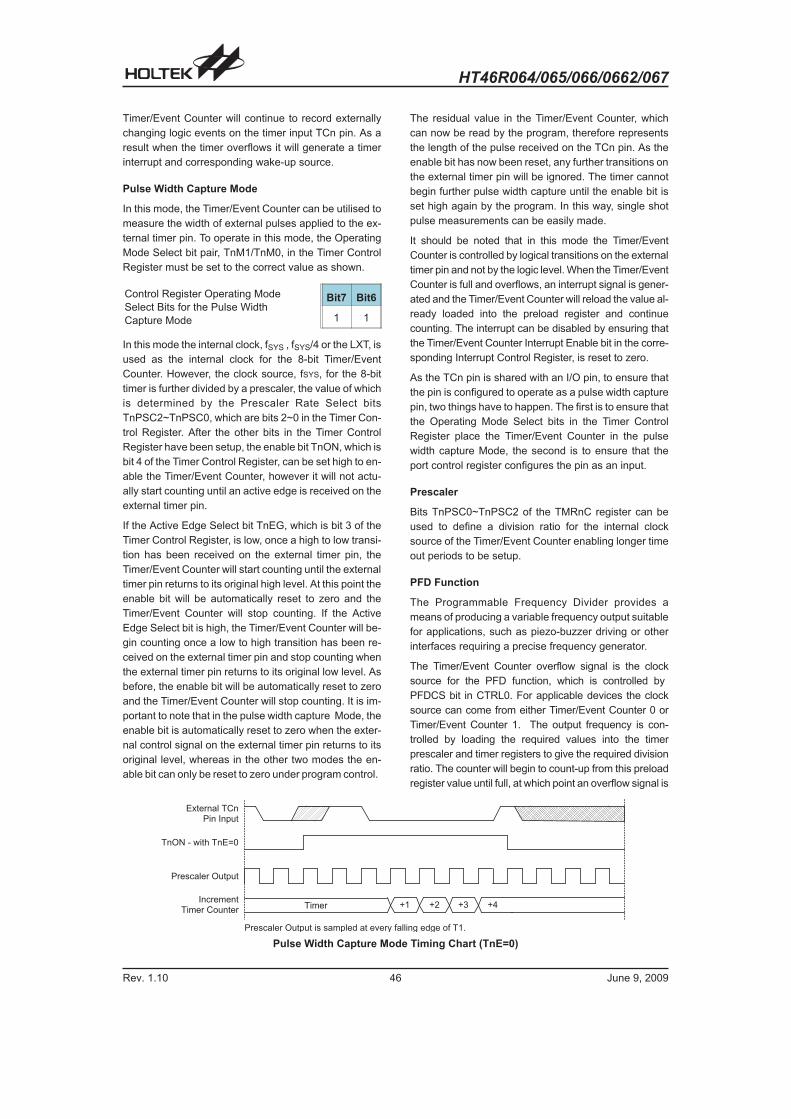
HT46R064/065/066/0662/067
Rev. 1.10 46 June 9, 2009
Timer/Event Counter will continue to record externally
changing logic events on the timer input TCn pin. As a
result when the timer overflows it will generate a timer
interrupt and corresponding wake-up source.
Pulse Width Capture Mode
In this mode, the Timer/Event Counter can be utilised to
measure the width of external pulses applied to the ex-
ternal timer pin. To operate in this mode, the Operating
Mode Select bit pair, TnM1/TnM0, in the Timer Control
Register must be set to the correct value as shown.
Control Register Operating Mode
Select Bits for the Pulse Width
Capture Mode
Bit7 Bit6
1 1
In this mode the internal clock, fSYS , fSYS/4 or the LXT, is
used as the internal clock for the 8-bit Timer/Event
Counter. However, the clock source, fSYS, for the 8-bit
timer is further divided by a prescaler, the value of which
is determined by the Prescaler Rate Select bits
TnPSC2~TnPSC0, which are bits 2~0 in the Timer Con-
trol Register. After the other bits in the Timer Control
Register have been setup, the enable bit TnON, which is
bit 4 of the Timer Control Register, can be set high to en-
able the Timer/Event Counter, however it will not actu-
ally start counting until an active edge is received on the
external timer pin.
If the Active Edge Select bit TnEG, which is bit 3 of the
Timer Control Register, is low, once a high to low transi-
tion has been received on the external timer pin, the
Timer/Event Counter will start counting until the external
timer pin returns to its original high level. At this point the
enable bit will be automatically reset to zero and the
Timer/Event Counter will stop counting. If the Active
Edge Select bit is high, the Timer/Event Counter will be-
gin counting once a low to high transition has been re-
ceived on the external timer pin and stop counting when
the external timer pin returns to its original low level. As
before, the enable bit will be automatically reset to zero
and the Timer/Event Counter will stop counting. It is im-
portant to note that in the pulse width capture Mode, the
enable bit is automatically reset to zero when the exter-
nal control signal on the external timer pin returns to its
original level, whereas in the other two modes the en-
able bit can only be reset to zero under program control.
The residual value in the Timer/Event Counter, which
can now be read by the program, therefore represents
the length of the pulse received on the TCn pin. As the
enable bit has now been reset, any further transitions on
the external timer pin will be ignored. The timer cannot
begin further pulse width capture until the enable bit is
set high again by the program. In this way, single shot
pulse measurements can be easily made.
It should be noted that in this mode the Timer/Event
Counter is controlled by logical transitions on the external
timer pin and not by the logic level. When the Timer/Event
Counter is full and overflows, an interrupt signal is gener-
ated and the Timer/Event Counter will reload the value al-
ready loaded into the preload register and continue
counting. The interrupt can be disabled by ensuring that
the Timer/Event Counter Interrupt Enable bit in the corre-
sponding Interrupt Control Register, is reset to zero.
As the TCn pin is shared with an I/O pin, to ensure that
the pin is configured to operate as a pulse width capture
pin, two things have to happen. The first is to ensure that
the Operating Mode Select bits in the Timer Control
Register place the Timer/Event Counter in the pulse
width capture Mode, the second is to ensure that the
port control register configures the pin as an input.
Prescaler
Bits TnPSC0~TnPSC2 of the TMRnC register can be
used to define a division ratio for the internal clock
source of the Timer/Event Counter enabling longer time
out periods to be setup.
PFD Function
The Programmable Frequency Divider provides a
means of producing a variable frequency output suitable
for applications, such as piezo-buzzer driving or other
interfaces requiring a precise frequency generator.
The Timer/Event Counter overflow signal is the clock
source for the PFD function, which is controlled by
PFDCS bit in CTRL0. For applicable devices the clock
source can come from either Timer/Event Counter 0 or
Timer/Event Counter 1. The output frequency is con-
trolled by loading the required values into the timer
prescaler and timer registers to give the required division
ratio. The counter will begin to count-up from this preload
register value until full, at which point an overflow signal is
9 ( 9 & 9 , 9 #� � � � �
* 7 � � � � : � � � � � � < 8 �
� � . � � � C � � 3 � � * K $
� � � � 2 � : � � � � 8 � < 8 �
� 2 � � � � �� � � � � � 8 � � �
� � � � 2 � : � � � � 8 � < 8 � � � � � � � � < : � B � � � � � � � � � � A � : : � ! � � B ! � � A � � ( 4
Pulse Width Capture Mode Timing Chart (TnE=0)
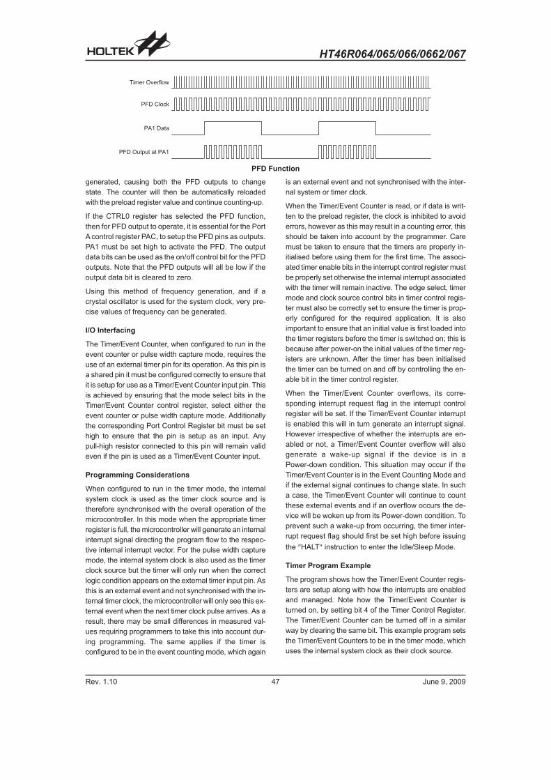
HT46R064/065/066/0662/067
Rev. 1.10 47 June 9, 2009
generated, causing both the PFD outputs to change
state. The counter will then be automatically reloaded
with the preload register value and continue counting-up.
If the CTRL0 register has selected the PFD function,
then for PFD output to operate, it is essential for the Port
A control register PAC, to setup the PFD pins as outputs.
PA1 must be set high to activate the PFD. The output
data bits can be used as the on/off control bit for the PFD
outputs. Note that the PFD outputs will all be low if the
output data bit is cleared to zero.
Using this method of frequency generation, and if a
crystal oscillator is used for the system clock, very pre-
cise values of frequency can be generated.
I/O Interfacing
The Timer/Event Counter, when configured to run in the
event counter or pulse width capture mode, requires the
use of an external timer pin for its operation. As this pin is
a shared pin it must be configured correctly to ensure that
it is setup for use as a Timer/Event Counter input pin. This
is achieved by ensuring that the mode select bits in the
Timer/Event Counter control register, select either the
event counter or pulse width capture mode. Additionally
the corresponding Port Control Register bit must be set
high to ensure that the pin is setup as an input. Any
pull-high resistor connected to this pin will remain valid
even if the pin is used as a Timer/Event Counter input.
Programming Considerations
When configured to run in the timer mode, the internal
system clock is used as the timer clock source and is
therefore synchronised with the overall operation of the
microcontroller. In this mode when the appropriate timer
register is full, the microcontroller will generate an internal
interrupt signal directing the program flow to the respec-
tive internal interrupt vector. For the pulse width capture
mode, the internal system clock is also used as the timer
clock source but the timer will only run when the correct
logic condition appears on the external timer input pin. As
this is an external event and not synchronised with the in-
ternal timer clock, the microcontroller will only see this ex-
ternal event when the next timer clock pulse arrives. As a
result, there may be small differences in measured val-
ues requiring programmers to take this into account dur-
ing programming. The same applies if the timer is
configured to be in the event counting mode, which again
is an external event and not synchronised with the inter-
nal system or timer clock.
When the Timer/Event Counter is read, or if data is writ-
ten to the preload register, the clock is inhibited to avoid
errors, however as this may result in a counting error, this
should be taken into account by the programmer. Care
must be taken to ensure that the timers are properly in-
itialised before using them for the first time. The associ-
ated timer enable bits in the interrupt control register must
be properly set otherwise the internal interrupt associated
with the timer will remain inactive. The edge select, timer
mode and clock source control bits in timer control regis-
ter must also be correctly set to ensure the timer is prop-
erly configured for the required application. It is also
important to ensure that an initial value is first loaded into
the timer registers before the timer is switched on; this is
because after power-on the initial values of the timer reg-
isters are unknown. After the timer has been initialised
the timer can be turned on and off by controlling the en-
able bit in the timer control register.
When the Timer/Event Counter overflows, its corre-
sponding interrupt request flag in the interrupt control
register will be set. If the Timer/Event Counter interrupt
is enabled this will in turn generate an interrupt signal.
However irrespective of whether the interrupts are en-
abled or not, a Timer/Event Counter overflow will also
generate a wake-up signal if the device is in a
Power-down condition. This situation may occur if the
Timer/Event Counter is in the Event Counting Mode and
if the external signal continues to change state. In such
a case, the Timer/Event Counter will continue to count
these external events and if an overflow occurs the de-
vice will be woken up from its Power-down condition. To
prevent such a wake-up from occurring, the timer inter-
rupt request flag should first be set high before issuing
the �HALT� instruction to enter the Idle/Sleep Mode.
Timer Program Example
The program shows how the Timer/Event Counter regis-
ters are setup along with how the interrupts are enabled
and managed. Note how the Timer/Event Counter is
turned on, by setting bit 4 of the Timer Control Register.
The Timer/Event Counter can be turned off in a similar
way by clearing the same bit. This example program sets
the Timer/Event Counters to be in the timer mode, which
uses the internal system clock as their clock source.
� � � � � � � � � � A : C
� � � � : 2 ;
� � ( � � � � �
� � � � � 8 � < 8 � � � � � � � (
PFD Function

HT46R064/065/066/0662/067
Rev. 1.10 48 June 9, 2009
� PFD Programming Example
org 04h ; external interrupt vector
org 08h ; Timer Counter 0 interrupt vectorjmp tmr0int ; jump here when Timer 0 overflows: :org 20h ; main program: :;internal Timer 0 interrupt routinetmr0int::; Timer 0 main program placed here:
:begin:;setup Timer 0 registersmov a,09bh ; setup Timer 0 preload valuemov tmr0,amov a,081h ; setup Timer 0 control registermov tmr0c,a ; timer mode and prescaler set to /2;setup interrupt registermov a,00dh ; enable master interrupt and both timer interruptsmov intc0,a: :set tmr0c.4 ; start Timer 0: :
Time Base
The device includes a Time Base function which is used to generate a regular time interval signal.
The Time Base time interval magnitude is determined using an internal 13 stage counter sets the division ratio of the
clock source. This division ratio is controlled by both the TBSEL0 and TBSEL1 bits in the CTRL1 register. The clock
source is selected using the T0S bit in the TMR0C register.
When the Time Base time out, a Time Base interrupt signal will be generated. It should be noted that as the Time Base
clock source is the same as the Timer/Event Counter clock source, care should be taken when programming.

HT46R064/065/066/0662/067
Rev. 1.10 49 June 9, 2009
Pulse Width Modulator
Every device includes a multiple output 8-bit PWM
function. Useful for such applications such as motor
speed control, the PWM function provides outputs with a
fixed frequency but with a duty cycle that can be varied
by setting particular values into the corresponding PWM
register.
Device Channels Mode Pins Registers
HT46R064
HT46R0651
6+2
7+1
PA4 PWM0
HT46R066
HT46R06622
PA4
PC3
PWM0
PWM1
HT46R067 3
PA4
PC3
PC2
PWM0
PWM1
PWM2
PWM Operation
A single register, known as PWMn and located in the
Data Memory is assigned to each Pulse Width Modula-
tor channel. It is here that the 8-bit value, which repre-
sents the overall duty cycle of one modulation cycle of
the output waveform, should be placed. To increase the
PWM modulation frequency, each modulation cycle is
subdivided into two or four individual modulation sub-
sections, known as the 7+1 mode or 6+2 mode respec-
tively. The required mode and the on/off control for each
PWM channel is selected using the CTRL0 and CTRL2
registers. Note that when using the PWM, it is only nec-
essary to write the required value into the PWMn regis-
ter and select the required mode setup and on/off
control using the CTRL0 and CTRL2 registers, the sub-
division of the waveform into its sub-modulation cycles
is implemented automatically within the microcontroller
hardware. The PWM clock source is the system clock
fSYS. This method of dividing the original modulation cy-
cle into a further 2 or 4 sub-cycles enable the generation
of higher PWM frequencies which allow a wider range of
applications to be served. The difference between what
is known as the PWM cycle frequency and the PWM
modulation frequency should be understood. As the
PWM clock is the system clock, fSYS, and as the PWM
value is 8-bits wide, the overall PWM cycle frequency is
fSYS/256. However, when in the 7+1 mode of operation
the PWM modulation frequency will be fSYS/128, while
the PWM modulation frequency for the 6+2 mode of op-
eration will be fSYS/64.
PWM
Modulation
PWM Cycle
Frequency
PWM Cycle
Duty
fSYS/64 for (6+2) bits mode
fSYS/128for (7+1) bits modefSYS/256 [PWM]/256
6+2 PWM Mode
Each full PWM cycle, as it is controlled by an 8-bit PWM
register, has 256 clock periods. However, in the 6+2
PWM mode, each PWM cycle is subdivided into four in-
dividual sub-cycles known as modulation cycle 0 ~ mod-
ulation cycle 3, denoted as i in the table. Each one of
these four sub-cycles contains 64 clock cycles. In this
mode, a modulation frequency increase of four is
achieved. The 8-bit PWM register value, which repre-
sents the overall duty cycle of the PWM waveform, is di-
vided into two groups. The first group which consists of
bit2~bit7 is denoted here as the DC value. The second
group which consists of bit0~bit1 is known as the AC
value. In the 6+2 PWM mode, the duty cycle value of
each of the four modulation sub-cycles is shown in the
following table.
Parameter AC (0~3)DC
(Duty Cycle)
Modulation cycle i
(i=0~3)
i<ACDC+1
64
i�ACDC
64
6+2 Mode Modulation Cycle Values
The following diagram illustrates the waveforms associ-
ated with the 6+2 mode of PWM operation. It is impor-
tant to note how the single PWM cycle is subdivided into
4 individual modulation cycles, numbered from 0~3 and
how the AC value is related to the PWM value.
� � � $ � � 8 � � � � � ! � � � � �
� � � � � � � < � � � � � � $
� � � ( � � 8 � � � � � ! � � � � �
� � � & � � � � ! � � � � �
� � � � � � � < � � � � � � (
� � � � � � � < � � � � � � &
� � � � � � 5 ) 9 ( 6 � 5 ' 9 & 6� � � � 8 � � �
� � � $
� � � (
� � � &
PWM Block Diagram

HT46R064/065/066/0662/067
Rev. 1.10 50 June 9, 2009
7+1 PWM Mode
Each full PWM cycle, as it is controlled by an 8-bit PWM
register, has 256 clock periods. However, in the 7+1
PWM mode, each PWM cycle is subdivided into two indi-
vidual sub-cycles known as modulation cycle 0 ~ modula-
tion cycle 1, denoted as i in the table. Each one of these
two sub-cycles contains 128 clock cycles. In this mode, a
modulation frequency increase of two is achieved. The
8-bit PWM register value, which represents the overall
duty cycle of the PWM waveform, is divided into two
groups. The first group which consists of bit1~bit7 is de-
noted here as the DC value. The second group which
consists of bit0 is known as the AC value. In the 7+1
PWM mode, the duty cycle value of each of the two mod-
ulation sub-cycles is shown in the following table.
Parameter AC (0~1)DC
(Duty Cycle)
Modulation cycle i
(i=0~1)
i<ACDC+1
128
i�ACDC
128
7+1 Mode Modulation Cycle Values
The following diagram illustrates the waveforms associ-
ated with the 7+1 mode PWM operation. It is important
to note how the single PWM cycle is subdivided into 2 in-
dividual modulation cycles, numbered 0 and 1 and how
the AC value is related to the PWM value.
PWM Output Control
The PWM outputs are pin-shared with the I/O pins PA4,
PC2 and PC3. To operate as a PWM output and not as
an I/O pin, the correct bits must be set in the CTRL0 and
CTRL2 register. A zero value must also be written to the
corresponding bit in the I/O port control register PAC.4,
PCC.2 and PCC.3 to ensure that the corresponding
PWM output pin is setup as an output. After these two
initial steps have been carried out, and of course after
the required PWM value has been written into the
PWMn register, writing a high value to the correspond-
ing bit in the output data register PA.4, PC.2 and PC.3
will enable the PWM data to appear on the pin. Writing a
zero value will disable the PWM output function and
force the output low. In this way, the Port data output
registers can be used as an on/off control for the PWM
function. Note that if the CTRL0 and CTRL2 registers
have selected the PWM function, but a high value has
been written to its corresponding bit in the PAC or PCC
control register to configure the pin as an input, then the
pin can still function as a normal input line, with pull-high
resistor options.
A = � &
� � �
/ � � � 0 � K ( $ $
/ � � � 0 � K ( $ (
� � �
/ � � � 0 � K ( $ &
� � �
/ � � � 0 � K ( $ ,
� � �
� � � � 2 � 2 : � � > � & % ' � A =
& % � ' #
& ' � ' #
& ' � ' #
& ' � ' #
& % � ' # & % � ' # & % � ' #
& % � ' #
& % � ' #
& % � ' #
& % � ' #
& ' � ' #
& ' � ' #
& % � ' #
& % � ' #
& ' � ' # & % � ' #
& ' � ' #
& ' � ' #
& ' � ' #
� B 8 : � � � � 2 � 2 : � � $
� � � � � B 8 : � � � � < � � � B � > � ' # � A =
� B 8 : � � � � 2 � 2 : � � ( � B 8 : � � � � 2 � 2 : � � & � B 8 : � � � � 2 � 2 : � � , � B 8 : � � � � 2 � 2 : � � $
6+2 PWM Mode
� * � � � ' % # � + � , � - � � .
� ) � $
� � � � � : 8 �
� � � � : 8 �
PWM Register for 6+2 Mode

HT46R064/065/066/0662/067
Rev. 1.10 51 June 9, 2009
� PWM Programming Example
The following sample program shows how the PWM0 output is setup and controlled.mov a,64h ; setup PWM value of decimal 100mov pwm0,aset ctrl0.5 ; select the 7+1 PWM modeset ctrl0.3 ; select pin PA4 to have a PWM functionclr pac.4 ; setup pin PA4 as an outputset pa.4 ; enable the PWM output: :clr pa.4 ; disable the PWM output_ pin
; PA4 forced low
A = � &
� � �
/ � � � 0 � K ( $ $
/ � � � 0 � K ( $ (
� � �
/ � � � 0 � K ( $ &
� � �
/ � � � 0 � K ( $ ,
� � �
� � � � � B 8 : � � � � < � � � B � > � ( & � � A =
% $ � ( & �
% ( � ( & �
% ( � ( & �
% & � ( & �
% $ � ( & �
% $ � ( & �
% ( � ( & �
% ( � ( & �
% $ � ( & �
% ( � ( & �
% ( � ( & �
% & � ( & �
� B 8 : � � � � 2 � 2 : � � $
� � � � 2 � 2 : � � > � & % ' � A =
� B 8 : � � � � 2 � 2 : � � ( � B 8 : � � � � 2 � 2 : � � $
7+1 PWM Mode
� * � � � ' % # � + � , � - � � .
� ) � $
� � � � � : 8 �
� � � � : 8 �
PWM Register for 7+1 Mode

HT46R064/065/066/0662/067
Rev. 1.10 52 June 9, 2009
Analog to Digital Converter
The need to interface to real world analog signals is a
common requirement for many electronic systems.
However, to properly process these signals by a
microcontroller, they must first be converted into digital
signals by A/D converters. By integrating the A/D con-
version electronic circuitry into the microcontroller, the
need for external components is reduced significantly
with the corresponding follow-on benefits of lower costs
and reduced component space requirements.
A/D Overview
The device contains an 4/8-channel analog to digital
converter which can directly interface to external analog
signals, such as that from sensors or other control sig-
nals and convert these signals directly into either a
12-bit digital value.
Part No.Input
Channels
Conversion
Bits
Input
Pins
HT46R064
HT46R0654 12 PA0~PA3
Other
Devices8 12
PA0~PA3
PC0~PC1
PC6~PC7
The accompanying block diagram shows the overall in-
ternal structure of the A/D converter, together with its as-
sociated registers.
A/D Converter Data Registers � ADRL, ADRH
The device, which has an internal 12-bit A/D converter,
requires two data registers, a high byte register, known
as ADRH, and a low byte register, known as ADRL. After
the conversion process takes place, these registers can
be directly read by the microcontroller to obtain the digit-
ised conversion value. Only the high byte register,
ADRH, utilises its full 8-bit contents. The low byte regis-
ter utilises only 4 bit of its 8-bit contents as it contains
only the lowest bits of the 12-bit converted value.
In the following table, D0~D11 is the A/D conversion
data result bits.
RegisterBit
7
Bit
6
Bit
5
Bit
4
Bit
3
Bit
2
Bit
1
Bit
0
ADRL D3 D2 D1 D0 � � � �
ADRH D11 D10 D9 D8 D7 D6 D5 D4
A/D Data Registers
A/D Converter Control Registers � ADCR, ACSR
To control the function and operation of the A/D con-
verter, two control registers known as ADCR and ACSR
are provided. These 8-bit registers define functions
such as the selection of which analog channel is con-
nected to the internal A/D converter, which pins are
used as analog inputs and which are used as normal
I/Os, the A/D clock source as well as controlling the start
function and monitoring the A/D converter end of con-
version status.
The ACS2~ACS0 bits in the ADCR register define the
channel number. As the device contains only one actual
analog to digital converter circuit, each of the individual
8 analog inputs must be routed to the converter. It is the
function of the ACS2~ACS0 bits in the ADCR register to
determine which analog channel is actually connected
to the internal A/D converter.
The ADCR control register also contains the
PCR2~PCR0 bits which determine which pins on
PA0~PA3, PC0, PC1, PC6, PC7 are used as analog in-
puts for the A/D converter and which pins are to be used
as normal I/O pins. If the 3-bit address on PCR2~PCR0
has a value of �111�, then all eight pins, namely
AN0~AN7 will all be set as analog inputs. Note that if the
PCR2~PCR0 bits are all set to zero, then all the
PA0~PA3, PC0, PC1, PC6, PC7 pins will be setup as nor-
mal I/Os.
�
: 2 ;� � � � B � �� � .
� � � � � ! � � � � �
� � � � � �
� � � @
� � � � � � � �� � ! � � � � � �
� � $ D � � & � � $ D � � & � � � � * � �� � �� � ! � � � � �
� � � . � � � � �� � � � * � � : �
A =
� � $ � � . $� � ( � � . (� � & � � . &� � , � � . ,� $ � � . #� ( � � . %� ' � � . '� ) � � . )
A/D Converter Structure
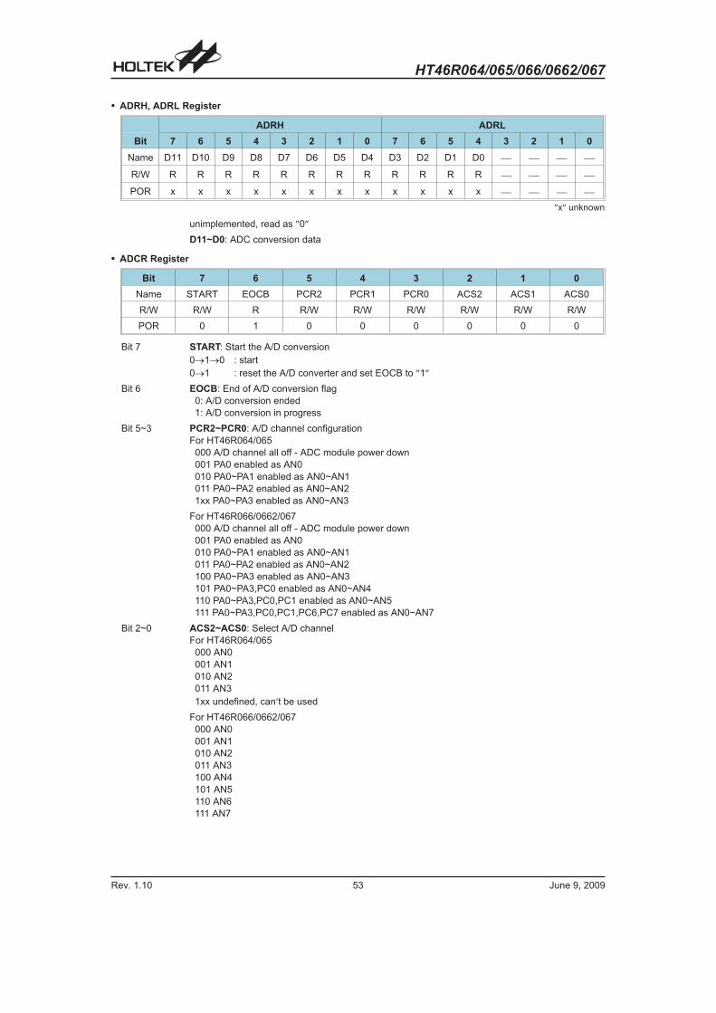
HT46R064/065/066/0662/067
Rev. 1.10 53 June 9, 2009
� ADRH, ADRL Register
ADRH ADRL
Bit 7 6 5 4 3 2 1 0 7 6 5 4 3 2 1 0
Name D11 D10 D9 D8 D7 D6 D5 D4 D3 D2 D1 D0 � � � �
R/W R R R R R R R R R R R R � � � �
POR x x x x x x x x x x x x � � � �
�x� unknown
unimplemented, read as �0�
D11~D0: ADC conversion data
� ADCR Register
Bit 7 6 5 4 3 2 1 0
Name START EOCB PCR2 PCR1 PCR0 ACS2 ACS1 ACS0
R/W R/W R R/W R/W R/W R/W R/W R/W
POR 0 1 0 0 0 0 0 0
Bit 7 START: Start the A/D conversion
0�1�0 : start
0�1 : reset the A/D converter and set EOCB to �1�
Bit 6 EOCB: End of A/D conversion flag
0: A/D conversion ended
1: A/D conversion in progress
Bit 5~3 PCR2~PCR0: A/D channel configuration
For HT46R064/065
000 A/D channel all off - ADC module power down
001 PA0 enabled as AN0
010 PA0~PA1 enabled as AN0~AN1
011 PA0~PA2 enabled as AN0~AN2
1xx PA0~PA3 enabled as AN0~AN3
For HT46R066/0662/067
000 A/D channel all off - ADC module power down
001 PA0 enabled as AN0
010 PA0~PA1 enabled as AN0~AN1
011 PA0~PA2 enabled as AN0~AN2
100 PA0~PA3 enabled as AN0~AN3
101 PA0~PA3,PC0 enabled as AN0~AN4
110 PA0~PA3,PC0,PC1 enabled as AN0~AN5
111 PA0~PA3,PC0,PC1,PC6,PC7 enabled as AN0~AN7
Bit 2~0 ACS2~ACS0: Select A/D channel
For HT46R064/065
000 AN0
001 AN1
010 AN2
011 AN3
1xx undefined, cant be used
For HT46R066/0662/067
000 AN0
001 AN1
010 AN2
011 AN3
100 AN4
101 AN5
110 AN6
111 AN7

HT46R064/065/066/0662/067
Rev. 1.10 54 June 9, 2009
The START bit in the register is used to start and reset
the A/D converter. When themicrocontroller sets this bit
from low to high and then low again, an analog to digital
conversion cycle will be initiated. When the START bit is
brought from low to high but not low again, the EOCB bit
in the ADCR register will be set to a �1� and the analog
to digital converter will be reset. It is the START bit that is
used to control the overall start operation of the internal
analog to digital converter.
The EOCB bit in the ADCR register is used to indicate
when the analog to digital conversion process is com-
plete. This bit will be automatically set to �0� by the
microcontroller after a conversion cycle has ended. In
addition, the corresponding A/D interrupt request flag
will be set in the interrupt control register, and if the inter-
rupts are enabled, an appropriate internal interrupt sig-
nal will be generated. This A/D internal interrupt signal
will direct the program flow to the associated A/D inter-
nal interrupt address for processing. If the A/D internal
interrupt is disabled, the microcontroller can be used to
poll the EOCB bit in the ADCR register to check whether
it has been cleared as an alternative method of detect-
ing the end of an A/D conversion cycle.
The clock source for the A/D converter, which originates
from the system clock fSYS, is first divided by a division
ratio, the value of which is determined by the ADCS2,
ADCS1 and ADCS0 bits in the ACSR register.
Controlling the power on/off function of the A/D con-
verter circuitry is implemented using the value of the
ADONB bit.
Although the A/D clock source is determined by the sys-
tem clock fSYS, and by bits ADCS2, ADCS1 and ADCS0,
there are some limitations on the maximum A/D clock
source speed that can be selected. As the minimum value
of permissible A/D clock period, tAD, is 0.5�s, care must be
taken for system clock speeds in excess of 4MHz. For
system clock speeds in excess of 4MHz, the ADCS2,
ADCS1 and ADCS0 bits should not be set to �000�. Doing
so will give A/D clock periods that are less than the mini-
mum A/D clock period which may result in inaccurate A/D
conversion values. Refer to the following table for exam-
ples, where values marked with an asterisk * show where,
depending upon the device, special care must be taken,
as the values may be less than the specified minimum A/D
Clock Period.
� ACSR Register
Bit 7 6 5 4 3 2 1 0
Name TEST ADONB � � � ADCS2 ADCS1 ADCS0
R/W R/W R/W � � � R/W R/W R/W
POR 1 0 � � � 0 0 0
Bit 7 TEST: for test mode use only
Bit 6 ADONB: ADC module power on/off control bit
0: ADC module power on
1: ADC module power off
Note: 1. it is recommended to set ADONB=1 before entering idle/sleep for saving power.
2. ADONB=1 will power down the ADC module.
Bit 5~3 unimplemented, read as �0�
Bit 2~0 ADCS2~ADCS0: Select A/D converter clock source
000: system clock/2
001: system clock/8
010: system clock/32
011: undefined, cant be used.
100: system clock
101: system clock/4
110: system clock/16
111: undefined, cant be used.

HT46R064/065/066/0662/067
Rev. 1.10 55 June 9, 2009
fSYS
A/D Clock Period (tAD)
ADCS2,
ADCS1,
ADCS0=000
(fSYS/2)
ADCS2,
ADCS1,
ADCS0=001
(fSYS/8)
ADCS2,
ADCS1,
ADCS0=010
(fSYS/32)
ADCS2,
ADCS1,
ADCS0=100
(fSYS)
ADCS2,
ADCS1,
ADCS0=101
(fSYS/4)
ADCS2,
ADCS1,
ADCS0=110
(fSYS/16)
ADCS2,
ADCS1,
ADCS0=011,
111
1MHz 2�s 8�s 32�s 1�s 4�s 16�s Undefined
2MHz 1�s 4�s 16�s 500ns 2�s 8�s Undefined
4MHz 500ns 2�s 8�s 250ns* 1�s 4�s Undefined
8MHz 250ns* 1�s 4�s 125ns* 500ns 2�s Undefined
12MHz 167ns* 667ns 2.67�s 83ns* 333ns* 1�s Undefined
A/D Clock Period Examples
A/D Input Pins
All of the A/D analog input pins are pin-shared with the
I/O pins on Port A. Bits PCR2~PCR0 in the register, de-
termine whether the input pins are setup as normal Port
A input/output pins or whether they are setup as analog
inputs. In this way, pins can be changed under program
control to change their function from normal I/O opera-
tion to analog inputs and vice versa. Pull-high resistors,
which are setup through register programming, apply to
the input pins only when they are used as normal I/O
pins, if setup as A/D inputs the pull-high resistors will be
automatically disconnected. Note that it is not neces-
sary to first setup the A/D pin as an input in the PBC port
control register to enable the A/D input as when the
PCR2~PCR0 bits enable an A/D input, the status of the
port control register will be overridden.
Summary of A/D Conversion Steps
The following summarises the individual steps that
should be executed in order to implement an A/D con-
version process.
� Step 1
Select the required A/D conversion clock by correctly
programming bits ADCS2, ADCS1 and ADCS0 in the
register.
� Step 2
Select which pins are to be used as A/D inputs and
configure them as A/D input pins by correctly pro-
gramming the PCR2~PCR0 bits in the ADCR register.
� Step 3
Enable the A/D by clearing the ADONB in the ACSR
register to zero.
� Step 4
Select which channel is to be connected to the internal
A/D converter by correctly programming the
ACS2~ACS0 bits which are also contained in the reg-
ister.
� Step 5
If the interrupts are to be used, the interrupt control reg-
isters must be correctly configured to ensure the A/D
converter interrupt function is active. The master inter-
rupt control bit, EMI, the INTC0 interrupt control regis-
ter must be set to �1�, the A/D converter interrupt bit,
ADE, must also be set to �1�.
� Step 6
The analog to digital conversion process can now be
initialised by setting the START bit in the ADCR regis-
ter from �0� to �1� and then to �0� again. Note that this
bit should have been originally set to �0�.
� Step 7
To check when the analog to digital conversion pro-
cess is complete, the EOCB bit in the ADCR register
can be polled. The conversion process is complete
when this bit goes low. When this occurs the A/D data
registers ADRL and ADRH can be read to obtain the
conversion value. As an alternative method if the in-
terrupts are enabled and the stack is not full, the pro-
gram can wait for an A/D interrupt to occur.
Note: When checking for the end of the conversion
process, if the method of polling the EOCB bit in
the ADCR register is used, the interrupt enable
step above can be omitted.
The accompanying diagram shows graphically the vari-
ous stages involved in an analog to digital conversion
process and its associated timing.
The setting up and operation of the A/D converter func-
tion is fully under the control of the application program as
there are no configuration options associated with the
A/D converter. After an A/D conversion process has been
initiated by the application program, the microcontroller
internal hardware will begin to carry out the conversion,
during which time the program can continue with other
functions. The time taken for the A/D conversion is 16tAD
where tAD is equal to the A/D clock period.

HT46R064/065/066/0662/067
Rev. 1.10 56 June 9, 2009
Programming Considerations
When programming, special attention must be given to
the PCR[2:0] bits in the register. If these bits are all
cleared to zero no external pins will be selected for use
as A/D input pins allowing the pins to be used as normal
I/O pins. When this happens the internal A/D circuitry
will be power down. Setting the ADONB bit high has the
ability to power down the internal A/D circuitry, which
may be an important consideration in power sensitive
applications.
A/D Transfer Function
As the device contain a 12-bit A/D converter, its
full-scale converted digitised value is equal to FFFH.
Since the full-scale analog input value is equal to the
VDD voltage, this gives a single bit analog input value of
VDD/4096. The diagram show the ideal transfer function
between the analog input value and the digitised output
value for the A/D converter.
Note that to reduce the quantisation error, a 0.5 LSB off-
set is added to the A/D Converter input. Except for the
digitised zero value, the subsequent digitised values will
change at a point 0.5 LSB below where they would
change without the offset, and the last full scale digitised
value will change at a point 1.5 LSB below the VDD level.
A/D Programming Example
The following two programming examples illustrate how
to setup and implement an A/D conversion. In the first
example, the method of polling the EOCB bit in the
ADCR register is used to detect when the conversion
cycle is complete, whereas in the second example, the
A/D interrupt is used to determine when the conversion
is complete.
� � �
� � � � 2 � � � � � � � � � �
$ $ $ �
7 7 7 �
7 7 7 � � � � � � / & > $ 0 � � � � � � � G 8 � : � � � E $ E
$ ( $ �
� � � �
* � �
� � & D� � $
� & D� $
� C � � � � � � � �
* B � A � � � �2 � � � � � ( > � � � A � � � < � � � 2 A � ! 8 � � � �
& > � � : � 2 � � � � : ! � 2 3 � � :
� � � � 2 : 2 ; � � 8 � � � � � � A � � � ? � A = � & ? � A = � # ? � A = � � ? � A = � ( ' � � � A = � , &� � � K # � � �
� � � K � ( ' � � �
. � � > �
� � � � � A � � � �2 � � � � �
� � � � � � � � �2 � � � � � �
� � � � � � � < : � ! � � � � �� � � � � �
$ $ $ �
� � � � � A � � � �2 � � � � �
� � � � � � � � �2 � � � � � �
$ $ ( �
� � � � � A � � � �2 � � � � �
� � � � � � � � �2 � � � � � �
* B � A � � � �2 � � � � �
� � � � � � � < : � ! � � � � �� � � � � �
� � � � B 8 : �� .
� � � . �
A A
� � . & �
� � �
� � � � 2 � � � � � � � � � �
A/D Conversion Timing
� � * @
5 � � � � � � � � � 6
� � � � � � � � � � � � 8 : �
� � � @
� � � @
$ , @
$ & @
$ ( @
$ 4 % � � �
$ ( & , # $ - , # $ - # # $ - % # $ - '
� � : ! � � < 8 � � + : � � ! �
( 4 % � � �
+ � �
# $ - '
Ideal A/D Transfer Function
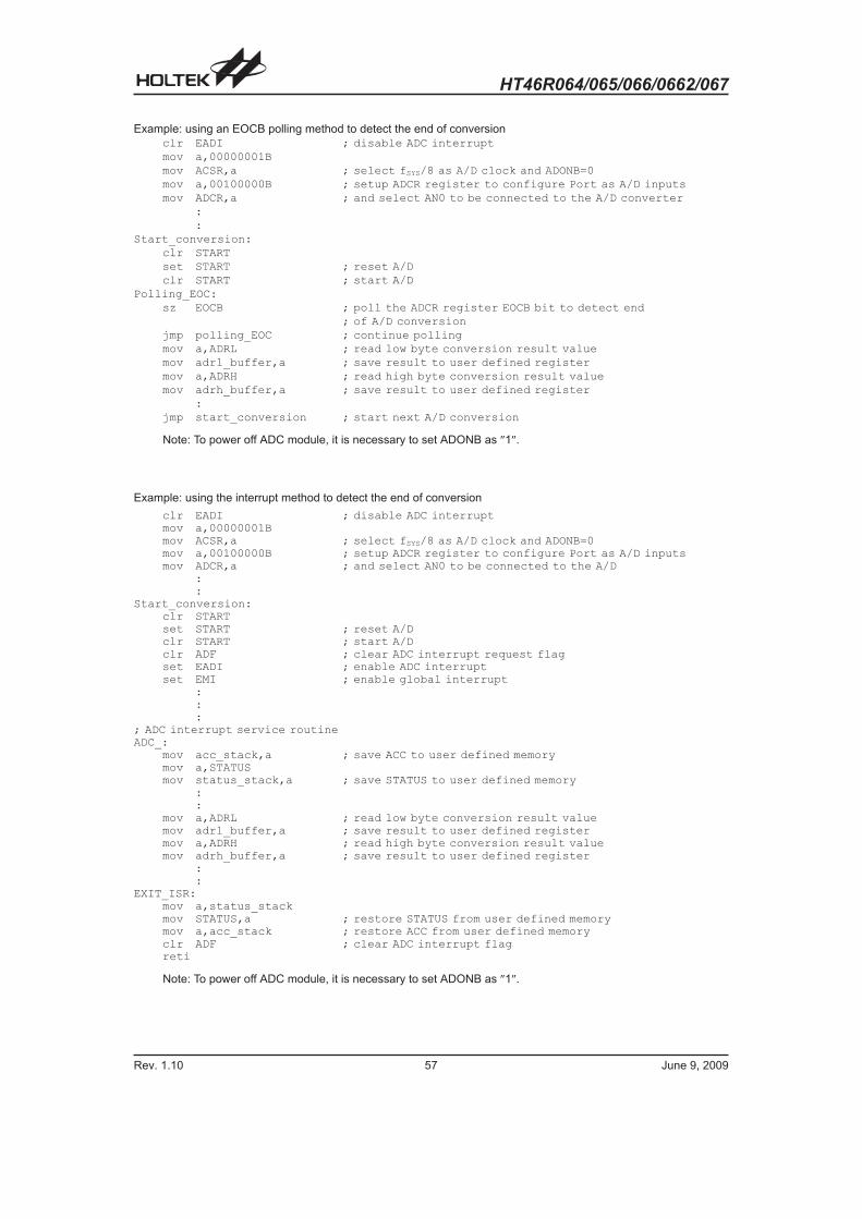
HT46R064/065/066/0662/067
Rev. 1.10 57 June 9, 2009
Example: using an EOCB polling method to detect the end of conversion
clr EADI ; disable ADC interruptmov a,00000001Bmov ACSR,a ; select fSYS/8 as A/D clock and ADONB=0mov a,00100000B ; setup ADCR register to configure Port as A/D inputsmov ADCR,a ; and select AN0 to be connected to the A/D converter
::
Start_conversion:clr STARTset START ; reset A/Dclr START ; start A/D
Polling_EOC:sz EOCB ; poll the ADCR register EOCB bit to detect end
; of A/D conversionjmp polling_EOC ; continue pollingmov a,ADRL ; read low byte conversion result valuemov adrl_buffer,a ; save result to user defined registermov a,ADRH ; read high byte conversion result valuemov adrh_buffer,a ; save result to user defined register
:jmp start_conversion ; start next A/D conversion
Note: To power off ADC module, it is necessary to set ADONB as �1�.
Example: using the interrupt method to detect the end of conversion
clr EADI ; disable ADC interruptmov a,00000001Bmov ACSR,a ; select fSYS/8 as A/D clock and ADONB=0mov a,00100000B ; setup ADCR register to configure Port as A/D inputsmov ADCR,a ; and select AN0 to be connected to the A/D
::
Start_conversion:clr STARTset START ; reset A/Dclr START ; start A/Dclr ADF ; clear ADC interrupt request flagset EADI ; enable ADC interruptset EMI ; enable global interrupt
:::
; ADC interrupt service routineADC_:
mov acc_stack,a ; save ACC to user defined memorymov a,STATUSmov status_stack,a ; save STATUS to user defined memory
::
mov a,ADRL ; read low byte conversion result valuemov adrl_buffer,a ; save result to user defined registermov a,ADRH ; read high byte conversion result valuemov adrh_buffer,a ; save result to user defined register
::
EXIT_ISR:mov a,status_stackmov STATUS,a ; restore STATUS from user defined memorymov a,acc_stack ; restore ACC from user defined memoryclr ADF ; clear ADC interrupt flagreti
Note: To power off ADC module, it is necessary to set ADONB as �1�.

HT46R064/065/066/0662/067
Rev. 1.10 58 June 9, 2009
Interrupts
Interrupts are an important part of any microcontroller
system. When an external event or an internal function
such as a Timer/Event Counter or Time Base requires
microcontroller attention, their corresponding interrupt
will enforce a temporary suspension of the main pro-
gram allowing the microcontroller to direct attention to
their respective needs.
The devices contain a single external interrupt and mul-
tiple internal interrupts. The external interrupt is con-
trolled by the action of the external interrupt pin, while
the internal interrupt is controlled by the Timer/Event
Counters and Time Base overflows.
Interrupt Register
Overall interrupt control, which means interrupt enabling
and request flag setting, is controlled by using two regis-
ters, INTC0 and INTC1. By controlling the appropriate
enable bits in this registers each individual interrupt can
be enabled or disabled. Also when an interrupt occurs,
the corresponding request flag will be set by the
microcontroller. The global enable flag if cleared to zero
will disable all interrupts.
Interrupt Operation
A Timer/Event Counter overflow, a Time Base event or
an active edge on the external interrupt pin will all gener-
ate an interrupt request by setting their corresponding
request flag, if their appropriate interrupt enable bit is
set. When this happens, the Program Counter, which
stores the address of the next instruction to be exe-
cuted, will be transferred onto the stack. The Program
Counter will then be loaded with a new address which
will be the value of the corresponding interrupt vector.
The microcontroller will then fetch its next instruction
from this interrupt vector. The instruction at this vector
will usually be a JMP statement which will jump to an-
other section of program which is known as the interrupt
service routine. Here is located the code to control the
appropriate interrupt. The interrupt service routine must
be terminated with a RETI instruction, which retrieves
the original Program Counter address from the stack
and allows the microcontroller to continue with normal
execution at the point where the interrupt occurred.
The various interrupt enable bits, together with their as-
sociated request flags, are shown in the following dia-
gram with their order of priority.
Once an interrupt subroutine is serviced, all the other in-
terrupts will be blocked, as the EMI bit will be cleared au-
tomatically. This will prevent any further interrupt nesting
from occurring. However, if other interrupt requests oc-
cur during this interval, although the interrupt will not be
immediately serviced, the request flag will still be re-
corded. If an interrupt requires immediate servicing
while the program is already in another interrupt service
routine, the EMI bit should be set after entering the rou-
tine, to allow interrupt nesting. If the stack is full, the in-
terrupt request will not be acknowledged, even if the
related interrupt is enabled, until the Stack Pointer is
decremented. If immediate service is desired, the stack
must be prevented from becoming full.
� 8 � � � � � 2 � : : � � : � � � � B � � � � � �� � 8 � : : � � � � � � � : � � � � B � � � � A � C � � �
* 7 � � � � : � � � � � � 8 < �� � G 8 � � � � � : � ! � � . � �
� � � � � � * � � � � 8 � � � � $� � � � � 8 < � � � � G 8 � � � � � : � ! � � $ �
� . � *
� $ *
* � �
� � � � � � �
@ � ! 3
� C
� � � � � 8 < �� : : � !
� � *
* � �
� ( *
� & *
� � � � � � * � � � � 8 � � � � (� � � � � 8 < � � � � G 8 � � � � � : � ! � � ( �
� � � � � � * � � � � 8 � � � � &� � � � � 8 < � � � � G 8 � � � � � : � ! � � & �
� � � � � � � � � � � � � � 8 < � � � � G 8 � � � � � : � ! � � � �
� � *� � � � � � � � �� � � � � 8 < � � � � G 8 � � � � � : � ! � � � �
* � �
� 8 � � � � � 2 � : : � � � � � � � : � B � C 3 � � � � � � � 8 < �� � � � � � � � � � � � � 2 � B � * � � : � B � � � 8 � : : � � �� 8 � � � � � 2 � : : � � C � � 3 � � * � � � � � � � 8 2 � �
* � �
* � �
* � �
Interrupt Scheme
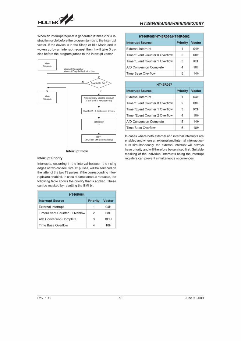
HT46R064/065/066/0662/067
Rev. 1.10 59 June 9, 2009
When an interrupt request is generated it takes 2 or 3 in-
struction cycle before the program jumps to the interrupt
vector. If the device is in the Sleep or Idle Mode and is
woken up by an interrupt request then it will take 3 cy-
cles before the program jumps to the interrupt vector.
Interrupt Priority
Interrupts, occurring in the interval between the rising
edges of two consecutive T2 pulses, will be serviced on
the latter of the two T2 pulses, if the corresponding inter-
rupts are enabled. In case of simultaneous requests, the
following table shows the priority that is applied. These
can be masked by resetting the EMI bit.
HT46R064
Interrupt Source Priority Vector
External Interrupt 1 04H
Timer/Event Counter 0 Overflow 2 08H
A/D Conversion Complete 3 0CH
Time Base Overflow 4 10H
HT46R065/HT46R066/HT46R0662
Interrupt Source Priority Vector
External Interrupt 1 04H
Timer/Event Counter 0 Overflow 2 08H
Timer/Event Counter 1 Overflow 3 0CH
A/D Conversion Complete 4 10H
Time Base Overflow 5 14H
HT46R067
Interrupt Source Priority Vector
External Interrupt 1 04H
Timer/Event Counter 0 Overflow 2 08H
Timer/Event Counter 1 Overflow 3 0CH
Timer/Event Counter 2 Overflow 4 10H
A/D Conversion Complete 5 14H
Time Base Overflow 6 18H
In cases where both external and internal interrupts are
enabled and where an external and internal interrupt oc-
curs simultaneously, the external interrupt will always
have priority and will therefore be serviced first. Suitable
masking of the individual interrupts using the interrupt
registers can prevent simultaneous occurrences.
Wait for 2 ~ 3 Instruction Cycles
Main
Program
ISR Entry
Enable Bit Set ?
Main
Program
RETI
(it will set EMI automatically)
Automatically Disable Interrupt
Clear EMI & Request Flag
Interrupt Request orInterrupt Flag Set by Instruction
Y
N
Interrupt Flow

HT46R064/065/066/0662/067
Rev. 1.10 60 June 9, 2009
External Interrupt
For an external interrupt to occur, the global interrupt en-
able bit, EMI, and external interrupt enable bit, INTE,
must first be set. An actual external interrupt will take
place when the external interrupt request flag, INTF, is
set, a situation that will occur when an edge transition
appears on the external INT line. The type of transition
that will trigger an external interrupt, whether high to low,
low to high or both is determined by the INTEG0 and
INTEG1 bits, which are bits 6 and 7 respectively, in the
CTRL1 control register. These two bits can also disable
the external interrupt function.
INTEG1 INTEG0 Edge Trigger Type
0 0 External interrupt disable
0 1 Rising edge Trigger
1 0 Falling edge Trigger
1 1 Both edge Trigger
The external interrupt pin is pin-shared with the I/O pin
PA3 and can only be configured as an external interrupt
pin if the corresponding external interrupt enable bit in
the INTC0 register has been set and the edge trigger
type has been selected using the CTRL1 register. The
pin must also be setup as an input by setting the corre-
sponding PAC.3 bit in the port control register. When the
interrupt is enabled, the stack is not full and a transition
appears on the external interrupt pin, a subroutine call to
the external interrupt vector at location 04H, will take
place. When the interrupt is serviced, the external inter-
rupt request flag, INTF, will be automatically reset and
the EMI bit will be automatically cleared to disable other
interrupts. Note that any pull-high resistor connections
on this pin will remain valid even if the pin is used as an
external interrupt input.
� HT46R064
� INTC0 Register
Bit 7 6 5 4 3 2 1 0
Name � ADF T0F INTF ADE T0E INTE EMI
R/W � R/W R/W R/W R/W R/W R/W R/W
POR � 0 0 0 0 0 0 0
Bit 7 unimplemented, read as �0�
Bit 6 ADF: A/D Conversion interrupt request flag
0: inactive
1: active
Bit 5 T0F: Timer/Event Counter 0 interrupt request flag
0: inactive
1: active
Bit 4 INTF: External interrupt request flag
0: inactive
1: active
Bit 3 ADE: A/D Conversion interrupt enable
0: disable
1: enable
Bit 2 T0E: Timer/Event Counter 0 interrupt enable
0: disable
1: enable
Bit 1 INTE: external interrupt enable
0: disable
1: enable
Bit 0 EMI: Master interrupt global enable
0: disable
1: enable
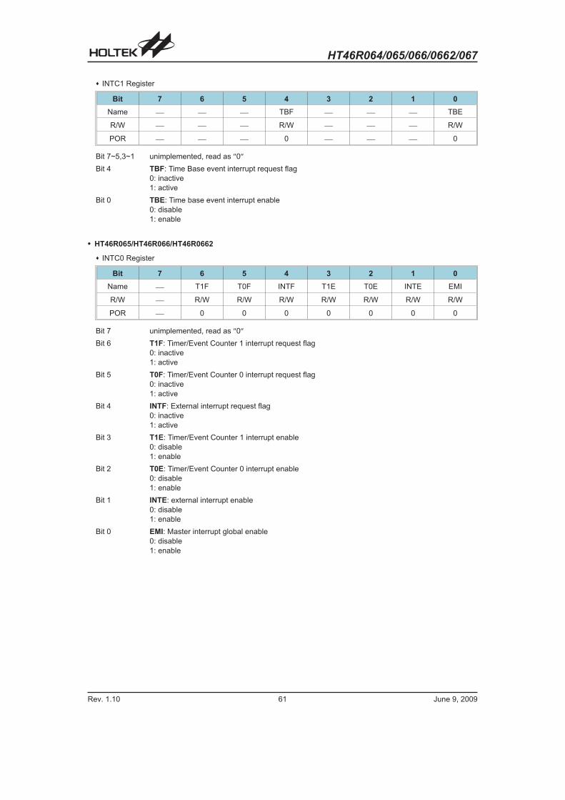
HT46R064/065/066/0662/067
Rev. 1.10 61 June 9, 2009
� INTC1 Register
Bit 7 6 5 4 3 2 1 0
Name � � � TBF � � � TBE
R/W � � � R/W � � � R/W
POR � � � 0 � � � 0
Bit 7~5,3~1 unimplemented, read as �0�
Bit 4 TBF: Time Base event interrupt request flag
0: inactive
1: active
Bit 0 TBE: Time base event interrupt enable
0: disable
1: enable
� HT46R065/HT46R066/HT46R0662
� INTC0 Register
Bit 7 6 5 4 3 2 1 0
Name � T1F T0F INTF T1E T0E INTE EMI
R/W � R/W R/W R/W R/W R/W R/W R/W
POR � 0 0 0 0 0 0 0
Bit 7 unimplemented, read as �0�
Bit 6 T1F: Timer/Event Counter 1 interrupt request flag
0: inactive
1: active
Bit 5 T0F: Timer/Event Counter 0 interrupt request flag
0: inactive
1: active
Bit 4 INTF: External interrupt request flag
0: inactive
1: active
Bit 3 T1E: Timer/Event Counter 1 interrupt enable
0: disable
1: enable
Bit 2 T0E: Timer/Event Counter 0 interrupt enable
0: disable
1: enable
Bit 1 INTE: external interrupt enable
0: disable
1: enable
Bit 0 EMI: Master interrupt global enable
0: disable
1: enable
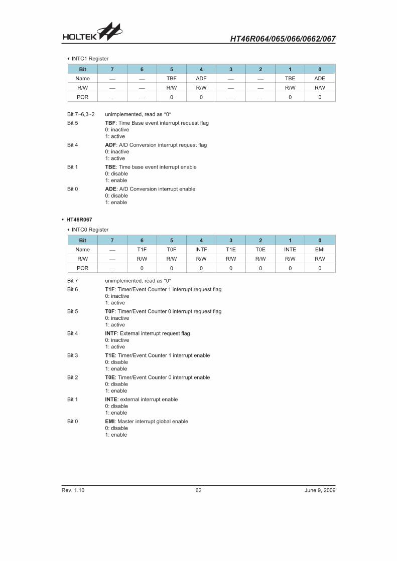
HT46R064/065/066/0662/067
Rev. 1.10 62 June 9, 2009
� INTC1 Register
Bit 7 6 5 4 3 2 1 0
Name � � TBF ADF � � TBE ADE
R/W � � R/W R/W � � R/W R/W
POR � � 0 0 � � 0 0
Bit 7~6,3~2 unimplemented, read as �0�
Bit 5 TBF: Time Base event interrupt request flag
0: inactive
1: active
Bit 4 ADF: A/D Conversion interrupt request flag
0: inactive
1: active
Bit 1 TBE: Time base event interrupt enable
0: disable
1: enable
Bit 0 ADE: A/D Conversion interrupt enable
0: disable
1: enable
� HT46R067
� INTC0 Register
Bit 7 6 5 4 3 2 1 0
Name � T1F T0F INTF T1E T0E INTE EMI
R/W � R/W R/W R/W R/W R/W R/W R/W
POR � 0 0 0 0 0 0 0
Bit 7 unimplemented, read as �0�
Bit 6 T1F: Timer/Event Counter 1 interrupt request flag
0: inactive
1: active
Bit 5 T0F: Timer/Event Counter 0 interrupt request flag
0: inactive
1: active
Bit 4 INTF: External interrupt request flag
0: inactive
1: active
Bit 3 T1E: Timer/Event Counter 1 interrupt enable
0: disable
1: enable
Bit 2 T0E: Timer/Event Counter 0 interrupt enable
0: disable
1: enable
Bit 1 INTE: external interrupt enable
0: disable
1: enable
Bit 0 EMI: Master interrupt global enable
0: disable
1: enable

HT46R064/065/066/0662/067
Rev. 1.10 63 June 9, 2009
� INTC1 Register
Bit 7 6 5 4 3 2 1 0
Name � TBF ADF T2F � TBE ADE T2E
R/W � R/W R/W R/W � R/W R/W R/W
POR � 0 0 0 � 0 0 0
Bit 7,3 unimplemented, read as �0�
Bit 6 TBF: Time Base event interrupt request flag
0: inactive
1: active
Bit 5 ADF: A/D Conversion interrupt request flag
0: inactive
1: active
Bit 4 T2F: Timer/Event Counter 2 interrupt request flag
0: inactive
1: active
Bit 2 TBE: Time base event interrupt enable
0: disable
1: enable
Bit 1 ADE: A/D Conversion interrupt enable
0: disable
1: enable
Bit 0 T2E: Timer/Event Counter 2 interrupt enable
0: disable
1: enable

HT46R064/065/066/0662/067
Rev. 1.10 64 June 9, 2009
Timer/Event Counter Interrupt
For a Timer/Event Counter interrupt to occur, the global
interrupt enable bit, EMI, and the corresponding timer
interrupt enable bit, TnE, must first be set. An actual
Timer/Event Counter interrupt will take place when the
Timer/Event Counter request flag, TnF, is set, a situation
that will occur when the relevant Timer/Event Counter
overflows. When the interrupt is enabled, the stack is
not full and a Timer/Event Counter n overflow occurs, a
subroutine call to the relevant timer interrupt vector, will
take place. When the interrupt is serviced, the timer in-
terrupt request flag, TnF, will be automatically reset and
the EMI bit will be automatically cleared to disable other
interrupts.
Time Base Interrupt
For a time base interrupt to occur the global interrupt en-
able bit EMI and the corresponding interrupt enable bit
TBE, must first be set. An actual Time Base interrupt will
take place when the time base request flag TBF is set, a
situation that will occur when the Time Base overflows.
When the interrupt is enabled, the stack is not full and a
time base overflow occurs a subroutine call to time base
vector will take place. When the interrupt is serviced, the
time base interrupt flag. TBF will be automatically reset
and the EMI bit will be automatically cleared to disable
other interrupts.
Programming Considerations
By disabling the interrupt enable bits, a requested inter-
rupt can be prevented from being serviced, however,
once an interrupt request flag is set, it will remain in this
condition in the interrupt register until the corresponding
interrupt is serviced or until the request flag is cleared by
a software instruction.
It is recommended that programs do not use the �CALL
subroutine� instruction within the interrupt subroutine.
Interrupts often occur in an unpredictable manner or
need to be serviced immediately in some applications. If
only one stack is left and the interrupt is not well con-
trolled, the original control sequence will be damaged
once a �CALL subroutine� is executed in the interrupt
subroutine.
All of these interrupts have the capability of waking up
the processor when in the Idle/Sleep Mode.
Only the Program Counter is pushed onto the stack. If
the contents of the register or status register are altered
by the interrupt service program, which may corrupt the
desired control sequence, then the contents should be
saved in advance.
SCOM Function for LCD
The devices have the capability of driving external LCD
panels. The common pins for LCD driving, SCOM0~
SCOM3, are pin shared with certain pin on the PB0~
PB3 port. The LCD signals (COM and SEG) are gener-
ated using the application program.
LCD Operation
An external LCD panel can be driven using this device
by configuring the PB0~PB3 pins as common pins and
using other output ports lines as segment pins. The LCD
driver function is controlled using the SCOMC register
which in addition to controlling the overall on/off function
also controls the bias voltage setup function. This en-
ables the LCD COM driver to generate the necessary
VDD/2 voltage levels for LCD 1/2 bias operation.
The SCOMEN bit in the SCOMC register is the overall
master control for the LCD Driver, however this bit is
used in conjunction with the COMnEN bits to select
which Port B pins are used for LCD driving. Note that the
Port Control register does not need to first setup the pins
as outputs to enable the LCD driver operation.
SCOMEN COMnEN Pin Function O/P Level
0 X I/O 0 or 1
1 0 I/O 0 or 1
1 1 SCOMN VDD/2
Output Control
+ � �
� � $ D
� � ,
� � * . � � * .
+ � � � &
� � � < � � � � � ! � 2 8 � � � �
LCD COM Bias

HT46R064/065/066/0662/067
Rev. 1.10 65 June 9, 2009
LCD Bias Control
The LCD COM driver enables a range of selections to be provided to suit the requirement of the LCD panel which is be-
ing used. The bias resistor choice is implemented using the ISEL1 and ISEL0 bits in the SCOMC register.
� SCOMC Register
Bit 7 6 5 4 3 2 1 0
Name � ISEL1 ISEL0 SCOMEN COM3EN COM2EN COM1EN COM0EN
R/W R/W R/W R/W R/W R/W R/W R/W R/W
POR 0 0 0 0 0 0 0 0
Bit 7 Reserved Bit
1: Unpredictable operation - bit must NOT be set high
0: Correct level - bit must be reset to zero for correct operation
Bit 6,5 ISEL1, ISEL0: SCOM operating current selection (VDD=5V)
00: 25�A
01: 50�A
10: 100�A
11: 200�A
Bit 4 SCOMEN: SCOM module on/off control
0: disable
1: enable
SCOMn can be enable by COMnEN if SCOMEN=1
Bit 3 COM3EN: PB3 or SCOM3 selection
0: GPIO
1: SCOM3
Bit 2 COM2EN: PB2 or SCOM2 selection
0: GPIO
1: SCOM2
Bit 1 COM1EN: PB1 or SCOM1 selection
0: GPIO
1: SCOM1
Bit 0 COM0EN: PB0 or SCOM0 selection
0: GPIO
1: SCOM0

Application Circuits
HT46R064/065/066/0662/067
Rev. 1.10 66 June 9, 2009
Configuration Options
Configuration options refer to certain options within the MCU that are programmed into the OTP Program Memory de-
vice during the programming process. During the development process, these options are selected using the HT-IDE
software development tools. As these options are programmed into the device using the hardware programming tools,
once they are selected they cannot be changed later by the application software. All options must be defined for proper
system function, the details of which are shown in the table.
No. Options
1 Watchdog Timer: enable or disable
2Watchdog Timer clock source: LXT, LIRC or fSYS/4
Note: LXT oscillator must be selected by OSC configuration option if WDT clock source is from LXT.
3 CLRWDT instructions: 1 or 2 instructions
4
(1)For HT46R064/HT46R065/HT46R066
System oscillator configuration: HXT, HIRC, ERC, HIRC + LXT
(2)For HT46R0662/HT46R067
System oscillator configuration: HXT, HIRC, ERC, HXT + LXT, HIRC + LXT, ERC + LXT
5 LVR function: enable or disable
6 LVR voltage: 2.1V, 3.15V or 4.2V
7 RES or PA7 pin function
8 SST: 1024 or 2 clocks (determine tSST for HIRC/ERC)
9 Internal RC: 4MHz, 8MHz or 12MHz
� (
� &
� � � 2 8 � �
� � % & ' $ $ � # � �� & # ' � "
� � $ � � . $
� � ( � � � � � � . (
� � & � � $ � � . &
� � , � � . � � � . ,
� � # � � ( � � � � $
� � $ D � � )
� & � � � � (� , � � � � &
� $ � � . #� ( � � . %� ' � � . '� ) � � . )
� � $ D � � )
� * $ D � * (
� � $ D � � (
1 � (
1 � &
� � � 2 8 � �
� � % & ' $ $ � # � �� & # ' � "
� * � � � )
+ � �
+
$ 4 ( � �
+ � �
� % #( ' � & ) ' #
$ 4 ( D ( � �
( $ ; � D
( $ $ ; �
, $ $ �
$ 4 $ ( � �
( . # ( # �

HT46R064/065/066/0662/067
Rev. 1.10 67 June 9, 2009
Instruction Set
Introduction
Central to the successful operat ion of any
microcontroller is its instruction set, which is a set of pro-
gram instruction codes that directs the microcontroller to
perform certain operations. In the case of Holtek
microcontrollers, a comprehensive and flexible set of
over 60 instructions is provided to enable programmers
to implement their application with the minimum of pro-
gramming overheads.
For easier understanding of the various instruction
codes, they have been subdivided into several func-
tional groupings.
Instruction Timing
Most instructions are implemented within one instruc-
tion cycle. The exceptions to this are branch, call, or ta-
ble read instructions where two instruction cycles are
required. One instruction cycle is equal to 4 system
clock cycles, therefore in the case of an 8MHz system
oscillator, most instructions would be implemented
within 0.5�s and branch or call instructions would be im-
plemented within 1�s. Although instructions which re-
quire one more cycle to implement are generally limited
to the JMP, CALL, RET, RETI and table read instruc-
tions, it is important to realize that any other instructions
which involve manipulation of the Program Counter Low
register or PCL will also take one more cycle to imple-
ment. As instructions which change the contents of the
PCL will imply a direct jump to that new address, one
more cycle will be required. Examples of such instruc-
tions would be �CLR PCL� or �MOV PCL, A�. For the
case of skip instructions, it must be noted that if the re-
sult of the comparison involves a skip operation then
this will also take one more cycle, if no skip is involved
then only one cycle is required.
Moving and Transferring Data
The transfer of data within the microcontroller program
is one of the most frequently used operations. Making
use of three kinds of MOV instructions, data can be
transferred from registers to the Accumulator and
vice-versa as well as being able to move specific imme-
diate data directly into the Accumulator. One of the most
important data transfer applications is to receive data
from the input ports and transfer data to the output ports.
Arithmetic Operations
The ability to perform certain arithmetic operations and
data manipulation is a necessary feature of most
microcontroller applications. Within the Holtek
microcontroller instruction set are a range of add and
subtract instruction mnemonics to enable the necessary
arithmetic to be carried out. Care must be taken to en-
sure correct handling of carry and borrow data when re-
sults exceed 255 for addition and less than 0 for
subtraction. The increment and decrement instructions
INC, INCA, DEC and DECA provide a simple means of
increasing or decreasing by a value of one of the values
in the destination specified.
Logical and Rotate Operations
The standard logical operations such as AND, OR, XOR
and CPL all have their own instruction within the Holtek
microcontroller instruction set. As with the case of most
instructions involving data manipulation, data must pass
through the Accumulator which may involve additional
programming steps. In all logical data operations, the
zero flag may be set if the result of the operation is zero.
Another form of logical data manipulation comes from
the rotate instructions such as RR, RL, RRC and RLC
which provide a simple means of rotating one bit right or
left. Different rotate instructions exist depending on pro-
gram requirements. Rotate instructions are useful for
serial port programming applications where data can be
rotated from an internal register into the Carry bit from
where it can be examined and the necessary serial bit
set high or low. Another application where rotate data
operations are used is to implement multiplication and
division calculations.
Branches and Control Transfer
Program branching takes the form of either jumps to
specified locations using the JMP instruction or to a sub-
routine using the CALL instruction. They differ in the
sense that in the case of a subroutine call, the program
must return to the instruction immediately when the sub-
routine has been carried out. This is done by placing a
return instruction RET in the subroutine which will cause
the program to jump back to the address right after the
CALL instruction. In the case of a JMP instruction, the
program simply jumps to the desired location. There is
no requirement to jump back to the original jumping off
point as in the case of the CALL instruction. One special
and extremely useful set of branch instructions are the
conditional branches. Here a decision is first made re-
garding the condition of a certain data memory or indi-
vidual bits. Depending upon the conditions, the program
will continue with the next instruction or skip over it and
jump to the following instruction. These instructions are
the key to decision making and branching within the pro-
gram perhaps determined by the condition of certain in-
put switches or by the condition of internal data bits.

HT46R064/065/066/0662/067
Rev. 1.10 68 June 9, 2009
Bit Operations
The ability to provide single bit operations on Data Mem-
ory is an extremely flexible feature of all Holtek
microcontrollers. This feature is especially useful for
output port bit programming where individual bits or port
pins can be directly set high or low using either the �SET
[m].i� or �CLR [m].i� instructions respectively. The fea-
ture removes the need for programmers to first read the
8-bit output port, manipulate the input data to ensure
that other bits are not changed and then output the port
with the correct new data. This read-modify-write pro-
cess is taken care of automatically when these bit oper-
ation instructions are used.
Table Read Operations
Data storage is normally implemented by using regis-
ters. However, when working with large amounts of
fixed data, the volume involved often makes it inconve-
nient to store the fixed data in the Data Memory. To over-
come this problem, Holtek microcontrollers allow an
area of Program Memory to be setup as a table where
data can be directly stored. A set of easy to use instruc-
tions provides the means by which this fixed data can be
referenced and retrieved from the Program Memory.
Other Operations
In addition to the above functional instructions, a range
of other instructions also exist such as the �HALT� in-
struction for Power-down operations and instructions to
control the operation of the Watchdog Timer for reliable
program operations under extreme electric or electro-
magnetic environments. For their relevant operations,
refer to the functional related sections.
Instruction Set Summary
The following table depicts a summary of the instruction
set categorised according to function and can be con-
sulted as a basic instruction reference using the follow-
ing listed conventions.
Table conventions:
x: Bits immediate data
m: Data Memory address
A: Accumulator
i: 0~7 number of bits
addr: Program memory address
Mnemonic Description Cycles Flag Affected
Arithmetic
ADD A,[m]
ADDM A,[m]
ADD A,x
ADC A,[m]
ADCM A,[m]
SUB A,x
SUB A,[m]
SUBM A,[m]
SBC A,[m]
SBCM A,[m]
DAA [m]
Add Data Memory to ACC
Add ACC to Data Memory
Add immediate data to ACC
Add Data Memory to ACC with Carry
Add ACC to Data memory with Carry
Subtract immediate data from the ACC
Subtract Data Memory from ACC
Subtract Data Memory from ACC with result in Data Memory
Subtract Data Memory from ACC with Carry
Subtract Data Memory from ACC with Carry, result in Data Memory
Decimal adjust ACC for Addition with result in Data Memory
1
1Note
1
1
1Note
1
1
1Note
1
1Note
1Note
Z, C, AC, OV
Z, C, AC, OV
Z, C, AC, OV
Z, C, AC, OV
Z, C, AC, OV
Z, C, AC, OV
Z, C, AC, OV
Z, C, AC, OV
Z, C, AC, OV
Z, C, AC, OV
C
Logic Operation
AND A,[m]
OR A,[m]
XOR A,[m]
ANDM A,[m]
ORM A,[m]
XORM A,[m]
AND A,x
OR A,x
XOR A,x
CPL [m]
CPLA [m]
Logical AND Data Memory to ACC
Logical OR Data Memory to ACC
Logical XOR Data Memory to ACC
Logical AND ACC to Data Memory
Logical OR ACC to Data Memory
Logical XOR ACC to Data Memory
Logical AND immediate Data to ACC
Logical OR immediate Data to ACC
Logical XOR immediate Data to ACC
Complement Data Memory
Complement Data Memory with result in ACC
1
1
1
1Note
1Note
1Note
1
1
1
1Note
1
Z
Z
Z
Z
Z
Z
Z
Z
Z
Z
Z
Increment & Decrement
INCA [m]
INC [m]
DECA [m]
DEC [m]
Increment Data Memory with result in ACC
Increment Data Memory
Decrement Data Memory with result in ACC
Decrement Data Memory
1
1Note
1
1Note
Z
Z
Z
Z

HT46R064/065/066/0662/067
Rev. 1.10 69 June 9, 2009
Mnemonic Description Cycles Flag Affected
Rotate
RRA [m]
RR [m]
RRCA [m]
RRC [m]
RLA [m]
RL [m]
RLCA [m]
RLC [m]
Rotate Data Memory right with result in ACC
Rotate Data Memory right
Rotate Data Memory right through Carry with result in ACC
Rotate Data Memory right through Carry
Rotate Data Memory left with result in ACC
Rotate Data Memory left
Rotate Data Memory left through Carry with result in ACC
Rotate Data Memory left through Carry
1
1Note
1
1Note
1
1Note
1
1Note
None
None
C
C
None
None
C
C
Data Move
MOV A,[m]
MOV [m],A
MOV A,x
Move Data Memory to ACC
Move ACC to Data Memory
Move immediate data to ACC
1
1Note
1
None
None
None
Bit Operation
CLR [m].i
SET [m].i
Clear bit of Data Memory
Set bit of Data Memory
1Note
1NoteNone
None
Branch
JMP addr
SZ [m]
SZA [m]
SZ [m].i
SNZ [m].i
SIZ [m]
SDZ [m]
SIZA [m]
SDZA [m]
CALL addr
RET
RET A,x
RETI
Jump unconditionally
Skip if Data Memory is zero
Skip if Data Memory is zero with data movement to ACC
Skip if bit i of Data Memory is zero
Skip if bit i of Data Memory is not zero
Skip if increment Data Memory is zero
Skip if decrement Data Memory is zero
Skip if increment Data Memory is zero with result in ACC
Skip if decrement Data Memory is zero with result in ACC
Subroutine call
Return from subroutine
Return from subroutine and load immediate data to ACC
Return from interrupt
2
1Note
1note
1Note
1Note
1Note
1Note
1Note
1Note
2
2
2
2
None
None
None
None
None
None
None
None
None
None
None
None
None
Table Read
TABRDC [m]
TABRDL [m]
Read table (current page) to TBLH and Data Memory
Read table (last page) to TBLH and Data Memory
2Note
2NoteNone
None
Miscellaneous
NOP
CLR [m]
SET [m]
CLR WDT
CLR WDT1
CLR WDT2
SWAP [m]
SWAPA [m]
HALT
No operation
Clear Data Memory
Set Data Memory
Clear Watchdog Timer
Pre-clear Watchdog Timer
Pre-clear Watchdog Timer
Swap nibbles of Data Memory
Swap nibbles of Data Memory with result in ACC
Enter power down mode
1
1Note
1Note
1
1
1
1Note
1
1
None
None
None
TO, PDF
TO, PDF
TO, PDF
None
None
TO, PDF
Note: 1. For skip instructions, if the result of the comparison involves a skip then two cycles are required,
if no skip takes place only one cycle is required.
2. Any instruction which changes the contents of the PCL will also require 2 cycles for execution.
3. For the �CLR WDT1� and �CLR WDT2� instructions the TO and PDF flags may be affected by
the execution status. The TO and PDF flags are cleared after both �CLR WDT1� and
�CLR WDT2� instructions are consecutively executed. Otherwise the TO and PDF flags
remain unchanged.
Instruction Definition
ADC A,[m] Add Data Memory to ACC with Carry
Description The contents of the specified Data Memory, Accumulator and the carry flag are added. The
result is stored in the Accumulator.
Operation ACC � ACC + [m] + C
Affected flag(s) OV, Z, AC, C
ADCM A,[m] Add ACC to Data Memory with Carry
Description The contents of the specified Data Memory, Accumulator and the carry flag are added. The
result is stored in the specified Data Memory.
Operation [m] � ACC + [m] + C
Affected flag(s) OV, Z, AC, C
ADD A,[m] Add Data Memory to ACC
Description The contents of the specified Data Memory and the Accumulator are added. The result is
stored in the Accumulator.
Operation ACC � ACC + [m]
Affected flag(s) OV, Z, AC, C
ADD A,x Add immediate data to ACC
Description The contents of the Accumulator and the specified immediate data are added. The result is
stored in the Accumulator.
Operation ACC � ACC + x
Affected flag(s) OV, Z, AC, C
ADDM A,[m] Add ACC to Data Memory
Description The contents of the specified Data Memory and the Accumulator are added. The result is
stored in the specified Data Memory.
Operation [m] � ACC + [m]
Affected flag(s) OV, Z, AC, C
AND A,[m] Logical AND Data Memory to ACC
Description Data in the Accumulator and the specified Data Memory perform a bitwise logical AND op-
eration. The result is stored in the Accumulator.
Operation ACC � ACC �AND� [m]
Affected flag(s) Z
AND A,x Logical AND immediate data to ACC
Description Data in the Accumulator and the specified immediate data perform a bitwise logical AND
operation. The result is stored in the Accumulator.
Operation ACC � ACC �AND� x
Affected flag(s) Z
ANDM A,[m] Logical AND ACC to Data Memory
Description Data in the specified Data Memory and the Accumulator perform a bitwise logical AND op-
eration. The result is stored in the Data Memory.
Operation [m] � ACC �AND� [m]
Affected flag(s) Z
HT46R064/065/066/0662/067
Rev. 1.10 70 June 9, 2009

CALL addr Subroutine call
Description Unconditionally calls a subroutine at the specified address. The Program Counter then in-
crements by 1 to obtain the address of the next instruction which is then pushed onto the
stack. The specified address is then loaded and the program continues execution from this
new address. As this instruction requires an additional operation, it is a two cycle instruc-
tion.
Operation Stack � Program Counter + 1
Program Counter � addr
Affected flag(s) None
CLR [m] Clear Data Memory
Description Each bit of the specified Data Memory is cleared to 0.
Operation [m] � 00H
Affected flag(s) None
CLR [m].i Clear bit of Data Memory
Description Bit i of the specified Data Memory is cleared to 0.
Operation [m].i � 0
Affected flag(s) None
CLR WDT Clear Watchdog Timer
Description The TO, PDF flags and the WDT are all cleared.
Operation WDT cleared
TO � 0
PDF � 0
Affected flag(s) TO, PDF
CLR WDT1 Pre-clear Watchdog Timer
Description The TO, PDF flags and the WDT are all cleared. Note that this instruction works in conjunc-
tion with CLR WDT2 and must be executed alternately with CLR WDT2 to have effect. Re-
petitively executing this instruction without alternately executing CLR WDT2 will have no
effect.
Operation WDT cleared
TO � 0
PDF � 0
Affected flag(s) TO, PDF
CLR WDT2 Pre-clear Watchdog Timer
Description The TO, PDF flags and the WDT are all cleared. Note that this instruction works in conjunc-
tion with CLR WDT1 and must be executed alternately with CLR WDT1 to have effect. Re-
petitively executing this instruction without alternately executing CLR WDT1 will have no
effect.
Operation WDT cleared
TO � 0
PDF � 0
Affected flag(s) TO, PDF
HT46R064/065/066/0662/067
Rev. 1.10 71 June 9, 2009

CPL [m] Complement Data Memory
Description Each bit of the specified Data Memory is logically complemented (1s complement). Bits
which previously contained a 1 are changed to 0 and vice versa.
Operation [m] � [m]
Affected flag(s) Z
CPLA [m] Complement Data Memory with result in ACC
Description Each bit of the specified Data Memory is logically complemented (1s complement). Bits
which previously contained a 1 are changed to 0 and vice versa. The complemented result
is stored in the Accumulator and the contents of the Data Memory remain unchanged.
Operation ACC � [m]
Affected flag(s) Z
DAA [m] Decimal-Adjust ACC for addition with result in Data Memory
Description Convert the contents of the Accumulator value to a BCD ( Binary Coded Decimal) value re-
sulting from the previous addition of two BCD variables. If the low nibble is greater than 9 or
if AC flag is set, then a value of 6 will be added to the low nibble. Otherwise the low nibble
remains unchanged. If the high nibble is greater than 9 or if the C flag is set, then a value of
6 will be added to the high nibble. Essentially, the decimal conversion is performed by add-
ing 00H, 06H, 60H or 66H depending on the Accumulator and flag conditions. Only the C
flag may be affected by this instruction which indicates that if the original BCD sum is
greater than 100, it allows multiple precision decimal addition.
Operation [m] � ACC + 00H or
[m] � ACC + 06H or
[m] � ACC + 60H or
[m] � ACC + 66H
Affected flag(s) C
DEC [m] Decrement Data Memory
Description Data in the specified Data Memory is decremented by 1.
Operation [m] � [m] � 1
Affected flag(s) Z
DECA [m] Decrement Data Memory with result in ACC
Description Data in the specified Data Memory is decremented by 1. The result is stored in the Accu-
mulator. The contents of the Data Memory remain unchanged.
Operation ACC � [m] � 1
Affected flag(s) Z
HALT Enter power down mode
Description This instruction stops the program execution and turns off the system clock. The contents
of the Data Memory and registers are retained. The WDT and prescaler are cleared. The
power down flag PDF is set and the WDT time-out flag TO is cleared.
Operation TO � 0
PDF � 1
Affected flag(s) TO, PDF
HT46R064/065/066/0662/067
Rev. 1.10 72 June 9, 2009

INC [m] Increment Data Memory
Description Data in the specified Data Memory is incremented by 1.
Operation [m] � [m] + 1
Affected flag(s) Z
INCA [m] Increment Data Memory with result in ACC
Description Data in the specified Data Memory is incremented by 1. The result is stored in the Accumu-
lator. The contents of the Data Memory remain unchanged.
Operation ACC � [m] + 1
Affected flag(s) Z
JMP addr Jump unconditionally
Description The contents of the Program Counter are replaced with the specified address. Program
execution then continues from this new address. As this requires the insertion of a dummy
instruction while the new address is loaded, it is a two cycle instruction.
Operation Program Counter � addr
Affected flag(s) None
MOV A,[m] Move Data Memory to ACC
Description The contents of the specified Data Memory are copied to the Accumulator.
Operation ACC � [m]
Affected flag(s) None
MOV A,x Move immediate data to ACC
Description The immediate data specified is loaded into the Accumulator.
Operation ACC � x
Affected flag(s) None
MOV [m],A Move ACC to Data Memory
Description The contents of the Accumulator are copied to the specified Data Memory.
Operation [m] � ACC
Affected flag(s) None
NOP No operation
Description No operation is performed. Execution continues with the next instruction.
Operation No operation
Affected flag(s) None
OR A,[m] Logical OR Data Memory to ACC
Description Data in the Accumulator and the specified Data Memory perform a bitwise logical OR oper-
ation. The result is stored in the Accumulator.
Operation ACC � ACC �OR� [m]
Affected flag(s) Z
HT46R064/065/066/0662/067
Rev. 1.10 73 June 9, 2009

OR A,x Logical OR immediate data to ACC
Description Data in the Accumulator and the specified immediate data perform a bitwise logical OR op-
eration. The result is stored in the Accumulator.
Operation ACC � ACC �OR� x
Affected flag(s) Z
ORM A,[m] Logical OR ACC to Data Memory
Description Data in the specified Data Memory and the Accumulator perform a bitwise logical OR oper-
ation. The result is stored in the Data Memory.
Operation [m] � ACC �OR� [m]
Affected flag(s) Z
RET Return from subroutine
Description The Program Counter is restored from the stack. Program execution continues at the re-
stored address.
Operation Program Counter � Stack
Affected flag(s) None
RET A,x Return from subroutine and load immediate data to ACC
Description The Program Counter is restored from the stack and the Accumulator loaded with the
specified immediate data. Program execution continues at the restored address.
Operation Program Counter � Stack
ACC � x
Affected flag(s) None
RETI Return from interrupt
Description The Program Counter is restored from the stack and the interrupts are re-enabled by set-
ting the EMI bit. EMI is the master interrupt global enable bit. If an interrupt was pending
when the RETI instruction is executed, the pending Interrupt routine will be processed be-
fore returning to the main program.
Operation Program Counter � Stack
EMI � 1
Affected flag(s) None
RL [m] Rotate Data Memory left
Description The contents of the specified Data Memory are rotated left by 1 bit with bit 7 rotated into bit
0.
Operation [m].(i+1) � [m].i; (i = 0~6)
[m].0 � [m].7
Affected flag(s) None
RLA [m] Rotate Data Memory left with result in ACC
Description The contents of the specified Data Memory are rotated left by 1 bit with bit 7 rotated into bit
0. The rotated result is stored in the Accumulator and the contents of the Data Memory re-
main unchanged.
Operation ACC.(i+1) � [m].i; (i = 0~6)
ACC.0 � [m].7
Affected flag(s) None
HT46R064/065/066/0662/067
Rev. 1.10 74 June 9, 2009

RLC [m] Rotate Data Memory left through Carry
Description The contents of the specified Data Memory and the carry flag are rotated left by 1 bit. Bit 7
replaces the Carry bit and the original carry flag is rotated into bit 0.
Operation [m].(i+1) � [m].i; (i = 0~6)
[m].0 � C
C � [m].7
Affected flag(s) C
RLCA [m] Rotate Data Memory left through Carry with result in ACC
Description Data in the specified Data Memory and the carry flag are rotated left by 1 bit. Bit 7 replaces
the Carry bit and the original carry flag is rotated into the bit 0. The rotated result is stored in
the Accumulator and the contents of the Data Memory remain unchanged.
Operation ACC.(i+1) � [m].i; (i = 0~6)
ACC.0 � C
C � [m].7
Affected flag(s) C
RR [m] Rotate Data Memory right
Description The contents of the specified Data Memory are rotated right by 1 bit with bit 0 rotated into
bit 7.
Operation [m].i � [m].(i+1); (i = 0~6)
[m].7 � [m].0
Affected flag(s) None
RRA [m] Rotate Data Memory right with result in ACC
Description Data in the specified Data Memory and the carry flag are rotated right by 1 bit with bit 0 ro-
tated into bit 7. The rotated result is stored in the Accumulator and the contents of the Data
Memory remain unchanged.
Operation ACC.i � [m].(i+1); (i = 0~6)
ACC.7 � [m].0
Affected flag(s) None
RRC [m] Rotate Data Memory right through Carry
Description The contents of the specified Data Memory and the carry flag are rotated right by 1 bit. Bit 0
replaces the Carry bit and the original carry flag is rotated into bit 7.
Operation [m].i � [m].(i+1); (i = 0~6)
[m].7 � C
C � [m].0
Affected flag(s) C
RRCA [m] Rotate Data Memory right through Carry with result in ACC
Description Data in the specified Data Memory and the carry flag are rotated right by 1 bit. Bit 0 re-
places the Carry bit and the original carry flag is rotated into bit 7. The rotated result is
stored in the Accumulator and the contents of the Data Memory remain unchanged.
Operation ACC.i � [m].(i+1); (i = 0~6)
ACC.7 � C
C � [m].0
Affected flag(s) C
HT46R064/065/066/0662/067
Rev. 1.10 75 June 9, 2009

SBC A,[m] Subtract Data Memory from ACC with Carry
Description The contents of the specified Data Memory and the complement of the carry flag are sub-
tracted from the Accumulator. The result is stored in the Accumulator. Note that if the result
of subtraction is negative, the C flag will be cleared to 0, otherwise if the result is positive or
zero, the C flag will be set to 1.
Operation ACC � ACC � [m] � C
Affected flag(s) OV, Z, AC, C
SBCM A,[m] Subtract Data Memory from ACC with Carry and result in Data Memory
Description The contents of the specified Data Memory and the complement of the carry flag are sub-
tracted from the Accumulator. The result is stored in the Data Memory. Note that if the re-
sult of subtraction is negative, the C flag will be cleared to 0, otherwise if the result is
positive or zero, the C flag will be set to 1.
Operation [m] � ACC � [m] � C
Affected flag(s) OV, Z, AC, C
SDZ [m] Skip if decrement Data Memory is 0
Description The contents of the specified Data Memory are first decremented by 1. If the result is 0 the
following instruction is skipped. As this requires the insertion of a dummy instruction while
the next instruction is fetched, it is a two cycle instruction. If the result is not 0 the program
proceeds with the following instruction.
Operation [m] � [m] � 1
Skip if [m] = 0
Affected flag(s) None
SDZA [m] Skip if decrement Data Memory is zero with result in ACC
Description The contents of the specified Data Memory are first decremented by 1. If the result is 0, the
following instruction is skipped. The result is stored in the Accumulator but the specified
Data Memory contents remain unchanged. As this requires the insertion of a dummy in-
struction while the next instruction is fetched, it is a two cycle instruction. If the result is not
0, the program proceeds with the following instruction.
Operation ACC � [m] � 1
Skip if ACC = 0
Affected flag(s) None
SET [m] Set Data Memory
Description Each bit of the specified Data Memory is set to 1.
Operation [m] � FFH
Affected flag(s) None
SET [m].i Set bit of Data Memory
Description Bit i of the specified Data Memory is set to 1.
Operation [m].i � 1
Affected flag(s) None
HT46R064/065/066/0662/067
Rev. 1.10 76 June 9, 2009

SIZ [m] Skip if increment Data Memory is 0
Description The contents of the specified Data Memory are first incremented by 1. If the result is 0, the
following instruction is skipped. As this requires the insertion of a dummy instruction while
the next instruction is fetched, it is a two cycle instruction. If the result is not 0 the program
proceeds with the following instruction.
Operation [m] � [m] + 1
Skip if [m] = 0
Affected flag(s) None
SIZA [m] Skip if increment Data Memory is zero with result in ACC
Description The contents of the specified Data Memory are first incremented by 1. If the result is 0, the
following instruction is skipped. The result is stored in the Accumulator but the specified
Data Memory contents remain unchanged. As this requires the insertion of a dummy in-
struction while the next instruction is fetched, it is a two cycle instruction. If the result is not
0 the program proceeds with the following instruction.
Operation ACC � [m] + 1
Skip if ACC = 0
Affected flag(s) None
SNZ [m].i Skip if bit i of Data Memory is not 0
Description If bit i of the specified Data Memory is not 0, the following instruction is skipped. As this re-
quires the insertion of a dummy instruction while the next instruction is fetched, it is a two
cycle instruction. If the result is 0 the program proceeds with the following instruction.
Operation Skip if [m].i 0
Affected flag(s) None
SUB A,[m] Subtract Data Memory from ACC
Description The specified Data Memory is subtracted from the contents of the Accumulator. The result
is stored in the Accumulator. Note that if the result of subtraction is negative, the C flag will
be cleared to 0, otherwise if the result is positive or zero, the C flag will be set to 1.
Operation ACC � ACC � [m]
Affected flag(s) OV, Z, AC, C
SUBM A,[m] Subtract Data Memory from ACC with result in Data Memory
Description The specified Data Memory is subtracted from the contents of the Accumulator. The result
is stored in the Data Memory. Note that if the result of subtraction is negative, the C flag will
be cleared to 0, otherwise if the result is positive or zero, the C flag will be set to 1.
Operation [m] � ACC � [m]
Affected flag(s) OV, Z, AC, C
SUB A,x Subtract immediate data from ACC
Description The immediate data specified by the code is subtracted from the contents of the Accumu-
lator. The result is stored in the Accumulator. Note that if the result of subtraction is nega-
tive, the C flag will be cleared to 0, otherwise if the result is positive or zero, the C flag will
be set to 1.
Operation ACC � ACC � x
Affected flag(s) OV, Z, AC, C
HT46R064/065/066/0662/067
Rev. 1.10 77 June 9, 2009

SWAP [m] Swap nibbles of Data Memory
Description The low-order and high-order nibbles of the specified Data Memory are interchanged.
Operation [m].3~[m].0 � [m].7 ~ [m].4
Affected flag(s) None
SWAPA [m] Swap nibbles of Data Memory with result in ACC
Description The low-order and high-order nibbles of the specified Data Memory are interchanged. The
result is stored in the Accumulator. The contents of the Data Memory remain unchanged.
Operation ACC.3 ~ ACC.0 � [m].7 ~ [m].4
ACC.7 ~ ACC.4 � [m].3 ~ [m].0
Affected flag(s) None
SZ [m] Skip if Data Memory is 0
Description If the contents of the specified Data Memory is 0, the following instruction is skipped. As
this requires the insertion of a dummy instruction while the next instruction is fetched, it is a
two cycle instruction. If the result is not 0 the program proceeds with the following instruc-
tion.
Operation Skip if [m] = 0
Affected flag(s) None
SZA [m] Skip if Data Memory is 0 with data movement to ACC
Description The contents of the specified Data Memory are copied to the Accumulator. If the value is
zero, the following instruction is skipped. As this requires the insertion of a dummy instruc-
tion while the next instruction is fetched, it is a two cycle instruction. If the result is not 0 the
program proceeds with the following instruction.
Operation ACC � [m]
Skip if [m] = 0
Affected flag(s) None
SZ [m].i Skip if bit i of Data Memory is 0
Description If bit i of the specified Data Memory is 0, the following instruction is skipped. As this re-
quires the insertion of a dummy instruction while the next instruction is fetched, it is a two
cycle instruction. If the result is not 0, the program proceeds with the following instruction.
Operation Skip if [m].i = 0
Affected flag(s) None
TABRDC [m] Read table (current page) to TBLH and Data Memory
Description The low byte of the program code (current page) addressed by the table pointer (TBLP) is
moved to the specified Data Memory and the high byte moved to TBLH.
Operation [m] � program code (low byte)
TBLH � program code (high byte)
Affected flag(s) None
TABRDL [m] Read table (last page) to TBLH and Data Memory
Description The low byte of the program code (last page) addressed by the table pointer (TBLP) is
moved to the specified Data Memory and the high byte moved to TBLH.
Operation [m] � program code (low byte)
TBLH � program code (high byte)
Affected flag(s) None
HT46R064/065/066/0662/067
Rev. 1.10 78 June 9, 2009

XOR A,[m] Logical XOR Data Memory to ACC
Description Data in the Accumulator and the specified Data Memory perform a bitwise logical XOR op-
eration. The result is stored in the Accumulator.
Operation ACC � ACC �XOR� [m]
Affected flag(s) Z
XORM A,[m] Logical XOR ACC to Data Memory
Description Data in the specified Data Memory and the Accumulator perform a bitwise logical XOR op-
eration. The result is stored in the Data Memory.
Operation [m] � ACC �XOR� [m]
Affected flag(s) Z
XOR A,x Logical XOR immediate data to ACC
Description Data in the Accumulator and the specified immediate data perform a bitwise logical XOR
operation. The result is stored in the Accumulator.
Operation ACC � ACC �XOR� x
Affected flag(s) Z
HT46R064/065/066/0662/067
Rev. 1.10 79 June 9, 2009

Package Information
16-pin DIP (300mil) Outline Dimensions
� MS-001d (see fig1)
SymbolDimensions in mil
Min. Nom. Max.
A 780 � 880
B 240 � 280
C 115 � 195
D 115 � 150
E 14 � 22
F 45 � 70
G � 100 �
H 300 � 325
I � � 430
� MS-001d (see fig2)
SymbolDimensions in mil
Min. Nom. Max.
A 735 � 775
B 240 � 280
C 115 � 195
D 115 � 150
E 14 � 22
F 45 � 70
G � 100 �
H 300 � 325
I � � 430
HT46R064/065/066/0662/067
Rev. 1.10 80 June 9, 2009
� �
( '
(
-
�
�
�
�
*
�
"
@
�
Fig1. Full Lead Packages
� �
( '
(
-
�
�
�
�
*
�
"
@
�
Fig2. 1/2 Lead Packages

� MO-095a (see fig2)
SymbolDimensions in mil
Min. Nom. Max.
A 745 � 785
B 275 � 295
C 120 � 150
D 110 � 150
E 14 � 22
F 45 � 60
G � 100 �
H 300 � 325
I � � 430
HT46R064/065/066/0662/067
Rev. 1.10 81 June 9, 2009

16-pin NSOP (150mil) Outline Dimensions
SymbolDimensions in mil
Min. Nom. Max.
A 228 � 244
B 149 � 157
C 14 � 20
C 386 � 394
D 53 � 69
E � 50 �
F 4 � 10
G 22 � 28
H 4 � 12
� 0 � 10
HT46R064/065/066/0662/067
Rev. 1.10 82 June 9, 2009
( '
(
-
�
�
� �
�
* �
"
@
L

20-pin DIP (300mil) Outline Dimensions
� MS-001d (see fig1)
SymbolDimensions in mil
Min. Nom. Max.
A 980 � 1060
B 240 � 280
C 115 � 195
D 115 � 150
E 14 � 22
F 45 � 70
G � 100 �
H 300 � 325
I � � 430
� MO-095a (see fig2)
SymbolDimensions in mil
Min. Nom. Max.
A 945 � 985
B 275 � 295
C 120 � 150
D 110 � 150
E 14 � 22
F 45 � 60
G � 100 �
H 300 � 325
I � � 430
HT46R064/065/066/0662/067
Rev. 1.10 83 June 9, 2009
& $
(
( (
( $
�
�
�
* � "
@
�
Fig1. Full Lead Packages
& $
(
( (
( $
�
�
�
* � "
@
�
Fig2. 1/2 Lead Packages

20-pin SOP (300mil) Outline Dimensions
� MS-013
SymbolDimensions in mil
Min. Nom. Max.
A 393 � 419
B 256 � 300
C 12 � 20
C 496 � 512
D � � 104
E � 50 �
F 4 � 12
G 16 � 50
H 8 � 13
� 0 � 8
HT46R064/065/066/0662/067
Rev. 1.10 84 June 9, 2009
& $
(
( (
( $
� �
�
* �
L"
@
�

20-pin SSOP (150mil) Outline Dimensions
SymbolDimensions in mil
Min. Nom. Max.
A 228 � 244
B 150 � 158
C 8 � 12
C 335 � 347
D 49 � 65
E � 25 �
F 4 � 10
G 15 � 50
H 7 � 10
� 0 � 8
HT46R064/065/066/0662/067
Rev. 1.10 85 June 9, 2009
& $
(
( (
( $
� �
�
* �
L"
@
�

24-pin SKDIP (300mil) Outline Dimensions
� MS-001d (see fig1)
SymbolDimensions in mil
Min. Nom. Max.
A 1230 � 1280
B 240 � 280
C 115 � 195
D 115 � 150
E 14 � 22
F 45 � 70
G � 100 �
H 300 � 325
I � � 430
� MS-001d (see fig2)
SymbolDimensions in mil
Min. Nom. Max.
A 1160 � 1195
B 240 � 280
C 115 � 195
D 115 � 150
E 14 � 22
F 45 � 70
G � 100 �
H 300 � 325
I � � 430
HT46R064/065/066/0662/067
Rev. 1.10 86 June 9, 2009
& #
(
( ,
( &
�
�
�
* � "
@
�
Fig1. Full Lead Packages
& #
(
( ,
( &
�
�
�
* � "
@
�
Fig2. 1/2 Lead Packages
� MO-095a (see fig2)
SymbolDimensions in mil
Min. Nom. Max.
A 1145 � 1185
B 275 � 295
C 120 � 150
D 110 � 150
E 14 � 22
F 45 � 60
G � 100 �
H 300 � 325
I � � 430
HT46R064/065/066/0662/067
Rev. 1.10 87 June 9, 2009

24-pin SOP (300mil) Outline Dimensions
� MS-013
SymbolDimensions in mil
Min. Nom. Max.
A 393 � 419
B 256 � 300
C 12 � 20
C 598 � 613
D � � 104
E � 50 �
F 4 � 12
G 16 � 50
H 8 � 13
� 0 � 8
HT46R064/065/066/0662/067
Rev. 1.10 88 June 9, 2009
& #
(
( ,
( &
� �
�
* �
L"
@
�

24-pin SSOP (150mil) Outline Dimensions
SymbolDimensions in mil
Min. Nom. Max.
A 228 � 244
B 150 � 157
C 8 � 12
C 335 � 346
D 54 � 60
E � 25 �
F 4 � 10
G 22 � 28
H 7 � 10
� 0 � 8
HT46R064/065/066/0662/067
Rev. 1.10 89 June 9, 2009
& #
(
( ,
( &
� �
�
* �
L"
@
�

28-pin SKDIP (300mil) Outline Dimensions
SymbolDimensions in mil
Min. Nom. Max.
A 1375 � 1395
B 278 � 298
C 125 � 135
D 125 � 145
E 16 � 20
F 50 � 70
G � 100 �
H 295 � 315
I � � 375
HT46R064/065/066/0662/067
Rev. 1.10 90 June 9, 2009
� �& �
(
( %
( #
�
�
�
* � "
@
�

28-pin SOP (300mil) Outline Dimensions
� MS-013
SymbolDimensions in mil
Min. Nom. Max.
A 393 � 419
B 256 � 300
C 12 � 20
C 697 � 713
D � � 104
E � 50 �
F 4 � 12
G 16 � 50
H 8 � 13
� 0 � 8
HT46R064/065/066/0662/067
Rev. 1.10 91 June 9, 2009
& �
(
( %
( #
� �
�
�
L"
@
�*

28-pin SSOP (150mil) Outline Dimensions
SymbolDimensions in mil
Min. Nom. Max.
A 228 � 244
B 150 � 157
C 8 � 12
C 386 � 394
D 54 � 60
E � 25 �
F 4 � 10
G 22 � 28
H 7 � 10
� 0 � 8
HT46R064/065/066/0662/067
Rev. 1.10 92 June 9, 2009
& �
(
( %
( #
� �
�
�
L"
@
�*

44-pin QFP (10mm�10mm) Outline Dimensions
SymbolDimensions in mm
Min. Nom. Max.
A 13.00 � 13.40
B 9.90 � 10.10
C 13.00 � 13.40
D 9.90 � 10.10
E � 0.80 �
F � 0.30 �
G 1.90 � 2.20
H � � 2.70
I 0.25 � 0.50
J 0.73 � 0.93
K 0.10 � 0.20
L � 0.10 �
� 0 � 7
HT46R064/065/066/0662/067
Rev. 1.10 93 June 9, 2009
, #
( ((
# #
� �
& &
( &
*
�
"
@
�
M
F �
, , & ,
�
�
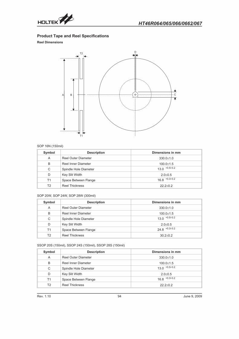
Product Tape and Reel Specifications
Reel Dimensions
SOP 16N (150mil)
Symbol Description Dimensions in mm
A Reel Outer Diameter 330.0�1.0
B Reel Inner Diameter 100.0�1.5
C Spindle Hole Diameter 13.0 +0.5/-0.2
D Key Slit Width 2.0�0.5
T1 Space Between Flange 16.8 +0.3/-0.2
T2 Reel Thickness 22.2�0.2
SOP 20W, SOP 24W, SOP 28W (300mil)
Symbol Description Dimensions in mm
A Reel Outer Diameter 330.0�1.0
B Reel Inner Diameter 100.0�1.5
C Spindle Hole Diameter 13.0 +0.5/-0.2
D Key Slit Width 2.0�0.5
T1 Space Between Flange 24.8 +0.3/-0.2
T2 Reel Thickness 30.2�0.2
SSOP 20S (150mil), SSOP 24S (150mil), SSOP 28S (150mil)
Symbol Description Dimensions in mm
A Reel Outer Diameter 330.0�1.0
B Reel Inner Diameter 100.0�1.5
C Spindle Hole Diameter 13.0 +0.5/-0.2
D Key Slit Width 2.0�0.5
T1 Space Between Flange 16.8 +0.3/-0.2
T2 Reel Thickness 22.2�0.2
HT46R064/065/066/0662/067
Rev. 1.10 94 June 9, 2009
� �
� (
� &�

Carrier Tape Dimensions
SOP 16N (150mil)
Symbol Description Dimensions in mm
W Carrier Tape Width 16.0�0.3
P Cavity Pitch 8.0�0.1
E Perforation Position 1.75�0.1
F Cavity to Perforation (Width Direction) 7.5�0.1
D Perforation Diameter 1.55 +0.10/-0.00
D1 Cavity Hole Diameter 1.50 +0.25/-0.00
P0 Perforation Pitch 4.0�0.1
P1 Cavity to Perforation (Length Direction) 2.0�0.1
A0 Cavity Length 6.5�0.1
B0 Cavity Width 10.3�0.1
K0 Cavity Depth 2.1�0.1
t Carrier Tape Thickness 0.30�0.05
C Cover Tape Width 13.3�0.1
SOP 20W
Symbol Description Dimensions in mm
W Carrier Tape Width 24.0 +0.3/-0.1
P Cavity Pitch 12.0�0.1
E Perforation Position 1.75�0.10
F Cavity to Perforation (Width Direction) 11.5�0.1
D Perforation Diameter 1.5 +0.1/-0.0
D1 Cavity Hole Diameter 1.50 +0.25/-0.00
P0 Perforation Pitch 4.0�0.1
P1 Cavity to Perforation (Length Direction) 2.0�0.1
A0 Cavity Length 10.8�0.1
B0 Cavity Width 13.3�0.1
K0 Cavity Depth 3.2�0.1
t Carrier Tape Thickness 0.30�0.05
C Cover Tape Width 21.3�0.1
HT46R064/065/066/0662/067
Rev. 1.10 95 June 9, 2009
�� (
�
� (� $�
*
�
�
F $
� $
� $
� � < � 2 ; � ! � � < � � ( � � B � � 3 � � � � � : � 3 : � �� � � � : 2 � � � B � � � 3 � � � � � � � � � B � 4
� � � : � @ : �

SOP 24W
Symbol Description Dimensions in mm
W Carrier Tape Width 24.0�0.3
P Cavity Pitch 12.0�0.1
E Perforation Position 1.75�0.1
F Cavity to Perforation (Width Direction) 11.5�0.1
D Perforation Diameter 1.55 +0.10/-0.00
D1 Cavity Hole Diameter 1.50 +0.25/-0.00
P0 Perforation Pitch 4.0�0.1
P1 Cavity to Perforation (Length Direction) 2.0�0.1
A0 Cavity Length 10.9�0.1
B0 Cavity Width 15.9�0.1
K0 Cavity Depth 3.1�0.1
t Carrier Tape Thickness 0.35�0.05
C Cover Tape Width 21.3�0.1
SOP 28W (300mil)
Symbol Description Dimensions in mm
W Carrier Tape Width 24.0�0.3
P Cavity Pitch 12.0�0.1
E Perforation Position 1.75�0.10
F Cavity to Perforation (Width Direction) 11.5�0.1
D Perforation Diameter 1.5 +0.1/-0.0
D1 Cavity Hole Diameter 1.50 +0.25/-0.00
P0 Perforation Pitch 4.0�0.1
P1 Cavity to Perforation (Length Direction) 2.0�0.1
A0 Cavity Length 10.85�0.10
B0 Cavity Width 18.34�0.10
K0 Cavity Depth 2.97�0.10
t Carrier Tape Thickness 0.35�0.01
C Cover Tape Width 21.3�0.1
HT46R064/065/066/0662/067
Rev. 1.10 96 June 9, 2009
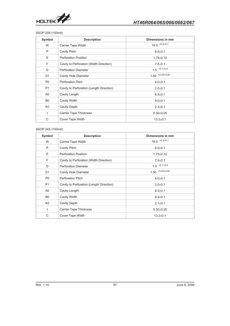
SSOP 20S (150mil)
Symbol Description Dimensions in mm
W Carrier Tape Width 16.0 +0.3/-0.1
P Cavity Pitch 8.0�0.1
E Perforation Position 1.75�0.10
F Cavity to Perforation (Width Direction) 7.5�0.1
D Perforation Diameter 1.5 +0.1/-0.0
D1 Cavity Hole Diameter 1.50 +0.25/-0.00
P0 Perforation Pitch 4.0�0.1
P1 Cavity to Perforation (Length Direction) 2.0�0.1
A0 Cavity Length 6.5�0.1
B0 Cavity Width 9.0�0.1
K0 Cavity Depth 2.3�0.1
t Carrier Tape Thickness 0.30�0.05
C Cover Tape Width 13.3�0.1
SSOP 24S (150mil)
Symbol Description Dimensions in mm
W Carrier Tape Width 16.0 +0.3/-0.1
P Cavity Pitch 8.0�0.1
E Perforation Position 1.75�0.10
F Cavity to Perforation (Width Direction) 7.5�0.1
D Perforation Diameter 1.5 +0.1/-0.0
D1 Cavity Hole Diameter 1.50 +0.25/-0.00
P0 Perforation Pitch 4.0�0.1
P1 Cavity to Perforation (Length Direction) 2.0�0.1
A0 Cavity Length 6.5�0.1
B0 Cavity Width 9.5�0.1
K0 Cavity Depth 2.1�0.1
t Carrier Tape Thickness 0.30�0.05
C Cover Tape Width 13.3�0.1
HT46R064/065/066/0662/067
Rev. 1.10 97 June 9, 2009

SSOP 28S (150mil)
Symbol Description Dimensions in mm
W Carrier Tape Width 16.0�0.3
P Cavity Pitch 8.0�0.1
E Perforation Position 1.75�0.1
F Cavity to Perforation (Width Direction) 7.5�0.1
D Perforation Diameter 1.55 +0.10/-0.00
D1 Cavity Hole Diameter 1.50 +0.25/-0.00
P0 Perforation Pitch 4.0�0.1
P1 Cavity to Perforation (Length Direction) 2.0�0.1
A0 Cavity Length 6.5�0.1
B0 Cavity Width 10.3�0.1
K0 Cavity Depth 2.1�0.1
t Carrier Tape Thickness 0.30�0.05
C Cover Tape Width 13.3�0.1
HT46R064/065/066/0662/067
Rev. 1.10 98 June 9, 2009

HT46R064/065/066/0662/067
Rev. 1.10 99 June 9, 2009
Copyright � 2009 by HOLTEK SEMICONDUCTOR INC.
The information appearing in this Data Sheet is believed to be accurate at the time of publication. However, Holtek as-sumes no responsibility arising from the use of the specifications described. The applications mentioned herein are usedsolely for the purpose of illustration and Holtek makes no warranty or representation that such applications will be suitablewithout further modification, nor recommends the use of its products for application that may present a risk to human life
due to malfunction or otherwise. Holteks products are not authorized for use as critical components in life support devicesor systems. Holtek reserves the right to alter its products without prior notification. For the most up-to-date information,please visit our web site at http://www.holtek.com.tw.
Holtek Semiconductor Inc. (Headquarters)No.3, Creation Rd. II, Science Park, Hsinchu, TaiwanTel: 886-3-563-1999Fax: 886-3-563-1189http://www.holtek.com.tw
Holtek Semiconductor Inc. (Taipei Sales Office)4F-2, No. 3-2, YuanQu St., Nankang Software Park, Taipei 115, TaiwanTel: 886-2-2655-7070Fax: 886-2-2655-7373Fax: 886-2-2655-7383 (International sales hotline)
Holtek Semiconductor Inc. (Shanghai Sales Office)G Room, 3 Floor, No.1 Building, No.2016 Yi-Shan Road, Minhang District, Shanghai, China 201103Tel: 86-21-5422-4590Fax: 86-21-5422-4705http://www.holtek.com.cn
Holtek Semiconductor Inc. (Shenzhen Sales Office)5F, Unit A, Productivity Building, No.5 Gaoxin M 2nd Road, Nanshan District, Shenzhen, China 518057Tel: 86-755-8616-9908, 86-755-8616-9308Fax: 86-755-8616-9722
Holtek Semiconductor Inc. (Beijing Sales Office)Suite 1721, Jinyu Tower, A129 West Xuan Wu Men Street, Xicheng District, Beijing, China 100031Tel: 86-10-6641-0030, 86-10-6641-7751, 86-10-6641-7752Fax: 86-10-6641-0125
Holtek Semiconductor (USA), Inc. (North America Sales Office)46729 Fremont Blvd., Fremont, CA 94538, USATel: 1-510-252-9880Fax: 1-510-252-9885http://www.holtek.com


![CSEPEl PANNONIA IS]shveiprom.com/cats/SCHMETZ/CHZEPEL-PANNONIA-DURKOPP...DORKOPP ADLER £51 030-10 ALL CLASSES EXCEPT 067 TO 69 067 62 S 067-262 Z 067 272 NH 1 067-372 TO 373 067-1000](https://img.pdfslide.us/doc/110x75/60aa411c98eb557f2754c8e9/csepel-pannonia-is-dorkopp-adler-51-030-10-all-classes-except-067-to-69-067.jpg)
![[701-0662-00 L] Environmental Impacts, Threshold Levels ...701-0662-00L]Lecture10-Brink-Noise-Slides.pdf · • Exposure assessment in environmental epidemiology • Exposure-response](https://img.pdfslide.us/doc/110x75/5f0a958b7e708231d42c59c2/701-0662-00-l-environmental-impacts-threshold-levels-701-0662-00llecture10-brink-noise-.jpg)