Embed Size (px)
Citation preview
Rev. 1.00 1 November 22, 2011 Rev. 1.00 PB November 22, 2011
HT16C21RAM Mapping 20*4 / 16*8 LCD Driver Controller
Feature ● Operating voltage: 2.4 ~ 5.5V ● Internal 32kHz RC oscillator ● Bias: 1/3 or 1/4; Duty: 1/4 or 1/8 ● Internal LCD bias generation with voltage-
follower buffers ● I2C interface ● Two selectable LCD frame frequencies: 80Hz or
160Hz ● Up to 16 x 8 bits RAM for display data storage ● Display patterns:
– 20 x 4 patterns: 20 segments and 4 commons – 16 x 8 patterns: 16 segments and 8 commons
● Versatile blinking modes ● R/W address auto increment ● Internal 16-step voltage adjustment to adjust LCD
operating voltage ● Low power consumption ● Provides VLCD pin to adjust LCD operating voltage ● Manufactured in silicon gate CMOS process ● Package Type: 20/24/28 SOP, 16 NSOP and Chip.
Applications ● Electronic meter ● Water meter ● Gas meter ● Heat energy meter ● Household appliance ● Games ● Telephone ● Consumer electronics
General DescriptionThe HT16C21 device is a memory mapping and multi-function LCD controller/driver. The display segments of the device are 80 patterns (20 segments and 4 commons) or 128 patterns (16 segments and 8 commons). The software configuration feature of the HT16C21 device makes it suitable for multiple LCD applications including LCD modules and display subsystems. The HT16C21 device communicates with most microprocessors/microcontrollers via a two-line bidirectional I2C interface.
索取样品 快速开发 工程服务 技术支持 联系人:许先生 QQ:191 888 5898 TEL:188 9858 2398
Rev. 1.00 2 November 22, 2011
HT16C21
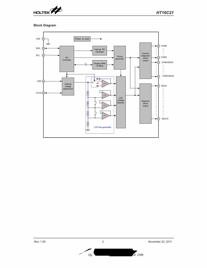
Block Diagram
LCD Voltage Selector
Column /Segment
driveroutput
Segment driveroutput
Display RAM16*8bits
Timing generatorI2C
Controller
COM0
COM3
SEG4
VLCD
VSS
SDA
SCL
Internal RC Oscillator
Power_on reset
R -
+OP1
COM4/SEG0
COM7/SEG3
R -
+OP2
SEG19
VDD
LCD bias generator
R
8
R -
+OP3
Internal voltage
adjustment
-
+OP4
索取样品 快速开发 工程服务 技术支持 联系人:许先生 QQ:191 888 5898 TEL:188 9858 2398
Rev. 1.00 3 November 22, 2011
HT16C21
Pin Assignment
24
23
22
21
20
19
18
17
16
15
14
13
1
2
3
4
5
6
7
8
9
10
11
12
VDDSDASCLVSS
COM0COM1COM2COM3
COM4/SEG0COM5/SEG1COM6/SEG2COM7/SEG3
SEG19/VLCDSEG18SEG15SEG14SEG13SEG12SEG11SEG10SEG7SEG6SEG5SEG4
16
15
14
13
12
11
10
9
1
2
3
4
5
6
7
8
VDDSDASCLVSS
COM0COM1COM2COM3
SEG19/VLCDSEG14SEG13SEG12COM7/SEG3COM6/SEG2COM5/SEG1COM4/SEG0
20
19
18
17
16
15
14
13
12
11
1
2
3
4
5
6
7
8
9
10
VDDSDASCLVSS
COM0COM1COM2COM3
COM4/SEG0COM5/SEG1
SEG19/VLCDSEG18SEG13SEG12SEG11SEG10SEG5SEG4COM7/SEG3COM6/SEG2
28
27
1
2
26
25
24
23
22
21
20
19
18
17
16
15
3
4
5
6
7
8
9
10
11
12
13
14
VDDSDASCLVSS
COM0COM1COM2COM3
COM4/SEG0COM5/SEG1COM6/SEG2COM7/SEG3
SEG4SEG5
SEG19/VLCDSEG18SEG17SEG16SEG15SEG14SEG13SEG12SEG11SEG10SEG9SEG8SEG7SEG6
HT16C2124 SOP-A
HT16C2128 SOP-A
HT16C2116 NSOP-A
HT16C2120 SOP-A
索取样品 快速开发 工程服务 技术支持 联系人:许先生 QQ:191 888 5898 TEL:188 9858 2398
Rev. 1.00 4 November 22, 2011
HT16C21
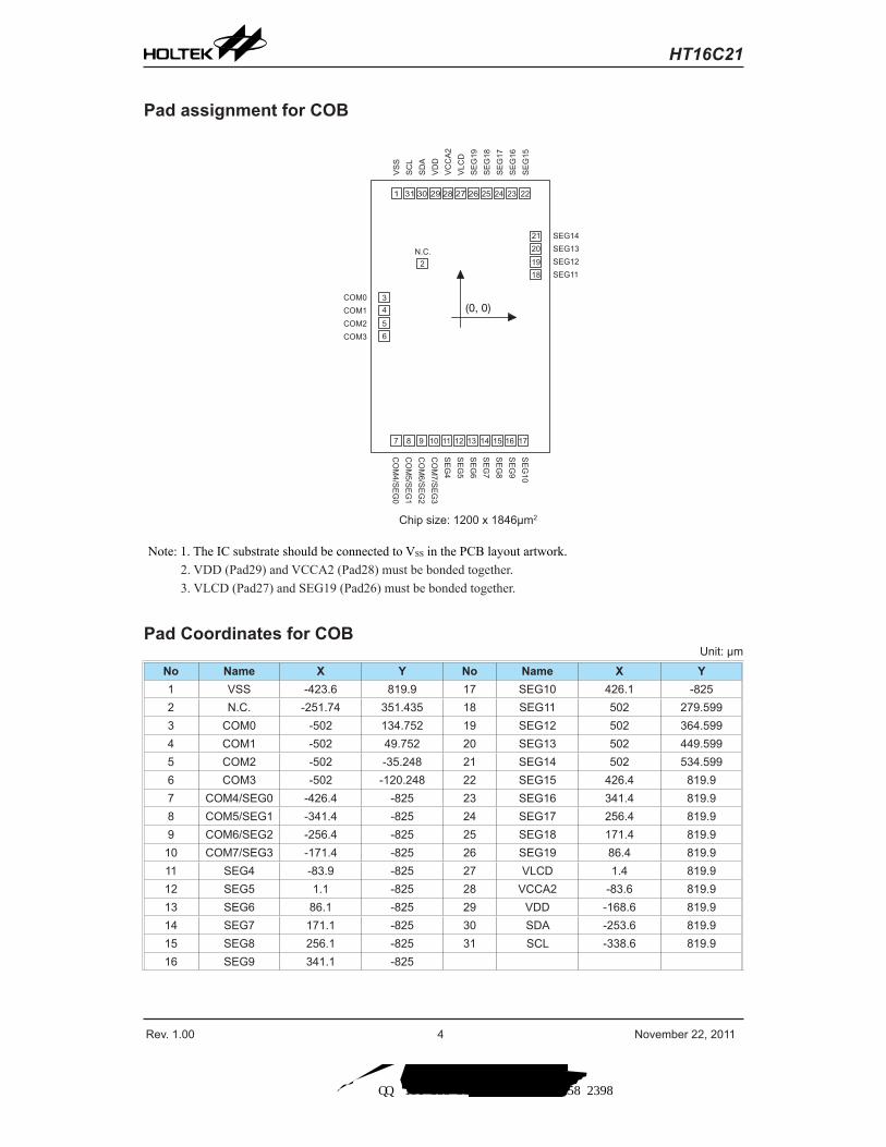
Pad assignment for COB
2N.C.
SE
G10
SE
G9
SE
G8
SE
G7
SE
G6
SE
G5
SE
G4
CO
M7/S
EG
3C
OM
6/SE
G2
CO
M5/S
EG
1C
OM
4/SE
G0
COM0COM1COM2COM3
SEG14SEG13SEG12SEG11
VS
SS
CL
SD
AV
DD
VC
CA
2V
LCD
SE
G19
SE
G18
SE
G17
SE
G16
SE
G15
16 17
1819
2021
222324252627282930311
34
56
(0, 0)
7 8 9 10 11 12 13 14 15
Chip size: 1200 x 1846μm2
Note: 1. The IC substrate should be connected to VSS in the PCB layout artwork.2. VDD (Pad29) and VCCA2 (Pad28) must be bonded together.3. VLCD (Pad27) and SEG19 (Pad26) must be bonded together.
Pad Coordinates for COBUnit: μm
No Name X Y No Name X Y1 VSS -423.6 819.9 17 SEG10 426.1 -8252 N.C. -251.74 351.435 18 SEG11 502 279.5993 COM0 -502 134.752 19 SEG12 502 364.5994 COM1 -502 49.752 20 SEG13 502 449.5995 COM2 -502 -35.248 21 SEG14 502 534.5996 COM3 -502 -120.248 22 SEG15 426.4 819.97 COM4/SEG0 -426.4 -825 23 SEG16 341.4 819.98 COM5/SEG1 -341.4 -825 24 SEG17 256.4 819.99 COM6/SEG2 -256.4 -825 25 SEG18 171.4 819.910 COM7/SEG3 -171.4 -825 26 SEG19 86.4 819.911 SEG4 -83.9 -825 27 VLCD 1.4 819.912 SEG5 1.1 -825 28 VCCA2 -83.6 819.913 SEG6 86.1 -825 29 VDD -168.6 819.914 SEG7 171.1 -825 30 SDA -253.6 819.915 SEG8 256.1 -825 31 SCL -338.6 819.916 SEG9 341.1 -825
索取样品 快速开发 工程服务 技术支持 联系人:许先生 QQ:191 888 5898 TEL:188 9858 2398
Rev. 1.00 5 November 22, 2011
HT16C21
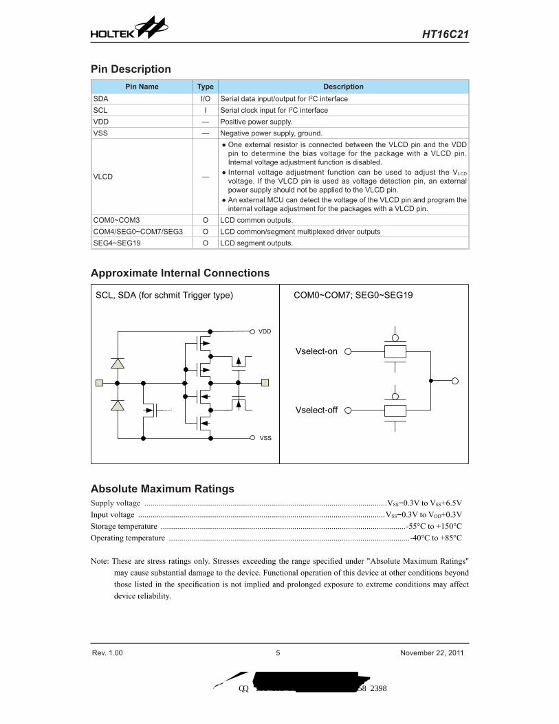
Pin DescriptionPin Name Type Description
SDA I/O Serial data input/output for I2C interfaceSCL I Serial clock input for I2C interfaceVDD — Positive power supply.VSS — Negative power supply, ground.
VLCD —
● One external resistor is connected between the VLCD pin and the VDD pin to determine the bias voltage for the package with a VLCD pin. Internal voltage adjustment function is disabled. ● Internal voltage adjustment function can be used to adjust the VLCD voltage. If the VLCD pin is used as voltage detection pin, an external power supply should not be applied to the VLCD pin. ● An external MCU can detect the voltage of the VLCD pin and program the internal voltage adjustment for the packages with a VLCD pin.
COM0~COM3 O LCD common outputs.COM4/SEG0~COM7/SEG3 O LCD common/segment multiplexed driver outputsSEG4~SEG19 O LCD segment outputs.
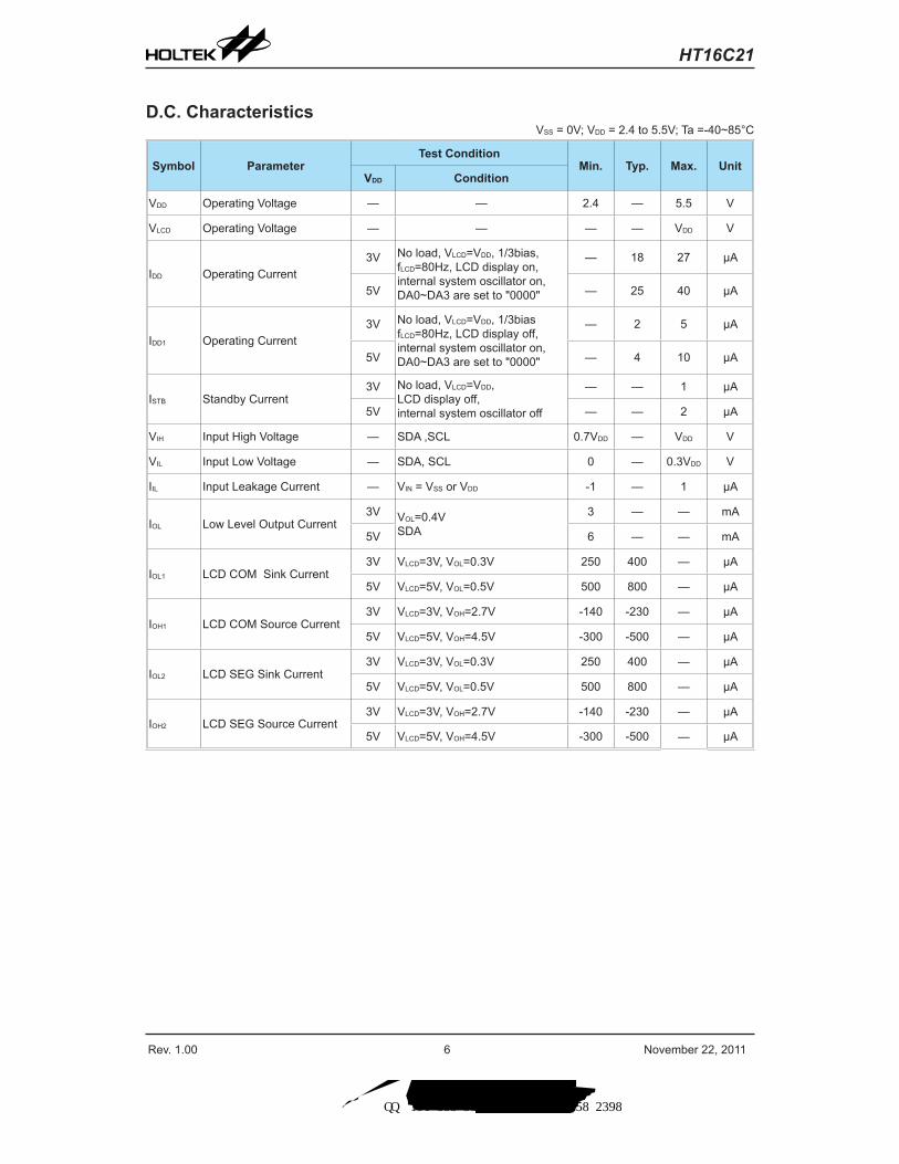
Approximate Internal Connections
VDD
VSS
SCL, SDA (for schmit Trigger type)
Vselect-on
Vselect-off
COM0~COM7; SEG0~SEG19
Absolute Maximum RatingsSupply voltage ......................................................................................................................VSS−0.3V to VSS+6.5V Input voltage ........................................................................................................................VSS−0.3V to VDD+0.3V Storage temperature .......................................................................................................................-55°C to +150°C Operating temperature .....................................................................................................................-40°C to +85°C
Note: These are stress ratings only. Stresses exceeding the range specified under "Absolute Maximum Ratings" may cause substantial damage to the device. Functional operation of this device at other conditions beyond those listed in the specification is not implied and prolonged exposure to extreme conditions may affect device reliability.
索取样品 快速开发 工程服务 技术支持 联系人:许先生 QQ:191 888 5898 TEL:188 9858 2398
Rev. 1.00 6 November 22, 2011
HT16C21
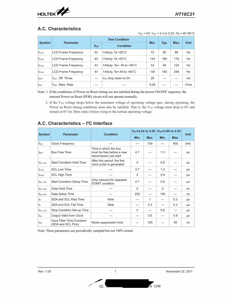
D.C. CharacteristicsVSS = 0V; VDD = 2.4 to 5.5V; Ta =-40~85°C
Symbol ParameterTest Condition
Min. Typ. Max. UnitVDD Condition
VDD Operating Voltage — — 2.4 — 5.5 V
VLCD Operating Voltage — — — — VDD V
IDD Operating Current3V No load, VLCD=VDD, 1/3bias,
fLCD=80Hz, LCD display on, internal system oscillator on,DA0~DA3 are set to "0000"
— 18 27 μA
5V — 25 40 μA
IDD1 Operating Current3V No load, VLCD=VDD, 1/3bias
fLCD=80Hz, LCD display off, internal system oscillator on,DA0~DA3 are set to "0000"
— 2 5 μA
5V — 4 10 μA
ISTB Standby Current3V No load, VLCD=VDD,
LCD display off, internal system oscillator off
— — 1 μA
5V — — 2 μA
VIH Input High Voltage — SDA ,SCL 0.7VDD — VDD V
VIL Input Low Voltage — SDA, SCL 0 — 0.3VDD V
IIL Input Leakage Current — VIN = VSS or VDD -1 — 1 μA
IOL Low Level Output Current3V VOL=0.4V
SDA3 — — mA
5V 6 — — mA
IOL1 LCD COM Sink Current3V VLCD=3V, VOL=0.3V 250 400 — μA
5V VLCD=5V, VOL=0.5V 500 800 — μA
IOH1 LCD COM Source Current3V VLCD=3V, VOH=2.7V -140 -230 — μA
5V VLCD=5V, VOH=4.5V -300 -500 — μA
IOL2 LCD SEG Sink Current3V VLCD=3V, VOL=0.3V 250 400 — μA
5V VLCD=5V, VOL=0.5V 500 800 — μA
IOH2 LCD SEG Source Current3V VLCD=3V, VOH=2.7V -140 -230 — μA
5V VLCD=5V, VOH=4.5V -300 -500 — μA
索取样品 快速开发 工程服务 技术支持 联系人:许先生 QQ:191 888 5898 TEL:188 9858 2398
Rev. 1.00 7 November 22, 2011
HT16C21
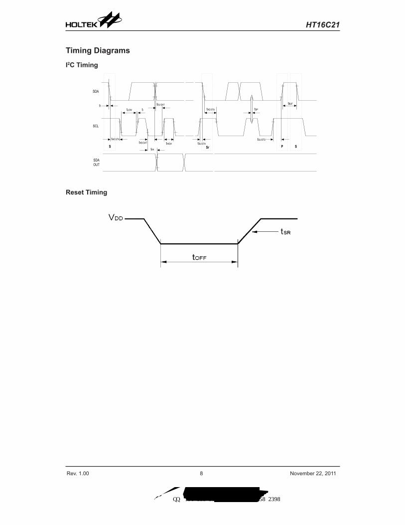
A.C. CharacteristicsVSS = 0V; VDD = 2.4 to 5.5V; Ta =-40~85°C
Symbol ParameterTest Condition
Min. Typ. Max. UnitVDD Condition
fLCD1 LCD Frame Frequency 4V 1/4duty, Ta =25°C 72 80 88 Hz
fLCD2 LCD Frame Frequency 4V 1/4duty, Ta =25°C 144 160 176 Hz
fLCD3 LCD Frame Frequency 4V 1/4duty, Ta=- 40 to +85°C 52 80 124 Hz
fLCD4 LCD Frame Frequency 4V 1/4duty, Ta=-40 to +85°C 104 160 248 Hz
tOFF VDD Off Times — VDD drop down to 0V 20 — — ms
tSR VDD Slew Rate — — 0.05 — — V/ms
Note: 1. If the conditions of Power on Reset timing are not satisfied during the power ON/OFF sequence, the internal Power on Reset (POR) circuit will not operate normally.
2. If the VDD voltage drops below the minimum voltage of operating voltage spec. during operating, the Power on Reset timing conditions must also be satisfied. That is, the VDD voltage must drop to 0V and remain at 0V for 20ms (min.) before rising to the normal operating voltage.
A.C. Characteristics – I2C Interface
Symbol Parameter ConditionVDD=2.4V to 5.5V VDD=3.0V to 5.5V
UnitMin. Max. Min. Max.
fSCL Clock Frequency — — 100 — 400 kHz
tBUF Bus Free TimeTime in which the bus must be free before a new transmission can start
4.7 — 1.3 — μs
tHD: STA Start Condition Hold Time After this period, the firstclock pulse is generated 4 — 0.6 — μs
tLOW SCL Low Time — 4.7 — 1.3 — μs
tHIGH SCL High Time — 4 — 0.6 — μs
tSU: STA Start Condition Setup Time Only relevant for repeated START condition 4.7 — 0.6 — μs
tHD: DAT Data Hold Time — 0 — 0 — ns
tSU: DAT Data Setup Time — 250 — 100 — ns
tR SDA and SCL Rise Time Note — 1 — 0.3 μs
tF SDA and SCL Fall Time Note — 0.3 — 0.3 μs
tSU: STO Stop Condition Set-up Time — 4 — 0.6 — μs
tAA Output Valid from Clock — — 3.5 — 0.9 μs
tSPInput Filter Time Constant (SDA and SCL Pins) Noise suppression time — 100 — 50 ns
Note: These parameters are periodically sampled but not 100% tested.
索取样品 快速开发 工程服务 技术支持 联系人:许先生 QQ:191 888 5898 TEL:188 9858 2398
Rev. 1.00 8 November 22, 2011
HT16C21
Timing Diagrams
I2C Timing
SDA
SCL
tf
tHD:STA
tLOW tr
tHD:DAT
tSU:DAT
tHIGH tSU:STA
tHD:STA
S Sr
tSP
tSU:STO
P
tBUF
StAA
SDAOUT
Reset Timing
索取样品 快速开发 工程服务 技术支持 联系人:许先生 QQ:191 888 5898 TEL:188 9858 2398
Rev. 1.00 9 November 22, 2011
HT16C21
Functional Description
Power-On ResetWhen the power is applied, the device is initialized by an internal power-on reset circuit. The status of the internal circuits after initialization is as follows:
● All common/segment outputs are set to VLCD. ● The drive mode 1/4 duty output and 1/3 bias is selected. ● The System Oscillator and the LCD bias generator are off state. ● LCD Display is off state. ● Internal voltage adjustment function is enabled. ● The Segment / VLCD shared pin is set as the Segment pin. ● Detection switch for the VLCD pin is disabled. ● Frame Frequency is set to 80Hz. ● Blinking function is switched off.
Data transfers on the I2C interface should be avoided for 1 ms following power-on to allow completion of the reset action.
Display Memory – RAM StructureThe display RAM is static 16 x 8-bits RAM which stores the LCD data. Logic “1” in the RAM bit-map indicates the “on” state of the corresponding LCD segment; similarly, logic 0 indicates the ‘off’ state.
The contents of the RAM data are directly mapped to the LCD data. The first RAM column corresponds to the segments operated with respect to COM0. In multiplexed LCD applications the segment data of the second, third and fourth column of the display RAM are time-multiplexed with COM1, COM2 and COM3 respectively. The following is a mapping from the RAM data to the LCD pattern:
Output COM3 COM2 COM1 COM0 Output COM3 COM2 COM1 COM0 AddressSEG1 SEG0 00HSEG3 SEG2 01HSEG5 SEG4 02HSEG7 SEG6 03HSEG9 SEG8 04HSEG11 SEG10 05HSEG13 SEG12 06HSEG15 SEG14 07HSEG17 SEG16 08HSEG19 SEG18 09H
D7 D6 D5 D4 D3 D2 D1 D0 Data
RAM mapping of 20x4 display mode
索取样品 快速开发 工程服务 技术支持 联系人:许先生 QQ:191 888 5898 TEL:188 9858 2398
Rev. 1.00 10 November 22, 2011
HT16C21
Output COM7/SEG3
COM6/SEG2
COM5/SEG1
COM4/SEG0 COM3 COM2 COM1 COM0 address
SEG4 00HSEG5 01HSEG6 02HSEG7 03HSEG8 04HSEG9 05HSEG10 06HSEG11 07HSEG12 08HSEG13 09HSEG14 0AHSEG15 0BHSEG16 0CHSEG17 0DHSEG18 0EHSEG19 0FH
D7 D6 D5 D4 D3 D2 D1 D0 Data
RAM mapping of 16x8 display mode
D0
MSB LSBD1D2D3D4D5D6D7LCD
LED0LED1LED2LED3LED4LED5LED6LED7LED
Display data transfer format for I2C interface
System OscillatorThe timing for the internal logic and the LCD drive signals are generated by an internal oscillator. The System Clock frequency (fSYS) determines the LCD frame frequency. During initial system power on the System Oscillator will be in the stop state.
LCD Bias GeneratorThe full-scale LCD voltage (VOP) is obtained from (VLCD – VSS). The LCD voltage may be temperature compensated externally through the Voltage supply to the VLCD pin.
Fractional LCD biasing voltages, known as 1/3 or 1/4 bias voltage, are obtained from an internal voltage divider of four series resistors connected between VLCD and VSS. The centre resistor can be switched out of circuits to provide a 1/3bias voltage level configuration.
索取样品 快速开发 工程服务 技术支持 联系人:许先生 QQ:191 888 5898 TEL:188 9858 2398
Rev. 1.00 11 November 22, 2011
HT16C21
LCD Drive Mode Waveforms ● When the LCD drive mode is selected as 1/4 duty and 1/3 bias, the waveform and LCD display is shown as
follows:
State1(on)
State1(on)
SEG n+2SEG n+2
SEG nSEG n
COM0COM0
COM1COM1
State2(off)
State2(off)
LCD segmentLCD segment
COM2COM2
VLCDVLCD
VSSVSS
VLCD- Vop/3VLCD- Vop/3
VLCD- 2Vop/3VLCD- 2Vop/3SEG n+3
SEG n+3
COM3COM3
SEG n+1SEG n+1
VLCDVLCD
VSSVSS
VLCD- Vop/3VLCD- Vop/3
VLCD- 2Vop/3VLCD- 2Vop/3
VLCDVLCD
VSSVSS
VLCD- Vop/3VLCD- Vop/3
VLCD- 2Vop/3VLCD- 2Vop/3
VLCDVLCD
VSSVSS
VLCD- Vop/3VLCD- Vop/3
VLCD- 2Vop/3VLCD- 2Vop/3
VLCDVLCD
VSSVSS
VLCD- Vop/3VLCD- Vop/3
VLCD- 2Vop/3VLCD- 2Vop/3
VLCDVLCD
VSSVSS
VLCD- Vop/3VLCD- Vop/3
VLCD- 2Vop/3VLCD- 2Vop/3
VLCDVLCD
VSSVSS
VLCD- Vop/3VLCD- Vop/3
VLCD- 2Vop/3VLCD- 2Vop/3
VLCDVLCD
VSSVSS
VLCD- Vop/3VLCD- Vop/3
VLCD- 2Vop/3VLCD- 2Vop/3
tLCD
Waveforms for 1/4 duty drive mode with 1/3 bias (VOP = VLCD-VSS)
Note: tLCD = 1/fLCD
索取样品 快速开发 工程服务 技术支持 联系人:许先生 QQ:191 888 5898 TEL:188 9858 2398
Rev. 1.00 12 November 22, 2011
HT16C21
● When the LCD drive mode is selected as 1/8 duty and 1/4bias, the waveform and LCD display is shown as follows:
COM0COM0
State1(on)
State1(on)
State2(off)
State2(off)
LCD segmentLCD segmenttLCD
VLCDVLCD
VSSVSS
VLCD- Vop/4VLCD- Vop/4
VLCD- 2Vop/4VLCD- 2Vop/4
VLCD- 3Vop/4VLCD- 3Vop/4
COM1COM1
VLCDVLCD
VSSVSS
VLCD- Vop/4VLCD- Vop/4
VLCD- 2Vop/4VLCD- 2Vop/4
VLCD- 3Vop/4VLCD- 3Vop/4
COM2COM2
VLCDVLCD
VSSVSS
VLCD- Vop/4VLCD- Vop/4
VLCD- 2Vop/4VLCD- 2Vop/4
VLCD- 3Vop/4VLCD- 3Vop/4
COM3COM3
VLCDVLCD
VSSVSS
VLCD- Vop/4VLCD- Vop/4
VLCD- 2Vop/4VLCD- 2Vop/4
VLCD- 3Vop/4VLCD- 3Vop/4
COM4COM4
VLCDVLCD
VSSVSS
VLCD- Vop/4VLCD- Vop/4
VLCD- 2Vop/4VLCD- 2Vop/4
VLCD- 3Vop/4VLCD- 3Vop/4
COM5COM5
VLCDVLCD
VSSVSS
VLCD- Vop/4VLCD- Vop/4
VLCD- 2Vop/4VLCD- 2Vop/4
VLCD- 3Vop/4VLCD- 3Vop/4
COM6COM6
VLCDVLCD
VSSVSS
VLCD- Vop/4VLCD- Vop/4
VLCD- 2Vop/4VLCD- 2Vop/4
VLCD- 3Vop/4VLCD- 3Vop/4
COM7COM7
VLCDVLCD
VSSVSS
VLCD- Vop/4VLCD- Vop/4
VLCD- 2Vop/4VLCD- 2Vop/4
VLCD- 3Vop/4VLCD- 3Vop/4
VLCDVLCD
VSSVSS
VLCD- Vop/4VLCD- Vop/4
VLCD- 2Vop/4VLCD- 2Vop/4
VLCD- 3Vop/4VLCD- 3Vop/4
SEG nSEG n
VLCDVLCD
VSSVSS
VLCD- Vop/4VLCD- Vop/4
VLCD- 2Vop/4VLCD- 2Vop/4
VLCD- 3Vop/4VLCD- 3Vop/4
SEG n+1SEG n+1
VSSVSS
VLCD- Vop/4VLCD- Vop/4
VLCD- 2Vop/4VLCD- 2Vop/4
VLCD- 3Vop/4VLCD- 3Vop/4
SEG n+2SEG n+2
VLCDVLCD
VSSVSS
VLCD- Vop/4VLCD- Vop/4
VLCD- 2Vop/4VLCD- 2Vop/4
VLCD- 3Vop/4VLCD- 3Vop/4
SEG n+3SEG n+3
VLCDVLCD
Waveforms for 1/8 duty drive mode with1/4 bias (VOP = VLCD−VSS)
Note: tLCD = 1/fLCD
索取样品 快速开发 工程服务 技术支持 联系人:许先生 QQ:191 888 5898 TEL:188 9858 2398
Rev. 1.00 13 November 22, 2011
HT16C21
Segment Driver OutputsThe LCD drive section includes 20 segment outputs SEG0 ~ SEG19 or 16 segment outputs SEG4 ~ SEG19 which should be connected directly to the LCD panel. The segment output signals are generated in accordance with the multiplexed column signals and with the data resident in the display latch. The unused segment outputs should be left open-circuit when less than 20 or 16 segment outputs are required.
Column Driver OutputsThe LCD drive section includes 4 column outputs COM0~COM3 or 8 column outputs COM0~COM7 which should be connected directly to the LCD panel. The column output signals are generated in accordance with the selected LCD drive mode. The unused column outputs should be left open-circuit if less than 4 or 8 column outputs are required.
Address PointerThe addressing mechanism for the display RAM is implemented using the address pointer. This allows the loading of an individual display data byte, or a series of display data bytes, into any location of the display RAM. The sequence commences with the initialization of the address pointer by the Address pointer command.
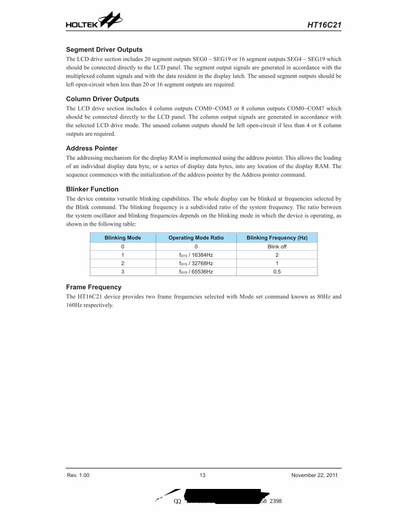
Blinker Function The device contains versatile blinking capabilities. The whole display can be blinked at frequencies selected by the Blink command. The blinking frequency is a subdivided ratio of the system frequency. The ratio between the system oscillator and blinking frequencies depends on the blinking mode in which the device is operating, as shown in the following table:
Blinking Mode Operating Mode Ratio Blinking Frequency (Hz)0 0 Blink off1 fSYS / 16384Hz 22 fSYS / 32768Hz 13 fSYS / 65536Hz 0.5
Frame FrequencyThe HT16C21 device provides two frame frequencies selected with Mode set command known as 80Hz and 160Hz respectively.
索取样品 快速开发 工程服务 技术支持 联系人:许先生 QQ:191 888 5898 TEL:188 9858 2398
Rev. 1.00 14 November 22, 2011
HT16C21
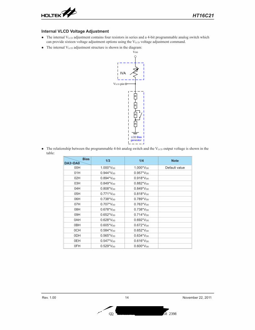
Internal VLCD Voltage Adjustment ● The internal VLCD adjustment contains four resistors in series and a 4-bit programmable analog switch which
can provide sixteen voltage adjustment options using the VLCD voltage adjustment command. ● The internal VLCD adjustment structure is shown in the diagram:
R
LCD Bias generator
VLCD pin
R
R
R
IVA
VDD
● The relationship between the programmable 4-bit analog switch and the VLCD output voltage is shown in the table:
DA3~DA0 Bias 1/3 1/4 Note
00H 1.000*VDD 1.000*VDD Default value01H 0.944*VDD 0.957*VDD
02H 0.894*VDD 0.918*VDD
03H 0.849*VDD 0.882*VDD
04H 0.808*VDD 0.849*VDD
05H 0.771*VDD 0.818*VDD
06H 0.738*VDD 0.789*VDD
07H 0.707*VDD 0.763*VDD
08H 0.678*VDD 0.738*VDD
09H 0.652*VDD 0.714*VDD
0AH 0.628*VDD 0.692*VDD
0BH 0.605*VDD 0.672*VDD
0CH 0.584*VDD 0.652*VDD
0DH 0.565*VDD 0.634*VDD
0EH 0.547*VDD 0.616*VDD
0FH 0.529*VDD 0.600*VDD
索取样品 快速开发 工程服务 技术支持 联系人:许先生 QQ:191 888 5898 TEL:188 9858 2398
Rev. 1.00 15 November 22, 2011
HT16C21
I2C Serial Interface
I2C OperationThe device supports I2C serial interface. The I2C interface is for bidirectional, two-line communication between different ICs or modules. The two lines are a serial data line, SDA, and a serial clock line, SCL. Both lines are connected to the positive supply via pull-up resistors with a typical value of 4.7KΩ. When the I2C interface is free, both lines are high. Devices connected to the I2C interface must have open-drain or open-collector outputs to implement a wired-or function. Data transfer is initiated only when the I2C interface is not busy.
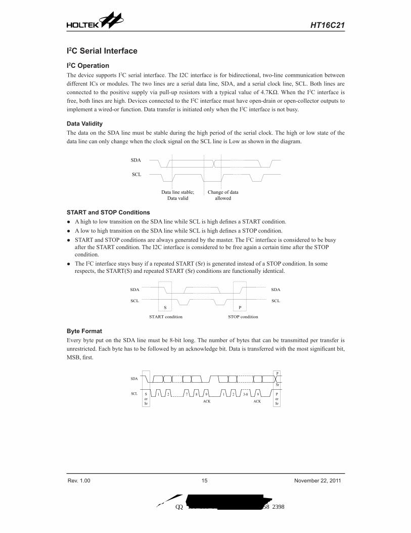
Data ValidityThe data on the SDA line must be stable during the high period of the serial clock. The high or low state of the data line can only change when the clock signal on the SCL line is Low as shown in the diagram.
SDA
SCL
Data line stable;Data valid
Change of data allowed
START and STOP Conditions ● A high to low transition on the SDA line while SCL is high defines a START condition. ● A low to high transition on the SDA line while SCL is high defines a STOP condition. ● START and STOP conditions are always generated by the master. The I2C interface is considered to be busy
after the START condition. The I2C interface is considered to be free again a certain time after the STOP condition.
● The I2C interface stays busy if a repeated START (Sr) is generated instead of a STOP condition. In some respects, the START(S) and repeated START (Sr) conditions are functionally identical.
PS
SDA
SCL
SDA
SCL
START condition STOP condition
Byte FormatEvery byte put on the SDA line must be 8-bit long. The number of bytes that can be transmitted per transfer is unrestricted. Each byte has to be followed by an acknowledge bit. Data is transferred with the most significant bit, MSB, first.
SorSr
PorSr
SDA
SCL 1 2 7 8 9
ACK
1 2 3-8 9
ACK
P
Sr
索取样品 快速开发 工程服务 技术支持 联系人:许先生 QQ:191 888 5898 TEL:188 9858 2398
Rev. 1.00 16 November 22, 2011
HT16C21
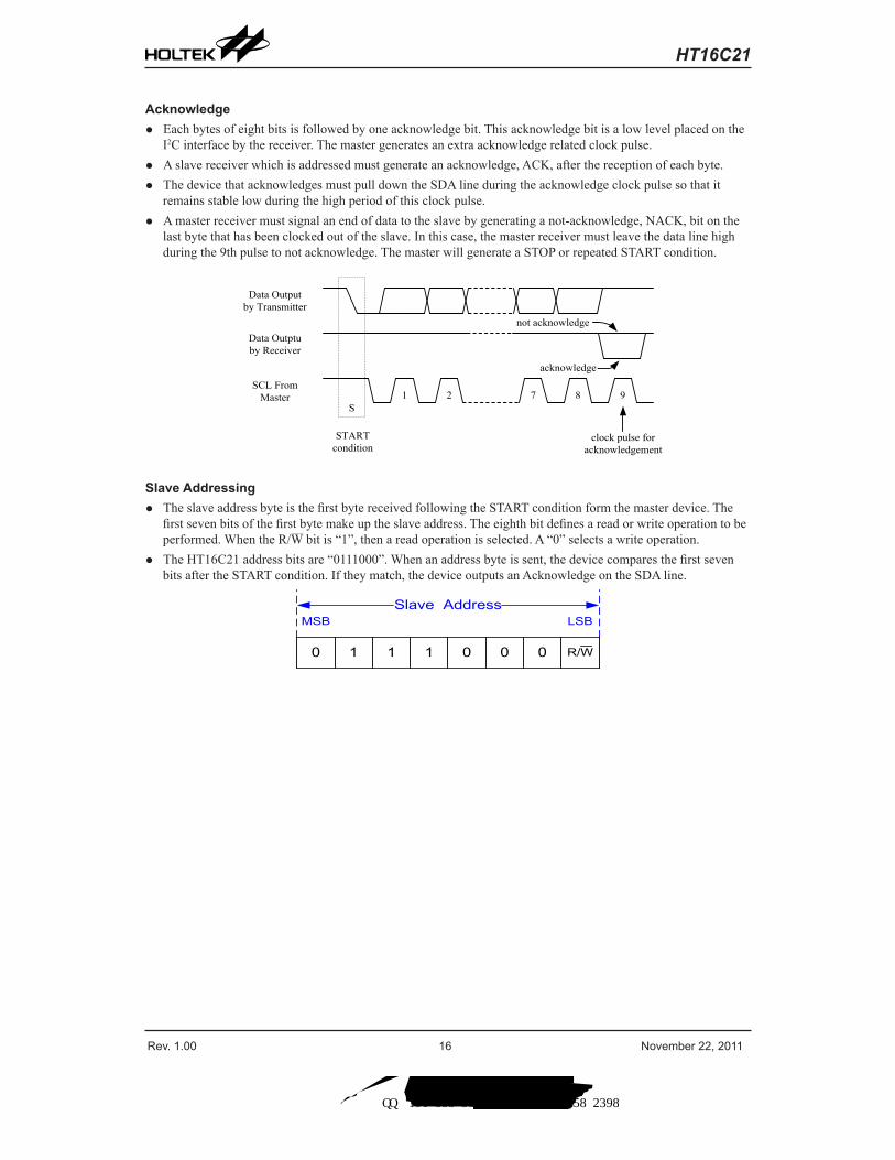
Acknowledge ● Each bytes of eight bits is followed by one acknowledge bit. This acknowledge bit is a low level placed on the
I2C interface by the receiver. The master generates an extra acknowledge related clock pulse. ● A slave receiver which is addressed must generate an acknowledge, ACK, after the reception of each byte. ● The device that acknowledges must pull down the SDA line during the acknowledge clock pulse so that it
remains stable low during the high period of this clock pulse. ● A master receiver must signal an end of data to the slave by generating a not-acknowledge, NACK, bit on the
last byte that has been clocked out of the slave. In this case, the master receiver must leave the data line high during the 9th pulse to not acknowledge. The master will generate a STOP or repeated START condition.
S1 2 7 8 9
clock pulse foracknowledgement
Data Outputby Transmitter
Data Outptuby Receiver
SCL FromMaster
acknowledge
not acknowledge
STARTcondition
Slave Addressing ● The slave address byte is the first byte received following the START condition form the master device. The
first seven bits of the first byte make up the slave address. The eighth bit defines a read or write operation to be performed. When the R/W bit is “1”, then a read operation is selected. A “0” selects a write operation.
● The HT16C21 address bits are “0111000”. When an address byte is sent, the device compares the first seven bits after the START condition. If they match, the device outputs an Acknowledge on the SDA line.
Slave Address
0 1 1 1 0 0 0 R/W
MSB LSB
索取样品 快速开发 工程服务 技术支持 联系人:许先生 QQ:191 888 5898 TEL:188 9858 2398
Rev. 1.00 17 November 22, 2011
HT16C21
Write Operation
Byte Writes Operation ● Command Byte
A Command Byte write operation requires a START condition, a slave address with an R/W bit, a command byte, a command setting byte and a STOP condition for a command byte write operation.
Slave Address
ACKWrite
Command byte
ACK
S 0 1 1 1 0 0 0 0
1st
BIT0BIT1BIT2BIT3BIT4BIT5BIT6BIT7
Command setting
ACK
P
2nd
BIT0BIT1BIT2BIT3BIT4BIT5BIT6BIT7
Command Byte Write Operation
● Display RAM Single Data ByteA display RAM data byte write operation requires a START condition, a slave address with an R/W bit, a command byte, a valid Register Address byte, a Data byte and a STOP condition.
Slave Address
ACKWrite
Command byte
ACK
S 0 1 1 1 0 0 0 0
Data byte
ACK
PD7 D6 D5 D4 D3 D2 D1 D0
Register Address byte
ACK2nd1st
BIT0BIT1BIT2BIT3BIT4BIT5BIT6BIT7 BIT0BIT1BIT2BIT3BIT4BIT5BIT6BIT7
Display RAM Single Data Byte Write Operation
Display RAM Page Write OperationAfter a START condition the slave address with the R/W bit is placed on the I2C interface followed with a command byte and the specified display RAM Register Address of which the contents are written to the internal address pointer. The data to be written to the memory will be transmitted next and then the internal address pointer will be incremented by 1 to indicate the next memory address location after the reception of an acknowledge clock pulse. After the internal address point reaches the maximum memory address, which is 09H for 1/4 duty drive mode or 0FH for 1/8 duty drive mode, the address pointer will be reset to 00H.
Slave Address
ACKWrite
ACK
S 0 1 1 1 0 0 0 0
ACK
2nd
ACK
Data byte
PD7 D6 D5 D4 D3 D2 D1 D0
Nth data
Data byte
D7 D6 D5 D4 D3 D2 D1 D0
2nd data
ACK ACK
Data byte
D7 D6 D5 D4 D3 D2 D1 D0
1st data
ACK
Register Address byteCommand byte
1st
BIT0BIT1BIT2BIT3BIT4BIT5BIT6BIT7 BIT0BIT1BIT2BIT3BIT4BIT5BIT6BIT7
N Bytes Display RAM Data Write Operation
索取样品 快速开发 工程服务 技术支持 联系人:许先生 QQ:191 888 5898 TEL:188 9858 2398
Rev. 1.00 18 November 22, 2011
HT16C21
Display RAM Read Operation ● In this mode, the master reads the HT16C21 data after setting the slave address. Following the R/W bit (=’0”)
is an acknowledge bit, a command byte and the register address byte which is written to the internal address pointer. After the start address of the Read Operation has been configured, another START condition and the slave address transferred on the I2C interface followed by the R/W bit (=’1”). Then the MSB of the data which was addressed is transmitted first on the I2C interface. The address pointer is only incremented by 1 after the reception of an acknowledge clock. That means that if the device is configured to transmit the data at the address of AN+1, the master will read and acknowledge the transferred new data byte and the address pointer is incremented to AN+2. After the internal address pointer reaches the maximum memory address, which is 09H for 1/4 duty drive mode or 0FH for 1/8 duty drive mode, the address pointer will be reset to 00H.
● This cycle of reading consecutive addresses will continue until the master sends a STOP condition.
ACKWrite
ACK
P
Slave Address
S 0 1 1 1 0 0 0 0
Data byte
NACK
D7 D6 D5 D4 D3 D2 D1 D0
1st data
Data byte
ACK
PD7 D6 D5 D4 D3 D2 D1 D0
Nth data
Data byte
D7 D6 D5 D4 D3 D2 D1 D0
2nd data
ACK ACK
ACK
Device Address
Read
S 0 1 1 1 0 0 0 1
ACK
Register Address byteCommand byte
1st 2nd
BIT0BIT1BIT2BIT3BIT4BIT5BIT6BIT7BIT0BIT1BIT2BIT3BIT4BIT5BIT6BIT7
索取样品 快速开发 工程服务 技术支持 联系人:许先生 QQ:191 888 5898 TEL:188 9858 2398
Rev. 1.00 19 November 22, 2011
HT16C21
Command Summary
Display Data Input CommandThis command sends data from MCU to memory MAP of the HT16C21 device.
Function Byte (MSB)Bit7 Bit6 Bit5 Bit4 Bit3 Bit2 Bit1 (LSB)
Bit0 Note R/W Def
Display data input/output command 1st 1 0 0 0 0 0 0 0 W
Address pointer 2nd X X X X A3 A2 A1 A0
Display data start address of memory map
W 00H
Note: ● Power on status: The address is set to 00H. ● If the programmed command is not defined, the function will not be affected. ● For 1/4 duty drive mode after reaching the memory location 09H, the pointer will reset to 00H. ● For 1/8 duty drive mode after reaching the memory location 0FH, the pointer will reset to 00H.
Drive Mode Command
Function Byte (MSB)Bit7 Bit6 Bit5 Bit4 Bit3 Bit2 Bit1 (LSB)
Bit0 Note R/W Def
Driver mode setting command 1st 1 0 0 0 0 0 1 0 W
Duty and bias setting 2nd X X X X X X Duty Bias W 00HNote:
BitDuty Bias
Duty Bias0 0 1/4duty 1/3bias0 1 1/4duty 1/4bias1 0 1/8duty 1/3bias1 1 1/8duty 1/4bias
● Power on status: The drive mode 1/4 duty output and 1/3 bias is selected. ● If the programmed command is not defined, the function will not be affected.
System Mode Command
Function Byte (MSB)Bit7 Bit6 Bit5 Bit4 Bit3 Bit2 Bit1 (LSB)
Bit0 Note R/W Def
System mode setting command 1st 1 0 0 0 0 1 0 0 W
System oscillator and display on/off setting 2nd X X X X X X S E W 00H
Note:Bit
Internal System Oscillator LCD DisplayS E0 X off off1 0 on off1 1 on on
● Power on status: Display off and disable the internal system oscillator. ● If the programmed command is not defined, the function will not be affected.
索取样品 快速开发 工程服务 技术支持 联系人:许先生 QQ:191 888 5898 TEL:188 9858 2398
Rev. 1.00 20 November 22, 2011
HT16C21
Frame Frequency CommandThis command selects the frame frequency.
Function Byte (MSB)Bit7 Bit6 Bit5 Bit4 Bit3 Bit2 Bit1 (LSB)
Bit0 Note R/W Def
Frame frequency command 1st 1 0 0 0 0 1 1 0 W
Frame frequency setting 2nd X X X X X X X F W 00H
Note:Bit
Frame FrequencyF0 80Hz1 160Hz
● Power on status: Frame frequency is set to 80Hz. ● If the programmed command is not defined, the function will not be affected.
Blinking Frequency CommandThis command defines the blinking frequency of the display modes.
Function Byte (MSB)Bit7 Bit6 Bit5 Bit4 Bit3 Bit2 Bit1 (LSB)
Bit0 Note R/W Def
Blinking Frequen-cy command 1st 1 0 0 0 1 0 0 0 W
Blinking Frequency setting 2nd X X X X X X BK1 BK0 W 00H
Note:Bit
Blinking FrequencyBK1 BK0
0 0 Blinking off0 1 2Hz1 0 1Hz1 1 0.5Hz
● Power on status: Blinking function is switched off. ● If the programmed command is not defined, the function will not be affected.
索取样品 快速开发 工程服务 技术支持 联系人:许先生 QQ:191 888 5898 TEL:188 9858 2398
Rev. 1.00 21 November 22, 2011
HT16C21
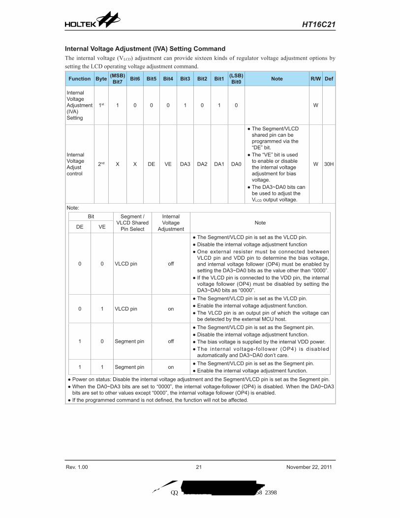
Internal Voltage Adjustment (IVA) Setting CommandThe internal voltage (VLCD) adjustment can provide sixteen kinds of regulator voltage adjustment options by setting the LCD operating voltage adjustment command.
Function Byte (MSB) Bit7 Bit6 Bit5 Bit4 Bit3 Bit2 Bit1 (LSB)
Bit0 Note R/W Def
Internal Voltage Adjustment (IVA) Setting
1st 1 0 0 0 1 0 1 0 W
Internal Voltage Adjust control
2nd X X DE VE DA3 DA2 DA1 DA0
● The Segment/VLCD shared pin can be programmed via the “DE” bit. ● The “VE” bit is used to enable or disable the internal voltage adjustment for bias voltage. ● The DA3~DA0 bits can be used to adjust the VLCD output voltage.
W 30H
Note:Bit Segment /
VLCD Shared Pin Select
Internal Voltage
AdjustmentNote
DE VE
0 0 VLCD pin off
● The Segment/VLCD pin is set as the VLCD pin. ● Disable the internal voltage adjustment function ● One external resister must be connected between VLCD pin and VDD pin to determine the bias voltage, and internal voltage follower (OP4) must be enabled by setting the DA3~DA0 bits as the value other than “0000”. ● If the VLCD pin is connected to the VDD pin, the internal voltage follower (OP4) must be disabled by setting the DA3~DA0 bits as “0000”.
0 1 VLCD pin on
● The Segment/VLCD pin is set as the VLCD pin. ● Enable the internal voltage adjustment function. ● The VLCD pin is an output pin of which the voltage can be detected by the external MCU host.
1 0 Segment pin off
● The Segment/VLCD pin is set as the Segment pin. ● Disable the internal voltage adjustment function. ● The bias voltage is supplied by the internal VDD power. ● The internal voltage-fol lower (OP4) is disabled automatically and DA3~DA0 don’t care.
1 1 Segment pin on ● The Segment/VLCD pin is set as the Segment pin. ● Enable the internal voltage adjustment function.
● Power on status: Disable the internal voltage adjustment and the Segment/VLCD pin is set as the Segment pin. ● When the DA0~DA3 bits are set to “0000”, the internal voltage-follower (OP4) is disabled. When the DA0~DA3 bits are set to other values except “0000”, the internal voltage follower (OP4) is enabled. ● If the programmed command is not defined, the function will not be affected.
索取样品 快速开发 工程服务 技术支持 联系人:许先生 QQ:191 888 5898 TEL:188 9858 2398
Rev. 1.00 22 November 22, 2011
HT16C21
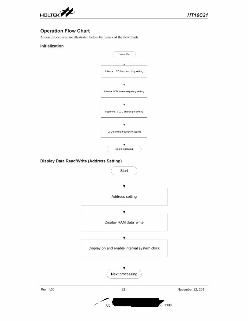
Operation Flow ChartAccess procedures are illustrated below by means of the flowcharts.
Initialization
Power On
Segment / VLCD shared pin setting
Internal LCD frame frequency setting
Internal LCD bias and duty setting
LCD blinking frequency setting
Next processing
Display Data Read/Write (Address Setting)
Start
Next processing
Display RAM data write
Address setting
Display on and enable internal system clock
索取样品 快速开发 工程服务 技术支持 联系人:许先生 QQ:191 888 5898 TEL:188 9858 2398
Rev. 1.00 23 November 22, 2011
HT16C21
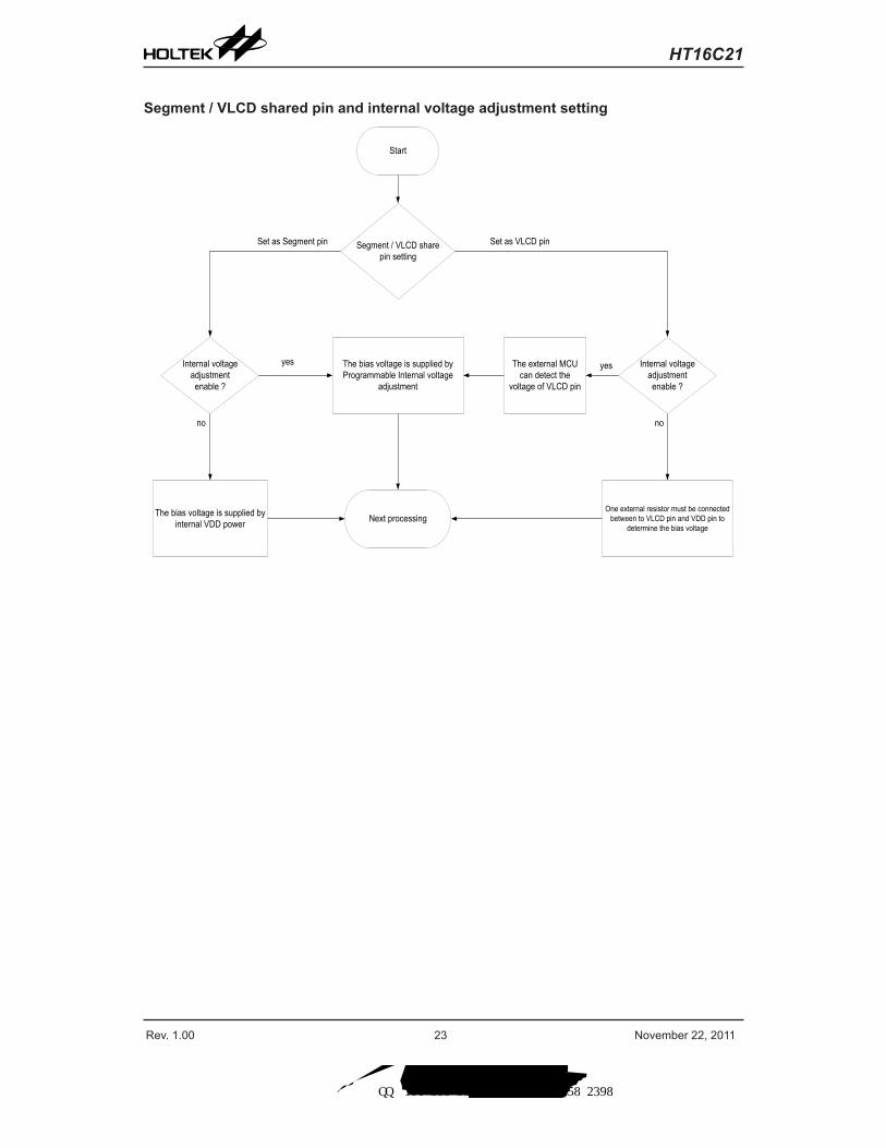
Segment / VLCD shared pin and internal voltage adjustment setting
Segment / VLCD share pin setting
The bias voltage is supplied by Programmable Internal voltage
adjustment
One external resistor must be connected between to VLCD pin and VDD pin to
determine the bias voltage
Internal voltage adjustment enable ?
The external MCU can detect the
voltage of VLCD pin
yes
no
Start
Set as Segment pin
The bias voltage is supplied by internal VDD power Next processing
Set as VLCD pin
Internal voltage adjustment enable ?
no
yes
索取样品 快速开发 工程服务 技术支持 联系人:许先生 QQ:191 888 5898 TEL:188 9858 2398
Rev. 1.00 24 November 22, 2011
HT16C21
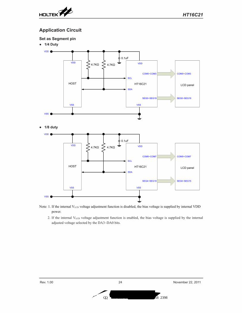
Application Circuit
Set as Segment pin ● 1/4 Duty
LCD panel
COM0~COM3
SEG0~SEG19
COM0~COM3
SEG0~SEG19
SCL
SDA
VDD
VSS
HOST
VDD
VSS
HT16C21
VDD
VSS
0.1uF
4.7KΩ4.7KΩ
● 1/8 duty
LCD panel
COM0~COM7
SEG0~SEG15
COM0~COM7
SEG4~SEG19
SCL
SDA
VDD
VSS
HOST
VDD
VSS
HT16C21
VDD
VSS
0.1uF
4.7KΩ4.7KΩ
Note: 1. If the internal VLCD voltage adjustment function is disabled, the bias voltage is supplied by internal VDD power.
2. If the internal VLCD voltage adjustment function is enabled, the bias voltage is supplied by the internal adjusted voltage selected by the DA3~DA0 bits.
索取样品 快速开发 工程服务 技术支持 联系人:许先生 QQ:191 888 5898 TEL:188 9858 2398
Rev. 1.00 25 November 22, 2011
HT16C21
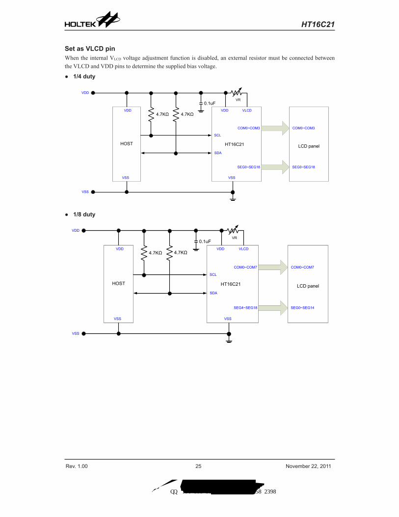
Set as VLCD pinWhen the internal VLCD voltage adjustment function is disabled, an external resistor must be connected between the VLCD and VDD pins to determine the supplied bias voltage.
● 1/4 duty
VR
LCD panel
COM0~COM3
SEG0~SEG18
COM0~COM3
SEG0~SEG18
SCL
SDA
VDD
VSS
HOST
VDD
VSS
HT16C21
VDD
VSS
0.1uFVLCD
4.7KΩ4.7KΩ
● 1/8 duty
VR
LCD panel
COM0~COM7
SEG0~SEG14
COM0~COM7
SEG4~SEG18
SCL
SDA
VDD
VSS
HOST
VDD
VSS
HT16C21
VDD
VSS
0.1uFVLCD
4.7KΩ4.7KΩ
索取样品 快速开发 工程服务 技术支持 联系人:许先生 QQ:191 888 5898 TEL:188 9858 2398
Rev. 1.00 26 November 22, 2011
HT16C21
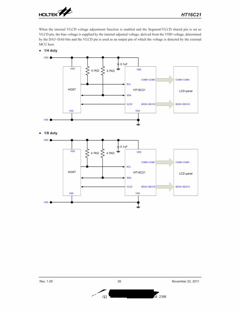
When the internal VLCD voltage adjustment function is enabled and the Segment/VLCD shared pin is set as VLCD pin, the bias voltage is supplied by the internal adjusted voltage, derived from the VDD voltage, determined by the DA3~DA0 bits and the VLCD pin is used as an output pin of which the voltage is detected by the external MCU host.
● 1/4 duty
LCD panel
COM0~COM3
SEG0~SEG18
COM0~COM3
SEG0~SEG18
SCL
SDA
VDD
VSS
HOST
VDD
VSS
HT16C21
VDD
VSS
0.1uF
VLCD
4.7KΩ4.7KΩ
● 1/8 duty
LCD panel
COM0~COM7
SEG0~SEG14
COM0~COM7
SEG4~SEG18
SCL
SDA
VDD
VSS
HOST
VDD
VSS
HT16C21
VDD
VSS
0.1uF
VLCD
4.7KΩ4.7KΩ
索取样品 快速开发 工程服务 技术支持 联系人:许先生 QQ:191 888 5898 TEL:188 9858 2398
Rev. 1.00 27 November 22, 2011
HT16C21
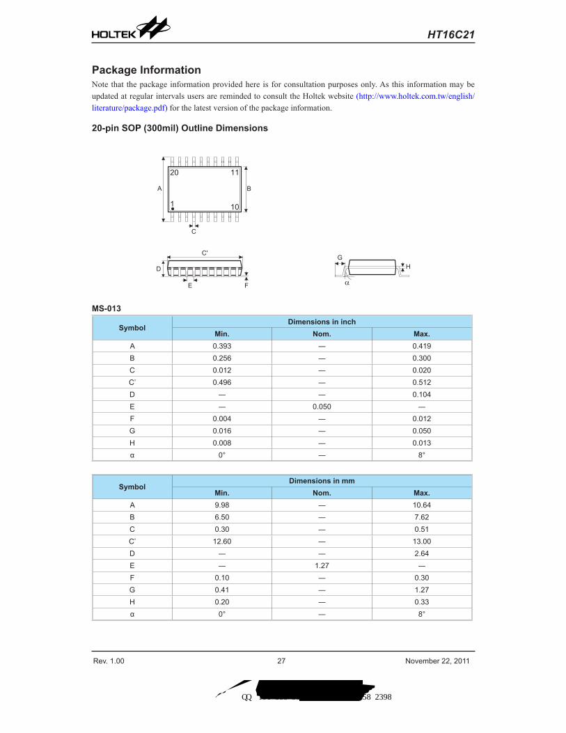
Package InformationNote that the package information provided here is for consultation purposes only. As this information may be updated at regular intervals users are reminded to consult the Holtek website (http://www.holtek.com.tw/english/literature/package.pdf) for the latest version of the package information.
20-pin SOP (300mil) Outline Dimensions
� �
�
� �
� �
� �
�
�
� �
� ��
�
�
MS-013
SymbolDimensions in inch
Min. Nom. Max.A 0.393 ― 0.419B 0.256 ― 0.300C 0.012 ― 0.020C’ 0.496 ― 0.512D ― ― 0.104E ― 0.050 ―F 0.004 ― 0.012G 0.016 ― 0.050H 0.008 ― 0.013α 0° ― 8°
SymbolDimensions in mm
Min. Nom. Max.A 9.98 ― 10.64B 6.50 ― 7.62C 0.30 ― 0.51C’ 12.60 ― 13.00D ― ― 2.64E ― 1.27 ―F 0.10 ― 0.30G 0.41 ― 1.27H 0.20 ― 0.33α 0° ― 8°
索取样品 快速开发 工程服务 技术支持 联系人:许先生 QQ:191 888 5898 TEL:188 9858 2398
Rev. 1.00 28 November 22, 2011
HT16C21
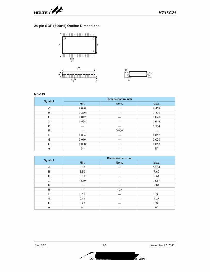
24-pin SOP (300mil) Outline Dimensions
� �
�
� �
� �
� �
�
�
� �
� ��
�
�
MS-013
SymbolDimensions in inch
Min. Nom. Max.A 0.393 ― 0.419B 0.256 ― 0.300C 0.012 ― 0.020C’ 0.598 ― 0.613D ― ― 0.104E ― 0.050 ―F 0.004 ― 0.012G 0.016 ― 0.050H 0.008 ― 0.013α 0° ― 8°
SymbolDimensions in mm
Min. Nom. Max.A 9.98 ― 10.64B 6.50 ― 7.62C 0.30 ― 0.51C’ 15.19 ― 15.57D ― ― 2.64E ― 1.27 ―F 0.10 ― 0.30G 0.41 ― 1.27H 0.20 ― 0.33α 0° ― 8°
索取样品 快速开发 工程服务 技术支持 联系人:许先生 QQ:191 888 5898 TEL:188 9858 2398
Rev. 1.00 29 November 22, 2011
HT16C21
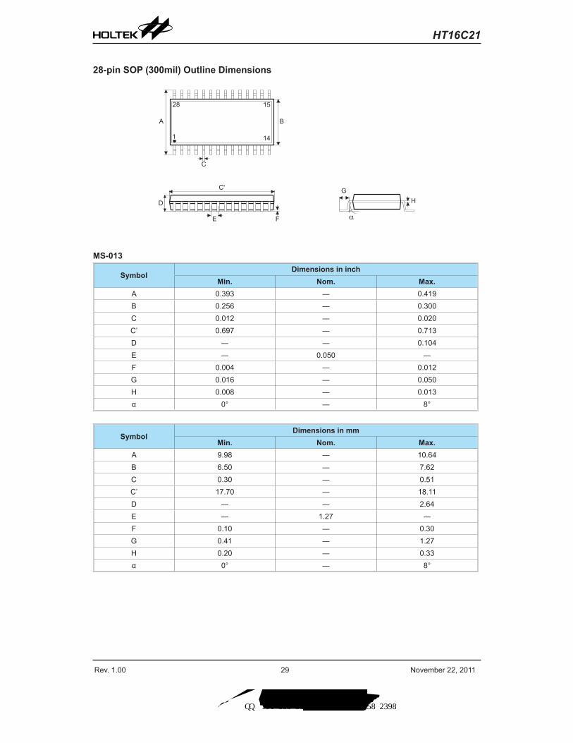
28-pin SOP (300mil) Outline Dimensions
� �
�
� �
� �
� �
�
�
�
� � ��
��
MS-013
SymbolDimensions in inch
Min. Nom. Max.A 0.393 ― 0.419B 0.256 ― 0.300C 0.012 ― 0.020C’ 0.697 ― 0.713D ― ― 0.104E ― 0.050 ―F 0.004 ― 0.012G 0.016 ― 0.050H 0.008 ― 0.013α 0° ― 8°
SymbolDimensions in mm
Min. Nom. Max.A 9.98 ― 10.64B 6.50 ― 7.62C 0.30 ― 0.51C’ 17.70 ― 18.11D ― ― 2.64E ― 1.27 ―F 0.10 ― 0.30G 0.41 ― 1.27H 0.20 ― 0.33α 0° ― 8°
索取样品 快速开发 工程服务 技术支持 联系人:许先生 QQ:191 888 5898 TEL:188 9858 2398
Rev. 1.00 30 November 22, 2011
HT16C21
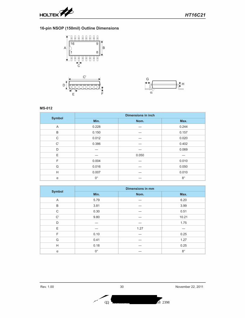
16-pin NSOP (150mil) Outline Dimensions
16-pin NSOP (150mil) Outline Dimensions
� MS-012
SymbolDimensions in inch
Min. Nom. Max.
A 0.228 � 0.244
B 0.150 � 0.157
C 0.012 � 0.020
C� 0.386 � 0.402
D � � 0.069
E � 0.050 �
F 0.004 � 0.010
G 0.016 � 0.050
H 0.007 � 0.010
� 0� � 8�
SymbolDimensions in mm
Min. Nom. Max.
A 5.79 � 6.20
B 3.81 � 3.99
C 0.30 � 0.51
C� 9.80 � 10.21
D � � 1.75
E � 1.27 �
F 0.10 � 0.25
G 0.41 � 1.27
H 0.18 � 0.25
� 0� � 8�
Package Information
1 June 1, 2010
� �
�
�
�
�
� �
�
�
��
�
�
� �
MS-012
SymbolDimensions in inch
Min. Nom. Max.
A 0.228 ― 0.244
B 0.150 ― 0.157
C 0.012 ― 0.020
C' 0.386 ― 0.402
D ― ― 0.069
E ― 0.050 ―
F 0.004 ― 0.010
G 0.016 ― 0.050
H 0.007 ― 0.010
α 0° ― 8°
SymbolDimensions in mm
Min. Nom. Max.
A 5.79 ― 6.20
B 3.81 ― 3.99
C 0.30 ― 0.51
C' 9.80 ― 10.21
D ― ― 1.75
E ― 1.27 ―
F 0.10 ― 0.25
G 0.41 ― 1.27
H 0.18 ― 0.25
α 0° ― 8°
索取样品 快速开发 工程服务 技术支持 联系人:许先生 QQ:191 888 5898 TEL:188 9858 2398
Rev. 1.00 31 November 22, 2011
HT16C21
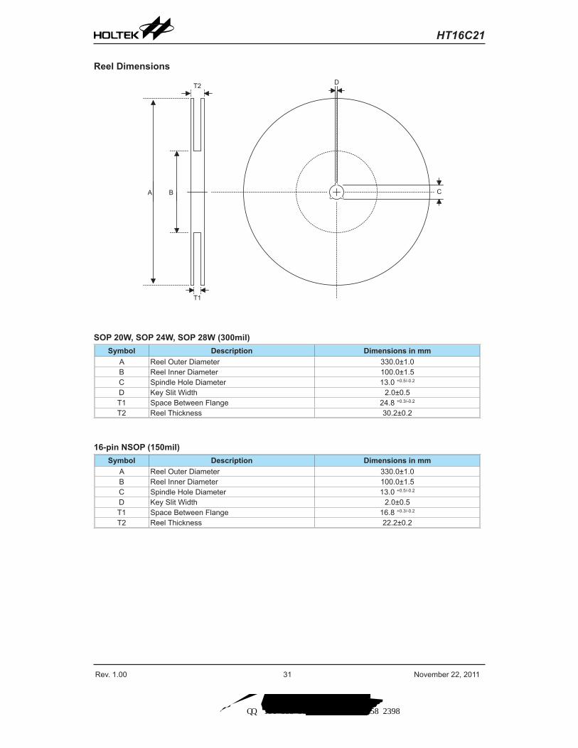
Reel Dimensions
Product Tape and Reel Specifications
Reel Dimensions
SOP 28W (300mil)
Symbol Description Dimensions in mm
A Reel Outer Diameter 330.0�1.0
B Reel Inner Diameter 100.0�1.5
C Spindle Hole Diameter 13.0+0.5/-0.2
D Key Slit Width 2.0�0.5
T1 Space Between Flange 24.8+0.3/-0.2
T2 Reel Thickness 30.2�0.2
Package Information
2 April 1, 2010
� ��
� �
� �
�
SOP 20W, SOP 24W, SOP 28W (300mil)Symbol Description Dimensions in mm
A Reel Outer Diameter 330.0±1.0B Reel Inner Diameter 100.0±1.5C Spindle Hole Diameter 13.0 +0.5/-0.2
D Key Slit Width 2.0±0.5 T1 Space Between Flange 24.8 +0.3/-0.2 T2 Reel Thickness 30.2±0.2
16-pin NSOP (150mil)Symbol Description Dimensions in mm
A Reel Outer Diameter 330.0±1.0B Reel Inner Diameter 100.0±1.5C Spindle Hole Diameter 13.0 +0.5/-0.2
D Key Slit Width 2.0±0.5 T1 Space Between Flange 16.8 +0.3/-0.2 T2 Reel Thickness 22.2±0.2
索取样品 快速开发 工程服务 技术支持 联系人:许先生 QQ:191 888 5898 TEL:188 9858 2398
Rev. 1.00 32 November 22, 2011
HT16C21
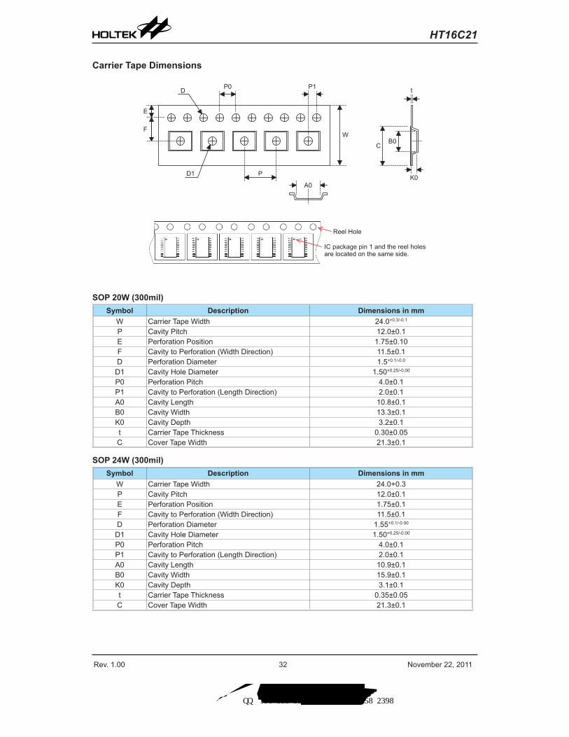
Carrier Tape DimensionsCarrier Tape Dimensions
SOP 28W (300mil)
Symbol Description Dimensions in mm
W Carrier Tape Width 24.0�0.3
P Cavity Pitch 12.0�0.1
E Perforation Position 1.75�0.10
F Cavity to Perforation (Width Direction) 11.5�0.1
D Perforation Diameter 1.5+0.1/-0.0
D1 Cavity Hole Diameter 1.50+0.25/-0.00
P0 Perforation Pitch 4.0�0.1
P1 Cavity to Perforation (Length Direction) 2.0�0.1
A0 Cavity Length 10.85�0.10
B0 Cavity Width 18.34�0.10
K0 Cavity Depth 2.97�0.10
t Carrier Tape Thickness 0.35�0.01
C Cover Tape Width 21.3�0.1
Package Information
3 April 1, 2010
�� �
�
� �� �
�
�
�
�
� �
� �
� �
�
� � � � � � � � � � � � � � � � � � � � � � � � � � � � � � �
� � � � � � � � � � � � � � � � � � � � � � � � � �
� � � � � � � � �
SOP 20W (300mil)Symbol Description Dimensions in mm
W Carrier Tape Width 24.0+0.3/-0.1
P Cavity Pitch 12.0±0.1E Perforation Position 1.75±0.10F Cavity to Perforation (Width Direction) 11.5±0.1D Perforation Diameter 1.5+0.1/-0.0
D1 Cavity Hole Diameter 1.50+0.25/-0.00
P0 Perforation Pitch 4.0±0.1P1 Cavity to Perforation (Length Direction) 2.0±0.1A0 Cavity Length 10.8±0.1B0 Cavity Width 13.3±0.1K0 Cavity Depth 3.2±0.1t Carrier Tape Thickness 0.30±0.05C Cover Tape Width 21.3±0.1
SOP 24W (300mil)Symbol Description Dimensions in mm
W Carrier Tape Width 24.0+0.3
P Cavity Pitch 12.0±0.1E Perforation Position 1.75±0.1F Cavity to Perforation (Width Direction) 11.5±0.1D Perforation Diameter 1.55+0.1/-0.00
D1 Cavity Hole Diameter 1.50+0.25/-0.00
P0 Perforation Pitch 4.0±0.1P1 Cavity to Perforation (Length Direction) 2.0±0.1A0 Cavity Length 10.9±0.1B0 Cavity Width 15.9±0.1K0 Cavity Depth 3.1±0.1t Carrier Tape Thickness 0.35±0.05C Cover Tape Width 21.3±0.1
索取样品 快速开发 工程服务 技术支持 联系人:许先生 QQ:191 888 5898 TEL:188 9858 2398
Rev. 1.00 33 November 22, 2011
HT16C21
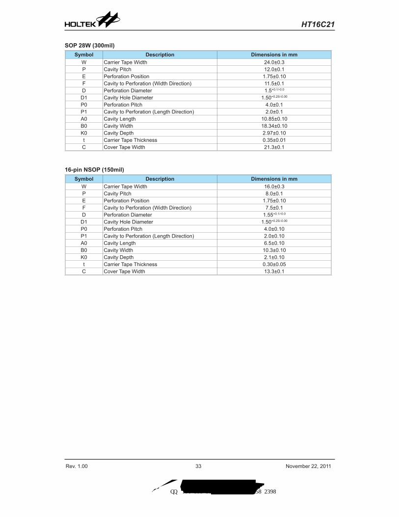
SOP 28W (300mil)Symbol Description Dimensions in mm
W Carrier Tape Width 24.0±0.3P Cavity Pitch 12.0±0.1E Perforation Position 1.75±0.10F Cavity to Perforation (Width Direction) 11.5±0.1D Perforation Diameter 1.5+0.1/-0.0
D1 Cavity Hole Diameter 1.50+0.25/-0.00
P0 Perforation Pitch 4.0±0.1P1 Cavity to Perforation (Length Direction) 2.0±0.1A0 Cavity Length 10.85±0.10B0 Cavity Width 18.34±0.10K0 Cavity Depth 2.97±0.10t Carrier Tape Thickness 0.35±0.01C Cover Tape Width 21.3±0.1
16-pin NSOP (150mil)Symbol Description Dimensions in mm
W Carrier Tape Width 16.0±0.3P Cavity Pitch 8.0±0.1E Perforation Position 1.75±0.10F Cavity to Perforation (Width Direction) 7.5±0.1D Perforation Diameter 1.55+0.1/-0.0
D1 Cavity Hole Diameter 1.50+0.25/-0.00
P0 Perforation Pitch 4.0±0.10P1 Cavity to Perforation (Length Direction) 2.0±0.10A0 Cavity Length 6.5±0.10B0 Cavity Width 10.3±0.10 K0 Cavity Depth 2.1±0.10t Carrier Tape Thickness 0.30±0.05C Cover Tape Width 13.3±0.1
索取样品 快速开发 工程服务 技术支持 联系人:许先生 QQ:191 888 5898 TEL:188 9858 2398
Rev. 1.00 34 November 22, 2011
HT16C21
Holtek Semiconductor Inc. (Headquarters)No.3, Creation Rd. II, Science Park, Hsinchu, TaiwanTel: 886-3-563-1999Fax: 886-3-563-1189http://www.holtek.com.tw
Holtek Semiconductor Inc. (Taipei Sales Office)4F-2, No. 3-2, YuanQu St., Nankang Software Park, Taipei 115, TaiwanTel: 886-2-2655-7070Fax: 886-2-2655-7373Fax: 886-2-2655-7383 (International sales hotline)
Holtek Semiconductor (China) Inc. (Dongguan Sales Office)Building No.10, Xinzhu Court, (No.1 Headquarters), 4 Cuizhu Road, Songshan Lake, Dongguan, China 523808Tel: 86-769-2626-1300Fax: 86-769-2626-1311, 86-769-2626-1322
Holtek Semiconductor (USA), Inc. (North America Sales Office)46729 Fremont Blvd., Fremont, CA 94538, USATel: 1-510-252-9880BFax: 1-510-252-9885http://www.holtek.com
Copyright© 2011 by HOLTEK SEMICONDUCTOR INC.The information appearing in this Data Sheet is believed to be accurate at the time of publication. However, Holtek assumes no responsibility arising from the use of the specifications described. The applications mentioned herein are used solely for the purpose of illustration and Holtek makes no warranty or representation that such applications will be suitable without further modification, nor recommends the use of its products for application that may present a risk to human life due to malfunction or otherwise. Holtek's products are not authorized for use as critical components in life support devices or systems. Holtek reserves the right to alter its products without prior notification. For the most up-to-date information, please visit our web site at http://www.holtek.com.tw.
索取样品 快速开发 工程服务 技术支持 联系人:许先生 QQ:191 888 5898 TEL:188 9858 2398