Embed Size (px)
Citation preview

FN3043Rev 2.00Aug 2000
HS-82C54RHRadiation Hardened CMOS Programmable Interval Timer
DATASHEET
Data Sheet August 2000
The Intersil HS-82C54RH is a high performance, radiation hardened CMOS version of the industry standard 8254 and is manufactured using a hardened field, self-aligned silicon gate CMOS process. It has three independently programmable and functional 16-bit counters, each capable of handling clock input frequencies of up to 5MHz. Six programmable timer modes allow the HS-82C54RH to be used as an event counter, elapsed time indicator, a programmable one-shot, or for any other timing application. The high performance, radiation hardness, and industry standard configuration of the HS-82C54RH make it compatible with the HS-80C86RH radiation hardened microprocessor.
Static CMOS circuit design insures low operating power. The Intersil hardened field CMOS process results in performance equal to or greater than existing radiation resistant products at a fraction of the power.
Specifications for Rad Hard QML devices are controlled by the Defense Supply Center in Columbus (DSCC). The SMD numbers listed here must be used when ordering.
Detailed Electrical Specifications for these devices are contained in SMD 5962-95713. A “hot-link” is provided on our homepage for downloading.www.intersil.com/spacedefense/space.asp
Features
• Electrically Screened to SMD # 5962-95713
• QML Qualified per MIL-PRF-38535 Requirements
• Radiation Performance
- Total Dose. . . . . . . . . . . . . . . . . . . . . 100 krad(Si) (Max)
- Transient Upset . . . . . . . . . . . . . . . . . . . .>108 rad(Si)/s
- Latch Up Free EPI-CMOS
• Low Power Consumption
- IDDSB. . . . . . . . . . . . . . . . . . . . . . . . . . . . . . . . . . .20A
- IDDOP . . . . . . . . . . . . . . . . . . . . . . . . . . . . . . . . . 12mA
• Pin Compatible with NMOS 8254 and the Intersil 82C54
• High Speed, “No Wait State” Operation with 5MHz HS-80C86RH
• Three Independent 16-Bit Counters
• Six Programmable Counter Modes
• Binary or BCD Counting
• Status Read Back Command
• Hardened Field, Self-Aligned, Junction Isolated CMOS Process
• Single 5V Supply
• Military Temperature Range . . . . . . . . . . . -55oC to 125oCOrdering Information
ORDERING NUMBERINTERNAL
MKT. NUMBERTEMP. RANGE
(oC)
5962R9571301QJC HS1-82C54RH-8 -55 to 125
5962R9571301QXC HS9-82C54RH-8 -55 to 125
5962R9571301VJC HS1-82C54RH-Q -55 to 125
FN3043 Rev 2.00 Page 1 of 17Aug 2000

HS-82C54RH
Pinouts24 LEAD CERAMIC DUAL-IN-LINE METAL SEAL PACKAGE
(SBDIP) MIL-STD-1835 CDIP2-T24TOP VIEW
24 LEAD CERAMIC METAL SEAL FLATPACK PACKAGE (FLATPACK) MIL-STD-1835 CDFP4-F24
TOP VIEW
1
2
3
4
5
6
7
8
9
10
11
12
D7
D6
D5
D4
D3
D2
D1
D0
CLK 0
OUT 0
GATE 0
GND
16
17
18
19
20
21
22
23
24
15
14
13
VDD
RD
CS
A1
A0
OUT 2
CLK 1
GATE 1
OUT 1
WR
CLK 2
GATE 2
24
23
22
21
20
19
18
17
16
15
14
13
2
3
4
5
6
7
8
9
10
11
12
1
GND
D7
D6
D5
D4
D3
D2
D1
D0
CLK 0
OUT 0
GATE 0
VDD
OUT1
GATE 1
CLK 1
GATE 2
OUT 2
WR
RD
CS
A1
CLK 2
A0
Pin Descriptions
SYMBOLPIN
NUMBER TYPE DESCRIPTION
D7-D0 1-8 I/O DATA: Bi-directional three state data bus lines, connected to system data bus.
CLK 0 9 I CLOCK 0: Clock input of Counter 0.
OUT 0 10 O OUT 0: Output of Counter 0.
GATE 0 11 I GATE 0: Gate input of Counter 0.
GND 12 GROUND: Power supply connection.
OUT 1 13 O OUT 1: Output of Counter 1.
GATE 1 14 I GATE 1: Gate input of Counter 1.
CLK 1 15 I CLOCK 1: Clock input of Counter 1.
GATE 2 16 I GATE 2: Gate input of Counter 2.
OUT 2 17 O OUT 2: Output of Counter 2.
CLK 2 18 I CLOCK 2: Clock input of Counter 2.
A0, A1 19-20 I ADDRESS: Select inputs for one of the three counters or Control Word Register for read/write operations. Normally connected to the system address bus.
A1 A0 Selects
0 0 Counter 0
0 1 Counter 1
1 0 Counter 2
1 1 Control Word Register
CS 21 I CHIP SELECT: A low on this input enables the HS-82C54RH to respond to RD and WR signals. RD and WR are ignored otherwise.
RD 22 I READ: This input is low during CPU read operations.
WR 23 I WRITE: This input is low during CPU write operations.
VDD 24 VDD: The +5V power supply pin. A 0.1F capacitor between pins 12 and 24 is recommended for decoupling.
FN3043 Rev 2.00 Page 2 of 17Aug 2000

HS-82C54RH
Functional Diagram
AC Test Circuits
NOTE: Includes stray and jig capacitance.
AC Testing Input, Output Waveform
NOTE: AC Testing: All input signals must switch between VIL -0.4V and VIH +0.4V. Input rise and fall times are driven at 1ns/V.
(8)DATABUS
BUFFER
READ/WRITELOGIC
CONTROLWORD
REGISTER
D7-D0
RD
WR
A0A1
CS
INT
ER
NA
L B
US
COUNTER1
COUNTER0
COUNTER2
OUT 1GATE 1CLK 1
OUT 0GATE 0CLK 0
OUT 2GATE 2CLK 2
CONTROLWORD
REGISTER
STATUSLATCH
STATUSREGISTER
CONTROLLOGIC
OUT NGATE N
CLK N
CRM CRL
OLM OLL
CE
INTERNAL BUS
TEST CONDITION DEFINITION TABLE
TEST CONDITION V1 R1 R2 C1
1 1.7V 510 OPEN 150pF
TESTPOINT
OUTPUT FROM DEVICE UNDER TEST
V1
R1
R2 C1 (NOTE)
1.5V 1.5VVIL -0.4V
INPUT
VIH +0.4V
VOL
INPUT
VOH
FN3043 Rev 2.00 Page 3 of 17Aug 2000

HS-82C54RH
Waveforms
FIGURE 1. WRITE FIGURE 2. READ
FIGURE 3. RECOVERY FIGURE 4. CLOCK AND GATE
TWHAX
A0-1
DATA
TWHDX
TWLWH
TDVWH
TAVWL
VALID
WR
CS
TSLWL
BUS
TRHDZ
VALID
TRHAX
TSLRL
TRLDV
A0-1
CS
DATA
RDTRLRH
TAVRL
BUS
RD, WR
TRHRLTWHWL
TCHGX
TCH1CH2TGVCH
TGLOV
TGLGH TCLOV
TGHGL TCHGX
TGVCH
TCL1CL2TCLCL
TCLCHTCHCL
CLK
GATE G
OUTPUT 0
FN3043 Rev 2.00 Page 4 of 17Aug 2000

HS-82C54RH
Burn-In CircuitsSTATIC CONFIGURATION FOR BOTH
FLATPACK AND SBDIP PACKAGE
NOTES:
1. VDD = 6.5V 5%
2. TA = 125oC Minimum
3. Resistors = 10k4. IDD < 100A
5. AC: F0 is compliment of F0F0 is a 50% duty cycle pulse burstF0 is left high after pulse burst
DYNAMIC CONFIGURATION FOR BOTHFLATPACK AND SBDIP PACKAGE
NOTES:
6. VDD = 6.5V 5% (Burn-In)
7. VDD = 6.0V 5% (Life Test)
8. TA = 125oC Minimum
9. IDD < 20mA
10. Resistors = 10kexcept for loads = 2.7k11. -0.3V VIL 0.8V
12. VDD -1.0V VIH VDD +0.5V
13. AC: F0 is compliment of F0F0 = 100kHz 10%, 50% Duty CycleF1 = F0/2, F2 = F1/2 . . . F10 = F9/2
1
2
3
4
5
6
7
8
9
10
11
12
16
17
18
19
20
21
22
24
15
14
13
23
VDD
OPEN
F0
OPEN
OPEN
F0
1
2
3
4
5
6
7
8
9
10
11
12
16
17
18
19
20
21
22
24
15
14
13
23
VDD
LOAD
F2
LOAD
LOAD
F9
F7
F6
F5
F4
F3
F8
F10
F11
F1
F0
F0
VDD
LOAD2.7k
2.7k
Irradiation CircuitsHS-82C54RH
NOTES:
14. VDD = 5.5V 10%, TA = 25oC
15. Group E Testing is performed in Sidebrazed DIP
16. Group E Sample Size is 2 die/wafer
1
2
3
4
5
6
7
8
9
10
11
12
16
17
18
19
20
21
22
23
24
15
14
13
N/C
N/C
5.5V
N/C
5.5V
FN3043 Rev 2.00 Page 5 of 17Aug 2000

HS-82C54RH
Functional Description
General
The HS-82C54RH is a programmable interval timer/counter designed for use with microcomputer systems. It is a general purpose, multi-timing element that can be treated as an array of I/O ports in the system software.
The HS-82C54RH solves one of the most common problems in any microcomputer system, the generation of accurate time delays under software control. Instead of setting up timing loops in software, the programmer configures the HS-82C54RH to match his requirements and programs one of the counters for the desired delay. After the desired delay, the HS-82C54RH will interrupt the CPU. Software overhead is minimal and variable length delays can easily be accommodated.
Some of the other timer functions common to micro-computers which can be implemented with the HS-82C54RH are:
• Real time clock
• Event counter
• Digital one-shot
• Programmable rate generator
• Square wave generator
• Binary rate multiplier
• Complex waveform generator
• Complex motor controller
Data Bus Buffer
This three-state, bi-directional, 8-bit buffer is used to interface the HS-82C54RH to the system bus (see Figure 5).
Read/Write Logic
The Read/Write Logic accepts inputs from the system bus and generates control signals for the other functional blocks of the HS-82C54RH. A1 and A0 select one of the three counters or the Control Word Register to be read from/written into. A “low” on the RD input tells the HS-82C54RH that the CPU is reading one of the counters. A “low” on the WR input tells the HS-82C54RH that the CPU is writing either a Control Word or an initial count. Both RD and WR are qualified by CS; RD and WR are ignored unless the HS-82C54RH has been selected by holding CS low.
Control Word Register
The Control Word Register (Figure 6) is selected by the Read/Write Logic when A1, A0 = 11. If the CPU then does a write operation to the HS-82C54RH, the data is stored in the Control Word Register and is interpreted as a Control Word used to define the Counter operation.
The Control Word Register can only be written to; status information is available with the Read-Back Command.
Counter 0, Counter 1, Counter 2
These three functional clocks are identical in operation, so only a single Counter will be described. The internal block diagram of a single counter is shown in Figure 7. The counters are fully independent. Each Counter may operate in a different Mode.
The Control Word Register is shown in the figure; it is not part of the Counter itself, but its contents determine how the Counter operates.
(8)
CONTROLWORD
REGISTER
D7-D0
RD
WR
A0A1
CS
INT
ER
NA
L B
US
COUNTER1
COUNTER0
COUNTER2
OUT 1GATE 1CLK 1
OUT 0GATE 0CLK 0
OUT 2GATE 2CLK 2
DATABUS
BUFFER
READ/WRITELOGIC
FIGURE 5. DATA BUS BUFFER AND READ/WRITE LOGIC FUNCTION
(8)DATABUS
BUFFER
READ/WRITELOGIC
CONTROLWORD
REGISTER
D7-D0
RD
WR
A0A1
CS
INT
ER
NA
L B
US
COUNTER1
COUNTER0
COUNTER2
OUT 1GATE 1CLK 1
OUT 0GATE 0CLK 0
OUT 2GATE 2CLK 2
FIGURE 6. CONTROL WORD REGISTER AND COUNTER FUNCTIONS
FN3043 Rev 2.00 Page 6 of 17Aug 2000

HS-82C54RH
The Status Register, shown in the figure, when latched, contains the current contents of the Control Word Register and status of the output and null count flag. (See detailed explanation of the Read-Back Command.)
The actual counter is labeled CE for “Counting Element”. It is a 16-bit presettable synchronous down counter.
OLM and OLL are two 8-bit latches. OL stands for “Output Latch”, subscripts M and L for “Most significant byte” and “Least significant byte”, respectively. Both are normally referred to as one unit and called just OL. These latches normally “follow” the CE, but if a suitable Counter Latch Command is sent to the HS-82C54RH, the OL latches the present count until read by the CPU and then returns to “following” the CE. One latch at a time is enabled by the counter’s Control Logic to drive the internal bus. This is how the 16-bit Counter communicates over the 8-bit internal bus. Note that the CE itself cannot be read; whenever you read the count, it is the OL that is being read.
Similarly, there are two 8-bit registers called CRM and CRL (for “Count Register”). Both are normally referred to as one unit and called just CR. When a new count is written to the Counter, the count is stored in the CR and later transferred to the CE. The Control Logic allows one register at a time to be loaded from the internal bus. Both bytes are transferred to the CE simultaneously. CRM and CRL are cleared when the Counter is programmed for one byte counts (either most significant byte only or least significant byte only) the other byte will be zero. Note that the CE cannot be written into; whenever a count is written, it is written into the CR.
The Control Logic is also shown in the diagram. CLKn, GATEn, and OUTn are all connected to the outside world through the Control Logic.
HS-82C54RH System Interface
The HS-82C54RH is treated by the system software as an array of peripheral I/O ports; three are Counters and the fourth is a Control Word Register for MODE programming.
Basically, the select inputs A0, A1 connect to the A0, A1 address bus signals of the CPU. The CS can be derived directly from the address bus using a linear select method or it can be connected to the output of a decoder, such as a Intersil HD-6440 for larger systems.
Operational Description
General
After power-up, the state of the HS-82C54RH is undefined. The Mode, count value, and output of all Counters are undefined.
How each Counter operates is determined when it is programmed. Each Counter must be programmed before it can be used. Unused Counters need not be programmed.
Programming The HS-82C54RH
Counters are programmed by writing a Control Word and then an initial count.
All Control Words are written into the Control Word Register, which is selected when A1, A0 = 11. The Control Word specifies which Counter is being programmed.
By contrast, initial counts are written into the Counters, not the Control Word Register. The A1, A0 inputs are used to select the Counter to be written into. The format of the initial count is determined by the Control Word used.
Write Operations
The programming procedure for the HS-82C54RH is very flexible. Only two conventions need to be remembered:
1. For each Counter, the Control Word must be written before the initial count is written.
2. The initial count must follow the count format specified in the Control Word (least significant byte only, most significant
CONTROLWORD
REGISTER
STATUSLATCH
STATUSREGISTER
CONTROLLOGIC
OUT NGATE N
CLK N
CRM CRL
OLM OLL
CE
INTERNAL BUS
FIGURE 7. COUNTER INTERNAL BLOCK DIAGRAM
DATA BUS (8)
ADDRESS BUS (16)
CONTROL BUS
A1 A0
I/OR I/OW
8
CSA1 A0
COUNTER0
OUT GATE CLK
COUNTER1
OUT GATE CLK
COUNTER2
OUT GATE CLK
D0-D7 RD WRHS-82C54RH
FIGURE 8. HS-82C54RH SYSTEM INTERFACE
FN3043 Rev 2.00 Page 7 of 17Aug 2000

HS-82C54RH
byte only, or least significant byte and then most significant byte).
Since the Control Word Register and the three Counter shave separate addresses (selected by the A1, A0 inputs), and each
Control Word specifies the Counter it applies to (SC0, SC1 bits), no special instruction sequence is required. Any programming sequence that follows the conventions above is acceptable.
Control Word Format
A1, A0 = 11; CS = 0; RD = 1; WR = 0
D7 D6 D5 D4 D3 D2 D1 D0
SC1 SC2 RW1 RW0 M2 M1 M0 BCD
SC - SELECT COUNTER: M - MODE:
SC1 SC0 M2 M1 M0
0 0 Select Counter 0 0 0 0 Mode 0
0 1 Select Counter 1 0 0 1 Mode 1
1 0 Select Counter 2 X 1 0 Mode 2
1 1 Read-Back Command (See Read Operations)
X 1 1 Mode 3
RW - READ/WRITE 1 0 0 Mode 4
RW1 RW0 1 0 1 Mode 5
0 0 Counter Latch Command (See Read Operations)
BCD - BINARY CODED DECIMAL:
0 1 Read/Write least significant byte only. 0 Binary Counter 16-bits
1 0 Read/Write most significant byte only. 1 Binary Coded Decimal (BCD) Counter (4 Decades)
1 1 Read/Write least significant byte first, then most significant byte.
NOTE: Don’t Care bits (X) should be 0 to insure compatibility with future products.
FIGURE 9. CONTROL WORD FORMAT
A1 A0 A1 A0
Control Word - Counter 0 1 1 Control Word - Counter 2 1 1
LSB of count - Counter 0 0 0 Control Word - Counter 1 1 1
MSB of count - Counter 0 0 0 Control Word - Counter 0 1 1
Control Word - Counter 1 1 1 LSB of count - Counter 2 1 0
LSB of count - Counter 1 0 1 MSB of count - Counter 2 1 0
MSB of count - Counter 1 0 1 LSB of count - Counter 1 0 1
Control Word - Counter 2 1 1 MSB of count - Counter 1 0 1
LSB of count - Counter 2 1 0 LSB of count - Counter 0 0 0
MSB of count - Counter 2 1 0 MSB of count - Counter 0 0 0
A1 A0 A1 A0
Control Word - Counter 0 1 1 Control Word - Counter 1 1 1
Control Word - Counter 1 1 1 Control Word - Counter 0 1 1
Control Word - Counter 2 1 1 LSB of count - Counter 1 0 1
LSB of count - Counter 2 1 0 Control Word - Counter 2 1 1
LSB of count - Counter 1 0 1 LSB of count - Counter 0 0 0
LSB of count - Counter 0 0 0 MSB of count - Counter 1 0 1
MSB of count - Counter 0 0 0 LSB of count - Counter 2 1 0
MSB of count - Counter 1 0 1 MSB of count - Counter 0 0 0
MSB of count - Counter 2 1 0 MSB of count - Counter 2 1 0
NOTE: In all four examples, all counters are programmed to Read/Write two-byte counts. These are only four of many possible programming sequences.
FIGURE 10. A FEW POSSIBLE PROGRAMMING SEQUENCES
FN3043 Rev 2.00 Page 8 of 17Aug 2000

HS-82C54RH
A new initial count may be written to a Counter at any time without affecting the Counter’s programmed Mode in anyway. Counting will be affected as described in the Mode definitions. The new count must follow the programmed count format.
If a Counter is programmed to read/write two-byte counts, the following precaution applies: A program must not transfer control between writing the first and second byte to another routine which also writes into that same Counter. Otherwise, the Counter will be loaded with an incorrect count.
Read Operations
It is often desirable to read the value of a Counter without disturbing the count in progress. This is easily done in the HS-82C54RH.
There are three possible methods for reading the Counters. The first is through the Read-Back Command, which is explained later. The second is a simple read operation of the Counter, which is selected with the A1, A0 inputs. The only requirement is that the CLK input of the selected Counter must be inhibited by using either the GATE input or external logic. Otherwise, the count may be in process of changing when it is read, giving an undefined result.
Counter Latch Command
The other method for reading the Counters involves a special software command called the “Counter Latch Command”. Like a Control Word, this command is written to the Control Word Register, which is selected when A1, A0 = 11. Also, like a Control Word, the SC0, SC1 bits select one of the three Counters, but two other bits, D5 and D4, distinguish this command from a Control Word.
A1, A0 = 11; CS = 0; RD = 1; WR = 0
The selected Counter’s Output Latch (OL) latches the count when the Counter Latch Command is received. This count is held in the latch until it is read by the CPU (or until the Counter is reprogrammed). The count is then unlatched automatically and the OL returns to “following” the Counting Element (CE). This allows reading the contents of the Counters “on the fly” without affecting counting in progress. Multiple Counter Latch Commands may be used to latch more than one Counter. Each
latched Counter’s OL holds its count until read. Counter Latch Commands do not affect the programmed Mode of the Counter in any way.
If a Counter is latched and then, some time later, latched again before the count is read, the second Counter Latch Command is ignored. The count read will be the count at the time the first Counter Latch Command was issued.
With either method, the count must be read according to the programmed format; specifically, if the Counter is programmed for two byte counts, two bytes must be read. The two bytes do not have to be read one right after the other; read or write or programming operations of other Counters may be inserted between them.
Another feature of the HS-82C54RH is that reads and writes of the same Counter may be interleaved; for example, if the Counter is programmed for two byte counts, the following sequence is valid.
1. Read least significant byte.
2. Write new least significant byte.
3. Read most significant byte.
4. Write new most significant byte.
If a Counter is programmed to read or write two-byte counts, the following precaution applies: A program MUST NOT transfer control between reading the first and second byte to another routine which also reads from that same Counter. Otherwise, an incorrect count will be read.
Read-Back Command
The Read-Back Command allows the user to check the count value, programmed Mode, and current state of the OUT pin and Null Count flag of the selected Counter(s).
The command is written into the Control Word Register and has the format shown in Figure 12. The command applies to the Counters selected by setting their corresponding bits D3, D2, D1 = 1.
A0, A1 = 11; CS = 0; RD = 1; WR = 0
The Read-Back Command may be used to latch multiple Counter Output Latches (OL) by setting the COUNT bit D5 = 0 and selecting the desired Counter(s). This single command is functionally equivalent to several Counter Latch Commands, one for each Counter latched. Each Counter’s latched count is held until it is read (or the Counter is reprogrammed). That
D7 D6 D5 D4 D3 D2 D1 D0
SC1 SC0 0 0 X X X X
SC1, SC0 - specify counter to be latched
SC1 SC1 Counter
0 0 0
0 0 1
1 1 2
1 1 Read-Back Command
D5, D4 = 00 designates Counter Latch CommandX = Don’t Care
NOTE: Don’t Care bits (X) should be 0 to insure compatibility with future products.
FIGURE 11. COUNTER LATCH COMMAND FORMAT
D7 D6 D5 D4 D3 D2 D1 D0
1 1 COUNT STATUS CNT 2 CNT 1 CNT 0 0
D5: 0 = Latch count of selected Counters(s)D4: 0 = Latch status of selected Counters(s)D3: 1 = Select Counter 2D2: 1 = Select Counter 1D1: 1 = Select Counter 0D0: Reserved for future expansion; Must be 0
FIGURE 12. READ-BACK COMMAND FORMAT
FN3043 Rev 2.00 Page 9 of 17Aug 2000

HS-82C54RH
Counter is automatically unlatched when read, but other Counters remain latched until they are read. If multiple count Read-Back Commands are issued to the same Counter without reading the count, all but the first are ignored; i.e., the count which will be read is the count at the time the first Read-Back Command was issued.
The Read-Back Command may also be used to latch status information of selected Counter(s) by setting STATUS bit D4 = 0. Status must be latched to be read; status of a Counter is accessed by a read from that Counter.
The Counter status format is shown in Figure 13. Bits D5 through D0 contain the Counter’s programmed Mode exactly as written in the last Mode Control Word. OUTPUT bit D7 contains the current state of the OUT pin. This allows the user to monitor the Counter’s output via software, possibly eliminating some hardware from a system.
NULL COUNT bit D6 indicates when the last count written to the Counter Register (CR) has been loaded into the Counting Element (CE). The exact time this happens depends on the Mode of the Counter and is described in the Mode Definitions, but until the count is loaded into the Counting Element (CE), it can’t be read from the Counter. If the count is latched or read before this time, the count value will not reflect the new count just written. The operation of Null Count is shown in Figure 14.
If multiple status latch operations of the Counter(s) are performed without reading the status, all but the first are ignored; i.e., the status that will be read is the status of the Counter at the time the first status Read-Back Command was issued.
Both count and status of the selected Counter(s) may be latched simultaneously by setting both COUNT and STATUS bits D5, D4 = 0. This is functionally the same as issuing two separate Read-Back Commands at once, and the above discussions apply here also. Specifically, if multiple count and/or status Read-Back Commands are issued to the same Counter(s) without any intervening reads, all but the first are ignored. This is illustrated in Figure 15.
If both count and status of a Counter are latched, the first read operation of that Counter will return latched status, regardless of which was latched first. The next one or two reads (depending on whether the Counter is programmed for one or two byte counts) return latched count. Subsequent reads return unlatched count.
D7 D6 D5 D4 D3 D2 D1 D0
OUTPUT
NULL COUNT
RW1 RW0 M2 M1 M0 BCD
D7 1 = Out Pin is 10 = Out pin is 0
D6 1 = Null count0 = Count available for reading
D5-D0 = Counter programmed mode (See Figure 5)
FIGURE 13. STATUS BYTE
THIS ACTION: CAUSES:
A. Write to the Control Word Register: (Note 17) Null Count = 1
B. Write to the Count Register (CR): (Note 18) Null Count = 1
C. New count is loaded into CE (CR CE): Null Count = 0
NOTES:
17. Only the Counter specified by the Control Word will have its Null Count set to 1. Null Count bits of other Counters are unaffected.
18. If the Counter is programmed for two-byte counts (least significant byte then most significant byte) Null Count goes to 1 when the second byte is written.
FIGURE 14. NULL COUNT OPERATION
COMMAND
DESCRIPTION RESULTD7 D6 D5 D4 D3 D2 D1 D0
1 1 0 0 0 0 1 0 Read back count and status ofCounter 0
Count and status latched for Counter 0
1 1 1 0 0 1 0 0 Read-back status of Counter 1 Status latched for Counter 1
1 1 1 0 1 1 0 0 Read-back status of Counters 2, 1 Status latched for Counter 2, but not Counter 1
1 1 0 1 1 0 0 0 Read-back count of Counter 2 Count latched for Counter 2
1 1 0 0 0 1 0 0 Read-back count and status of Counter 1 Count latched for Counter 1, but not status
1 1 1 0 0 1 0 0 Read-back status of Counter 1 Command ignored, status already latched for Counter 1
FIGURE 15. READ-BACK COMMAND EXAMPLE
FN3043 Rev 2.00 Page 10 of 17Aug 2000

HS-82C54RH
Mode DefinitionsThe following are defined for use in describing the operation of the HS-82C54RH.
CLK PULSE:
A rising edge, then a falling edge, in that order, of a Counter’s CLK input.
TRIGGER:
A rising edge of a Counter’s Gate input.
COUNTER LOADING:
The transfer of a count from the CR to the CE (See “Functional Description”)
Mode 0: Interrupt on Terminal Count
Mode 0 is typically used for event counting. After the Control Word is written, OUT is initially low, and will remain low until the Counter reaches zero. OUT then goes high and remains high until a new count or a new Mode 0 Control Word is written to the Counter.
GATE = 1 enables counting; GATE = 0 disables counting. GATE has no effect on OUT.
After the Control Word and initial count are written to a Counter, the initial count will be loaded on the next CLK pulse. This CLK pulse does not decrement the count, so for an initial count of N, OUT does not go high until N + 1 CLK pulses after the initial count is written.
If a new count is written to the Counter it will be loaded on the next CLK pulse and counting will continue from the new count. If a two-byte count is written, the following happens:
1. Writing the first byte disables counting. OUT is set low immediately (no clock pulse required).
2. Writing the second byte allows the new count to be loaded on next CLK pulse.
This allows the counting sequence to be synchronized by software. Again OUT does not go high until N + 1 CLK pulses after the new count of N is written.
If an initial count is written while GATE = 0, it will still beloaded on the next CLK pulse. When GATE goes high, OUT will go high N CLK pulses later; no CLK pulse is needed to load the Counter as this has already been done.
NOTES:
19. Counters are programmed for binary (not BCD) counting and for reading/writing least significant byte (LSB) only.
20. The Counter is always selected (CS always low).
21. CW stands for “Control Word”; CW = 10 means a Control Word of 10, Hex is written to the Counter.
22. LSB stands for “Least significant byte” of count.
23. Numbers below diagrams are count values. The lower number is the least significant byte. The upper number is the most significant byte. Since the Counter is programmed to read/write LSB only, the most significant byte cannot be read.
24. N stands for an undefined count.
25. Vertical lines show transitions between count values.
FIGURE 17. MODE 0
Mode 1: Hardware Retriggerable One-Shot
OUT will be initially high. OUT will go low on the CLK pulse following a trigger to begin the one-shot pulse, and will remain low until the Counter reaches zero. OUT will then go high and remain high until the CLK pulse after the next trigger.
After writing the Control Word and initial count, the Counter is armed. A trigger results in loading the Counter and setting OUT low on the next CLK pulse, thus starting the one-shot
CS RD WR A1 A0
0 1 0 0 0 Write into Counter 0
0 1 0 0 1 Write into Counter 1
0 1 0 1 0 Write into Counter 2
0 1 0 1 1 Write Control Word
0 0 1 0 0 Read from Counter 0
0 0 1 0 1 Read from Counter 1
0 0 1 1 0 Read from Counter 2
0 0 1 1 1 No-Operation (Three-State)
1 X X X X No-Operation (Three-State)
0 1 1 X X No-Operation (Three-State)
FIGURE 16. READ/WRITE OPERATIONS SUMMARYN N N N 0 0 0 0 FF
FF0123
CW = 10 LSB = 4
WR
CLK
GATE
OUT
N N N N 0 0 0 0 001222
CW = 12 LSB = 3
WR
CLK
GATE
OUT
N N N N 0 0 0212
CW = 10 LSB = 3
WR
CLK
GATE
OUT
LSB = 2
04
FFFE
03
FFFF
FFFF
01
00
03
FN3043 Rev 2.00 Page 11 of 17Aug 2000

HS-82C54RH
pulse N CLK cycles in duration. The one-shot is retriggerable, hence OUT will remain low for N CLK pulses after any trigger. The one-shot pulse can be repeated without rewriting the same count into the Counter. GATE has no effect on OUT.
If a new count is written to the Counter during a one-shot pulse, the current one-shot is not affected unless the Counter is retriggered. In that case, the Counter is loaded with the new count and the one-shot pulse continues until the new count expires.
NOTES:
26. Counters are programmed for binary (not BCD) counting and for reading/writing least significant byte (LSB) only.
27. The Counter is always selected (CS always low).
28. CW stands for “Control Word”; CW = 10 means a Control Word of 10, Hex is written to the Counter.
29. LSB stands for “Least significant byte” of count.
30. Numbers below diagrams are count values. The lower number is the least significant byte. The upper number is the most significant byte. Since the Counter is programmed to read/write LSB only, the most significant byte cannot be read.
31. N stands for an undefined count.
32. Vertical lines show transitions between count values.
FIGURE 18. MODE 1
Mode 2: Rate Generator
This Mode functions like a divide-by-N counter. It is typically used to generate a Real Time Clock interrupt. OUT will initially be high. When the initial count has decremented to 1, OUT goes low for one CLK pulse. OUT then goes high again, the Counter reloads the initial count and the process is repeated.
Mode 2 is periodic; the same sequence is repeated indefinitely. For an initial count of N, the sequence repeats every N CLK cycles.
GATE = 1 enables counting; GATE = 0 disables counting. If GATE goes low during an output pulse, OUT is set high immediately. A trigger reloads the Counter with the initial count on the next CLK pulse; OUT goes low N CLK pulses after the trigger. Thus the GATE input can be used to synchronize the Counter.
After writing a Control Word and initial count, the Counter will be loaded on the next CLK pulse. OUT goes low N CLK pulses after the initial count is written. This allows the Counter to be synchronized by software also.
Writing a new count while counting does not affect the current counting sequence. If a trigger is received after writing a new count but before the end of the current period, the Counter will be loaded with the new count on the next CLK pulse and counting will continue from the new count. Otherwise, the new count will be loaded at the end of the current counting cycle.
NOTES:
33. Counters are programmed for binary (not BCD) counting and for reading/writing least significant byte (LSB) only.
34. The Counter is always selected (CS always low).
35. CW stands for “Control Word”; CW = 10 means a Control Word of 10, Hex is written to the Counter.
36. LSB stands for “Least significant byte” of count.
37. Numbers below diagrams are count values. The lower number is the least significant byte. The upper number is the most significant byte. Since the Counter is programmed to read/write LSB only, the most significant byte cannot be read.
WR
CLK
GATE
OUT
WR
CLK
GATE
OUT
WR
CLK
GATE
OUT
CW = 12 LSB = 3
CW = 12 LSB = 3
CW = 12 LSB = 2 LSB = 4
N N N N N 0 0 0 0 FF 0 023FF0123
N N N N N 0 0 0 0 0 0 00123123
N N N N N 0 0 0 FF FF 0 034FEFF012
N N N N 0 0 0 02312
CW = 14 LSB = 3
WR
CLK
GATE
OUT
N N N N 0 0 0 0 012322
CW = 12 LSB = 3
WR
CLK
GATE
OUT
N N N N 0 0 0123
CW = 14 LSB = 4
WR
CLK
GATE
OUT
LSB = 5
03
03
05
04
04
01
03
03
03
FN3043 Rev 2.00 Page 12 of 17Aug 2000

HS-82C54RH
38. N stands for an undefined count.
39. Vertical lines show transitions between count values.
FIGURE 19. MODE 2
Mode 3: Square Wave Mode
Mode 3 is typically used for Baud rate generation. Mode 3 is similar to Mode 2 except for the duty cycle of OUT. OUT will ini-tially be high. When half the initial count has expired, OUT goes low for the remainder of the count. Mode 3 is periodic; the sequence above is repeated indefinitely. An initial count of N results in a square wave with a period of N CLK cycles.
GATE = 1 enables counting; GATE = 0 disables counting. If GATE goes low while OUT is low, OUT is set high immediately; no CLK pulse is required. A trigger reloads the Counter with the initial count on the next CLK pulse. Thus the GATE input can be used to synchronize the Counter.After writing a Control Word and initial count, the Counter will be loaded on the next CLK pulse. This allows the Counter to be synchronized by software also.
Writing a new count while counting does not affect the current counting sequence. If a trigger is received after writing a new count but before the end of the current half-cycle of the square wave, the Counter will be loaded with the new count on the next CLK pulse and counting will continue from the new count. Otherwise, the new count will be loaded at the end of the current half-cycle.
Mode 3 is implemented as follows:
EVEN COUNTS: OUT is initially high. The initial count is loaded on one CLK pulse and then is decremented by two on succeeding CLK pulses. When the count expires, OUT changes value and the Counter is reloaded with the initial count. The above process is repeated indefinitely.
ODD COUNTS: OUT is initially high. The initial count is loaded on one CLK pulse, decremented by one on the next CLK pulse, and then decremented by two on succeeding CLK pulses. When the count expires, OUT goes low and the Counter is reloaded with the initial count. The count is decremented by three on the next CLK pulse, and then by two on succeeding CLK pulses.When the count expires, OUT goes high again and the Counter is reloaded with the initial count. The above process is repeated indefinitely. So for odd counts, OUT will be high for (N + 1)/2 counts and low for (N-1)/2 counts.
Mode 4: Software Triggered Mode
OUT will be initially high. When the initial count expires, OUT will go low for one CLK pulse then go high again.The counting sequence is “Triggered” by writing the initial count.
GATE = 1 enables counting; GATE = 0 disables counting. GATE has no effect on OUT.
After writing a Control Word and initial count, the Counter will be loaded on the next CLK pulse. This CLK pulse does not decrement the count, so for an initial count of N, OUT does not strobe low until N + 1 CLK pulses after the initial count is written.
If a new count is written during counting, it will be loaded on the next CLK pulse and counting will continue from the new count. If a two-byte count is written, the following happens:
1. Writing the first byte has no effect on counting.
2. Writing the second byte allows the new count to be loaded on the next CLK pulse.
This allows the sequence to be “retriggered” by software. OUT strobes low N + 1 CLK pulses after the new count of N is written.
Mode 5: Hardware Triggered Strobe (Retriggerable)
OUT will initially be high. Counting is triggered by a rising edge of GATE. When the initial count has expired, OUT will go low for one CLK pulse and then go high again.
After writing the Control Word and initial count, the Counter will not be loaded until the CLK pulse after a trigger. This CLK pulse does not decrement the count, so for an initial count of N, OUT does not strobe low until N + 1 CLK pulses after trigger.
A trigger results in the Counter being loaded with the initial count on the next CLK pulse. This allows the counting sequence to be regretted. OUT strobes low N + 1 CLK pulses after any new trigger. GATE has no effect on the state of OUT.
If a new count is written during counting, the current counting sequence will not be affected. If a trigger occurs after the new count is written but before the current count expires, the Counter will be loaded with the new count on the next CLK pulse and counting will continue from there.
FN3043 Rev 2.00 Page 13 of 17Aug 2000

HS-82C54RH
NOTES:
40. Counters are programmed for binary (not BCD) counting and for reading/writing least significant byte (LSB) only.
41. The Counter is always selected (CS always low).
42. CW stands for “Control Word”; CW = 10 means a Control Word of 10, Hex is written to the Counter.
43. LSB stands for “Least significant byte” of count.
44. Numbers below diagrams are count values. The lower number is the least significant byte. The upper number is the most significant byte. Since the Counter is programmed to read/write LSB only, the most significant byte cannot be read.
45. N stands for an undefined count.
46. Vertical lines show transitions between count values.
FIGURE 20. MODE 3
NOTES:
47. Counters are programmed for binary (not BCD) counting and for reading/writing least significant byte (LSB) only.
48. The Counter is always selected (CS always low).
49. CW stands for “Control Word”; CW = 10 means a Control Word of 10, Hex is written to the Counter.
50. LSB stands for “Least significant byte” of count.
51. Numbers below diagrams are count values. The lower number is the least significant byte. The upper number is the most significant byte. Since the Counter is programmed to read/write LSB only, the most significant byte cannot be read.
52. N stands for an undefined count.
53. Vertical lines show transitions between count values.
FIGURE 21. MODE 4
N N N N 0 0 0 0 0 0242524
0 025
05
05
N N N N 0 0 0 0 0 0244242
CW = 16 LSB = 4
WR
CLK
GATE
OUT
CW = 16 LSB = 5
WR
CLK
GATE
OUT
CW = 16 LSB = 4
WR
CLK
GATE
OUT
0 024
04
02
N N N N 0 0 0 0 0 0242242
0 024
04
02
CW = 18 LSB = 3
WR
CLK
GATE
OUT
CW = 18 LSB = 3
WR
CLK
GATE
OUT
CW = 18 LSB = 3
WR
CLK
GATE
OUT
LSB = 2
N N N N 0 0 0 FEFF012
03
FFFE
FFFD
N N N N 0 0 0 0 001233
03
FFFF
N N N N 0 0 0212
01
00
03
FFFF
FN3043 Rev 2.00 Page 14 of 17Aug 2000

HS-82C54RH
NOTES:
54. Counters are programmed for binary (not BCD) counting and for reading/writing least significant byte (LSB) only.
55. The Counter is always selected (CS always low).
56. CW stands for “Control Word”; CW = 10 means a Control Word of 10, Hex is written to the Counter.
57. LSB stands for “Least significant byte” of count.
58. Numbers below diagrams are count values. The lower number is the least significant byte. The upper number is the most significant byte. Since the Counter is programmed to read/write LSB only, the most significant byte cannot be read.
59. N stands for an undefined count.
60. Vertical lines show transitions between count values.
FIGURE 22. MODE 5
Operation Common to All Modes
Programming
When a Control Word is written to a Counter, all Control Logic is immediately reset and OUT goes to a known initial state; no CLK pulses are required for this.
Gate
The GATE input is always sampled on the rising edge of CLK. In Modes 0, 2, 3 and 4 the GATE input is level sensitive, and logic level is sampled on the rising edge of CLK. In modes 1, 2, 3 and 5 the GATE input is rising-edge sensitive. In these Modes, a rising edge of Gate (trigger) sets an edge-sensitive flip-flop in the Counter. This flip-flop is then sampled on the next rising edge of CLK. The flip-flop is reset immediately after it is sampled. In this way, a trigger will be detected no matter when it occurs - a high logic level does not have to be maintained until the next rising edge of CLK. Note that in Modes 2 and 3, the GATE input is both edge-and level-sensitive.
Counter
New counts are loaded and Counters are decremented on the falling edge of CLK.
The largest possible initial count is 0; this is equivalent to 216 for binary counting and 104 for BCD counting.
The Counter does not stop when it reaches zero. In Modes 0, 1, 4 and 5 the Counter “wraps around” to the highest count, either FFFF hex for binary counting or 9999 for BCD counting, and continues counting. Modes 2 and 3 are periodic; the Counter reloads itself with the initial count and continues counting from there.
WR
CLK
GATE
OUT
WR
CLK
GATE
OUT
WR
CLK
GATE
OUT
N N N N 0 0 0 0 030123
FFFFN
N N N N 0 0 0 0 001323
FFFF
02N N
N N N N 0 0 0 0 FF 05FE0123
04
FFFFN
CW = 1A LSB = 3
CW = 1A LSB = 3
CW = 1A LSB = 3 LSB = 5
MINIMUM AND MAXIMUM INITIAL COUNTS
MODE MIN COUNT MAX COUNT
0 1 0
1 1 0
2 2 0
3 2 0
4 1 0
5 1 0
NOTE: 0 is equivalent to 216 for binary counting and 104 for BCD counting.
GATE PIN OPERATIONS SUMMARY
SIGNAL STATUS MODES LOW OR GOING LOW RISING HIGH
0 Disables counting - Enables counting
1 - 1) Initiates counting 2) Resets output after next clock
-
2 1) Disables counting 2) Sets output immediately high
Initiates counting Enables counting
3 1) Disables counting 2) Sets output immediately high
Initiates counting Enables counting
4 1) Disables counting - Enables counting
5 - Initiates counting -
FN3043 Rev 2.00 Page 15 of 17Aug 2000
HS-82C54RH
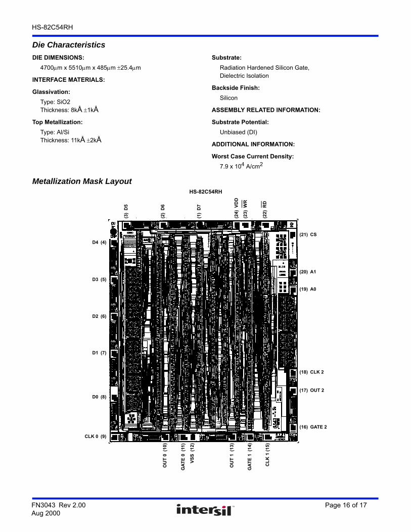
Die Characteristics
DIE DIMENSIONS:
4700m x 5510m x 485m 25.4m
INTERFACE MATERIALS:
Glassivation:
Type: SiO2Thickness: 8kÅ 1kÅ
Top Metallization:
Type: Al/SiThickness: 11kÅ 2kÅ
Substrate:
Radiation Hardened Silicon Gate,Dielectric Isolation
Backside Finish:
Silicon
ASSEMBLY RELATED INFORMATION:
Substrate Potential:
Unbiased (DI)
ADDITIONAL INFORMATION:
Worst Case Current Density:
7.9 x 10⁴ A/cm2
Metallization Mask LayoutHS-82C54RH
(3)
D5
(2)
D6
(1)
D7
(24
)V
DD
(23
)W
R
(22
)R
D
(21) CS
(20) A1
(19) A0
(18) CLK 2
(17) OUT 2
(16) GATE 2
OU
T 0
(10
)
GA
TE
0(1
1)
VS
S(1
2)
OU
T 1
(13
)
GA
TE
1(1
4)
D4 (4)
D3 (5)
D2 (6)
D1 (7)
D0 (8)
CLK 0 (9)
CL
K 1
(1
5)
FN3043 Rev 2.00 Page 16 of 17Aug 2000

FN3043 Rev 2.00 Page 17 of 17Aug 2000
HS-82C54RH
Intersil products are manufactured, assembled and tested utilizing ISO9001 quality systems as notedin the quality certifications found at www.intersil.com/en/support/qualandreliability.html
Intersil products are sold by description only. Intersil may modify the circuit design and/or specifications of products at any time without notice, provided that such modification does not, in Intersil's sole judgment, affect the form, fit or function of the product. Accordingly, the reader is cautioned to verify that datasheets are current before placing orders. Information furnished by Intersil is believed to be accurate and reliable. However, no responsibility is assumed by Intersil or its subsidiaries for its use; nor for any infringements of patents or other rights of third parties which may result from its use. No license is granted by implication or otherwise under any patent or patent rights of Intersil or its subsidiaries.
For information regarding Intersil Corporation and its products, see www.intersil.com
For additional products, see www.intersil.com/en/products.html
© Copyright Intersil Americas LLC 2000. All Rights Reserved.All trademarks and registered trademarks are the property of their respective owners.