Embed Size (px)
Citation preview

Magnetic Field Probes: What it is and
how to make it (if you don’t want to
buy it) Marquette University Microwave Seminar
May 2nd 2014
Presentation by: Khairul Aidi Zainal
Content
A. Introduction
B. Types of radiation : Differential mode and Common mode
C. Refresher on Near field VS Far field
D. How do near field Magnetic field probe work?
E. Where can I get one?
F. Show and tell
G. Conclusion
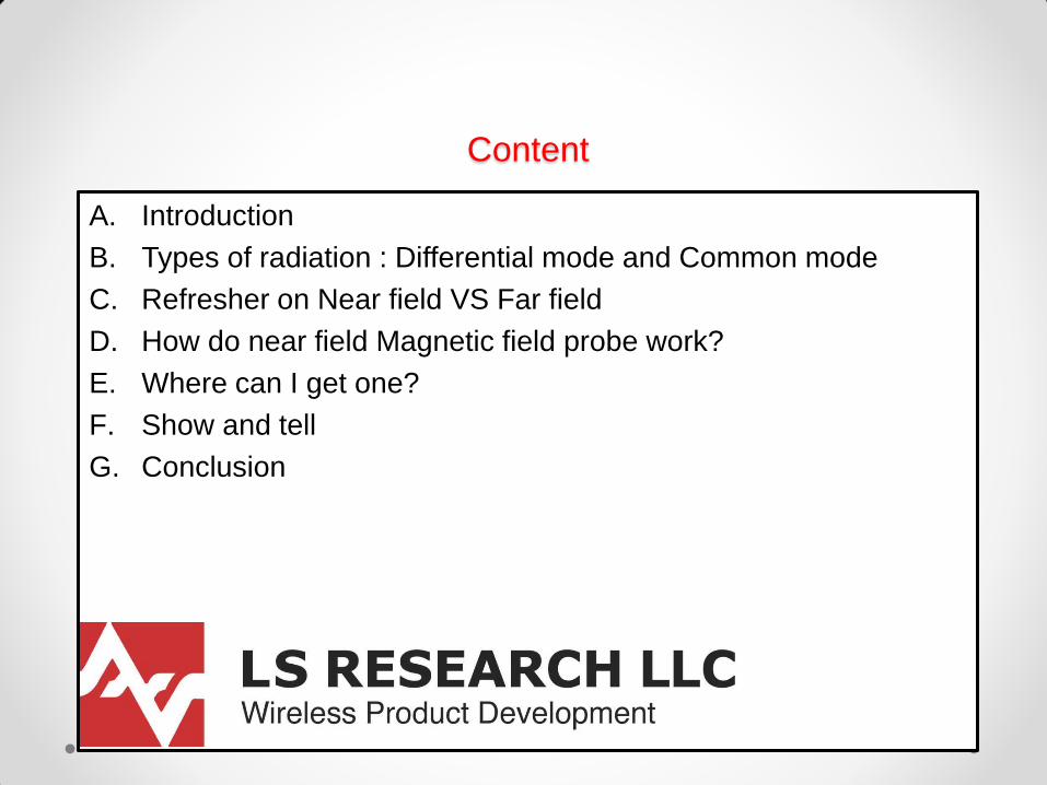
Introduction • EMC: Electromagnetic compatibility
o The art of making sure your stuff does not mess with other stuff and making
sure that other stuff cannot mess with your stuff.
o Consumer devices in the US; FCC doesn’t really care about the latter
o Federal governments set up standards: FCC has CFR title 47 part 15,
Canada has RSS (Radio Standards Specification), ICES (Interference
causing equipment standard) the rest of the world has their own ETSI,
CISPR, AS/NZS, etc.
• Your stuff should not mess with other people’s stuff o Radiated emissions need to be below limits that have been set out by the
regulatory bodies
o Conducted emissions also need to be compliant to limit
• Conducted emissions o When you plug something into the wall socket, you don’t cause your
blender to make you a smoothie.

• Radiated emissions: o Far field measurement of emissions from a product between the
frequency range 30 MHz to 40GHz.
• 3m, 10m even 30 meter measurements
• OATS or SAC
o #1 cause of product failures
• Economics of the design
• Many university do not teach proper EMC design
• Incorporate other components that do not have proper EMC design
• Bad luck
• Troubleshooting failures o Perform near field test:
• Pin point exact location of a component, trace or area of high emissions
• Predict radiated EMC results (requires software, characterization of tools/equipment, etc)
• Check to ensure fixes have effect
o Two types of near field probes (Electric and Magnetic field)
• Type of probe used is based on type of radiation
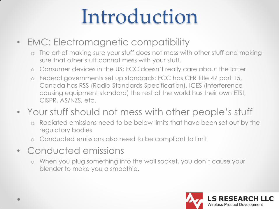
Type of Radiation • Two types of radiation
o Differential mode
o Common mode
• Differential mode radiation o Result of the normal operation of the circuit: signals travelling through
circuit loops. The larger the loop, the stronger the fundamental and harmonic emissions will be.
o Radiation can be modeled as small loop antennas
o Use magnetic field probe to detect
• Common mode radiation o Result of parasitics in the circuit; voltage drops in the conductor.
o Harder to understand and control since it was not intentionally designed into the system
o Most common form of radiation is from cables
o Radiation can be modeled as a dipole or monopole driven by noise voltage
o Current probes or electric field probe to detect
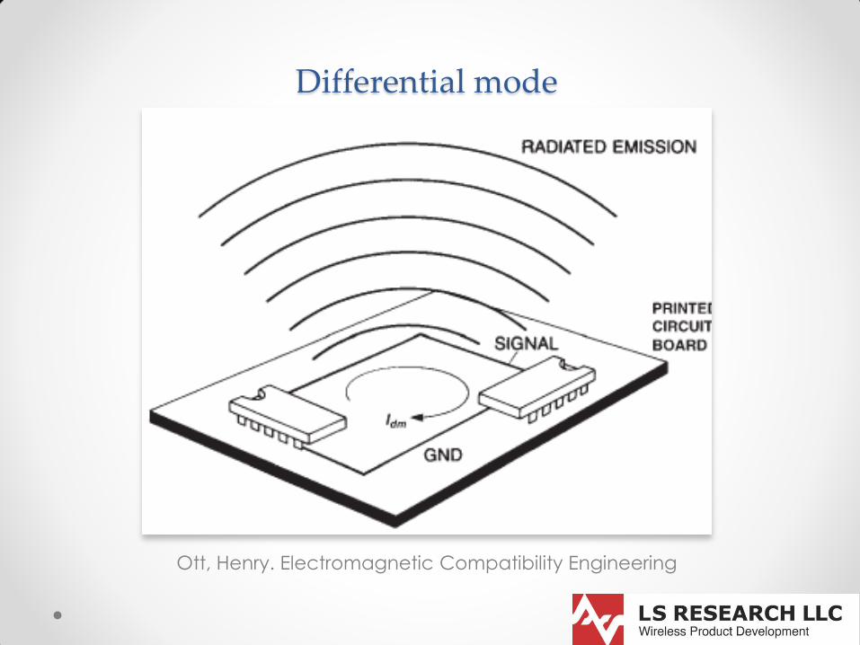
Differential mode
Ott, Henry. Electromagnetic Compatibility Engineering
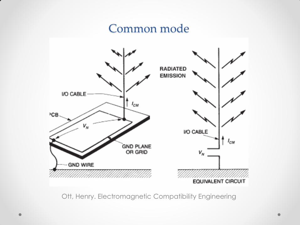
Common mode
Ott, Henry. Electromagnetic Compatibility Engineering
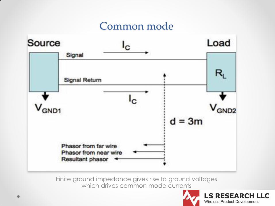
Common mode
Finite ground impedance gives rise to ground voltages which drives common mode currents
Near Field VS Far field • Compliance measurements performed in the far
field (Fraunhofer region) o In this region, the nature of the EM fields are predictable (dependent on
source, the distance from the source and the properties of the material
between the source [air])
• As we get closer to the source of emissions, near
field (Fresnel region), the field produced is mainly a
function of the properties of the source. o Object with high current, low voltage: Magnetic field
o Object with high voltage, low current: Electric field
o Note that there is no such thing as purely electric or purely magnetic field.
o Since the ratio of E and H are not constant (like in far field) we consider
the E and H field separately

• Magnetic source:
• Electric Source:
• H-field: wave impedance starts low and increases
• E-field: wave impedance starts high and decreases
• This change in wave impedance happens because
as the distance from the source increases each
field begins to produce its complimentary field
• d>>λ + d>>D + d>2D2/λ to be in the far field.
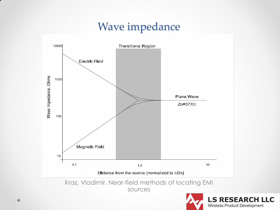
Wave impedance
Kraz, Vladimir. Near-field methods of locating EMI sources

How to H field probes work?
• Essentially an electrically small loop antenna o What applies to electrically small loop antennas apply to H field probe
o Since electrically small, current is constant around the loop with zero
phase around the loop: Shape of loop does not matter, only depends on
current and area.
• A magnetic field passing through the probe loop
generates a voltage (Farady’s law) o Induced voltage is proportional to the rate of change of magnetic flux
through a circuit loop.
• 𝑽 = 𝟐𝝅𝒇𝑩A
• Diameter of the loop determines: o Sensitivity of the probe
o Frequency response
o Spatial resolution
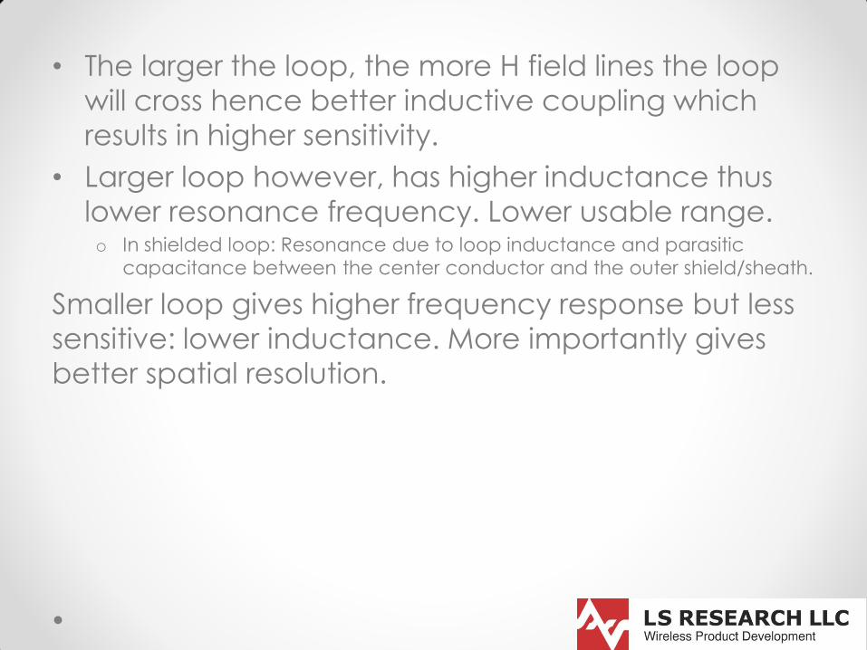
• The larger the loop, the more H field lines the loop
will cross hence better inductive coupling which
results in higher sensitivity.
• Larger loop however, has higher inductance thus
lower resonance frequency. Lower usable range. o In shielded loop: Resonance due to loop inductance and parasitic
capacitance between the center conductor and the outer shield/sheath.
Smaller loop gives higher frequency response but less
sensitive: lower inductance. More importantly gives
better spatial resolution.

Douglas C. Smith. Signal and noise measurement
techniques.
• (inductive volatge drop across the current carrying
conductor)e1=𝐿𝑑𝑖(𝑡)
𝑑𝑡
o L=inductance/unit length • (open ckt induced voltage)
e2=M𝑑𝑖(𝑡)
𝑑𝑡
o M=mutual inductance between the conductor and loop
• M is always lower than L, hence the induced voltage is the lower bound estimate.
• Square loop held
adjacent to a current
carrying conductor
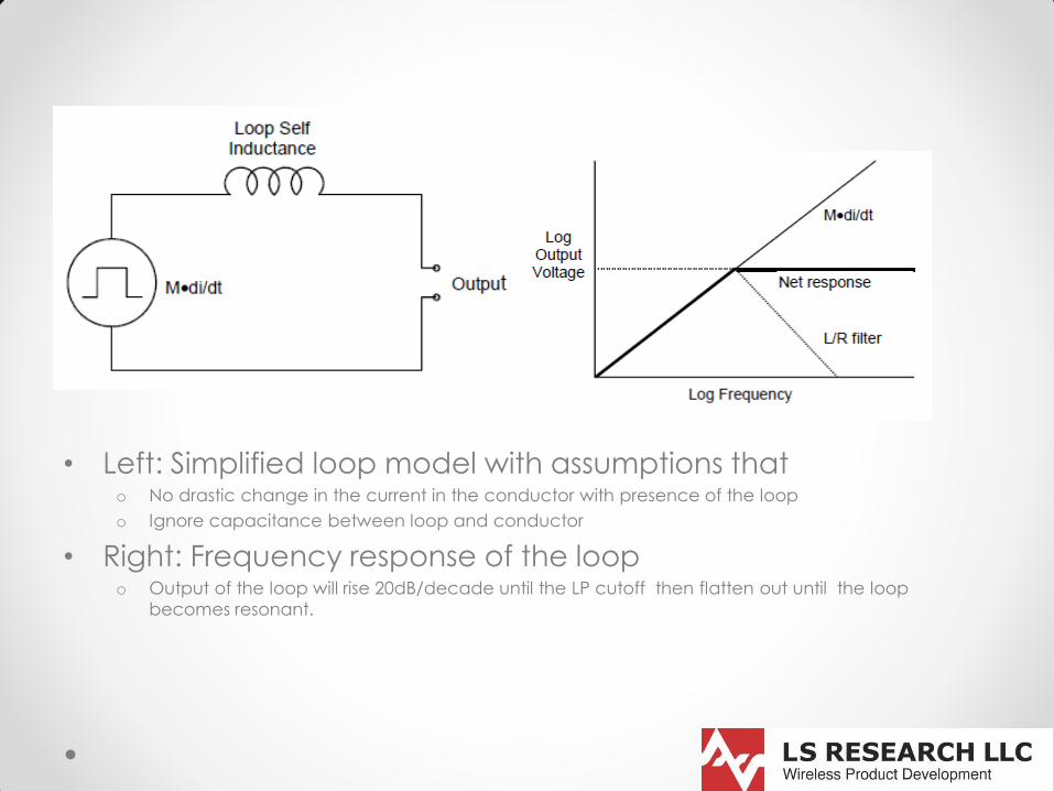
• Left: Simplified loop model with assumptions that o No drastic change in the current in the conductor with presence of the loop
o Ignore capacitance between loop and conductor
• Right: Frequency response of the loop o Output of the loop will rise 20dB/decade until the LP cutoff then flatten out until the loop
becomes resonant.
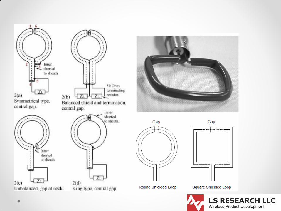
Shielded VS Unshielded
• Depends
• Shielded: o Used fro many EMC applications
o for electric field shielding
o prevent shield currents from flowing around the loop
o These currents may cancel incident magnetic field to a large
extent. Voltage will not be developed in the center conductor.
• Un-Shielded: o Circuit level measurements, this works well
o Loop can be positioned closer to the circuit being measured resulting in
higher sensitivity.
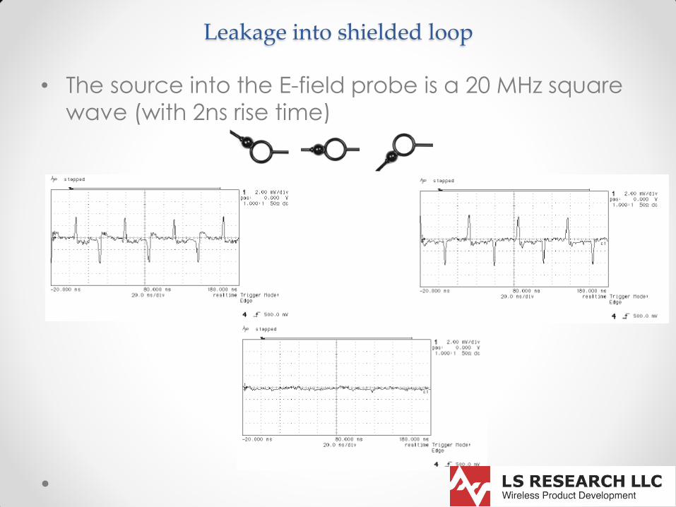
Leakage into shielded loop
• The source into the E-field probe is a 20 MHz square
wave (with 2ns rise time)
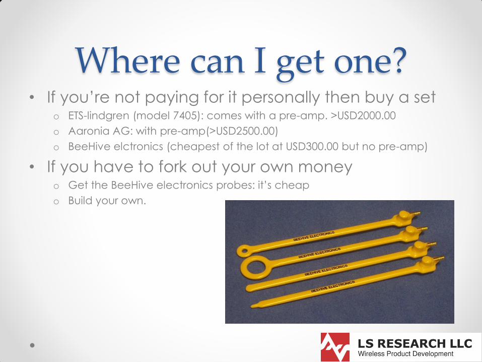
Where can I get one? • If you’re not paying for it personally then buy a set
o ETS-lindgren (model 7405): comes with a pre-amp. >USD2000.00
o Aaronia AG: with pre-amp(>USD2500.00)
o BeeHive elctronics (cheapest of the lot at USD300.00 but no pre-amp)
• If you have to fork out your own money o Get the BeeHive electronics probes: it’s cheap
o Build your own.
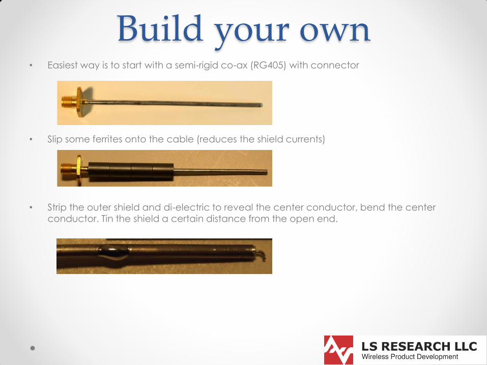
Build your own • Easiest way is to start with a semi-rigid co-ax (RG405) with connector
• Slip some ferrites onto the cable (reduces the shield currents)
• Strip the outer shield and di-electric to reveal the center conductor, bend the center conductor. Tin the shield a certain distance from the open end.
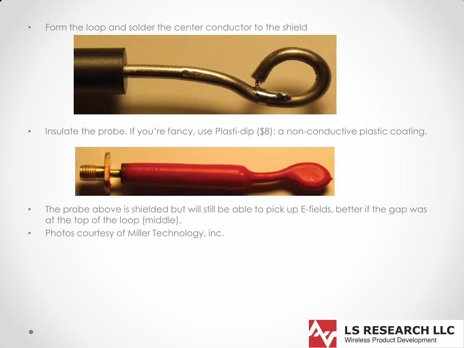
• Form the loop and solder the center conductor to the shield
• Insulate the probe. If you’re fancy, use Plasti-dip ($8): a non-conductive plastic coating.
• The probe above is shielded but will still be able to pick up E-fields, better if the gap was
at the top of the loop (middle).
• Photos courtesy of Miller Technology, inc.
Show and Tell
Conclusions • Designing for regulatory compliance (on the front
end) is a Pain in the neck but : o It’s a lot worse when design is complete and its failing…which it will
anyway.
• One of the tools that is needed in any
troubleshooting kit is a set of near field probes: o Helps pin-point location of offending component, circuit area or trace
o Find leakage on enclosures, cables and connectors
o Find sources of interference preventing a product from functioning
properly
o Predict radiated EMC test results (too complicated but do-able)
• When using other people’s money: buy it
• When using your own: build it.