Embed Size (px)
Citation preview
How to Lower Gain and Offset Drift of a Load Cellby using TKGain and TKOffset factors of PSØ8/ PSØ81
February 2010, 1st RevisionDocument-No. WP002 V1.1
White Paper
by using TKGain and TKOffset factors of PSØ8/ PSØ81
acam-messelectronic gmbh - Am Hasenbiel 27 - D-76297 Stutensee-Blankenloch - Germany - www.acam.de 1
In application note 18 we showed that the PSØ8 plays in the premier league in respect
of the gain and offset drift behavior. It was proved that a PSØ8 based electronics is good
enough to build legal for trade scales with up to 10,000 OIML1) divisions or even more.
But the gain and offset drift of the electronics is only one part of the gain and offset error
of a weigh scale. Another part comes from the load cell itself. Since the last 10 years,
the weighing electronic has benefited a lot from the significant progress in high end
converter technology. The resolution was improved and in parallel the gain and offset
errors were reduced to very low values. As a result, the load cell becomes more and
more the dominant part as cause of the gain and offset errors of a scale.
Thus, the overall temperature drift behavior of a weigh scale can not really be improved
by only reducing the error of the electronics, e.g. by reducing the offset drift from
10 nV/K to 5 nV/K. The load cell itself still has a 100 nV/K drift.
Nowadays, good converters have a far better behavior in regards of
• Gain drift
• Offset drift
• Nonlinearity
• Hysteresis
than good load cells. Only in regards of the noise behavior even the best high end con-
verters are still 1 to 2 bit below the thermal noise of the strain gage resistors and
further improvement in this respect does make sense.
PICOSTRAIN offers new possibilities to lower the gain and offset drift behavior of the load
cell by setting 2 parameters in the chip. This leads to an adjustment of the load cell that
is more precise than with standard solutions – and simplifies the production (and reduces
production cost this way) as a secondary effect. This opens new oppportunities for scale
and load cell manufacturers to improve their products while saving costs.
This white paper explains the background and shows how to do the the adjustment in
practice.
Preface
1) OIML = Organisation Internationale de Métrologie Légale, is an international organization which gives rules and guidelines for legal metrology. Please see www.oiml.org for more information.
acam-messelectronic gmbh - Am Hasenbiel 27 - D-76297 Stutensee-Blankenloch - Germany - www.acam.de 2
Preface
In August 2008, acam has done load cell adjustments in the manner we describe here.
We show and discuss the results of those in the 4th chapter of this white paper. The
measurements were done with the PSØ8 evaluation kit using the high end plug-in module
and various load cells.
In February 2010 we added latest information according to insights gained from further
practical tests. Information added is about the possiblities to connect Rspan and its general
behavior towards the overall linearity of the load cell over temperature.
Authors: Augustin Braun, Ralf Emberger
acam-messelectronic gmbh - Am Hasenbiel 27 - D-76297 Stutensee-Blankenloch - Germany - www.acam.de 3
Preface 1
1. Gain and offset drift adjustment of the load cell with A/D converter 4
1.1 Setup 4
1.2 Measuring the strain 4
1.3 Gain drift compensation 4
1.3.1 Rspan adjustment resistors 6
1.4 Offset drift compensation 7
1.4.1 Offset drift caused by unadjusted output voltage 8
1.4.2 Offset drift caused by the drift of the strain gages 9
1.5 Conclusion 9
2. Gain and offset drift adjustment of the load cell with PICOSTRAIN 10
2.1 Setup 10
2.2 PICOSTRAIN measurement principle 12
2.3 Gain drift compensation (TKGain) 13
2.3.1 Nonlinearity of gain over temperature 15
2.4 Offset drift compensation (TKOffset) 16
2.4.1 Without temperature drift run (partly compensated) 17
2.4.2 With temperature drift run (full compensated) 18
3. How to perform the gain and offset adjustment with PICOSTRAIN 20
3.1 Without temperature drift run (partly compensated) 20
3.2 With temperature drift run 20
3.2.1 Doing only offset drift compensation (TKOffset) 21
3.2.2 Doing gain and offset drift compensation (TKGain and TKOffset) 24
3.2.3 Discussion of results 27
3.3 Conclusion 28
4. Load cell adjustments in practice 29
4.1 Applied on an HBM-SP4C3 load cell 29
4.2 Applied on CZL-601 load cells 32
4.3 Conclusion 35
Index
acam-messelectronic gmbh - Am Hasenbiel 27 - D-76297 Stutensee-Blankenloch - Germany - www.acam.de 4
At first, we look at the well-known classical A/D converter solutions.
1.1 Setup
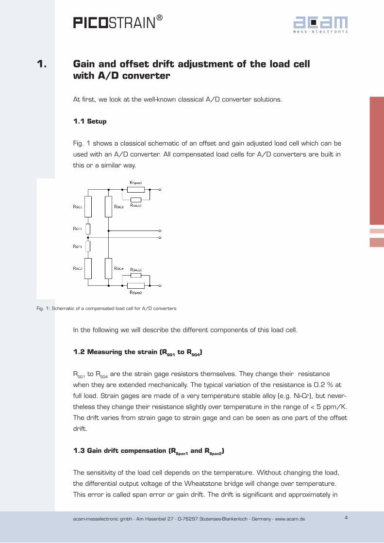
Fig. 1 shows a classical schematic of an offset and gain adjusted load cell which can be
used with an A/D converter. All compensated load cells for A/D converters are built in
this or a similar way.
1. Gain and offset drift adjustment of the load cell with A/D converter
In the following we will describe the different components of this load cell.
1.2 Measuring the strain (RSG1 to RSG4)
RSG1 to RSG4 are the strain gage resistors themselves. They change their resistance
when they are extended mechanically. The typical variation of the resistance is 0.2 % at
full load. Strain gages are made of a very temperature stable alloy (e.g. Ni-Cr), but never-
theless they change their resistance slightly over temperature in the range of < 5 ppm/K.
The drift varies from strain gage to strain gage and can be seen as one part of the offset
drift.
1.3 Gain drift compensation (RSpan1 and RSpan2)
The sensitivity of the load cell depends on the temperature. Without changing the load,
the differential output voltage of the Wheatstone bridge will change over temperature.
This error is called span error or gain drift. The drift is significant and approximately in
Fig. 1: Schematic of a compensated load cell for A/D converters
acam-messelectronic gmbh - Am Hasenbiel 27 - D-76297 Stutensee-Blankenloch - Germany - www.acam.de 5
1. Gain and offset drift adjustment of the load cell with A/D converter
the range of typically 300 to 600 ppm/K. Without compensation, no precise measure-
ment can be done, especially in weigh scales where the resolution is nowadays in the
range of 10 to 20 ppm of full scale (F.S.).
Example:
If an uncompensated load cell of 10,000 g capacity has a gain drift of 500 ppm/K, it
will drift 150 g (!) over a temperature range of 30 K. Thereby, the characteristic of the
drift is mostly positive, that means with increasing temperature also the sensitivity in-
creases. For a 3,000 divisions weigh scales only 0.05 % gain drift is allowed according
to OIML. This is approximately 30 times less than an uncompensated load cell has.
To compensate for this span error, either one or two temperature dependent resistors
(RSpan1, RSpan2) are added to the load cell. The basic working principle is, that the span re-
sistor’s value increases with rising temperature. So the effective voltage over the bridge
(UBr) is reduced. Consequently, also the differential output voltage (Udiff) is reduced. This
way, the increasing sensitivity of the strain gage resistors can be compensated by reduc-
ing the voltage by means of the RSpan resistors. Of course, the values of the Rspan resis-
tors have to be matched to the bridge’s drift behavior. The load cell voltage (ULC) itself is
stable over temperature.
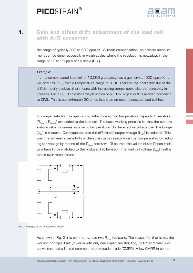
Fig. 2: Voltages of the Wheatstone bridge
As shown in Fig. 2 it is common to use two Rspan resistors. The reason for that is not the
working principle itself (it works with only one Rspan resistor, too), but that former A/D
converters had a limited common mode rejection ratio (CMRR). A low CMRR in combi-
acam-messelectronic gmbh - Am Hasenbiel 27 - D-76297 Stutensee-Blankenloch - Germany - www.acam.de 6
nation with only one Rspan resistor leads to an unwanted variation in the absolute value
of the output voltage. While only a differential voltage variation around the half supply
voltage is desired, this leads to an offset drift of the A/D converter. The effect is stronger
with a lower CMRR.
Example:
Coming back to the uncompensated load cell with a gain drift of 500 ppm/K, this
means a change in sensitivity of 1.5 % over a 30 K temperature range. In other words,
this is the increase of the sensitivity which needs to be compensated by the Rspan
resistor. With only one Rspan resistor, this results in a common mode voltage of
37.5 mV at 5 V excitation voltage. With an A/D converter with a CMRR of 80dB this
37.5 mV result in a variation of the output voltage of 3.75 µV or 125 nV/K. This can
not be neglected. For an A/D converter with a CMRR of 100dB, the variation is only
375 nV or 12.5 nV/K, which is in an acceptable value.
Because of the fact, that good A/D converter nowadays have a CMRR of at least 100 dB
there is practically no need to use the two Rspan resistors anymore. But because it was
necessary in former times with older electronics it is still common practice today.
1.3.1 Rspan adjustment resistors (RSAdj1 and RSAdj2)
The Rspan resistor itself is a special, temperature-dependent resistor which is located
very near by the strain gage resistors. It is very difficult to access and adjust these
Rspan resistors during production, therfore their value is simply corrected by paralleling
standard resistors in the connection field of the load cell. In other words, the value of
Rspan is always chosen too high (overcompensation), so that it can be reduced by a par-
alleling a resistor afterwards.
A second effect of the adjustment resistors is to counteract against the load cell’s
nonlinearity over temperature. Thereby the paralleling of the resistors introduce a nonlin-
earity over temperature (simply due to mathematics) which normally goes in the opposite
1. Gain and offset drift adjustment of the load cell with A/D converter

acam-messelectronic gmbh - Am Hasenbiel 27 - D-76297 Stutensee-Blankenloch - Germany - www.acam.de 7
direction of the load cell’s nonlinearity so that overall nonlinearity can be reduced. The
following graph illustrates the effect:
Remark: If the load cell has a very low nonlinearity over temperature it may not be
necessary to balance it by paralleling an Rspan adjustment resistor. However it is com-
mon to have an Rspan adjustment in many cases to trim the value of Rspan anyway.
Furthermore please recognize that the described nonlinearity caused by the parallel resis-
tor of Rspan is an effect over temperature and not over the load. The normally specified
nonlinearity (over the load) is not affected by this resistor.
1.4 Offset drift compensation (ROff1 and ROff2)
To adjust the offset drift it is necessary to add some resistors. Fig. 1 shows one way how
this can be done with ROff1 and ROff2.
The total offset drift is a combination of two effects which are independent from each
other:
• Offset drift due to the unadjusted zero output voltage of the bridge
• Offset drift due to the different temperature drifts of the four strain gage resistors
1. Gain and offset drift adjustment of the load cell with A/D converter
acam-messelectronic gmbh - Am Hasenbiel 27 - D-76297 Stutensee-Blankenloch - Germany - www.acam.de 8
1. Gain and offset drift adjustment of the load cell with A/D converter
1.4.1 Offset drift caused by unadjusted output voltage
In a classical A/D converter circuit it is obligatory to adjust the output voltage of the
bridge (Udiff) very close to zero (unloaded case), especially if an Rspan resistor is used.
Otherwise, there will be an additional offset drift according to the unadjusted zero
voltage.
But what happens, if the zero voltage is not adjusted ?
If there is an unadjusted offset voltage at zero load, it will be affected by the Rspan resistors.
As the Rspan resistor(s) increases over temperature, this offset voltage will decrease in
consequence. This change will be seen as offset drift in the output voltage. Depending on
the size of the unadjusted zero voltage the resulting drift can be significant, as the follow-
ing example shows:
Example:
Excitation Voltage: 5 V
Unadjusted zero offset voltage: 0.4 mV/V
Ubr variation due to Rspan: 1.5 % over 30 K
➝ Resulting offset drift: 2 mV * 1.5 % = 30 µV over 30 K, that means 1000 nV/K
If we consider that a good C3 load cell has an offset drift of approx. 100 nV/K, it is clear
that the offset drift due to Rspan from the example is 10 times higher and far too much,
even though the assumed unadjusted offset voltage of 0.4 mV/V is rather optimistic
than pessimistic and hard to reach in reality. So it is quite obvious that classical A/D con-
verter solutions do not achieve good zero offset drift behavior without adjusting the zero
offset of the bridge.
acam-messelectronic gmbh - Am Hasenbiel 27 - D-76297 Stutensee-Blankenloch - Germany - www.acam.de 9
1.4.2 Offset drift caused by the temperature drift of the strain gages
Strain gage resistors belong to the resistor types with the lowest temperature drift in
industry in general. Nevertheless, their drift is not zero. It is not the drift of each resistor
itself that causes an offset drift of the bridge but the mismatching drift of the four
resistors.
A short example shows the effect:
Drift mismatch of the 4 strain gage resistors: 0.5 ppm/K
➝ Resulting offset drift: 2.5 µV/K at 5V bridge voltage (UBr)
Thereby, 2.5 µV/K is 5 times higher than the limit given by the 3,000 division OIML
specification. To achieve a matching of 0.5 ppm/K with standard resistors is already
hard to reach and does definitely increase production costs. On the contrary, 0.5 ppm/K
mismatch in a load cell is very poor and is already reached by standard consumer cells.
That means, especially in the field of load cells the problem is widely known and products
are available with very small mismatching. A good load cell has approximately 100 nV/K
or 0.02 ppm/K mismatch which is an impressive value. But as the example shows, such
good values are required for a low offset drift.
It is clear that ROff1 and ROff2 are obligatory for a good offset drift value. It is common
practice not only to use them, but make one of the two resistors temperature dependent
in order to make a so called ‘active offset drift adjustment’. If this method is used, every
single load cell needs to be adjusted in a temperature drift run as the offset drift is not
stable over a whole production lot. In other words, every load cell has it’s own offset drift
behavior.
1.5 Conclusion
In chapter 1 we showed how the gain and offset drift compensation is done in classical
A/D converter solutions. It is obvious that without doing the compensation, limits given
by the OIML specification (or similar) are exceeded significantly. So it is obligatory to do
this compensation in order to get a reasonable drift behavior. This causes a lot of efforts
and production costs (trimming of resistors, temperature runs, etc.).
1. Gain and offset drift adjustment of the load cell with A/D converter

acam-messelectronic gmbh - Am Hasenbiel 27 - D-76297 Stutensee-Blankenloch - Germany - www.acam.de 10
2. Gain and offset drift adjustment of the load cell with PICOSTRAIN
Now we will see how this works with PICOSTRAIN. As mentioned in the preface,
PICOSTRAIN offers new possibilities to adjust the gain and offset drift of a load cell –
without any mechanical trimming.
2.1 Setup
The next figure shows the schematic of the fully compensated PICOSTRAIN bridge in com-
parison with the classical solution. It is obvious, that the circuit is much simpler than the
classical approach, instead of 6 compensation resistors only one2 is used. More than
that, this one Rspan resistor doesn’t need to have the exact value, so no mechanical
trimming is required. The fine adjustment of this resistor is entirely done by software.
Fig. 3: Classical Wheatstone bridge vs. PICOSTRAIN bridge
Fully compensated Wheatstone Bridge for
A/D-Converters
Fully compensated PICOSTRAIN bridge
A fully compensated PICOSTRAIN bridge has a much lower gain and offset drift than a
good compensated classical bridge. Furthermore, the compensation can be done faster
in production and lower the cost because no mechanical trimming is required anymore.
2) The Rspan1 resistor is good to compensate for temperature drift. It may be necessary to put another fixed resistor in parallel (Rp) to reduce the nonlinearity of the load cell over temperature. This resistor Rp is NOT the same as an adjustment resistor, it is not necessary to make an adjustment as Rspan1 is not adjusted by Rp. Please see 1.3.1 and 2.3.1 for more details.
acam-messelectronic gmbh - Am Hasenbiel 27 - D-76297 Stutensee-Blankenloch - Germany - www.acam.de 11
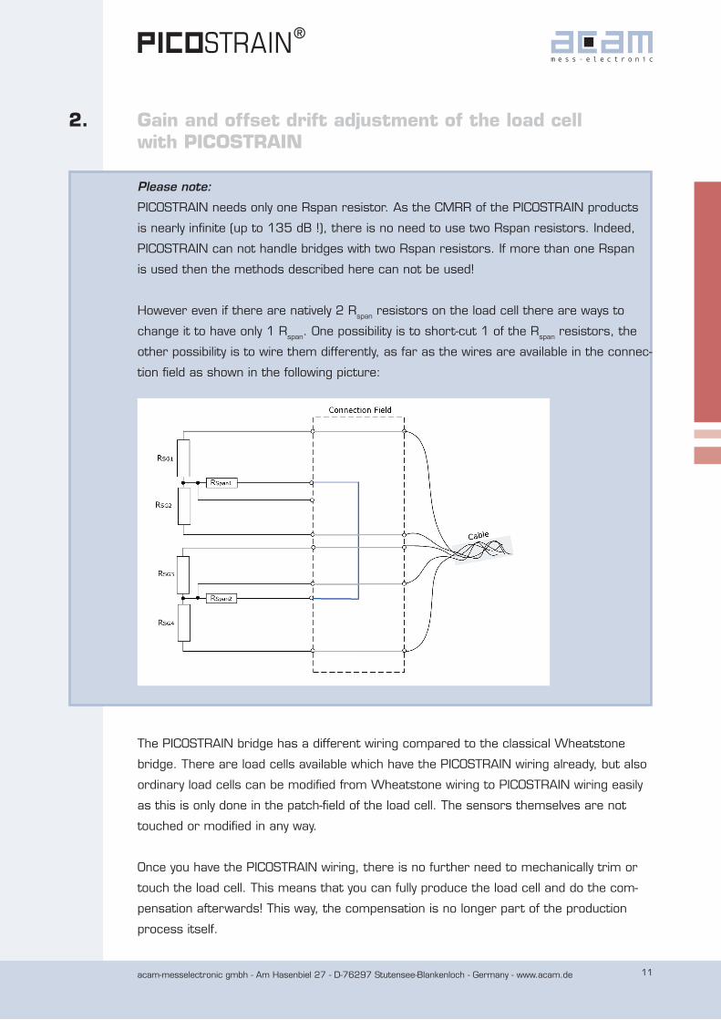
Please note:
PICOSTRAIN needs only one Rspan resistor. As the CMRR of the PICOSTRAIN products
is nearly infinite (up to 135 dB !), there is no need to use two Rspan resistors. Indeed,
PICOSTRAIN can not handle bridges with two Rspan resistors. If more than one Rspan
is used then the methods described here can not be used!
However even if there are natively 2 Rspan resistors on the load cell there are ways to
change it to have only 1 Rspan. One possibility is to short-cut 1 of the Rspan resistors, the
other possibility is to wire them differently, as far as the wires are available in the connec-
tion field as shown in the following picture:
The PICOSTRAIN bridge has a different wiring compared to the classical Wheatstone
bridge. There are load cells available which have the PICOSTRAIN wiring already, but also
ordinary load cells can be modified from Wheatstone wiring to PICOSTRAIN wiring easily
as this is only done in the patch-field of the load cell. The sensors themselves are not
touched or modified in any way.
Once you have the PICOSTRAIN wiring, there is no further need to mechanically trim or
touch the load cell. This means that you can fully produce the load cell and do the com-
pensation afterwards! This way, the compensation is no longer part of the production
process itself.
2. Gain and offset drift adjustment of the load cell with PICOSTRAIN

acam-messelectronic gmbh - Am Hasenbiel 27 - D-76297 Stutensee-Blankenloch - Germany - www.acam.de 12
Fig. 4: PICOSTRAIN bridge
2. Gain and offset drift adjustment of the load cell with PICOSTRAIN
2) acam website: http://www.acam.de/products/picostrain
You may ask how we can do a compensation fully by software? The simple answer is that
we can gain more information from the bridge as usual A/D converters. While an A/D
converter has only the information of a varying bridge output voltage, we can collect data
from every resistor thanks to the different measurement principle. In this way we can
correct mathematically the single resistor values respectively the ratios of the resistors.
Learn in the next section about the basic working principle of PICOSTRAIN and how we do
the measurement of the strain.
2.2 PICOSTRAIN measurement principle
In this section we want to give a short introduction into the PICOSTRAIN measurement
principle. A detailed explanation can be found in the data sheet of the PICOSTRAIN
products, available on the acam website2).
The capacitor Cload is charged up to supply voltage through the load pin of the chip.
Then, in a second step, Cload is discharged over one of the resistors RSG1 to RSG4 sequen-
tially by switching one of the ports P1 to P4 to ground (chip intern). The discharge time
of Cload down to a given threshold is measured with a so called time-to-digital converter
(TDC) with a resolution in the lower picosecond range (15ps). Thereby, RSG1 and RSG2 are
measured direcly while RSG3 and RSG4 are measured in combination with RSpan1.
This way RSpan1 is the only resistor needed to get the temperature information. Further-
more, this resistor is at the best place (directly on the load cell) to sense the tempera-
ture and give the information to the chip. So the efforts are minimized but the method is
very efficient.
(The methods described here are patented by acam with European and US patents)
acam-messelectronic gmbh - Am Hasenbiel 27 - D-76297 Stutensee-Blankenloch - Germany - www.acam.de 13
2.3 Gain drift compensation (TKGain)
Meanwhile a classical A/D converter solution has only one information, the differential
voltage, we can gain a lot more information with PICOSTRAIN. With some chip-internal
mathematics it is possible to get every resistor ratio of the bridge. We can even build
the ratio of Rspan to the sum of the strain gage resistors (RSG1 to RSG4).
It’s easy to imagine that we can multiply any ratio by a factor given through a register. In
particular, we are multiplying the ratio Rspan / RSG by a factor called “TKGain”, a temperature
correction factor. Doing this corresponds to a mulitplication of Rspan by TKGain. The final
output result of the bridge is then multiplied by this ‘corrected Rspan’, so that the behavior
equals a bridge with a (software) trimmed Rspan.
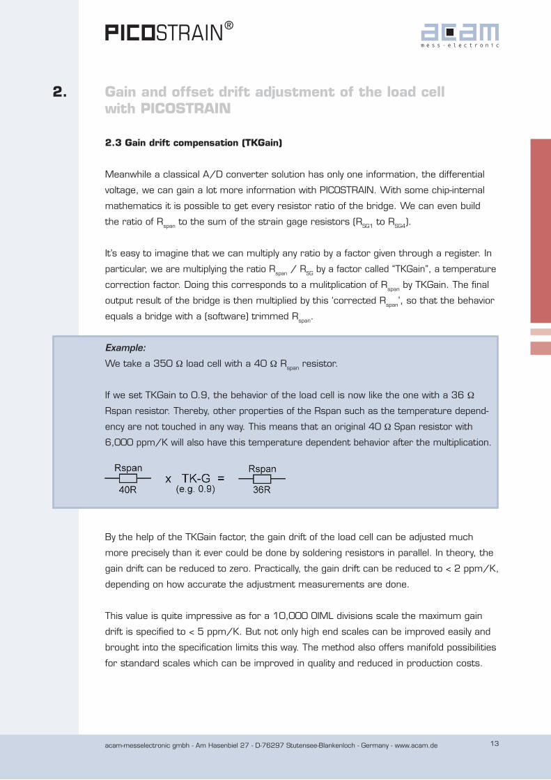
Example:
We take a 350 W load cell with a 40 W Rspan resistor.
If we set TKGain to 0.9, the behavior of the load cell is now like the one with a 36 W
Rspan resistor. Thereby, other properties of the Rspan such as the temperature depend-
ency are not touched in any way. This means that an original 40 W Span resistor with
6,000 ppm/K will also have this temperature dependent behavior after the multiplication.
By the help of the TKGain factor, the gain drift of the load cell can be adjusted much
more precisely than it ever could be done by soldering resistors in parallel. In theory, the
gain drift can be reduced to zero. Practically, the gain drift can be reduced to < 2 ppm/K,
depending on how accurate the adjustment measurements are done.
This value is quite impressive as for a 10,000 OIML divisions scale the maximum gain
drift is specified to < 5 ppm/K. But not only high end scales can be improved easily and
brought into the specification limits this way. The method also offers manifold possibilities
for standard scales which can be improved in quality and reduced in production costs.
2. Gain and offset drift adjustment of the load cell with PICOSTRAIN
acam-messelectronic gmbh - Am Hasenbiel 27 - D-76297 Stutensee-Blankenloch - Germany - www.acam.de 14
TKGain can be set in a range from –8.0 over 0.0 to 7.99999. With the TKGain value
of 1.0, the original value of the implemented Rspan is used so that the gain drift behavior
is not touched in any way. Generally, there is a wide range to set TKGain. Even negative
values can be set. This is possible due to the fact that pure mathematics is used inside
the chip. With a negative TKGain the effect of the Rspan is inversed. This may be used if an
Rspan with the ‘wrong direction’ regarding it’s temperature drift behavior is taken, but it
doesn’t make too much sense, of course.
In case you have a load cell which has already a good gain compensation (correct Rspan),
then TKGain = 1.0 is the right value to set.
Please note:
If a load cell with an Rspan resistor is used, you need to enable the ‚modification pos sibilities‘
by setting mod_rspan = 1. Even if the load cell’s original Rspan shall be used without any
further adjustment, mod_rspan needs to be set to 1 (with TKGain = 1.0
and TK-Off = 0). Setting mod_rspan = 0 is only an option for uncompensated load cells
that have no Rspan resistor at all
The absolute correct value for TKGain can be determined by doing an accurate tempera-
ture run. But even without doing the temperature run or doing it not absolutely accurately,
you can achieve the following:
• Correcting a complete lot of load cells which would have been wasted because their
gain drift is too high. This requires the determination of the proper TKGain value once
as well as a the determination if the drift behavior of the whole lot is similar.
• Correcting the Rspan resistor into the correct range. For standard scales it may not be
necessary to adapt the Rspan resistor very accurately, but it will be necessary to adapt
it to a reasonable behavior. With the software correction, the load cell production is
simplified.
2. Gain and offset drift adjustment of the load cell with PICOSTRAIN
acam-messelectronic gmbh - Am Hasenbiel 27 - D-76297 Stutensee-Blankenloch - Germany - www.acam.de 15
2. Gain and offset drift adjustment of the load cell with PICOSTRAIN
2.3.1 Nonlinearity of gain over temperature
Independently of the PICOSTRAIN gain drift compensation we have always a nonlinearity of
the load cell over temperature. This nonlinearity generally has two causes, the nonlinearity
of the load cell itself (material, glue, wiring, etc.) and a nonlinearity coming from the paral-
leling of the Rspan resistor with its adjustment resistor (Rsadj). Normally these two effects
are in opposite direction, so that overall nonlinearity can be reduced. In other words, the
nonlinearity introduced by the paralleling of the resistors is compensating to some degree
the nonlinearity coming from the load cell itself.
However there is a change in behavior if the adjustment resistor (Rsadj) is missing at all,
as there is no compensating effect of nonlinearity any longer. In the basic set-up of a
PICOSTRAIN bridge with 1 Rspan there is no further adjustment resistor needed and there-
fore missing. This is not a problem if the load cell’s nonlinearity itself is very low. But if it
has a nonlinearity not neglectable, it may be required to add a parallel resistor to com-
pensate for the nonlinearity. Please note, that this parallel resistor (Rp) does not have the
purpose of correcting Rspan in its resistor’s value, but only for nonlinear compensation of
the load cell itself.
In order to decide whether a parallel resistor is necessary or not, please check for
matching one or more of the following criteria:
• The load cell normally has an adjustment resistor and Rsadj < 10 x Rspan is true
• In the first run of determining TK-Gain you get a value < 0.8
• A temperature run with TK-Gain = 1 shows a gain drift > 100 ppm/K
Examples:
Your load cell has an Rspan of 40 W with an adjustment resistor Rsadj in parallel of 350 W.
In this case Rsadj is smaller than 10-times Rspan and so it’s recommended to keep the
resistor. You also could choose standard values like 330 W or 390 W (over complete pro-
duction).
Let’s assume you only have 1 Rspan and no adjustment resistor in parallel and you are
determining TK-Gain for the first time. If TK-Gain is smaller than 0.8, i.e. 0.73 it’s
recommended to switch a resistor in parallel (Rp).
acam-messelectronic gmbh - Am Hasenbiel 27 - D-76297 Stutensee-Blankenloch - Germany - www.acam.de 16
Please note, that the parallel resistor (Rp) can be an ordinary fixed resistor and does
NOT have to be a special kind of adjustment resistor. Of course if you have already one in
parallel which fulfills the requirements you can keep it.
The size of Rp is calculated by our TK-Gain / TK-Off calculation sheet
TKGain_TKOffs_Calculation.xls available from our website at:
http://www.acam.de/fileadmin/Download/_software/TKGain_TKOffs_Calculation.xls. It
is thereby not necessary to choose it exactly to the value proposed, but roughly. For
example if the calculation sheet suggests an Rp of 462.5 W you can simply pick the next
value from the E12 row which would be 470 W, even the following, 510 W would be
possible.
2.4 Offset drift compensation (TK-Off)
The mathematics of the chips is really powerful. When the bridge is recombined mathe-
matically in the CPU of the PICOSTRAIN chips. Even resistors can be virtually added that
do not exist in reality. Exactly this is done when it comes to the offset adjustment:
A resistor is added virtually and can be configured by the TKOff register. The properties
of this ‘virtual offset resistor’ are:
• absolutely precise
• set in ppm, relatively to the strain gage resistors
• can be positive or negative
• can be chosen in a very wide range (24 bit value with 0.01ppm steps)
This is indeed the most ideal resistor which can be built.
Just to make clear the dimension of this ideal resistor: if we take for example a 350 W
strain gage resistor then the minimum step size would be 3.5 µW. Doing such a resistor
trimming in reality will be pretty challenging!
2. Gain and offset drift adjustment of the load cell with PICOSTRAIN

acam-messelectronic gmbh - Am Hasenbiel 27 - D-76297 Stutensee-Blankenloch - Germany - www.acam.de 17
This virtually added resistor can adjust the offset drift of the load cell and can
compensate both parts of the drift. This is indeed an ideal offset adjustment!
2.4.1 Offset drift compensation without temperature run (partly compensated)
By means of this virtually added resistor the bridge’s zero offset can be adjusted exactly
to zero. Unlike in classical solutions, there is no need to add an offset adjustment resistor
mechanically on the load cell The adjustment is entirely done by software (register set-
ting). By adjusting the bridge to zero, at least one of the two possible causes of the offset
drift can be eliminated (see section 1.4 Offset drift compensation). The adjustment of the
bridge’s zero offset does not require a temperature run.
How can the adjustment be done ? - Two simple steps are required:
1. Unload the load cell entirely (here the ‘real zero load’ is needed, because even a slight
weight like the weighing plate will have effects on the gain drift). The best moment to
do that is during the load cell production.
2. Adjust the value for TKOff in such a way that the displayed measurement result (it’s
called HB0 at PSØ8/PSØ81) is showing zero. The checkbox ‘zero-offset’ in the evalu-
ation software needs to be unchecked before, of course. If necessary, choose negative
values for TKOff in order to adjust the value to zero.
2. Gain and offset drift adjustment of the load cell with PICOSTRAIN
Fig. 5: Adding an offset adjustment resistor virtually
acam-messelectronic gmbh - Am Hasenbiel 27 - D-76297 Stutensee-Blankenloch - Germany - www.acam.de 18
After doing this, the bridge is perfectly zero-offset adjusted. The Rspan resistor will not
cause any offset drift from now on. This method is simple and cost effective because no
temperature run is needed.
Unfortunately, this method is not sufficient when it comes to the second cause of the
offset drift: the mismatching drift of the four strain gage resistors (summary drift). So if
this part is the major cause of the offset drift, the simple adjustment described above is
not sufficient. In this case, an adjustment with a temperature run is required like described
in the next section.
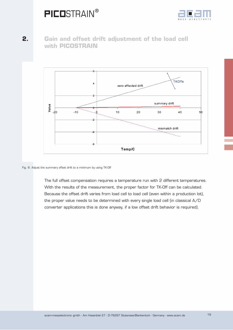
2.4.2 Offset drift compensation with temperature drift run (fully compensated)
Doing a temperature run offers the possibility to compensate both causes of the offset
drift – the unadjusted zero-offset of the bridge and also the mismatching drift of the
strain gage resistors.
You know already, that by means of the virtually added resistor the zero-offset of the
bridge can be adjusted to zero and so the influence of the Rspan in regards of the offset
drift can be minimized. But this virtual offset resistor can do more: it’s able to compen-
sate also the mismatching drift of the 4 strain gage resistors, if the TKOff value is set
correctly – in both, the value and direction (positive or negative).
In other words, the value of TKOff does combine the compensation of both drift sources.
So once the offset of the bridge is adjusted to zero, the Rspan helps indiretly to deter-
mine the offset drift caused by the mismatch of the strain gage resistors. With this pair
of information the TKOff can be set to counteract against both drift sources and reach a
low summary drift, as principally shown in Fig. 6.
2. Gain and offset drift adjustment of the load cell with PICOSTRAIN
acam-messelectronic gmbh - Am Hasenbiel 27 - D-76297 Stutensee-Blankenloch - Germany - www.acam.de 19
The full offset compensation requires a temperature run with 2 different temperatures.
With the results of the measurement, the proper factor for TK-Off can be calculated.
Because the offset drift varies from load cell to load cell (even within a production lot),
the proper value needs to be determined with every single load cell (in classical A/D
converter applications this is done anyway, if a low offset drift behavior is required).
Fig. 6: Adjust the summary offset drift to a minimum by using TK-Off
2. Gain and offset drift adjustment of the load cell with PICOSTRAIN

acam-messelectronic gmbh - Am Hasenbiel 27 - D-76297 Stutensee-Blankenloch - Germany - www.acam.de 20
3. How to do the gain and offset adjustment with PICOSTRAIN
3.1 Adjustment without temperature drift run (partly compensated)
As described, the corrections can be done without a temperature drift run but will com-
pensate the gain and offset drift only in parts.
Gain drift:
Assuming the mismatch of the Rspan is known, the resistor can be corrected by setting
the TKGain value. This can be done for a whole lot, so maybe lots out of the limits can be
saved this way.
Example: due to the measurement of some sample load cells out of a production lot in
the temperature chamber it is known that the Rspan resistors in that lot is 10 % lower
than required. But as it is a commercial scale lot, a mechanical trimming would be too
expensive and with a deviation of 10 % almost not feasible. In this case, TKGain simply
needs to be set to 1.1, so the Rspan resistor is corrected to the value needed without
any further efforts.
Offset drift:
As described in the previous section, you can eliminate the offset drift caused by the non-
adjusted zero-offset of the bridge. This can be done best during the load cell production
when no load is on the load cell at all. Then the TKOff value is modified until the bridge’s
result shows zero. This way, at least one part of the offset drift can be eleminated in a
simple manner.
Both results, the TKGain and TKOff value could be written on a small label on the load cell
itself, so that this value can be set in the registers when a PICOSTRAIN converter is
used.
3.2 Adjustment with temperature drift run (fully compensated)
A much more precise compensation can be achieved by determination of the correct
values for TKGain and TK-Off during a temperature run. Basically there is the possibility
to adjust the offset drift only or to adjust both, the gain and offset drift with one run.
acam-messelectronic gmbh - Am Hasenbiel 27 - D-76297 Stutensee-Blankenloch - Germany - www.acam.de 21
Only offset drift adjustment
In production it is usually easier to get a good adjusted gain drift than a good adjusted
offset drift. Because of this it can make sense only to adjust the offset drift more accu-
rately with TKOff.
Another case are high capacity load cells, because you hardly can run a temperature
drift test with a 1000 kg maximum load in a temperature drift chamber. Our offset drift
adjustment can be done anyway in this case.
Full adjustment
With a full adjustment the gain and offset drift is minimized all at once in one tempera-
ture run. This is the best possible compensation with PICOSTRAIN.
The temperature run requires to set two different temperatures and to let them get
settled long enough (approx. 1.5 h minimum). At each temperature some measurements
are done and the results written into an Excel-Sheet (provided by acam, available at:
http://www.acam.de/fileadmin/Download/_software/TKGain_TKOffs_Calculation.xls).
Based on these measurement results, the sheet calculates the proper TKGain and TKOff
values. The detailed steps are explained in the following two chapters:
3.2.1 Doing only offset drift compensation (TKOff)
To do the TKOff adjustment, it is important to fulfill one precondition:
Either the TKGain value is already correct (e.g. you know the Rspan is 10 % too small over
the whole charge, so it can be set to 1.1) or you set TKGain to 1.0 but do not load the
cell at all (this means, even small weights like the weighing plate needs to be removed). If
this precondition is not fulfilled, the influence of the gain drift will make it impossible to
adjust the offset drift to a minimum value.
The two temperatures should be apart far enough, with at least 30 K difference is be-
tween them, e.g. +10 °C and +40 °C.
3. How to do the gain and offset adjustment with PICOSTRAIN
acam-messelectronic gmbh - Am Hasenbiel 27 - D-76297 Stutensee-Blankenloch - Germany - www.acam.de 22
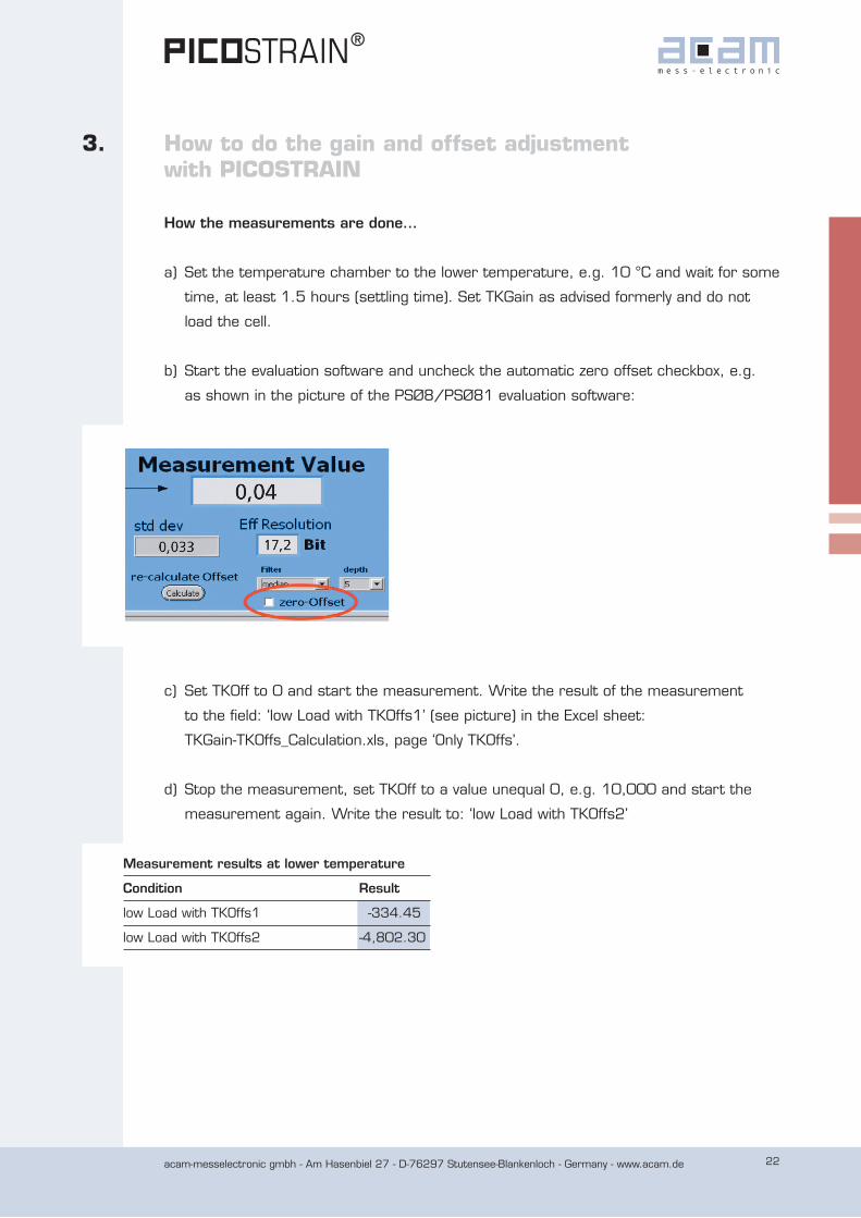
How the measurements are done…
a) Set the temperature chamber to the lower temperature, e.g. 10 °C and wait for some
time, at least 1.5 hours (settling time). Set TKGain as advised formerly and do not
load the cell.
b) Start the evaluation software and uncheck the automatic zero offset checkbox, e.g.
as shown in the picture of the PSØ8/PSØ81 evaluation software:
Measurement results at lower temperature
Condition Result
low Load with TKOffs1 -334.45
low Load with TKOffs2 -4,802.30
c) Set TKOff to 0 and start the measurement. Write the result of the measurement
to the field: ‘low Load with TKOffs1’ (see picture) in the Excel sheet:
TKGain-TKOffs_Calculation.xls, page ‘Only TKOffs’.
d) Stop the measurement, set TKOff to a value unequal 0, e.g. 10,000 and start the
measurement again. Write the result to: ‘low Load with TKOffs2’
3. How to do the gain and offset adjustment with PICOSTRAIN
acam-messelectronic gmbh - Am Hasenbiel 27 - D-76297 Stutensee-Blankenloch - Germany - www.acam.de 23
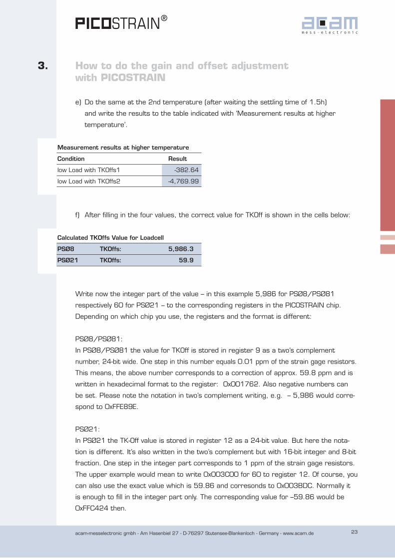
Calculated TKOffs Value for Loadcell
PSØ8 TKOffs: 5,986.3
PSØ21 TKOffs: 59.9
f) After filling in the four values, the correct value for TKOff is shown in the cells below:
3. How to do the gain and offset adjustment with PICOSTRAIN
Measurement results at higher temperature
Condition Result
low Load with TKOffs1 -382.64
low Load with TKOffs2 -4,769.99
e) Do the same at the 2nd temperature (after waiting the settling time of 1.5h)
and write the results to the table indicated with ‘Measurement results at higher
temperature’.
Write now the integer part of the value – in this example 5,986 for PSØ8/PSØ81
respectively 60 for PSØ21 – to the corresponding registers in the PICOSTRAIN chip.
Depending on which chip you use, the registers and the format is different:
PSØ8/PSØ81:
In PSØ8/PSØ81 the value for TKOff is stored in register 9 as a two’s complement
number, 24-bit wide. One step in this number equals 0.01 ppm of the strain gage resistors.
This means, the above number corresponds to a correction of approx. 59.8 ppm and is
written in hexadecimal format to the register: 0x001762. Also negative numbers can
be set. Please note the notation in two’s complement writing, e.g. – 5,986 would corre-
spond to 0xFFE89E.
PSØ21:
In PSØ21 the TK-Off value is stored in register 12 as a 24-bit value. But here the nota-
tion is different. It’s also written in the two’s complement but with 16-bit integer and 8-bit
fraction. One step in the integer part corresponds to 1 ppm of the strain gage resistors.
The upper example would mean to write 0x003C00 for 60 to register 12. Of course, you
can also use the exact value which is 59.86 and corresonds to 0x003BDC. Normally it
is enough to fill in the integer part only. The corresponding value for –59.86 would be
0xFFC424 then.
acam-messelectronic gmbh - Am Hasenbiel 27 - D-76297 Stutensee-Blankenloch - Germany - www.acam.de 24
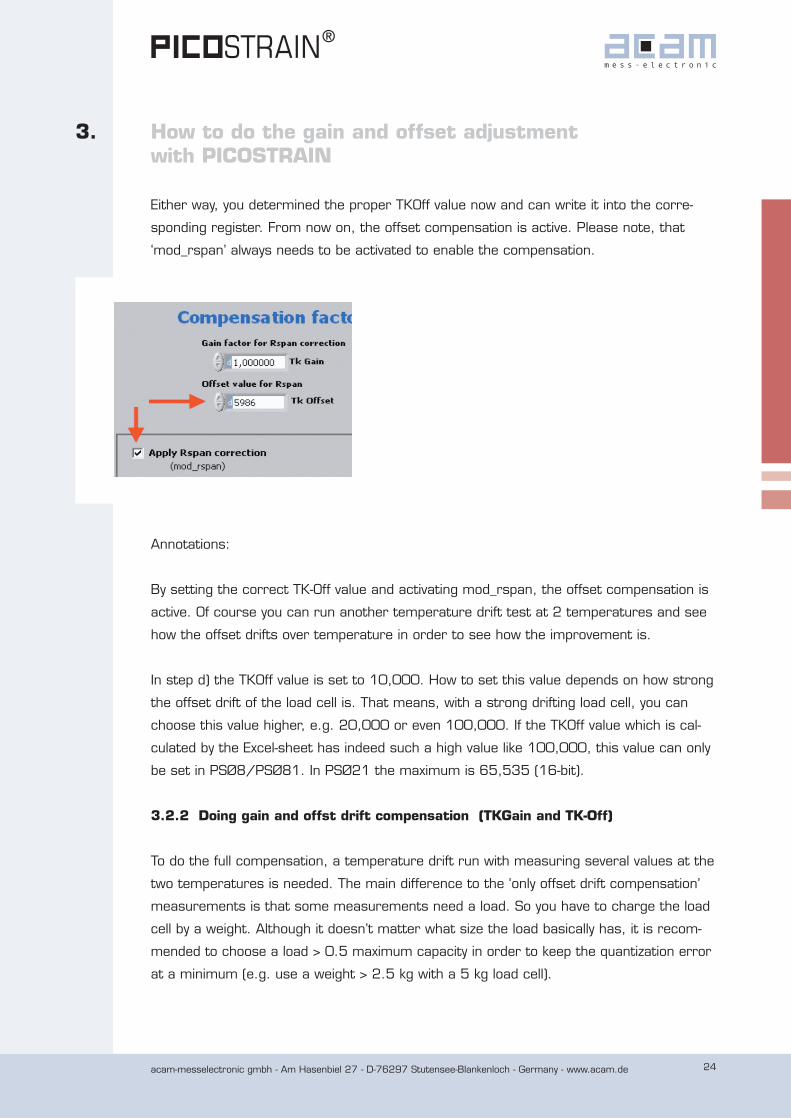
Either way, you determined the proper TKOff value now and can write it into the corre-
sponding register. From now on, the offset compensation is active. Please note, that
‘mod_rspan’ always needs to be activated to enable the compensation.
Annotations:
By setting the correct TK-Off value and activating mod_rspan, the offset compensation is
active. Of course you can run another temperature drift test at 2 temperatures and see
how the offset drifts over temperature in order to see how the improvement is.
In step d) the TKOff value is set to 10,000. How to set this value depends on how strong
the offset drift of the load cell is. That means, with a strong drifting load cell, you can
choose this value higher, e.g. 20,000 or even 100,000. If the TKOff value which is cal-
culated by the Excel-sheet has indeed such a high value like 100,000, this value can only
be set in PSØ8/PSØ81. In PSØ21 the maximum is 65,535 (16-bit).
3.2.2 Doing gain and offst drift compensation (TKGain and TK-Off)
To do the full compensation, a temperature drift run with measuring several values at the
two temperatures is needed. The main difference to the ‘only offset drift compensation’
measurements is that some measurements need a load. So you have to charge the load
cell by a weight. Although it doesn’t matter what size the load basically has, it is recom-
mended to choose a load > 0.5 maximum capacity in order to keep the quantization error
at a minimum (e.g. use a weight > 2.5 kg with a 5 kg load cell).
3. How to do the gain and offset adjustment with PICOSTRAIN

acam-messelectronic gmbh - Am Hasenbiel 27 - D-76297 Stutensee-Blankenloch - Germany - www.acam.de 25
Again, the two temperatures should be enough apart so that at least 30 K difference
is between them (e.g. +10 °C and +40 °C). Before doing the measurements at each
temperature, let the temperature get settled at least 1.5 hours. At each temperature,
5 measurements are done and the results written to the Excel sheet ‘TKGain-TKOffs_
Calculation.xls’, page ‘TKOffs and TKGain’, available at
http://www.acam.de/fileadmin/Download/_software/TKGain_TKOffs_Calculation.xls
Preliminary considerations
Before you start with the measurements, you need to pre-select a value for TKGain and
TKOff. They should be chosen in a reasonable range in order to avoid quantization errors.
But what does this mean, ‘reasonable range’ ? – Let’s give you an example:
If you have a load cell where the Rspan is already matched, then a TKGain value of 1.0
would be the right choice. If you know that it is approx. 10% too small, then you can set
TKGain to 1.1. The TKOff is chosen according to the expected offset drift. This is normally
within the range of ±1mV/V (= 1,000ppm), so the right pre-setting in PSØ8/PSØ81
would be TKOff = 100,000 or 1,000 in PSØ21.
Let’s turn attention to the charging of the load cells: some measurements require the
load cell to be charged, at least with the half weight of full scale, e.g. >2.5 kg at a 5 kg
load cell. So when we are talking about load = ‘low’ in the Excel sheet we mean the un-
loaded scale, only with the weighing plate but nothing more on it. In the fields marked
with load = ‘high’ you apply the load to the scale.
So in our example, we use PSØ8/PSØ81 and set the values in the Excel sheet accordingly:
Choosen TKGain 1.0000
Choosen TKOffs 100,000
3. How to do the gain and offset adjustment with PICOSTRAIN
acam-messelectronic gmbh - Am Hasenbiel 27 - D-76297 Stutensee-Blankenloch - Germany - www.acam.de 26
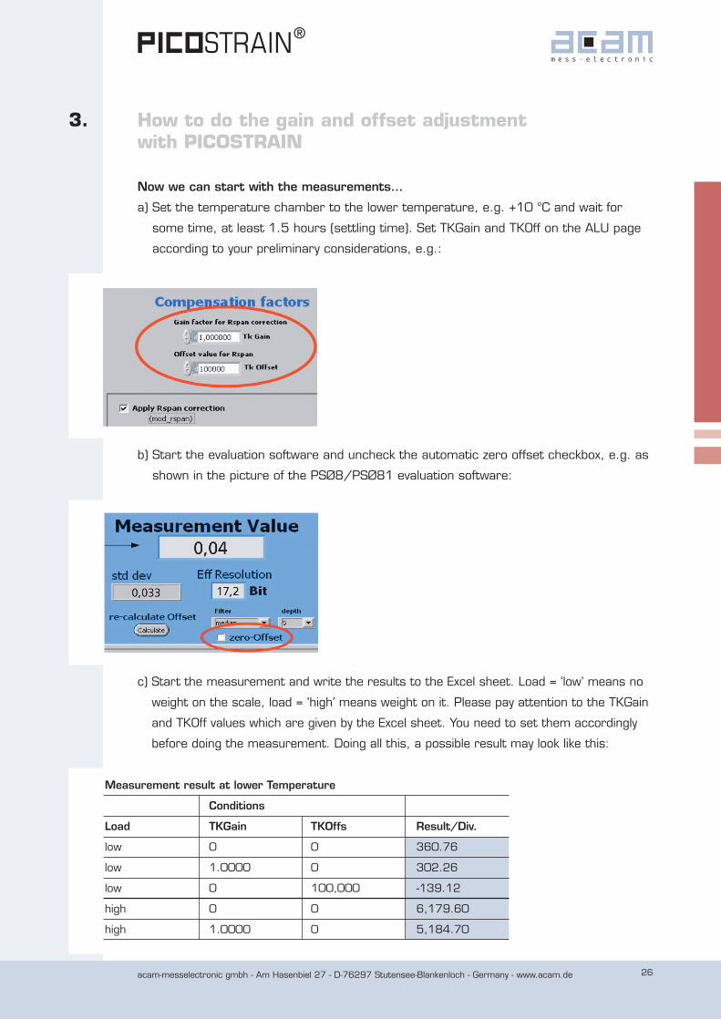
Now we can start with the measurements…
a) Set the temperature chamber to the lower temperature, e.g. +10 °C and wait for
some time, at least 1.5 hours (settling time). Set TKGain and TKOff on the ALU page
according to your preliminary considerations, e.g.:
b) Start the evaluation software and uncheck the automatic zero offset checkbox, e.g. as
shown in the picture of the PSØ8/PSØ81 evaluation software:
c) Start the measurement and write the results to the Excel sheet. Load = ‘low’ means no
weight on the scale, load = ‘high’ means weight on it. Please pay attention to the TKGain
and TKOff values which are given by the Excel sheet. You need to set them accordingly
before doing the measurement. Doing all this, a possible result may look like this:
Measurement result at lower Temperature
Conditions
Load TKGain TKOffs Result/Div.
low 0 0 360.76
low 1.0000 0 302.26
low 0 100,000 -139.12
high 0 0 6,179.60
high 1.0000 0 5,184.70
3. How to do the gain and offset adjustment with PICOSTRAIN
acam-messelectronic gmbh - Am Hasenbiel 27 - D-76297 Stutensee-Blankenloch - Germany - www.acam.de 27
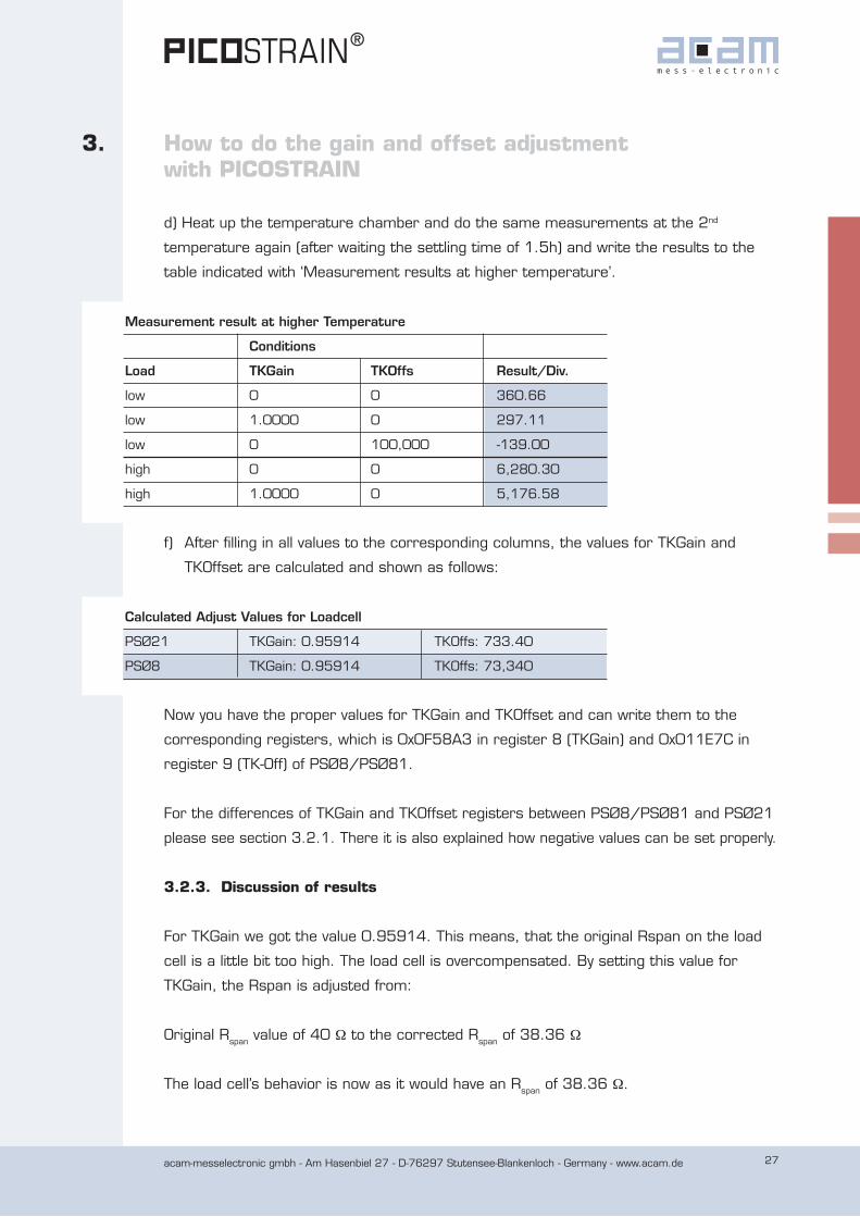
d) Heat up the temperature chamber and do the same measurements at the 2nd
temperature again (after waiting the settling time of 1.5h) and write the results to the
table indicated with ‘Measurement results at higher temperature’.
f) After filling in all values to the corresponding columns, the values for TKGain and
TKOffset are calculated and shown as follows:
3. How to do the gain and offset adjustment with PICOSTRAIN
Measurement result at higher Temperature
Conditions
Load TKGain TKOffs Result/Div.
low 0 0 360.66
low 1.0000 0 297.11
low 0 100,000 -139.00
high 0 0 6,280.30
high 1.0000 0 5,176.58
Now you have the proper values for TKGain and TKOffset and can write them to the
corresponding registers, which is 0x0F58A3 in register 8 (TKGain) and 0x011E7C in
register 9 (TK-Off) of PSØ8/PSØ81.
For the differences of TKGain and TKOffset registers between PSØ8/PSØ81 and PSØ21
please see section 3.2.1. There it is also explained how negative values can be set properly.
3.2.3. Discussion of results
For TKGain we got the value 0.95914. This means, that the original Rspan on the load
cell is a little bit too high. The load cell is overcompensated. By setting this value for
TKGain, the Rspan is adjusted from:
Original Rspan value of 40 W to the corrected Rspan of 38.36 W
The load cell’s behavior is now as it would have an Rspan of 38.36 W.
Calculated Adjust Values for Loadcell
PSØ21 TKGain: 0.95914 TKOffs: 733.40
PSØ8 TKGain: 0.95914 TKOffs: 73,340
acam-messelectronic gmbh - Am Hasenbiel 27 - D-76297 Stutensee-Blankenloch - Germany - www.acam.de 28
As the value for TKOff is unequal zero, a resistor is added virtually. The value of the
resistor corresponds to an offset shift of 733.4 ppm or in other words 0.7334 mV/V.
With this TKOff value the scale is offset adjusted from now on.
3.3 Conclusion
PICOSTRAIN offers a new and comfortable method to adjust the gain and offset drift
of a load cell only by software. This offers manifold possibilities compared with existing
A/D converter solutions because a mechanical trim is no longer needed.
We showed in chapter 3 that both, gain and offset drift, can be adjusted accurately.
The adjustment of the gain drift can always be done over the whole lot by measuring only
some sample load cells and then applying the TKGain value to all the load cells of the
same charge. To adjust the load cell’s offset drift, it is required to find the proper correc-
tion factor for each load cell which is common practice nowadys anyway (as it is normally
applied at high quality load cells or to those with a very high offset drift). The advantage
of the PICOSTRAIN method is the easy way of how the adjustment is done and that the
load cells can be partly or fully adjusted – without touching them mechanically.
We see the following advantages for the load cell manufacturers / quality of the load cell:
• Achieve a good gain and offset drift behavior
• Adjust the load cells more accurate than it can’t be done today
• No mechanical trim is needed anymore
• Because of the simplified method you save time and costs in production
• The load cell itself gets simplified (lower complexity due to less resistors)
These advantages offer new possibilities in the production:
• As the adjustment is easier it can be done at any place (e.g. different branches)
• It generally increases the quality in production
• Costs are lowered due to less efforts and lower number of compensation resistors
• Aged or misadjusted load cells can be ‘re-adjusted’
We at acam believe that this new method of temperature compensation just by software
brings many benefits to the manufacturers. In short words, the quality is increased by less
efforts and money. The method is really valuable for load cell and scale manufacturers.
3. How to do the gain and offset adjustment with PICOSTRAIN

acam-messelectronic gmbh - Am Hasenbiel 27 - D-76297 Stutensee-Blankenloch - Germany - www.acam.de 29
4. Load cell adjustment in practice
In this last chapter we want to describe the results which we gained from doing the tem-
perature compensation following the discussed method. Therefore, we adjusted 4 load
cells here at acam in August 2008. The results are given here and are discussed shortly
in the conclusion.
All measurements have been done with the PSØ8 evalution kit and the high resolution
plug-in module. We applied the compensation on 1 HBM load cell and on 3 CZL load
cells, which are simply standard C3 load cells with PICOSTRAIN wiring as we deliver them
with the evaluation kit.
4.1 Applied on an HBM-SP4C3 load cell
Setup
An ordinary HBM load cell (type: SP4C3) was taken and modified to PICOSTRAIN wiring.
To get the PICOSTRAIN wiring the connections were changed in the connection field of
the load cell. Except one Rspan resistor and its corresponding adjustment resistor Rsadj1
all the other compensation resistors were removed. The original load cell had 2 Rspan
resistors each paralleled by an adjustment resistor. One pair (Rspan2 and Rsadj2) were
shortcut so that only the pair of Rspan1 and Rsadj1 remained. As explained in chapter 2,
the temperature drift compensation of PICOSTRAIN works with only one Rspan resistor.
Shortcutting one Rspan resistor meant to change the gain drift behavior significantly,
because the total Rspan value was halfed. Nevertheless, we can set the TKGain value
accordingly in order to make the correct compensation.
Fig. 7: Modified circuit of the HBM-SP4C3 (only one active Rspan resistor)
acam-messelectronic gmbh - Am Hasenbiel 27 - D-76297 Stutensee-Blankenloch - Germany - www.acam.de 30
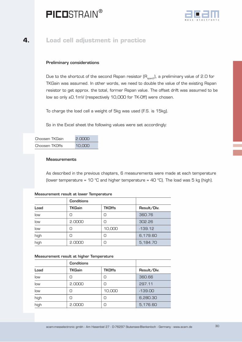
Preliminary considerations
Due to the shortcut of the second Rspan resistor (Rspan2), a preliminary value of 2.0 for
TKGain was assumed. In other words, we need to double the value of the existing Rspan
resistor to get approx. the total, former Rspan value. The offset drift was assumed to be
low so only ±0.1mV (respectively 10,000 for TK-Off) were chosen.
To charge the load cell a weight of 5kg was used (F.S. is 15kg).
So in the Excel sheet the following values were set accordingly:
Choosen TKGain 2.0000
Choosen TKOffs 10,000
Measurements
As described in the previous chapters, 6 measurements were made at each temperature
(lower temperature = 10 °C and higher temperature = 40 °C). The load was 5 kg (high).
Measurement result at lower Temperature
Conditions
Load TKGain TKOffs Result/Div.
low 0 0 360.76
low 2.0000 0 302.26
low 0 10,000 -139.12
high 0 0 6,179.60
high 2.0000 0 5,184.70
Measurement result at higher Temperature
Conditions
Load TKGain TKOffs Result/Div.
low 0 0 360.66
low 2.0000 0 297.11
low 0 10,000 -139.00
high 0 0 6,280.30
high 2.0000 0 5,176.60
4. Load cell adjustment in practice
acam-messelectronic gmbh - Am Hasenbiel 27 - D-76297 Stutensee-Blankenloch - Germany - www.acam.de 31
Results
Calculated Adjust Values for Load cell
PSØ21 TKGain: 1.91881 TKOffs: 73.34
PSØ8 TKGain: 1.91881 TKOffs: 7,334
The value of TKGain is with 1.91881 in the expected range and the value of TK-Off with
7,334 (73.34 ppm) is quite low and shows that the load cell was already good adjusted
previously.
Validation runs
In order to validate the results and see the compensation effect of the TK values, we
did a validation run. That means, two temperature drift curves of the offset drift (no load)
were taken with the following values:
a) first run with the preliminary values, that means without the calibration:
TKGain = 2.0 and TK-Off = 0
b) second run with the obtained proper TK-values:
TKGain = 1.91881 and TK-Off = 7,334
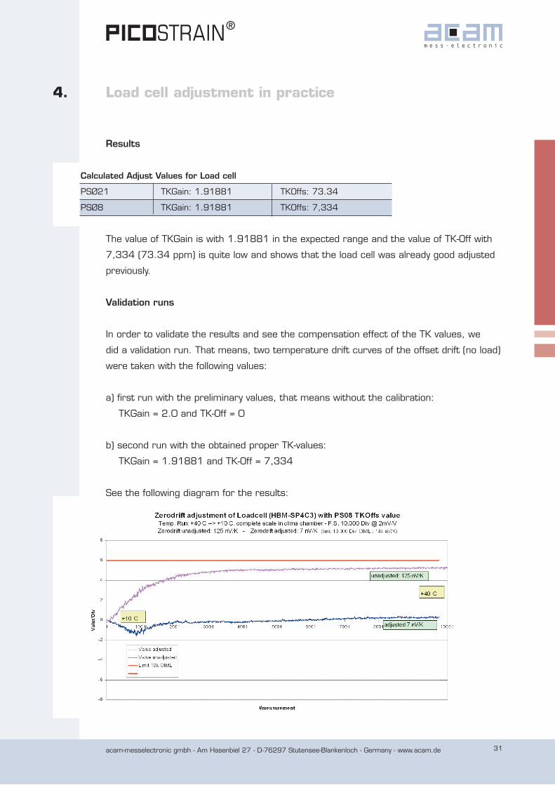
See the following diagram for the results:
4. Load cell adjustment in practice
acam-messelectronic gmbh - Am Hasenbiel 27 - D-76297 Stutensee-Blankenloch - Germany - www.acam.de 32
It can be seen that the result with the adjusted values is much better than unadjusted.
The red lines are indicating the limits for 10,000 OIML divisions (we took the limit values
for the whole scale, because load cell and electronics were in the temperature chamber).
The limit for the offset drift for 10,000 OIML divisions is 144 nV/K. Even if the compen-
sation is not applied, the curve is within the 10,000 OIML divisions limit (pink curve,
125 nV/K) which shows, that the load cell itself has already a good offset drift behavior.
Using the proper correction factors – that means the compensation of PICOSTRAIN is on
– the drift is extremely low with approx. 7 nV/K. This is much, much better than any
known existing specification and practically zero!
The limit for the gain drift for 10,000 OIML divisions is 5 ppm/K - again for the whole
scale. The measured gain drift of the load cell before compensation with TKGain = 2.0
was 52.2 ppm/K which is far beyond that value. But this significant overcompensation
effect is a result of the missing adjustment resistor for Rspan, which we removed in the
beginning. It is a normal procedure for load cell manufacturers to chose a Rspan with over-
compensation which is reduced then by the adjustment resistor to the proper value.
Using the correct TKGain value of 1.91828, the gain drift is reduced to –3.39 ppm/K.
This value is not so close to zero as it was the offset drift, but it is still good within the
limits of 10,000 OIML divisions.
So it can be shown, that both – the gain and the offset drift – could be improved signifi-
cantly by the use of the TK correction factors and generally speaking by the compensation
method of PSØ8/PSØ81. It was possible to prove, that this load cell in combination with
PSØ8/PSØ81 electronics is able to reach the 10,000 OIML division limits.
4.2 Applied on CZL-601 load cells
Setup
After testing the HBM load cell, we tested another 3 load cells of the type CZL-601. This
kind of load cell is delivered by acam with the PSØ8/PSØ81 evaluation kit. The load cell
comes already PICOSTRAIN-wired from the load cell manufacturer.
At the CZL-601-1 load cell we shortcutted the offset resistor to see the effect of this
compensation resistor. The other two load cells were not touched.
4. Load cell adjustment in practice
acam-messelectronic gmbh - Am Hasenbiel 27 - D-76297 Stutensee-Blankenloch - Germany - www.acam.de 33
Preliminary considerations
As the Rspan resistor is already roughly matched to the compensate the bridge, we
chosed TKGain as preliminary setting to 1.0. The offset drift was assumed in the range
of ±0.5 mV/V and therefore set to 50,000.
Choosen TKGain 1.0000
Choosen TKOffs 50,000
TKGain TK-Off
CZL-601-1 1.0143 61.978
CZL-601-2 1.0479 72.291
CZL-601-3 1.0215 5.884
So it can be seen, that the TKGain value is in all 3 cases approx. 1 and was chosen in
the correct range. The offset value is in 2 load cells higher than assumed, in one case
lower. With this values for TKGain and TK-Off we did the validation runs as previously with
the HBM cell. See the following results:
Validation runs
Again we did two temperature runs for each load cell, one with the unadjusted values
(TKGain = 1.0 and TK-Off = 0) and then afterwards with the calculated values shown in
the upper table. The results are as follows, first the values of the run without TK com-
pensation:
4. Load cell adjustment in practice
With this values the 6 measurements at each temperature (again 10 °C and 40 °C)
were done and written to the Excel sheet. We gained the following results from the
measurements:
Results
Before TKGain/TKOffs adjustment
Gaindrift ppm/K Offsetdrift nV/K
CZL-601-1 4.4 1,171.4
CZL-601-2 25.2 1,434.5
CZL-601-3 11.2 107.8
OIML 10,000 div. Limits (whole scale)
Offset drift: 144 nV/K
Gain drift: 5 ppm/K
acam-messelectronic gmbh - Am Hasenbiel 27 - D-76297 Stutensee-Blankenloch - Germany - www.acam.de 34
CZL-601-1:
As we shortcutted the offset compensation resistor at this load cell, the offset drift was
quite high with 1,171 nV/K and far out of the OIML specificatiton. The gain drift was
very good with 4.4 ppm/K.
CZL-601-2:
This load cell wasn’t modified by acam. It showed very bad temperature drift behavior in
both, the gain and offset drift and far beyond the OIML limits. It seems, that no compen-
sation was done at all from the load cell manufacturer.
CZL-601-3:
This load cell wasn’t modified by acam. It showed quite good behavior in both, the gain
and offset drift. The values are within the 10,000 OIML divisions specification.
The following table shows the values with the proper TKGain and TK-off values set (active
compensation):
4. Load cell adjustment in practice
After TKGain/TKOffs adjustment
Gaindrift ppm/K Offsetdrift nV/K
CZL-601-1 0.7 34.8
CZL-601-2 2.2 -33.4
CZL-601-3 -1.2 36.0
With active PICOSTRAIN compensation ALL load cells meet the 10,000 OIML divisions
specification!
The offset drift of all load cells are between 30 and 40 nV/K. This is a value which is
normally only reached with today’s best C6 load cells. With the PICOSTRAIN compensation
method it was possible to bring ordinary C3 load cells in this range – and this although
we had 2 load cells with very bad offset drift behavior before (in one we shortcutted the
offset resistor, the other one was obviously not adjusted by the manufacturer at all).
The gain drift was less than 3 ppm/K at all load cell after the adjustment. We here at
acam do not know any load cell which is specified with such low values.
acam-messelectronic gmbh - Am Hasenbiel 27 - D-76297 Stutensee-Blankenloch - Germany - www.acam.de 35
4.3 Conclusion
The performed tests prove the theoretical explanations in this sheet. We showed, that
the temperature compensation of PICOSTRAIN for load cells works as expected and that
the results are really impressive.
The quality load cell from HBM was before the compensation already in a good range
regarding the offset drift, the gain drift was not representative as we removed the Rspan
adjustment resistor. With the PICOSTRAIN compensation we got impressive results
regarding the offset drift (7nV/K, which is practically zero) and brought the gain drift into
the 10,000 OIML divisions specification. This corresponds to an improvement of almost
18 times!
The tests with the three ordinary C3 load cells were even more impressive. In spite of a
bad starting position (no compensation at all and removed offset resistor) we brought
them with PICOSTRAIN compensation to an offset drift behavior which only very good C6
load cells have (the worst load cell was improved by factor 44!) and in regards of the gain
drift to absolute fantastic values (<3 ppm/K), which is an improvement by factor 6 to
11, depending on which load cell we are looking. With active compensation all 3 load
cells are deeply within the 10,000 OIML divisions specification!
As demonstrated the PICOSTRAIN compensation works very well and offers possibilities
not known nowadays. We can imagine that this method will lead to increased quality in
the area of load cell production. The acam team will be glad to assist you in load cell
adjusting with PICOSTRAIN.
acam headquarters, Stutensee, October 2008 and February 2010
4. Load cell adjustment in practice