Embed Size (px)
Citation preview
How to Design Battery-Assisted Photovoltaic Switched-Inductor CMOS Charger–Supplies
Rajiv Damodaran Prabha, Graduate Student Member, IEEE, and Gabriel A. Rincón-Mora, Fellow, IEEE Georgia Institute of Technology, Atlanta, Georgia 30332 U.S.A.
[email protected] and [email protected]
Abstract—Wireless microsensors can sense and share data that can save lives, energy, and money. Recharging or replacing thousands of tiny, easily exhaustible batteries, however, is too costly. Fortunately, photovoltaic (PV) cells can generate 100× more power from sunlight than other transducers can from motion, heat, or radiation. But since PV cells cannot supply the milliwatts that microsystems can at times require, this paper shows how to design battery-assisted PV-sourced CMOS charger–supplies that supply PV power to the system, excess PV power to the battery, and battery power to the system when PV power is insufficient. The design process proposed accounts for power losses and silicon area. This way, simulations show that 10% of losses are from switches when inductor resistance RESR is 2.2 Ω and silicon area can be 80% smaller when RESR is 5.5 Ω.
Index Terms—Charger, harvester, light energy, photovoltaic (PV), power supply, switched inductor, microsensor, microsystem.
I. BATTERY-ASSISTED MICROSYSTEMS Microsensors can add life-, energy-, and cost-saving intelligence to homes, hospitals, factories, and cities [1]–[6]. But since tiny batteries deplete easily, life times can be short and recharge cycles frequent. And the cost of recharging or replacing thousands of nodes is excessive. Fortunately, ambient energy is often abundant, and as a result, able to repeatedly replenish the energy that the batteries lose.
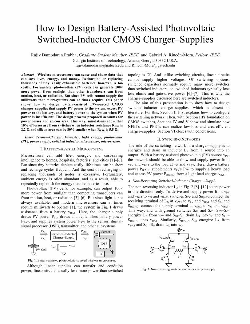
Photovoltaic (PV) cells, for example, can output 100× more power from sunlight than competing transducers can from motion, heat, or radiation [3]–[6]. But since light is not always available, and modern microsensors can at times require milliwatts to operate [1], the system in Fig. 1 draws assistance from a battery vBAT. Here, the charger–supply draws PV power PPV, draws and replenishes battery power PBAT, and supplies system power PSYS to the sensor, digital-signal processor (DSP), transmitter, and other subsystems.
Fig. 1. Battery-assisted photovoltaic-sourced wireless microsensor.
Although linear supplies can transfer and condition power, linear circuits usually lose more power than switched
topologies [2]. And unlike switching circuits, linear circuits cannot supply higher voltages. Of switching options, switched capacitors normally require many more switches than switched inductors, so switched inductors typically lose less ohmic and gate-drive power [6]–[7]. This is why the charger–supplies discussed here are switched inductors.
The aim of this presentation is to show how to design switched-inductor charger–supplies, which is absent in literature. For this, Section II first explains how to configure the switching network. Then, with Section III's foundation on CMOS switches, Sections IV and V show and simulate how NFETs and PFETs can realize low-loss and area-efficient charger–supplies. Section VI closes with conclusions.
II. SWITCHING NETWORKS The role of the switching network in a charger–supply is to energize and drain an inductor LX from a source into an output. With a battery-assisted photovoltaic (PV) source vPV, the network should be able to draw and supply power from vPV and vBAT to the load at vO and vBAT. Here, drawn battery power PB(AID) supplements vPV's PPV to supply a heavy load and excess PV power PB(CHG) from a light load charges vBAT.
A. Non-Reversing Switched-Inductor Charger–Supply The non-reversing inductor LX in Fig. 2 [8]–[12] steers power in one direction only. To derive and supply power from vPV and vBAT to vO and vBAT, switches SPV and SB(AID) connect the receiving terminal of LX at vSW1 to vPV and vBAT and SO and SB(CHG) connect the supply terminal at vSW2 to vO and vBAT. This way, and with ground switches SG1 and SG2, SPV–SG2 energize LX from vPV and SG1–SO drain LX into vO and SG1–SB(CHG) into vBAT. Similarly, SB(AID)–SG2 energize LX from vBAT and SG1–SO drain LX into vO.
Fig. 2. Non-reversing switched-inductor charger–supply.
TX
vBAT
PV Cell
vPV
PPV
vO
PSYS
PBAT
Charger–SupplySwitched-Inductor
Sensor
DSP
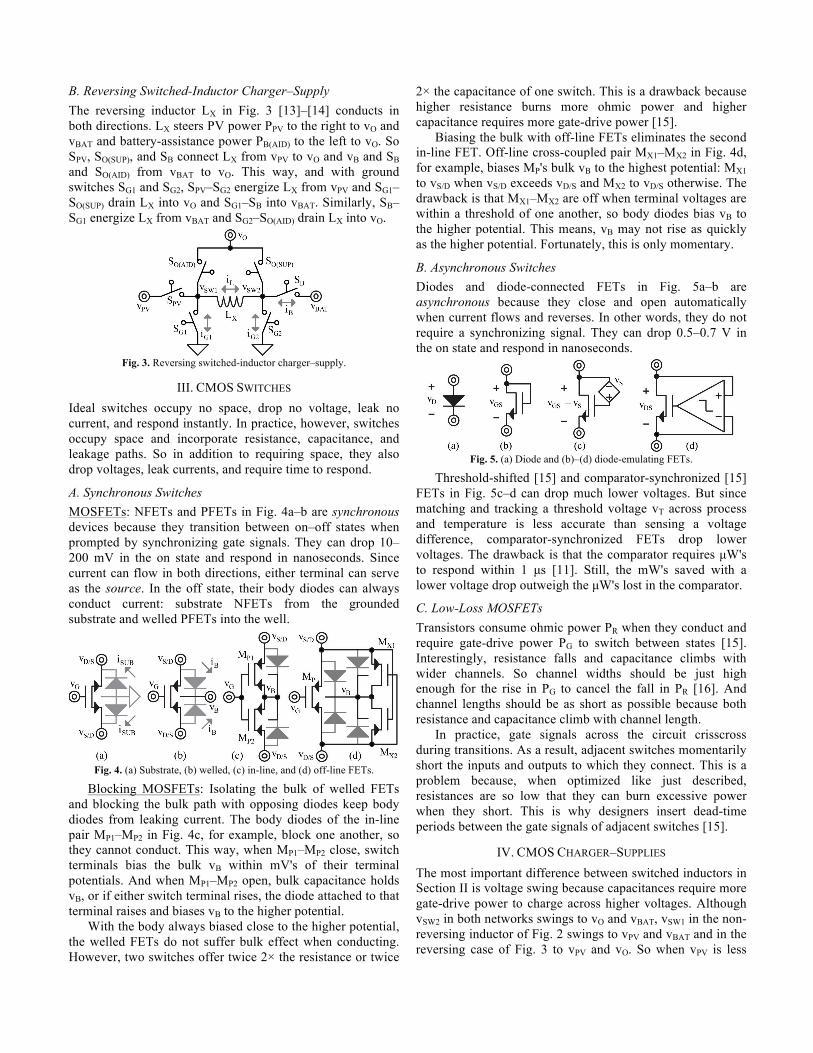
B. Reversing Switched-Inductor Charger–Supply The reversing inductor LX in Fig. 3 [13]–[14] conducts in both directions. LX steers PV power PPV to the right to vO and vBAT and battery-assistance power PB(AID) to the left to vO. So SPV, SO(SUP), and SB connect LX from vPV to vO and vB and SB and SO(AID) from vBAT to vO. This way, and with ground switches SG1 and SG2, SPV–SG2 energize LX from vPV and SG1–SO(SUP) drain LX into vO and SG1–SB into vBAT. Similarly, SB–SG1 energize LX from vBAT and SG2–SO(AID) drain LX into vO.
Fig. 3. Reversing switched-inductor charger–supply.
III. CMOS SWITCHES Ideal switches occupy no space, drop no voltage, leak no current, and respond instantly. In practice, however, switches occupy space and incorporate resistance, capacitance, and leakage paths. So in addition to requiring space, they also drop voltages, leak currents, and require time to respond.
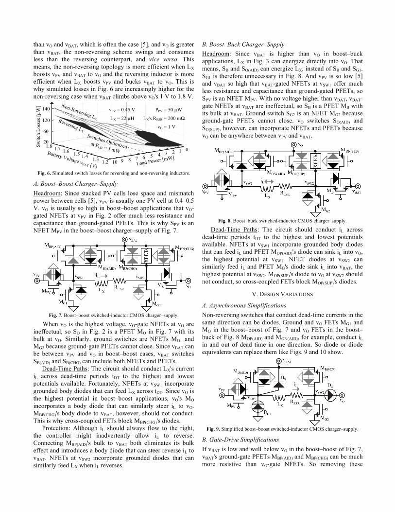
A. Synchronous Switches MOSFETs: NFETs and PFETs in Fig. 4a–b are synchronous devices because they transition between on–off states when prompted by synchronizing gate signals. They can drop 10–200 mV in the on state and respond in nanoseconds. Since current can flow in both directions, either terminal can serve as the source. In the off state, their body diodes can always conduct current: substrate NFETs from the grounded substrate and welled PFETs into the well.
Fig. 4. (a) Substrate, (b) welled, (c) in-line, and (d) off-line FETs.
Blocking MOSFETs: Isolating the bulk of welled FETs and blocking the bulk path with opposing diodes keep body diodes from leaking current. The body diodes of the in-line pair MP1–MP2 in Fig. 4c, for example, block one another, so they cannot conduct. This way, when MP1–MP2 close, switch terminals bias the bulk vB within mV's of their terminal potentials. And when MP1–MP2 open, bulk capacitance holds vB, or if either switch terminal rises, the diode attached to that terminal raises and biases vB to the higher potential.
With the body always biased close to the higher potential, the welled FETs do not suffer bulk effect when conducting. However, two switches offer twice 2× the resistance or twice
2× the capacitance of one switch. This is a drawback because higher resistance burns more ohmic power and higher capacitance requires more gate-drive power [15].
Biasing the bulk with off-line FETs eliminates the second in-line FET. Off-line cross-coupled pair MX1–MX2 in Fig. 4d, for example, biases MP's bulk vB to the highest potential: MX1 to vS/D when vS/D exceeds vD/S and MX2 to vD/S otherwise. The drawback is that MX1–MX2 are off when terminal voltages are within a threshold of one another, so body diodes bias vB to the higher potential. This means, vB may not rise as quickly as the higher potential. Fortunately, this is only momentary.
B. Asynchronous Switches Diodes and diode-connected FETs in Fig. 5a–b are asynchronous because they close and open automatically when current flows and reverses. In other words, they do not require a synchronizing signal. They can drop 0.5–0.7 V in the on state and respond in nanoseconds.
Fig. 5. (a) Diode and (b)–(d) diode-emulating FETs.
Threshold-shifted [15] and comparator-synchronized [15] FETs in Fig. 5c–d can drop much lower voltages. But since matching and tracking a threshold voltage vT across process and temperature is less accurate than sensing a voltage difference, comparator-synchronized FETs drop lower voltages. The drawback is that the comparator requires µW's to respond within 1 µs [11]. Still, the mW's saved with a lower voltage drop outweigh the µW's lost in the comparator.
C. Low-Loss MOSFETs Transistors consume ohmic power PR when they conduct and require gate-drive power PG to switch between states [15]. Interestingly, resistance falls and capacitance climbs with wider channels. So channel widths should be just high enough for the rise in PG to cancel the fall in PR [16]. And channel lengths should be as short as possible because both resistance and capacitance climb with channel length.
In practice, gate signals across the circuit crisscross during transitions. As a result, adjacent switches momentarily short the inputs and outputs to which they connect. This is a problem because, when optimized like just described, resistances are so low that they can burn excessive power when they short. This is why designers insert dead-time periods between the gate signals of adjacent switches [15].
IV. CMOS CHARGER–SUPPLIES The most important difference between switched inductors in Section II is voltage swing because capacitances require more gate-drive power to charge across higher voltages. Although vSW2 in both networks swings to vO and vBAT, vSW1 in the non-reversing inductor of Fig. 2 swings to vPV and vBAT and in the reversing case of Fig. 3 to vPV and vO. So when vPV is less
than vO and vBAT, which is often the case [5], and vO is greater than vBAT, the non-reversing scheme swings and consumes less than the reversing counterpart, and vice versa. This means, the non-reversing topology is more efficient when LX boosts vPV and vBAT to vO and the reversing inductor is more efficient when LX boosts vPV and bucks vBAT to vO. This is why simulated losses in Fig. 6 are increasingly higher for the non-reversing case when vBAT climbs above vO's 1 V to 1.8 V.
Fig. 6. Simulated switch losses for reversing and non-reversing inductors.
A. Boost–Boost Charger–Supply Headroom: Since stacked PV cells lose space and mismatch power between cells [5], vPV is usually one PV cell at 0.4–0.5 V. vO is usually so high in boost–boost applications that vO-gated NFETs at vPV in Fig. 2 offer much less resistance and capacitance than ground-gated PFETs. This is why SPV is an NFET MPV in the boost–boost charger–supply of Fig. 7.
Fig. 7. Boost–boost switched-inductor CMOS charger–supply.
When vO is the highest voltage, vO-gate NFETs at vO are ineffectual, so SO in Fig. 2 is a PFET MO in Fig. 7 with its bulk at vO. Similarly, ground switches are NFETs MG1 and MG2 because ground-gate PFETs cannot close. Since vBAT can be between vPV and vO in boost–boost cases, vBAT switches SB(AID) and SB(CHG) can include both NFETs and PFETs.
Dead-Time Paths: The circuit should conduct LX's current iL across dead-time periods tDT to the highest and lowest potentials available. Fortunately, NFETs at vSW1 incorporate grounded body diodes that can feed LX across tDT. Since vO is the highest potential in boost–boost applications, vO's MO incorporates a body diode that can similarly steer iL to vO. MBP(CHG)'s body diode to vBAT, however, should not conduct. This is why cross-coupled FETs block MBP(CHG)'s diodes.
Protection: Although iL should always flow to the right, the controller might inadvertently allow iL to reverse. Connecting MBP(AID)'s bulk to vBAT both eliminates its bulk effect and introduces a body diode that can steer reverse iL to vBAT. NFETs at vSW2 incorporate grounded diodes that can similarly feed LX when iL reverses.
B. Boost–Buck Charger–Supply Headroom: Since vBAT is higher than vO in boost–buck applications, LX in Fig. 3 can energize directly into vO. That means, SB and SO(AID) can energize LX, instead of SB and SG1. SG1 is therefore unnecessary in Fig. 8. And vPV is so low [5] and vBAT so high that vBAT-gated NFETs at vSW1 offer much less resistance and capacitance than ground-gated PFETs, so SPV is an NFET MPV. With no voltage higher than vBAT, vBAT-gate NFETs at vBAT are ineffectual, so SB is a PFET MB with its bulk at vBAT. Ground switch SG2 is an NFET MG2 because ground-gate PFETs cannot close. vO switches SO(AID) and SO(SUP), however, can incorporate NFETs and PFETs because vO can be anywhere between vPV and vBAT.
Fig. 8. Boost–buck switched-inductor CMOS charger–supply.
Dead-Time Paths: The circuit should conduct iL across dead-time periods tDT to the highest and lowest potentials available. NFETs at vSW1 incorporate grounded body diodes that can feed iL and PFET MOP(AID)'s diode can sink iL into vO, the highest potential at vSW1. NFET diodes at vSW2 can similarly feed iL and PFET MB's diode sink iL into vBAT, the highest potential at vSW2. MOP(SUP)'s diode to vO at vSW2 should not conduct, so cross-coupled FETs block MOP(SUP)'s diodes.
V. DESIGN VARIATIONS
A. Asynchronous Simplifications Non-reversing switches that conduct dead-time currents in the same direction can be diodes. Ground and vO FETs MG1 and MO in the boost–boost of Fig. 7 and vO FETs in the boost–buck of Fig. 8 MOP(AID) and MON(AID), for example, conduct iL in and out of dead time in one direction. So diode or diode equivalents can replace them like Figs. 9 and 10 show.
Fig. 9. Simplified boost–boost switched-inductor CMOS charger–supply.
B. Gate-Drive Simplifications If vBAT is low and well below vO in the boost–boost of Fig. 7, vBAT's ground-gate PFETs MBP(AID) and MBP(CHG) can be much more resistive than vO-gate NFETs. So removing these
201.7 1.6
1.4 1.3 1.2
2468Load Power [mW]910
Battery Voltage vBAT [V]
1.8
140
120
60
Switc
h Lo
sses
[µW
]
1.5
Non-Reversing LXReversing LX
LX's RESR = 200 mΩ
PPV = 50 µW
vO = 1 V
Switches Optimizedat PLD = 5 mW 7
1350
vPV = 0.45 V
LX = 22 µH
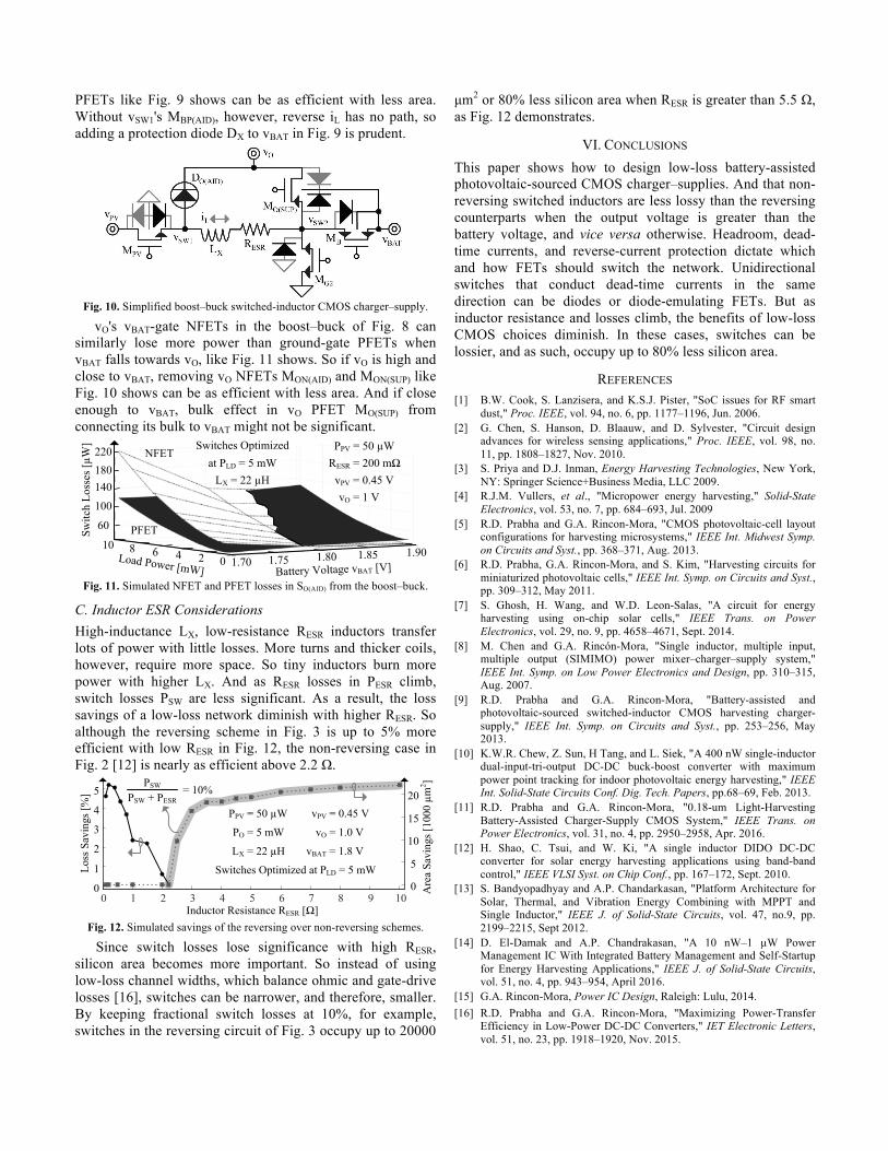
PFETs like Fig. 9 shows can be as efficient with less area. Without vSW1's MBP(AID), however, reverse iL has no path, so adding a protection diode DX to vBAT in Fig. 9 is prudent.
Fig. 10. Simplified boost–buck switched-inductor CMOS charger–supply.
vO's vBAT-gate NFETs in the boost–buck of Fig. 8 can similarly lose more power than ground-gate PFETs when vBAT falls towards vO, like Fig. 11 shows. So if vO is high and close to vBAT, removing vO NFETs MON(AID) and MON(SUP) like Fig. 10 shows can be as efficient with less area. And if close enough to vBAT, bulk effect in vO PFET MO(SUP) from connecting its bulk to vBAT might not be significant.
Fig. 11. Simulated NFET and PFET losses in SO(AID) from the boost–buck.
C. Inductor ESR Considerations High-inductance LX, low-resistance RESR inductors transfer lots of power with little losses. More turns and thicker coils, however, require more space. So tiny inductors burn more power with higher LX. And as RESR losses in PESR climb, switch losses PSW are less significant. As a result, the loss savings of a low-loss network diminish with higher RESR. So although the reversing scheme in Fig. 3 is up to 5% more efficient with low RESR in Fig. 12, the non-reversing case in Fig. 2 [12] is nearly as efficient above 2.2 Ω.
Fig. 12. Simulated savings of the reversing over non-reversing schemes.
Since switch losses lose significance with high RESR, silicon area becomes more important. So instead of using low-loss channel widths, which balance ohmic and gate-drive losses [16], switches can be narrower, and therefore, smaller. By keeping fractional switch losses at 10%, for example, switches in the reversing circuit of Fig. 3 occupy up to 20000
µm2 or 80% less silicon area when RESR is greater than 5.5 Ω, as Fig. 12 demonstrates.
VI. CONCLUSIONS This paper shows how to design low-loss battery-assisted photovoltaic-sourced CMOS charger–supplies. And that non-reversing switched inductors are less lossy than the reversing counterparts when the output voltage is greater than the battery voltage, and vice versa otherwise. Headroom, dead-time currents, and reverse-current protection dictate which and how FETs should switch the network. Unidirectional switches that conduct dead-time currents in the same direction can be diodes or diode-emulating FETs. But as inductor resistance and losses climb, the benefits of low-loss CMOS choices diminish. In these cases, switches can be lossier, and as such, occupy up to 80% less silicon area.
REFERENCES [1] B.W. Cook, S. Lanzisera, and K.S.J. Pister, "SoC issues for RF smart
dust," Proc. IEEE, vol. 94, no. 6, pp. 1177–1196, Jun. 2006. [2] G. Chen, S. Hanson, D. Blaauw, and D. Sylvester, "Circuit design
advances for wireless sensing applications," Proc. IEEE, vol. 98, no. 11, pp. 1808–1827, Nov. 2010.
[3] S. Priya and D.J. Inman, Energy Harvesting Technologies, New York, NY: Springer Science+Business Media, LLC 2009.
[4] R.J.M. Vullers, et al., "Micropower energy harvesting," Solid-State Electronics, vol. 53, no. 7, pp. 684–693, Jul. 2009
[5] R.D. Prabha and G.A. Rincon-Mora, "CMOS photovoltaic-cell layout configurations for harvesting microsystems," IEEE Int. Midwest Symp. on Circuits and Syst., pp. 368–371, Aug. 2013.
[6] R.D. Prabha, G.A. Rincon-Mora, and S. Kim, "Harvesting circuits for miniaturized photovoltaic cells," IEEE Int. Symp. on Circuits and Syst., pp. 309–312, May 2011.
[7] S. Ghosh, H. Wang, and W.D. Leon-Salas, "A circuit for energy harvesting using on-chip solar cells," IEEE Trans. on Power Electronics, vol. 29, no. 9, pp. 4658–4671, Sept. 2014.
[8] M. Chen and G.A. Rincón-Mora, "Single inductor, multiple input, multiple output (SIMIMO) power mixer–charger–supply system," IEEE Int. Symp. on Low Power Electronics and Design, pp. 310–315, Aug. 2007.
[9] R.D. Prabha and G.A. Rincon-Mora, "Battery-assisted and photovoltaic-sourced switched-inductor CMOS harvesting charger-supply," IEEE Int. Symp. on Circuits and Syst., pp. 253–256, May 2013.
[10] K.W.R. Chew, Z. Sun, H Tang, and L. Siek, "A 400 nW single-inductor dual-input-tri-output DC-DC buck-boost converter with maximum power point tracking for indoor photovoltaic energy harvesting," IEEE Int. Solid-State Circuits Conf. Dig. Tech. Papers, pp.68–69, Feb. 2013.
[11] R.D. Prabha and G.A. Rincon-Mora, "0.18-um Light-Harvesting Battery-Assisted Charger-Supply CMOS System," IEEE Trans. on Power Electronics, vol. 31, no. 4, pp. 2950–2958, Apr. 2016.
[12] H. Shao, C. Tsui, and W. Ki, "A single inductor DIDO DC-DC converter for solar energy harvesting applications using band-band control," IEEE VLSI Syst. on Chip Conf., pp. 167–172, Sept. 2010.
[13] S. Bandyopadhyay and A.P. Chandarkasan, "Platform Architecture for Solar, Thermal, and Vibration Energy Combining with MPPT and Single Inductor," IEEE J. of Solid-State Circuits, vol. 47, no.9, pp. 2199–2215, Sept 2012.
[14] D. El-Damak and A.P. Chandrakasan, "A 10 nW–1 µW Power Management IC With Integrated Battery Management and Self-Startup for Energy Harvesting Applications," IEEE J. of Solid-State Circuits, vol. 51, no. 4, pp. 943–954, April 2016.
[15] G.A. Rincon-Mora, Power IC Design, Raleigh: Lulu, 2014. [16] R.D. Prabha and G.A. Rincon-Mora, "Maximizing Power-Transfer
Efficiency in Low-Power DC-DC Converters," IET Electronic Letters, vol. 51, no. 23, pp. 1918–1920, Nov. 2015.
220180140
100
60
Switc
h Lo
sses
[µW
]
10 8 6 4 2 1.80 1.90Load Power [mW] Battery Voltage vBAT [V]
NFET
PFET
1.75 1.850 1.70
RESR = 200 mΩPPV = 50 µW
vPV = 0.45 VvO = 1 V
Switches Optimized
LX = 22 µHat PLD = 5 mW
00 1 2 3 4 5 6 7 8 9 10
0
5
10
15
20
Loss
Sav
ings
[%]
Are
a Sa
ving
s [10
00 µ
m2 ]
Inductor Resistance RESR [Ω]
Switches Optimized at PLD = 5 mW
PSW
PSW + PESR= 10%
1
2
3
4
5
PPV = 50 µW vPV = 0.45 V
PO = 5 mW vO = 1.0 V
vBAT = 1.8 VLX = 22 µH