Embed Size (px)
Citation preview
How can we Design and Build the Next Generation of MEMS-Based Products? Presented by Coventor and X-FABDecember 6, 2017
Moderator: Heidi Hoffman, Sr. Director, SEMI-MSIG
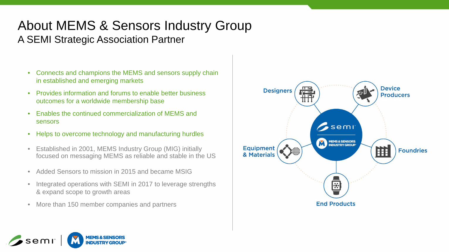
• Connects and champions the MEMS and sensors supply chain in established and emerging markets
• Provides information and forums to enable better business outcomes for a worldwide membership base
• Enables the continued commercialization of MEMS and sensors
• Helps to overcome technology and manufacturing hurdles
• Established in 2001, MEMS Industry Group (MIG) initially focused on messaging MEMS as reliable and stable in the US
• Added Sensors to mission in 2015 and became MSIG
• Integrated operations with SEMI in 2017 to leverage strengths & expand scope to growth areas
• More than 150 member companies and partners
About MEMS & Sensors Industry GroupA SEMI Strategic Association Partner
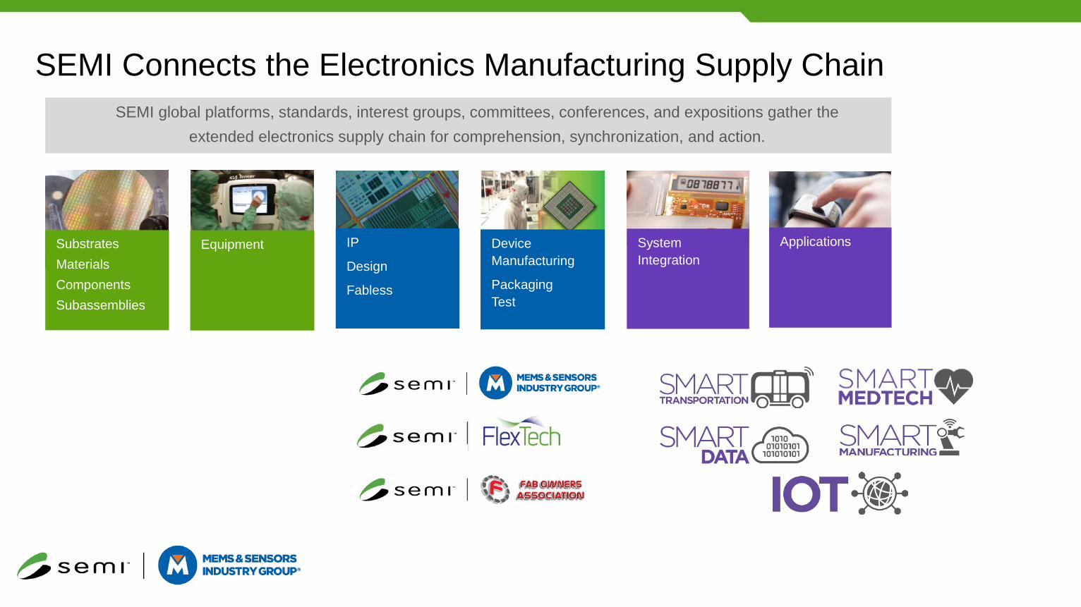
SEMI Connects the Electronics Manufacturing Supply Chain
SubstratesMaterialsComponentsSubassemblies
Equipment ApplicationsSystem Integration
Device Manufacturing
PackagingTest
IP
Design
Fabless
SEMI global platforms, standards, interest groups, committees, conferences, and expositions gather the extended electronics supply chain for comprehension, synchronization, and action.

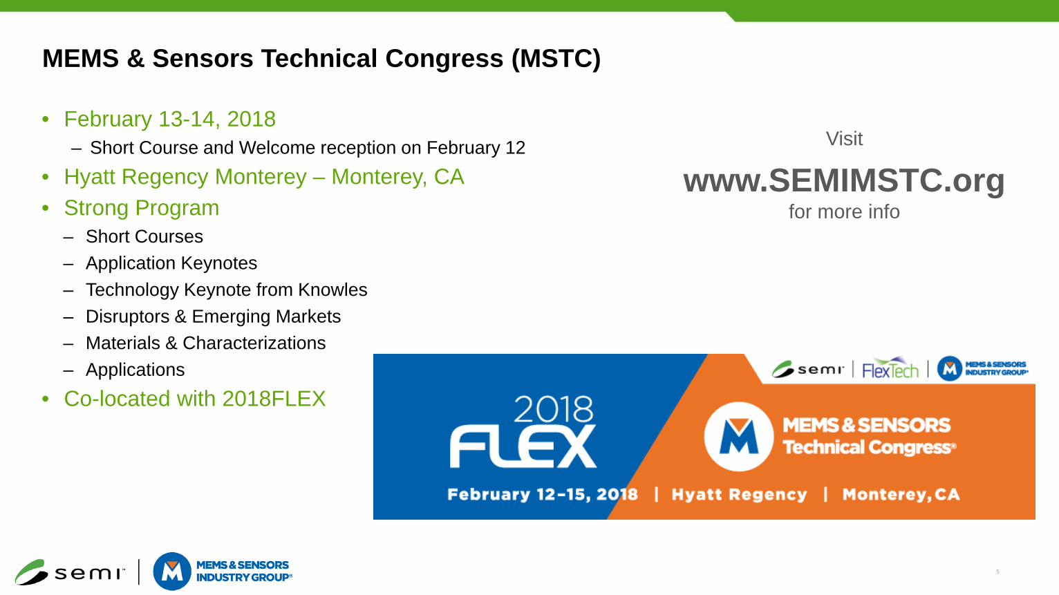
MEMS & Sensors Technical Congress (MSTC)
• February 13-14, 2018– Short Course and Welcome reception on February 12
• Hyatt Regency Monterey – Monterey, CA• Strong Program
– Short Courses– Application Keynotes– Technology Keynote from Knowles– Disruptors & Emerging Markets– Materials & Characterizations– Applications
• Co-located with 2018FLEX
Visit
www.SEMIMSTC.orgfor more info
5
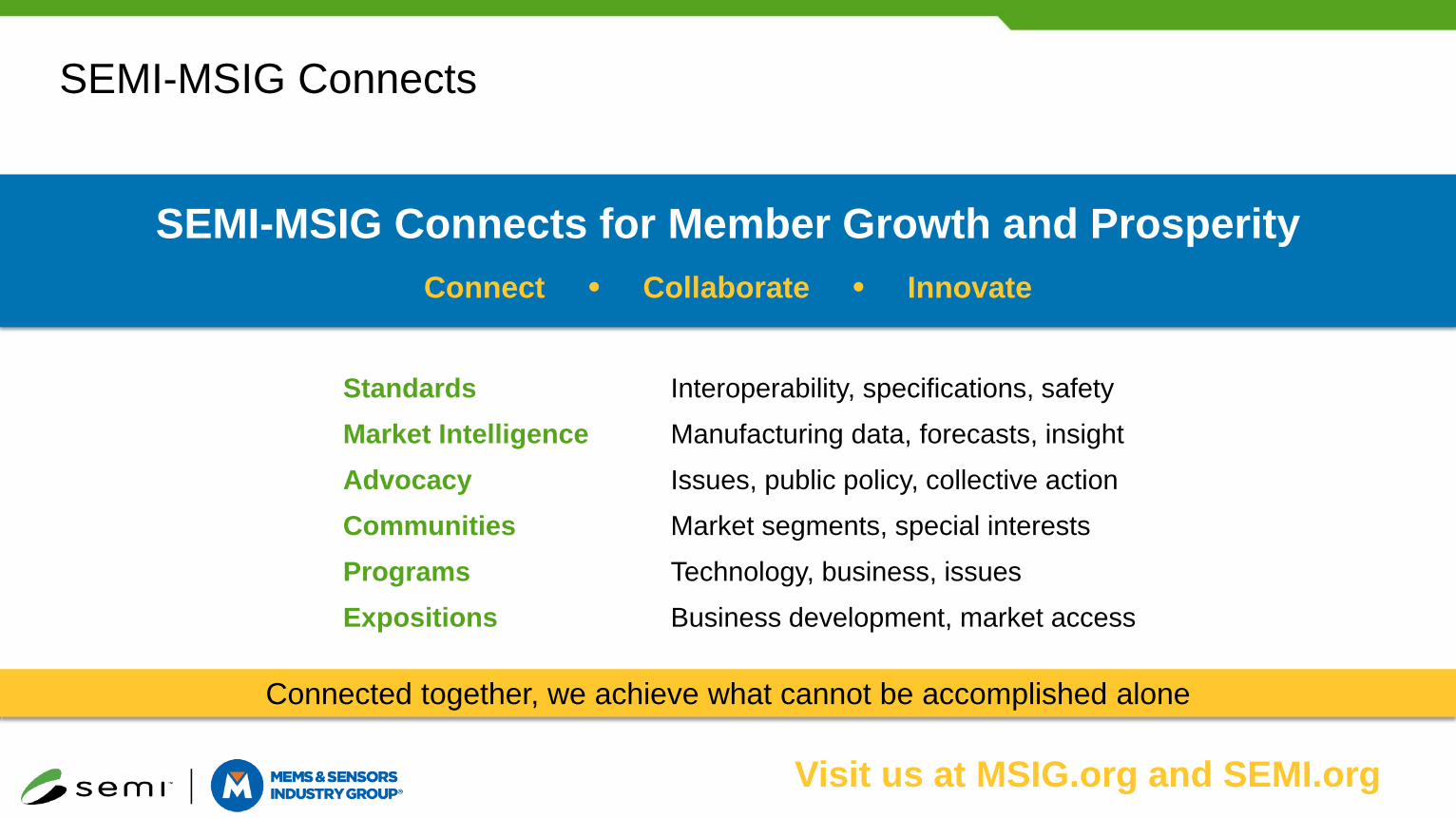
SEMI-MSIG Connects
SEMI-MSIG Connects for Member Growth and ProsperityConnect Collaborate Innovate
Standards Interoperability, specifications, safetyMarket Intelligence Manufacturing data, forecasts, insightAdvocacy Issues, public policy, collective actionCommunities Market segments, special interestsPrograms Technology, business, issuesExpositions Business development, market access
Connected together, we achieve what cannot be accomplished alone
Visit us at MSIG.org and SEMI.org
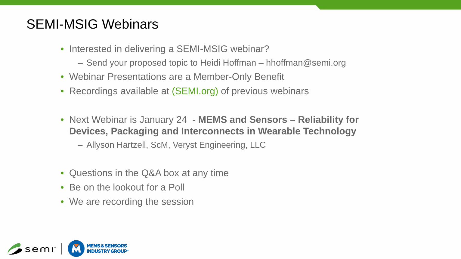
SEMI-MSIG Webinars
• Interested in delivering a SEMI-MSIG webinar?– Send your proposed topic to Heidi Hoffman – [email protected]
• Webinar Presentations are a Member-Only Benefit• Recordings available at (SEMI.org) of previous webinars
• Next Webinar is January 24 - MEMS and Sensors – Reliability for Devices, Packaging and Interconnects in Wearable Technology
– Allyson Hartzell, ScM, Veryst Engineering, LLC
• Questions in the Q&A box at any time• Be on the lookout for a Poll• We are recording the session
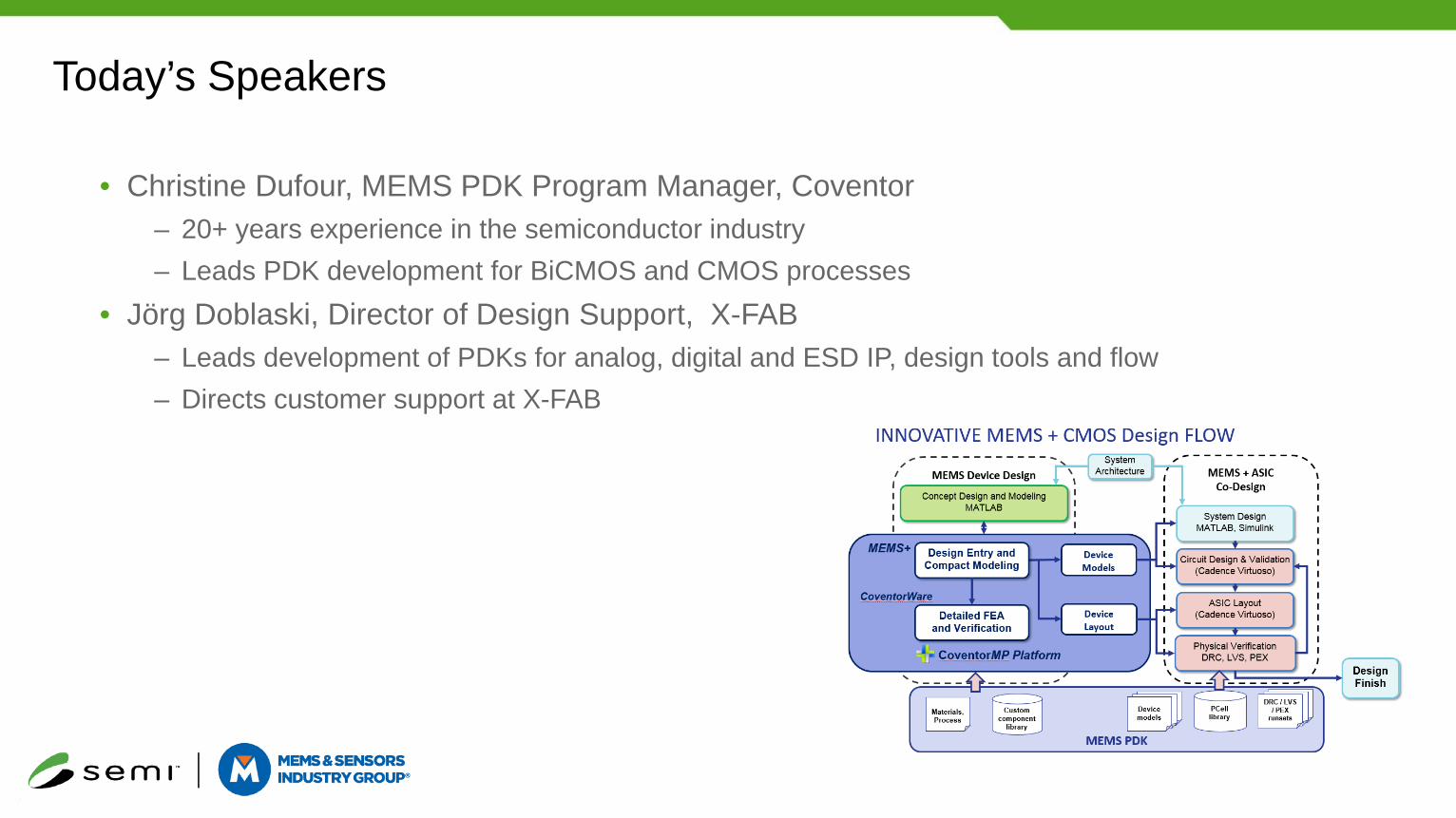
Today’s Speakers
• Christine Dufour, MEMS PDK Program Manager, Coventor– 20+ years experience in the semiconductor industry– Leads PDK development for BiCMOS and CMOS processes
• Jörg Doblaski, Director of Design Support, X-FAB– Leads development of PDKs for analog, digital and ESD IP, design tools and flow– Directs customer support at X-FAB
How can we Design and Build the Next Generation of MEMS-Based Products?Christine Dufour (Coventor), Joerg Doblaski (X-FAB)
Outline
• About Coventor and X-FAB• MEMS design challenges and solutions• Coventor MEMS+ PDK and Design Flow• Cadence Virtuoso PDK for X-FAB XMB10 process• Summary and Outlook
10
About Coventor and X-FAB
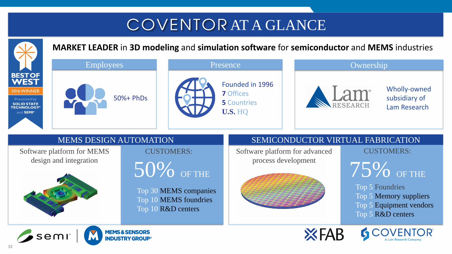
MARKET LEADER in 3D modeling and simulation software for semiconductor and MEMS industries
Founded in 19967 Offices5 CountriesU.S. HQ
ProfitablePrivately
HeldWholly-owned subsidiary of Lam Research
AT A GLANCE
50%+ PhDs
Employees Presence Ownership
MEMS DESIGN AUTOMATION SEMICONDUCTOR VIRTUAL FABRICATIONSoftware platform for MEMS
design and integrationCUSTOMERS:
Top 30 MEMS companiesTop 10 MEMS foundriesTop 10 R&D centers
50% OF THE
Software platform for advanced process development
CUSTOMERS:
75% OF THETop 5 FoundriesTop 5 Memory suppliersTop 5 Equipment vendorsTop 5 R&D centers
12

Coventor MEMS Design Automation Tools
MEMS+®CoventorWare®• Gold standard accuracy for MEMS physics:
Electrostatics, coupled electro-mechanics, …
• Faster time to solution: 100X faster simulations for concept exploration and design optimization
• Fit MEMS into system and CMOS design flow:Integration with MATLAB and Cadence
Cadence Virtuoso®
MATLAB Simulink®
CoventorMP® MEMS Design Automation Platform
Device Design System Optimization
Supports PDK Design Automation
13
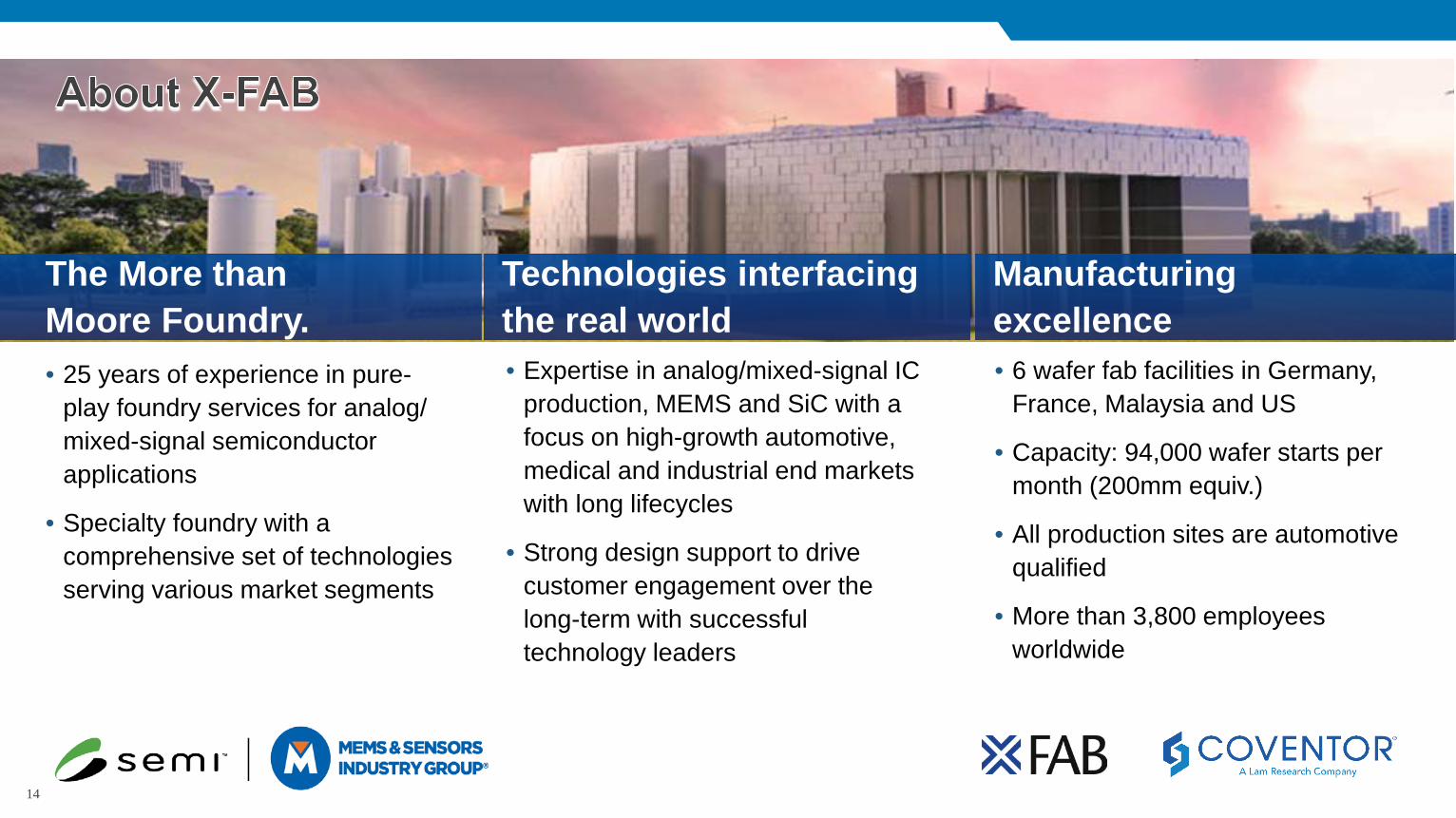
The More than Moore Foundry.• 25 years of experience in pure-
play foundry services for analog/mixed-signal semiconductor applications
• Specialty foundry with a comprehensive set of technologies serving various market segments
Manufacturing excellence• 6 wafer fab facilities in Germany,
France, Malaysia and US
• Capacity: 94,000 wafer starts per month (200mm equiv.)
• All production sites are automotive qualified
• More than 3,800 employees worldwide
Technologies interfacing the real world• Expertise in analog/mixed-signal IC
production, MEMS and SiC with a focus on high-growth automotive, medical and industrial end markets with long lifecycles
• Strong design support to drive customer engagement over the long-term with successful technology leaders
14
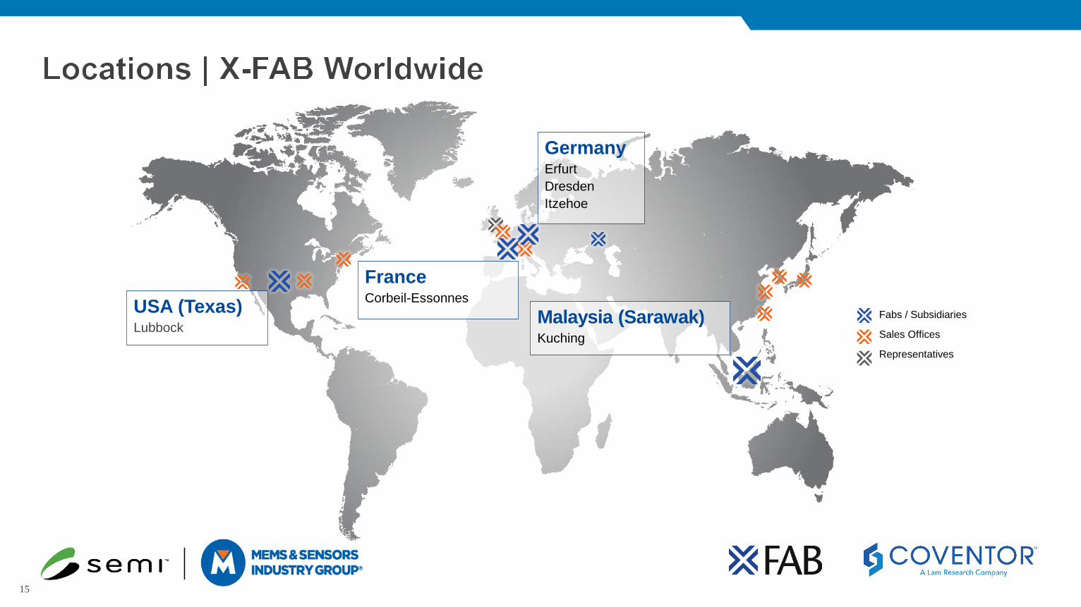
Fabs / Subsidiaries
Sales Offices
Representatives
Malaysia (Sarawak)Kuching
GermanyErfurtDresdenItzehoe
USA (Texas)Lubbock
FranceCorbeil-Essonnes-
15
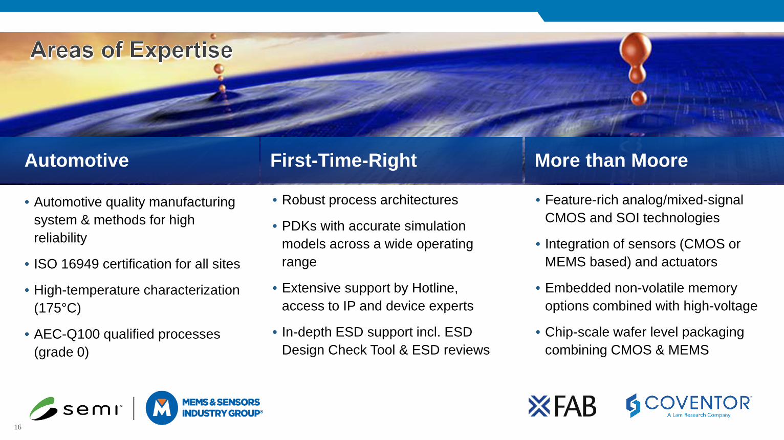
Automotive
• Automotive quality manufacturing system & methods for high reliability
• ISO 16949 certification for all sites
• High-temperature characterization (175°C)
• AEC-Q100 qualified processes (grade 0)
More than Moore
• Feature-rich analog/mixed-signal CMOS and SOI technologies
• Integration of sensors (CMOS or MEMS based) and actuators
• Embedded non-volatile memory options combined with high-voltage
• Chip-scale wafer level packaging combining CMOS & MEMS
First-Time-Right
• Robust process architectures
• PDKs with accurate simulation models across a wide operating range
• Extensive support by Hotline, access to IP and device experts
• In-depth ESD support incl. ESD Design Check Tool & ESD reviews
16

• Unique combination of analog/mixed-signal, high-voltage, NVM features with sensor and actuator integration
• Focus on specialty technologies for Automotive, Medical and Industrial applications
• Solutions for Mobile Communication and Internet of Things
• High-volume CMOS, SOI, SiC and MEMS manufacturing
• Governed by automotive quality system
MEMSCMOS/SOI
SENSORS /ACTUATORS
WAFER LEVELPACKAGING
X-FAB
17

Broad product range
• X-FAB owns technology and corresponding IP
• Extensive IP offering; ability to customize IP
• Modular approach to tailor to your needs
M/S = Mixed-Signal, NVM = Non Volatile Memory, RF = Radio Frequency, SOI = Silicon On Insulator
HighTemp MEMS
Analog/mixed-signal roadmap
Digital AnalogM/S
HighVoltage NVM RF Opto SOI High
Temp
Digital AnalogM/S NVM
Digital AnalogM/S
HighVoltage NVM RF Opto
Digital AnalogM/S
HighVoltage NVM RF Opto SOI High
Temp MEMS
Digital AnalogM/S
HighVoltage NVM Opto
Digital AnalogM/S
HighVoltage NVM Opto SOI High
TempMEMS
Feat
ure
size
› 0.13 μm
› 0.18 μm
› 0.25 μm
› 0.35 μm
› 0.6 μm
› 0.8 μm
› 1.0 μm
Digital AnalogM/S
HighVoltage NVM RF SOI
MEMS
Explore X-FAB‘s large portfolio ofCMOS & SOI processes online
18

MEMS Design Challenges and Solutions
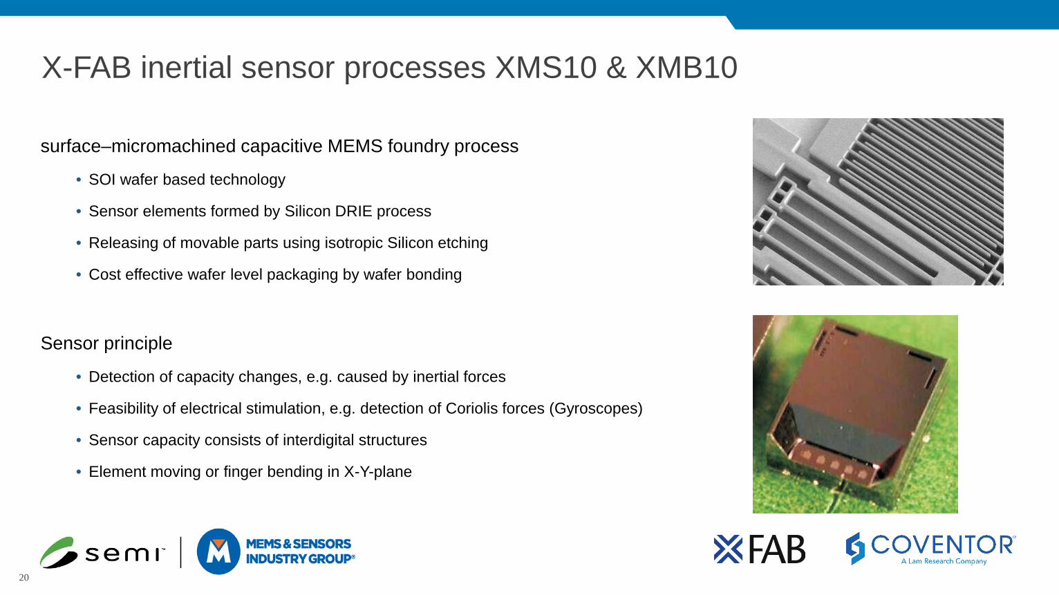
X-FAB inertial sensor processes XMS10 & XMB10
surface–micromachined capacitive MEMS foundry process
• SOI wafer based technology
• Sensor elements formed by Silicon DRIE process
• Releasing of movable parts using isotropic Silicon etching
• Cost effective wafer level packaging by wafer bonding
Sensor principle
• Detection of capacity changes, e.g. caused by inertial forces
• Feasibility of electrical stimulation, e.g. detection of Coriolis forces (Gyroscopes)
• Sensor capacity consists of interdigital structures
• Element moving or finger bending in X-Y-plane
20
X-FAB inertial sensor processes XMS10 & XMB10
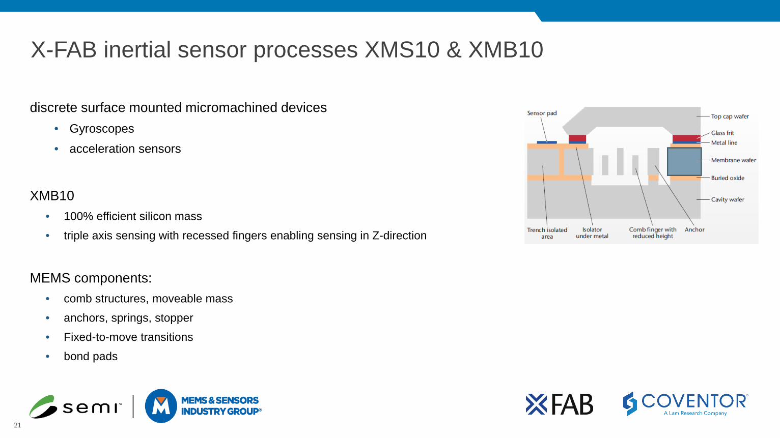
discrete surface mounted micromachined devices• Gyroscopes• acceleration sensors
XMB10• 100% efficient silicon mass• triple axis sensing with recessed fingers enabling sensing in Z-direction
MEMS components:• comb structures, moveable mass• anchors, springs, stopper• Fixed-to-move transitions• bond pads
21
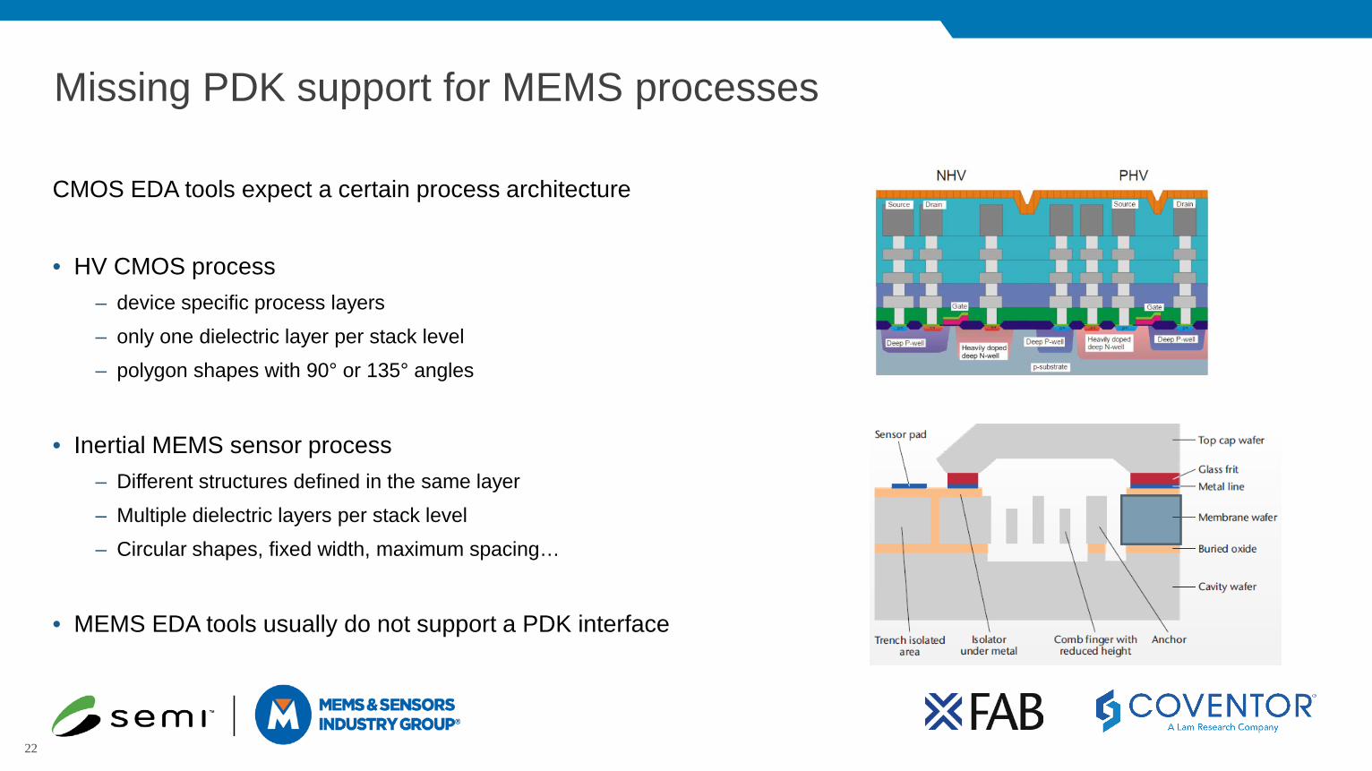
Missing PDK support for MEMS processes
CMOS EDA tools expect a certain process architecture
• HV CMOS process– device specific process layers– only one dielectric layer per stack level– polygon shapes with 90° or 135° angles
• Inertial MEMS sensor process– Different structures defined in the same layer– Multiple dielectric layers per stack level– Circular shapes, fixed width, maximum spacing…
• MEMS EDA tools usually do not support a PDK interface
22

Design flow: CMOS vs. MEMS
[https://www.youtube.com/watch?v=ZHhu0qSrurE]
• Digital CMOS• automated
• Analog HV CMOS
• Semi-automated
• MEMS• manual• Artwork: The quality
strongly depends on the artist…
23

• research project “Schematic-Based Design of MEMS for Applications in Optics and Robotics”, funding initial BMBF F&E 16M3093
• Project objective: “develop the first ever universal design methodology for MEMS to close the gap between electronics and mechanics design, manufacturing, and subsequent integration into products” [1]
• Project partners:
*
[1] MEMS2015: Schematic Driven MEMS Design for Applications in Optics and Robotics. (n.d.). Retrieved January 29, 2016, from https://www.edacentrum.de/en/projects/MEMS2015
* Coventor: Associated partner
24

• Similar to CMOS: MEMS PDK components enabling design flow
25
Coventor MEMS+ PDK and Design Flow
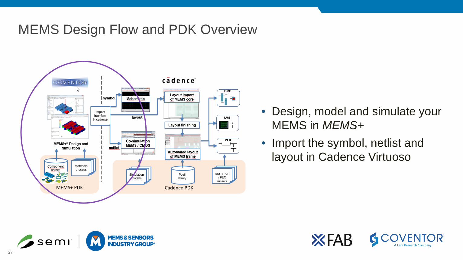
MEMS Design Flow and PDK Overview
• Design, model and simulate your MEMS in MEMS+
• Import the symbol, netlist and layout in Cadence Virtuoso
27

Coventor MEMS+® Library-Based Design: Enabling the Design FlowTechnology description• Material properties• Fabrication process
Visualize in 3DSimulate
MATLAB
Simulink
Virtuoso
Exported Verilog-A or Simulink ROM
MEMS+Simulator
Library of MEMS-specific,parametric components
Assemble Device
Export GDS2,Cadence PCells
28
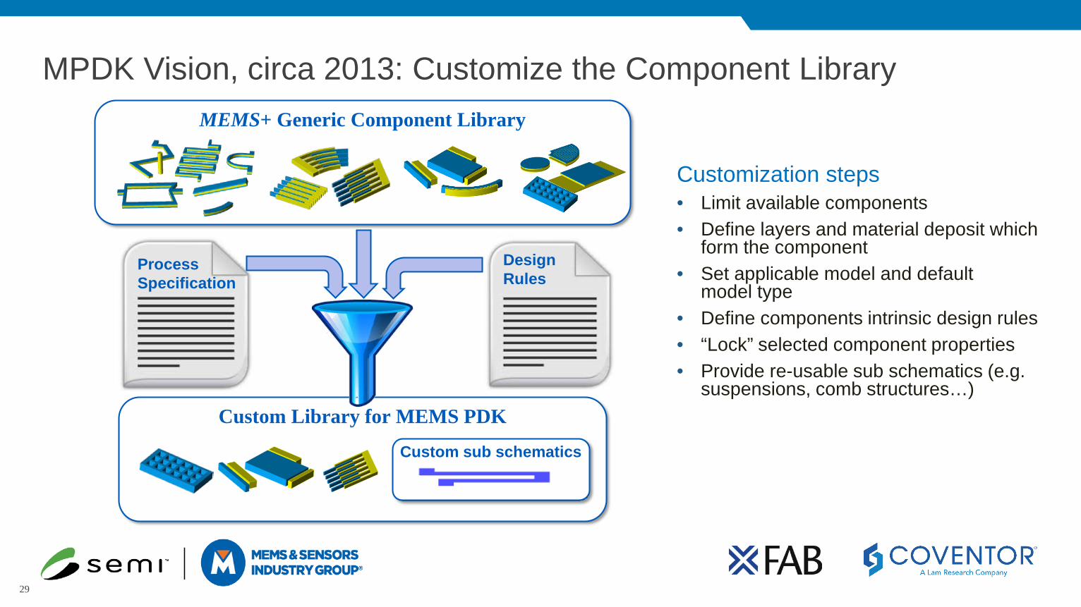
MPDK Vision, circa 2013: Customize the Component LibraryMEMS+ Generic Component Library
DesignRules
Custom Library for MEMS PDK
Custom sub schematics
ProcessSpecification
Customization steps• Limit available components• Define layers and material deposit which
form the component• Set applicable model and default
model type• Define components intrinsic design rules• “Lock” selected component properties• Provide re-usable sub schematics (e.g.
suspensions, comb structures…)
29

Design, Model and Simulation with XMB10 MEMS PDK
Coventor MEMS+ XMB10 Component Library
Single-Axis Accelerometer Core Assembled with MEMS+ XMB10 Library
Simulation in MEMS+ and Cadence VirtuosoY displacement and output capacitances as a results of the Y acceleration
Suspensions beams
Combs
Rigid, movable MASS
Anchor
Solid frame withMECH
Solid frame without MECH Metal1 Contact
30

Expanded Vision for Library-Based MEMS Design Enablement
Foundry MEMS PDK
Customer Device IP
MEMS+ Custom Component Library
Custom models
Suspension
Customer-Assembled Top-Level Design
MEMS device(s) Paths, PADs, frame
Custom Layout Add-OnsTSV
Path PAD
Foundry Device IPACC Z
ACC X,Y
GYRO Z
GYRO X,Y
Electrostatic element
31
Cadence Virtuoso PDK for X-FAB XMB10 Process

Cadence PDK and design flow overview
• Pcell-based layout finishing– Layer operations– Routing, connections to bond pads– Bonding frame generation for wafer-level packaging
• Verification– DRC, LVS, PEX
• Simulation with ADE
33

XMB10 SKILL pcell library
BondPad Bond pad with connection through the glass frit. Signal pads isolated by trench, ground pads not.
Crossing Bridges a wire through the MECH layer; isolated by trench
Comb Comb with variable finger count and pitch
FixedToMove Connection to moveable structures, crossing trench
Stopper Small MECH structure to limit the movement of the moveablemass in-plane
Frame All sensor surrounding structures required by process technology
34
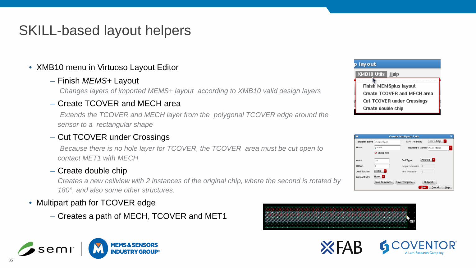
SKILL-based layout helpers
• XMB10 menu in Virtuoso Layout Editor– Finish MEMS+ Layout
Changes layers of imported MEMS+ layout according to XMB10 valid design layers
– Create TCOVER and MECH areaExtends the TCOVER and MECH layer from the polygonal TCOVER edge around the
sensor to a rectangular shape
– Cut TCOVER under CrossingsBecause there is no hole layer for TCOVER, the TCOVER area must be cut open to
contact MET1 with MECH
– Create double chipCreates a new cellview with 2 instances of the original chip, where the second is rotated by180°, and also some other structures.
• Multipart path for TCOVER edge– Creates a path of MECH, TCOVER and MET1
35
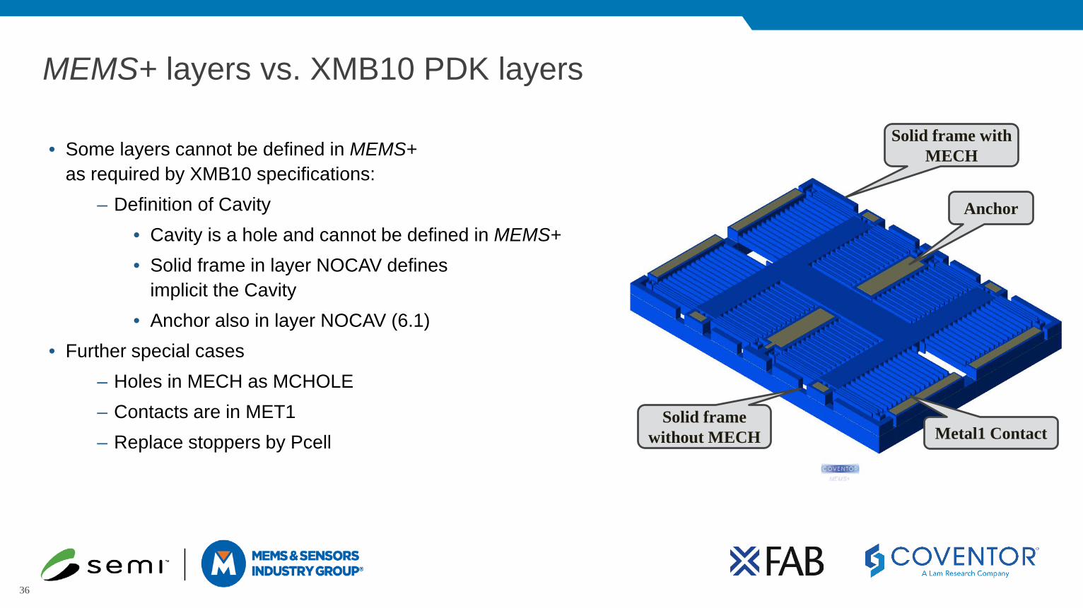
MEMS+ layers vs. XMB10 PDK layers
• Some layers cannot be defined in MEMS+as required by XMB10 specifications:
– Definition of Cavity• Cavity is a hole and cannot be defined in MEMS+• Solid frame in layer NOCAV defines
implicit the Cavity• Anchor also in layer NOCAV (6.1)
• Further special cases– Holes in MECH as MCHOLE– Contacts are in MET1– Replace stoppers by Pcell
Solid frame withMECH
Solid frame without MECH Metal1 Contact
Anchor
36
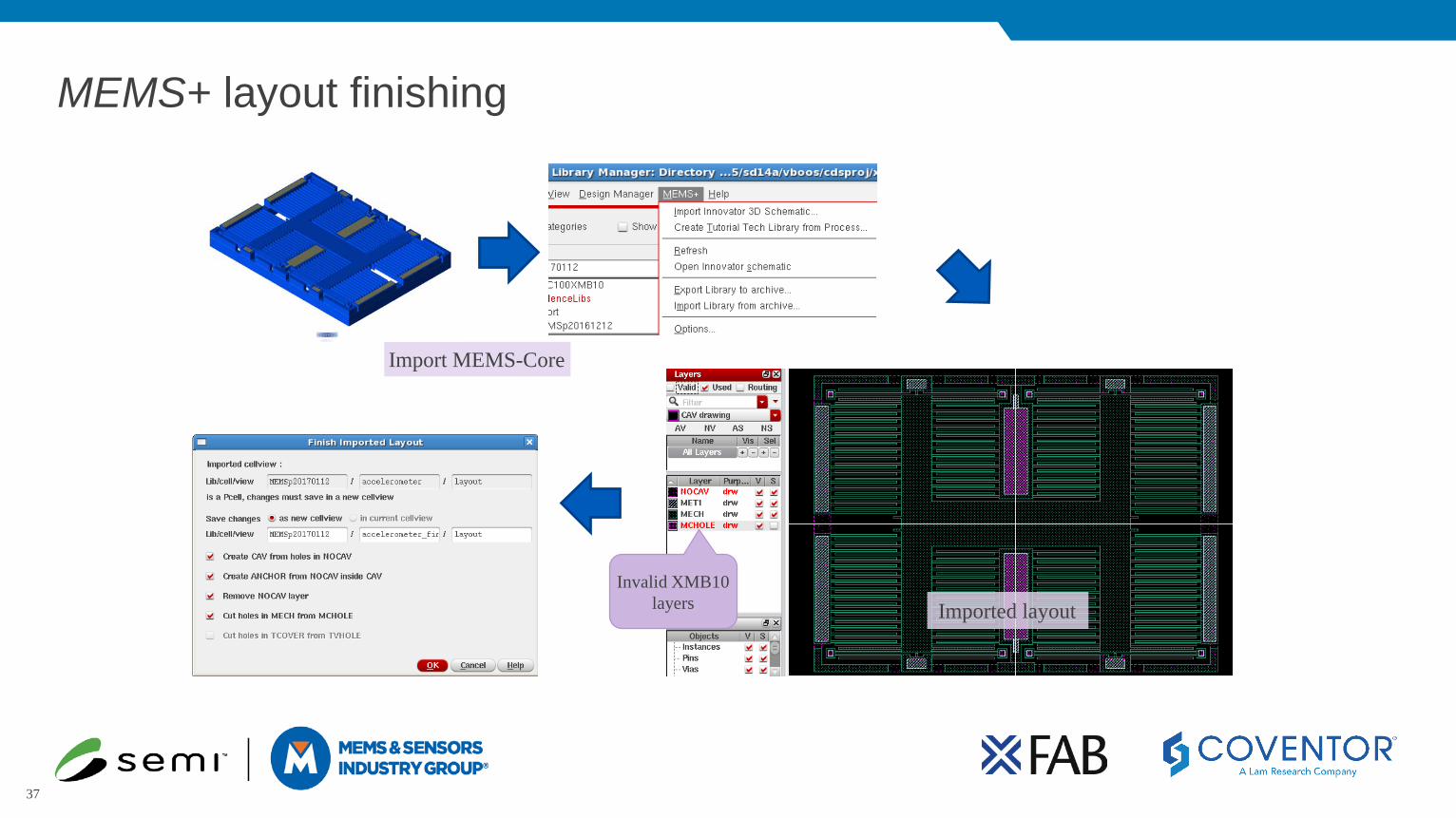
MEMS+ layout finishing
Import MEMS-Core
Imported layoutInvalid XMB10
layers
37

Routing area of the sensor
TCOVER forms a closed ring:
Fill TCOVER and MECH torectangular shape with script
Place „FixedToMove“ at sensor contacts
MECH/TCOVER Edgeas Multipart-Path
38

Routing and Bond Frame
Routing
Embedding sensor in Frame-Pcell
Crossing Pcell
39
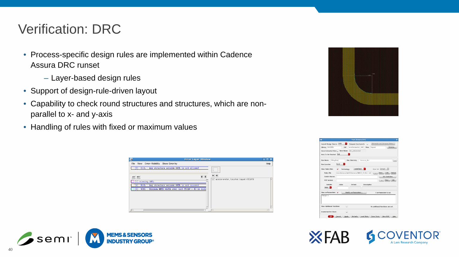
Verification: DRC
• Process-specific design rules are implemented within Cadence Assura DRC runset
– Layer-based design rules• Support of design-rule-driven layout• Capability to check round structures and structures, which are non-
parallel to x- and y-axis• Handling of rules with fixed or maximum values
40
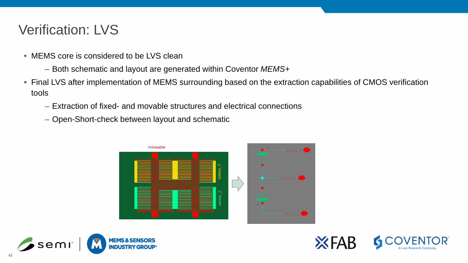
Verification: LVS
• MEMS core is considered to be LVS clean– Both schematic and layout are generated within Coventor MEMS+
• Final LVS after implementation of MEMS surrounding based on the extraction capabilities of CMOS verification tools
– Extraction of fixed- and movable structures and electrical connections– Open-Short-check between layout and schematic
41

Summary and Outlook
Summary• First foundry PDK for Coventor MEMS+ and Cadence Virtuoso available and ready to use
• Proven, ready-to-use Design Environment and Methodology using MEMS and CMOS design tools with a high level of design automation
– The parametric environment accelerates the optimization of sensor design parameters for a custom application
– The model generation enables system simulation and co-simulation with CMOS driver– The layout generation of the complete design is simplified thanks to automated flow.
Physical verification is supported
• The MEMS-PDK eases access to the technology for new customers and shortens time to market, by reducing design spins and fab cycles
– The PDK is the container for all technology information (process parameters, material characteristics, design layers, design rules …)
– Predefined process-specific components can be used to speed up the design
43

MEMS Design Contest
• MEMS design contest announced at DATE 2016
• Many design proposals have been submitted, based on X-FAB XMB10 process and CoventorMEMS+/Cadence Virtuoso PDK and design flow
• 10 semi-finalists have been selected by the sponsors
• Active design phase runs until end of 2017
• 3 winning designs will be presented at CDNLive EMEA 2018
• More information: http://info.coventor.com/mems-design-contest-2018
44
Thank you for your attention !Questions and Answers