Embed Size (px)
Citation preview
Hot electron effects in optically-pumped mid-infraredintersubband semiconductor laser
J W, J.-P. LBeckman Institute for Advanced Science and Technology and Center for Compound Semiconductor
Microelectronics, University of Illinois at Urbana-Champaign, Urbana, IL 61801, USA
F. H. JInstitut d’Electronique Fondamentale, URA 22 CNRS, Universite Paris XI, Bat 220, 91405 Orsay,
France
A. S’Division of Applied Physics, Hebrew University of Jerusalem, Jerusalem 91904, Israel
(Received 23 October 1995)
A theoretical investigation of an optically-pumped mid-infrared intersubband semiconductorlaser is presented. The influence of electrons and dopant ions on the conduction band struc-ture is simulated with a self-consistent Poisson–Schrodinger solver. Electron-polar opticalphonon interactions are calculated by using a macroscopic phonon model with electromag-netic boundary conditions. In order to assess the influence of the electronic temperature on thedevice optical performances, electron dynamics under optical pumping are investigated withina rate equation model where particle and energy flow equations are derived from Boltzmann’sequation with Fermi statistics. Our calculations show that population inversion between thefirst and second excited states can occur at 77 K under intersubband optical excitation.
( 1996 Academic Press Limited
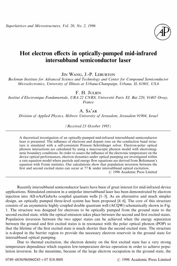
Recently intersubband semiconductor lasers have been of great interest for mid-infrared deviceapplications. Stimulated emission in a unipolar intersubband laser has been demonstrated by electroninjection into AlI-nAs/GaInAs coupled quantum wells [1–3]. As an alternative and much simplerdesign, an optically pumped three-level system has been proposed [4–6]. The core of this structureconsists of an asymmetric highly coupled double quantum well (ACQW) schematically shown in Fig.1. The structure was designed for electrons to be optically pumped from the ground state to thesecond excited state, while the optical emission takes place between the second and first excited states.Population inversion between the two upper states can be achieved when the energy separationbetween the ground and first excited states is in resonance with the polar optical phonon (POP) sothat the lifetime of the first excited state is much shorter than the second excited state. The structureis n-doped in the barrier region to provide the necessary electron reservoir in the ground state forintersubband optical pumping.
Due to thermal excitation, the electron density on the first excited state has a very strongtemperature dependence which requires low-temperature device operation in order to achieve popu-lation inversion. In the meantime, because of the large electron occupation in the ground state, the
SM ARTICLE 725 Revise 1st proof 1.2.96
Superlattices and Microstructures, Vol. 20, No. 2, 1996
0749–6036/96/060245]07 $18.00/0 ( 1996 Academic Press Limited
E3
36 meV
E2
E1
Em
issi
on
Opt
ical
pu
mpi
ng
Fig. 1. Schematic conduction band profile of the asymmetric coupled quantum well structure.
Pauli exclusion principle limits electron relaxation between the ground and first excited states at lowtemperature. Despite the fact that the stimulated gain increases with pumping intensity, the electrontemperature for each subband also increases which leads to a large thermal population in the firstexcited state and might reduce or even destroy the population inversion [4]. Therefore the develop-ment of theoretical models for the understanding of optical processes and carrier dynamics forperformance prediction has become technologically important. In this paper, we present a theoreticalinvestigation of the optically-pumped mid-infrared intersubband semiconductor laser at 77 K. Thetransition energies and electron Fermi level are determined by a self-consistent Poisson–Schrodingersolver [7] within the effective mass approximation. The transition probabilities for all types of elec-tron-POP interactions are calculated for confined (slab) and interface POP phonon modes [8]. Theelectron dynamics is studied by using a rate equation formalism [9] under optical pumping. Theelectron density, electron temperature, quasi-Fermi level, and average electron relaxation time con-stant for each subband are determined as a function of the pumping intensity.
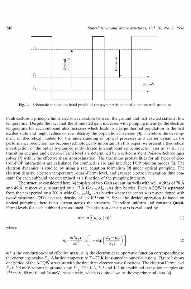
The structure considered here [4] consists of two GaAs quantum wells with well widths of 78 Aand 49 A, respectively, separated by a 17 A Ga
0.78Al
0.22As thin barrier. Each ACQW is separated
from the next period by a 200 A wide Ga0.78
Al0.22
As barrier where the center was n-type doped withtwo-dimensional (2D) electron density of 1]1011 cm~2. Since the device operation is based onoptical pumping, there is no current across the structure. Therefore uniform and constant Quasi-Fermi levels for each subband are assumed. The electron density n(z) is evaluated by
n(z)\; niDt
i(z) D2, (1)
where
ni\
m*kBT
nh~2lnC1]expA
Ef[E
zikBT BD , (2)
m* is the conduction-band effective mass, wi
is the electron envelope wave function corresponding tothe energy eigenvalue E
zi. A lattice temperature T\77 K is assumed in our calculations. Figure 2 shows
one period of the ACQW structure with the first three electron wave functions. The electron Fermi levelEf
is 2.5 meV below the ground state Ez1
. The 1–3, 2–3 and 1–2 intersubband transition energies are125 meV, 89 meV and 36 meV, respectively, which is quite close to the experimental data [4].
SM ARTICLE 725
Superlattices and Microstructures, Vol. 20, No. 2, 1996246
350
0.25
Length (A)
Con
duct
ion
ban
d po
ten
tial
(eV
)
250
0.2
0.15
0.1
0.05
50 100 150 200 3000
E3
E2
E1
Ef
Fig. 2. Self-consistent conduction band potential, electron quasi-Fermi level and the first three electron wavefunctions in the ACQW structure for n\1011 cm~2.
To simulate electron dynamics in the ACQW structure, we use a rate equation approach whichis derived from Boltzmann’s equation with Fermi statistics [9] and is less computer-intensive than theMonte-Carlo method. One major drawback of this approach is that the shape of the electron dis-tribution function remains Fermi-like, whereas the Monte-Carlo method provides a distributionprofile dictated by electron dynamics. However, this is not a problem in our case because the pump-ing power is high enough for electrons to thermalize immediately in each subband. Here the Fermidistribution f
*(k
i) of subband i with quantized energy E
zi, electron temperature T
iand quasi-Fermi
level Efi
is
fi(k
i)\
1e*EAi(kAi)`Ezi~Efi+@kTi]1
,
where EEiis the electron kinetic energy for ith subband in the parallel direction. The use of the Fermi
distribution implicitly assumes that electron–electron intrasubband scattering is strong enough tocreate a Fermi distribution within each subband. We have assumed intersubband electron–electronscattering to be negligible since it requires large momentum exchange and large electron density [10].The general procedure for the calculation of the electron dynamics with this approach is to firstassume an initial condition in the ACQW structure in thermal equilibrium, i.e. without optical pump-ing. The electron temperature is assumed to be the lattice temperature T\77 K, the quasi-Fermi levelof each subband is reduced to E
fi\E
fand the electron population n
ion each subband is given by
eqn (2). The average transverse energy SEiT is evaluated by
SEiT\
m*(kTi)2
ninh~2 P
=
0
xdxexp[x[(E
fi[E
zi)/kT
i]]1
(3)
SM ARTICLE 725
Superlattices and Microstructures, Vol. 20, No. 2, 1996 247
1012
Pumping power (kW cm2)
Ele
ctro
n d
ensi
ty (
cm2 )
108
107
106
105
10–2 10–1 104
109
1010
1011
100 101 102 103
n1
n2
n3
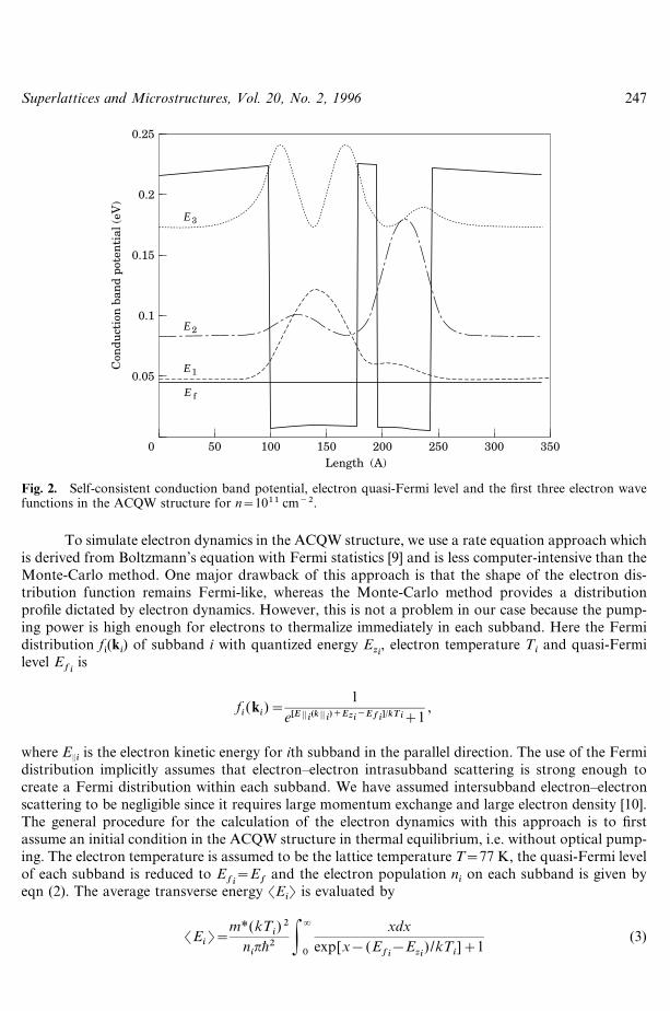
Fig. 3. Electron density ni
in each subband i as a function of optical pumping intensity under the steady statefor n\1011 cm~2.
where the integral is defined as the Fermi integral of order one. By using the initial values of Efi
andTi, the first and second moment equations are evaluated and the values of n
iand SE
iT are updated
after each time step. Then the electron temperature Ti
and the quasi-Fermi level Efi
are updated bysolving eqns (2) and (3) self-consistently, and the calculation is repeated for a new time step untilsteady state is reached for a given optical pumping power.
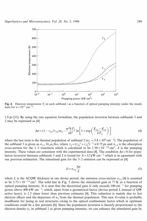
In Fig. 3, we show the electron density n3
on subband 3 increasing exponentially withpumping intensity until about 1]1010 cm~2 and then gradually saturating. At the same timethe electron density n
2on subband 2 remains constant for low pumping intensity up to 10 kW
cm~2 and then gradually increases as photoexcited electrons cascade down from subband 3.The population inversion between subbands M2, 3N occurs for a pumping intensity of 12 kWcm~2 and above. Since the electron density n
3on subband 3 increases much faster than the
electron density n2
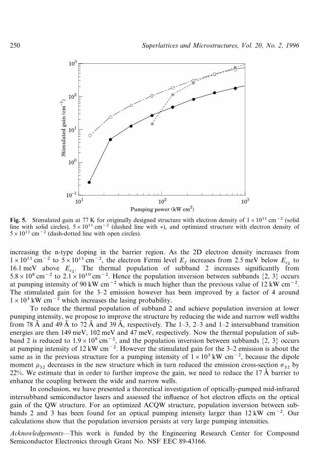
on subband 2, the population inversion will not be destroyed at high pumpingintensity. In fact, population inversion increases monotonically as the pumping intensity increasesup to 103 kW cm~2. As shown in Fig. 4, the electron temperature increases very quickly athigh pumping intensity because the electron system in the ACQW structure is rapidly gainingenergy from optical pumping before phonon dissipations cool down the system. In particular,the electron temperature T
2on subband 2 is increasing much faster than T
1and T
3. However,
the population increase in n2
is partially due to heating effects in subband 1, which thermallyexcite electrons into subband 2. It is readily seen on Fig. 4 that n
2starts to increase when
T1
deviates from 77 K at 10D20 kW cm~2. In the meantime, because of the population inversionbetween subbands 2 and 3, more highly energetic electrons also transfer from subband 3 intosubband 2 which also contributes to the n
2-deviation from thermal occupation. Our calculations
show that the effective relaxation time constants s21
, s31
, and s32
are not very sensitive to theoptical pumping intensity. The effective relaxation time s
21from subband 2 to subband 1 is
about 0.27 ps, while the effective relaxation time s32
from subband 3 to subband 2 is about
SM ARTICLE 725
Superlattices and Microstructures, Vol. 20, No. 2, 1996248
Pumping power (kW cm2)
Ele
ctro
n t
empe
ratu
re (
K)
010–2 10–1 104
600
100 101 102 103
T1
700
500
400
300
200
100
T2
T3
Fig. 4. Electron temperature Ti
in each subband i as a function of optical pumping intensity under the steadystate for n\1011 cm~2.
1.8 ps [11]. By using the rate equation formalism, the population inversion between subbands 3 and2 may be expressed as [4]
*n\(1[q21
/q23
)n3[
m*kT2
nh~2lnC1]expA
Ef2
[Ez2
kT2
BD (4)
where the last term is the thermal population of subband 2 (n2
\5.8]108 cm~2). The population ofthe subband 3 is given as r
13Ss
3n1/h~x, where s
3\(s~1
31]s~1
32)~1B0.75 ps and r
13is the absorption
cross-section for the 1–3 transition which is calculated to be 1.50]10~14 cm2, S is the pumpingintensity. These values are consistent with the experimental data [4]. The condition Dn\0 for popu-lation inversion between subbands 3 and 2 is found for S\12 kW cm~2 which is in agreement withour previous estimation. The stimulated gain for the 3–2 emission can be expressed as [4]
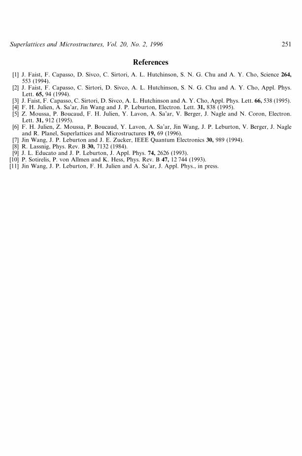
G\p32
*nL
(5)
where L is the ACQW thickness in one device period, the emission cross-section r32
[4] is assumedto be 3.75]10~14 cm2. The solid line in Fig. 5 shows the stimulated gain at 77 K as a function ofoptical pumping intensity. It is seen that the theoretical gain G only exceeds 100 cm~1 for pumpingpower above 400 kW cm~2, which, apart from a geometrical factor (device period L instead of QWactive layer), is 1.5 times lower than previous estimates [4]. This reduction is mainly due to hotelectron effects and the departure of n
2from the thermal population. This new G-value is probably
insufficient for lasing in real structures owing to the optical confinement factor which in optimumconditions could be a few percents [6]. Since the population inversion is linearly proportional to theelectron density n
1in subband 1 at given pumping intensity, we can enhance the stimulated gain by
SM ARTICLE 725
Superlattices and Microstructures, Vol. 20, No. 2, 1996 249
103
Pumping power (kW cm2)
Sti
mu
late
d ga
in (
cm–1
)*
**
*
*
102
101
100
10–1
101 102 103
Fig. 5. Stimulated gain at 77 K for originally designed structure with electron density of 1]1011 cm~2 (solidline with solid circles), 5]1011 cm~2 (dashed line with \), and optimized structure with electron density of5]1011 cm~2 (dash-dotted line with open circles).
increasing the n-type doping in the barrier region. As the 2D electron density increases from1]1011 cm~2 to 5]1011 cm~2, the electron Fermi level E
fincreases from 2.5 meV below E
z1to
16.1 meV above Ez1
. The thermal population of subband 2 increases significantly from5.8]108 cm~2 to 2.1]1010 cm~2. Hence the population inversion between subbands M2, 3N occursat pumping intensity of 90 kW cm~2 which is much higher than the previous value of 12 kW cm~2.The stimulated gain for the 3–2 emission however has been improved by a factor of 4 around1]103 kW cm~2 which increases the lasing probability.
To reduce the thermal population of subband 2 and achieve population inversion at lowerpumping intensity, we propose to improve the structure by reducing the wide and narrow well widthsfrom 78 A and 49 A to 72 A and 39 A, respectively. The 1–3, 2–3 and 1–2 intersubband transitionenergies are then 149 meV, 102 meV and 47 meV, respectively. Now the thermal population of sub-band 2 is reduced to 1.9]109 cm~2, and the population inversion between subbands M2, 3N occursat pumping intensity of 12 kW cm~2. However the stimulated gain for the 3–2 emission is about thesame as in the previous structure for a pumping intensity of 1]103 kW cm~2, because the dipolemoment l
32decreases in the new structure which in turn reduced the emission cross-section r
32by
22%. We estimate that in order to further improve the gain, we need to reduce the 17 A barrier toenhance the coupling between the wide and narrow wells.
In conclusion, we have presented a theoretical investigation of optically-pumped mid-infraredintersubband semiconductor lasers and assessed the influence of hot electron effects on the opticalgain of the QW structure. For an optimized ACQW structure, population inversion between sub-bands 2 and 3 has been found for an optical pumping intensity larger than 12 kW cm~2. Ourcalculations show that the population inversion persists at very large pumping intensities.
Acknowledgements—This work is funded by the Engineering Research Center for CompoundSemiconductor Electronics through Grant No. NSF EEC 89-43166.
SM ARTICLE 725
Superlattices and Microstructures, Vol. 20, No. 2, 1996250
References
[1] J. Faist, F. Capasso, D. Sivco, C. Sirtori, A. L. Hutchinson, S. N. G. Chu and A. Y. Cho, Science 264,553 (1994).
[2] J. Faist, F. Capasso, C. Sirtori, D. Sivco, A. L. Hutchinson, S. N. G. Chu and A. Y. Cho, Appl. Phys.Lett. 65, 94 (1994).
[3] J. Faist, F. Capasso, C. Sirtori, D. Sivco, A. L. Hutchinson and A. Y. Cho, Appl. Phys. Lett. 66, 538 (1995).[4] F. H. Julien, A. Sa’ar, Jin Wang and J. P. Leburton, Electron. Lett. 31, 838 (1995).[5] Z. Moussa, P. Boucaud, F. H. Julien, Y. Lavon, A. Sa’ar, V. Berger, J. Nagle and N. Coron, Electron.
Lett. 31, 912 (1995).[6] F. H. Julien, Z. Moussa, P. Boucaud, Y. Lavon, A. Sa’ar, Jin Wang, J. P. Leburton, V. Berger, J. Nagle
and R. Planel, Superlattices and Microstructures 19, 69 (1996).[7] Jin Wang, J. P. Leburton and J. E. Zucker, IEEE Quantum Electronics 30, 989 (1994).[8] R. Lassnig, Phys. Rev. B 30, 7132 (1984).[9] J. L. Educato and J. P. Leburton, J. Appl. Phys. 74, 2626 (1993).
[10] P. Sotirelis, P. von Allmen and K. Hess, Phys. Rev. B 47, 12 744 (1993).[11] Jin Wang, J. P. Leburton, F. H. Julien and A. Sa’ar, J. Appl. Phys., in press.
SM ARTICLE 725
Superlattices and Microstructures, Vol. 20, No. 2, 1996 251


![Graphene modelocked VECSELs · Ultrafast vertical-external-cavity surface -emitting lasers (VECSELs )[4], also known as semiconductor disk lasers (SDLs) [5] or optically pumped semiconductor](https://img.pdfslide.us/doc/110x75/5f09805b7e708231d4272096/graphene-modelocked-vecsels-ultrafast-vertical-external-cavity-surface-emitting.jpg)