Embed Size (px)
Citation preview
Hopping conduction distance dependent activation energy characteristics of Zn:SiO2resistance random access memory devicesKai-Huang Chen, Rui Zhang, Ting-Chang Chang, Tsung-Ming Tsai, Kuan-Chang Chang, J. C. Lou, Tai-Fa
Young, Jung-Hui Chen, Chih-Cheng Shih, Cheng-Wei Tung, Yong-En Syu, and Simon M. Sze Citation: Applied Physics Letters 102, 133503 (2013); doi: 10.1063/1.4799655 View online: http://dx.doi.org/10.1063/1.4799655 View Table of Contents: http://scitation.aip.org/content/aip/journal/apl/102/13?ver=pdfcov Published by the AIP Publishing
This article is copyrighted as indicated in the article. Reuse of AIP content is subject to the terms at: http://scitation.aip.org/termsconditions. Downloaded to IP:
185.41.20.103 On: Mon, 17 Mar 2014 13:47:05
Hopping conduction distance dependent activation energy characteristicsof Zn:SiO2 resistance random access memory devices
Kai-Huang Chen,1,a) Rui Zhang,2 Ting-Chang Chang,3,4,a) Tsung-Ming Tsai,5
Kuan-Chang Chang,5 J. C. Lou,2 Tai-Fa Young,6 Jung-Hui Chen,7 Chih-Cheng Shih,7
Cheng-Wei Tung,5 Yong-En Syu,3 and Simon M. Sze8
1Department of Electronics Engineering and Computer Science, Tung-Fang Design University,Kaohsiung, Taiwan2School of Software and Microelectronics, Peking University, Beijing 100871, People’s Republic of China3Department of Physics, National Sun Yat-Sen University, Kaohsiung 804, Taiwan4Advanced Optoelectronics Technology Center, National Cheng Kung University, Tainan 700, Taiwan5Department of Materials and Optoelectronic Science, National Sun Yat-Sen University, Kaohsiung,804, Taiwan6Department of Mechanical and Electro-Mechanical Engineering, National Sun Yat-Sen University,Kaohsiung, Taiwan7Department of Chemistry, National Kaohsiung Normal University, Kaohsiung, Taiwan8Department of Electronics Engineering, National Chiao Tung University, Hsinchu 300, Taiwan
(Received 20 February 2013; accepted 21 March 2013; published online 2 April 2013)
In this study, the hopping conduction distance variation of Zn:SiO2 resistance random access
memory (RRAM) devices with different operating compliance currents was discussed and
verified. To investigate and determine the hopping conduction distance dependent activation
energy characteristics, the Arrhenius plot of low resistance state of Zn:SiO2 RRAM devices was
applied, from which we proposed carrier conduction model. With the increase of current
compliance, more metal ions would accumulate to form precipitates with larger diameter, which
in turn resulted in the shortening of hopping distance. Because of shorter hopping distance,
activation energy for carrier hopping would decrease. VC 2013 American Institute of Physics.
[http://dx.doi.org/10.1063/1.4799655]
Recently, the non-volatile random access memory devi-
ces were widely discussed and investigated for applications,
including resistance random access memory (RRAM), ferro-
electric random access memory (FeRAM), magnetic random
access memory (MRAM), and phase change memory
(PCM).1–9 Among these memory devices, silicon oxide based
RRAM devices attract vast attention owing to great compati-
bility in integrated circuit (IC) processes, non-destructive
readout, low operation voltage, high operation speed, long
retention time, and simple structure.10–15
Various materials have been reported having resistance
switching properties.16–24 And zinc is an extensively
researched material in semiconductor device.25–29 In this let-
ter, the resistive switching mechanism of zinc-doped SiO2
RRAM was thoroughly analyzed. In the experiment, we
found that the low resistance state (LRS) of Zn:SiO2 RRAM
devices using different operating compliance currents had
different hopping distances. Besides, the hopping conduction
distance dependent activation energy was investigated by the
Arrhenius plot, which also confirmed the hopping distance
variation.
Metal-insulator-metal (MIM) structure for RRAM devi-
ces, which was fabricated over a polished p-Si wafer with
nominal resistance �1.0 X cm, was schematically shown in
inset of Fig. 1. Native-oxide, contaminant particles, and
metal ions on silicon wafer were removed during RCATM
clean process. In order to remove contaminants of metal
target and obtain relative pure plasma during deposition
time, pre-sputtering was maintained for 30 min under argon
ambient. The Zn:SiO2 thin film was later deposited on the
TiN/Ti/SiO2/Si substrate by co-sputtering with pure SiO2
and zinc targets. The sputtering power was fixed with RF
power 200 W and DC power 10 W for silicon dioxide and
zinc targets, respectively. Additionally, the Pt top electrode
with a thickness of 200 nm was deposited on Zn:SiO2 film to
form Pt/Zn:SiO2/TiN sandwich structure by DC magnetron
sputtering. The entire electrical measurements of devices
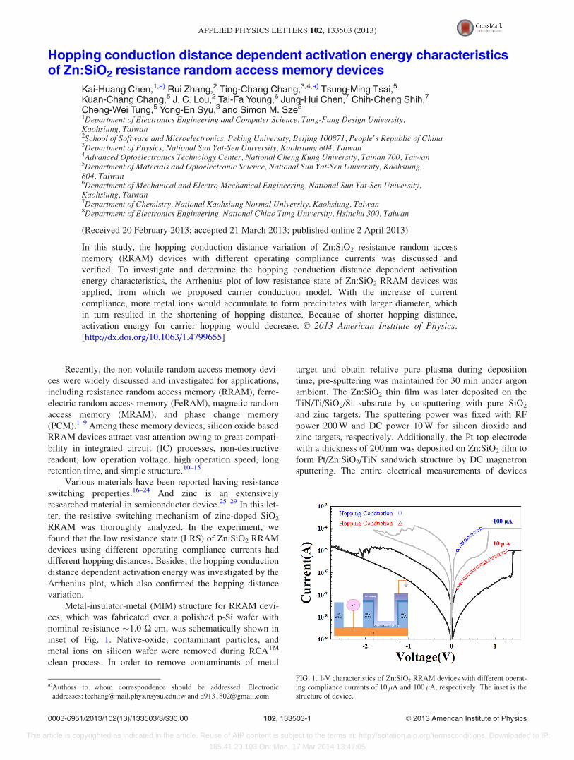
FIG. 1. I-V characteristics of Zn:SiO2 RRAM devices with different operat-
ing compliance currents of 10 lA and 100 lA, respectively. The inset is the
structure of device.
a)Authors to whom correspondence should be addressed. Electronic
addresses: [email protected] and [email protected]
0003-6951/2013/102(13)/133503/3/$30.00 VC 2013 American Institute of Physics102, 133503-1
APPLIED PHYSICS LETTERS 102, 133503 (2013)
This article is copyrighted as indicated in the article. Reuse of AIP content is subject to the terms at: http://scitation.aip.org/termsconditions. Downloaded to IP:
185.41.20.103 On: Mon, 17 Mar 2014 13:47:05
with the Pt electrode of 4 lm diameter were performed using
Agilent B1500 semiconductor parameter analyzer.
Figure 1 shows the typical I-V curves of Zn:SiO2
RRAM devices under different operating compliance cur-
rents of 10 lA and 100 lA, respectively. By conduction
current fitting, both LRS with different operating compliance
currents were dominated by hopping conduction mechanism.
From comparison, we could find that the I-V window with
higher current compliance was escalated by nearly two order
magnitude.
To investigate the resistance switching behaviors in
Zn:SiO2 RRAM with different compliance currents, the rela-
tionship between LRS and temperature was measured as
shown in Figs. 2(a) and 2(b). We could observe in both
Figures 2(a) and 2(b) that current increased with the rising
temperature, which was similar to semiconductor current-
temperature property. According to the equation of hopping
conduction, J ¼ qNat0e�q/T=kTeqaV=2dkT , where N, a, /T , t0,
and d are density of space charge, mean of hopping distance,
barrier height of hopping, intrinsic vibration frequency,
and film thickness, respectively, we can draw out the curve
/T-aV/2d with a vertical axis of In(I) and a lateral axis of
1/kT (Figure 2(c) for 10 lA of compliance current, Fig. 2(d)
for 100 lA). From Figs. 2(c) and 2(d), we could observe that
experimental data matched with hooping conduction equa-
tion, which was also testified by our previous current fitting
(Figure 1).
In order to further investigate the characteristics of hop-
ping conduction with different current compliances, activa-
tion energy verses voltage were drew out in Figure 3.
Arrhenius equation was applied to analyze the relationship
between activation energy and voltage. The activation
energy equation is EA;exp ¼ � @ logI@ð 1
kTÞ, where Ea is active
energy, k is the Boltzmann’s constant, and T is the absolute
temperature. The intercept of vertical axis represent their
corresponding activation energy. And from Figure 3, we
could obtain the activation energy of 10 lA and 100 lA com-
pliance current operating situation, which were 0.1533 eV
and 0.0682 eV, respectively. With the increase of current
compliance, activation energy dropped from 0.1533 eV to
0.0682 eV.
Furthermore, hopping distance could be extracted from
Arrhenius equation. As EA;exp ¼ � @ logI
@ 1 1kTð Þ¼ EC � EF �qVA
Dz2ua
,
FIG. 2. (a) and (b) are the current tempera-
ture relationship for 10 lA and 100 lA cur-
rent compliance, respectively. (c) and (d)
are their corresponding hopping equation
plots.
FIG. 3. The activation energy and volt-
age properties for 10 lA and 100 lA
compliance current operating situation.
133503-2 Chen et al. Appl. Phys. Lett. 102, 133503 (2013)
This article is copyrighted as indicated in the article. Reuse of AIP content is subject to the terms at: http://scitation.aip.org/termsconditions. Downloaded to IP:
185.41.20.103 On: Mon, 17 Mar 2014 13:47:05
we could get dEA
dVA¼ qDzð2uaÞ, where EA is activation energy, VA is
applied voltage, Dz is average hopping distance, and ua is the
thickness of switching layer. According to our previous
research,24 the thickness of switching layer is about 5 nm,
namely ua equals to 5 nm. What’s more dEA
dVAcan be obtained
from Figure 3, it is the slope of fitting curve. By substituting dEA
dVA
and ua into dEA
dVA¼ qDzð2uaÞ, hopping distance can be obtained,
which are 1.44 nm for 10 lA compliance operating situation
0.3 nm for 100 lA compliance operating situation,
respectively.
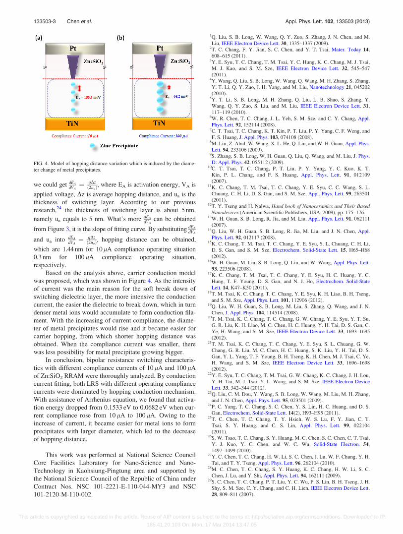
Based on the analysis above, carrier conduction model
was proposed, which was shown in Figure 4. As the intensity
of current was the main reason for the soft break down of
switching dielectric layer, the more intensive the conduction
current, the easier the dielectric to break down, which in turn
denser metal ions would accumulate to form conduction fila-
ment. With the increasing of current compliance, the diame-
ter of metal precipitates would rise and it became easier for
carrier hopping, from which shorter hopping distance was
obtained. When the compliance current was smaller, there
was less possibility for metal precipitate growing bigger.
In conclusion, bipolar resistance switching characteris-
tics with different compliance currents of 10 lA and 100 lA
of Zn:SiO2 RRAM were thoroughly analyzed. By conduction
current fitting, both LRS with different operating compliance
currents were dominated by hopping conduction mechanism.
With assistance of Arrhenius equation, we found that activa-
tion energy dropped from 0.1533 eV to 0.0682 eV when cur-
rent compliance rose from 10 lA to 100 lA. Owing to the
increase of current, it became easier for metal ions to form
precipitates with larger diameter, which led to the decrease
of hopping distance.
This work was performed at National Science Council
Core Facilities Laboratory for Nano-Science and Nano-
Technology in Kaohsiung-Pingtung area and supported by
the National Science Council of the Republic of China under
Contract Nos. NSC 101-2221-E-110-044-MY3 and NSC
101-2120-M-110-002.
1Q. Liu, S. B. Long, W. Wang, Q. Y. Zuo, S. Zhang, J. N. Chen, and M.
Liu, IEEE Electron Device Lett. 30, 1335–1337 (2009).2T. C. Chang, F. Y. Jian, S. C. Chen, and Y. T. Tsai, Mater. Today 14,
608–615 (2011).3Y. E. Syu, T. C. Chang, T. M. Tsai, Y. C. Hung, K. C. Chang, M. J. Tsai,
M. J. Kao, and S. M. Sze, IEEE Electron Device Lett. 32, 545–547
(2011).4Y. Wang, Q. Liu, S. B. Long, W. Wang, Q. Wang, M. H. Zhang, S. Zhang,
Y. T. Li, Q. Y. Zuo, J. H. Yang, and M. Liu, Nanotechnology 21, 045202
(2010).5Y. T. Li, S. B. Long, M. H. Zhang, Q. Liu, L. B. Shao, S. Zhang, Y.
Wang, Q. Y. Zuo, S. Liu, and M. Liu, IEEE Electron Device Lett. 31,
117–119 (2010).6W. R. Chen, T. C. Chang, J. L. Yeh, S. M. Sze, and C. Y. Chang, Appl.
Phys. Lett. 92, 152114 (2008).7C. T. Tsai, T. C. Chang, K. T. Kin, P. T. Liu, P. Y. Yang, C. F. Weng, and
F. S. Huang, J. Appl. Phys. 103, 074108 (2008).8M. Liu, Z. Abid, W. Wang, X. L. He, Q. Liu, and W. H. Guan, Appl. Phys.
Lett. 94, 233106 (2009).9S. Zhang, S. B. Long, W. H. Guan, Q. Liu, Q. Wang, and M. Liu, J. Phys.
D: Appl. Phys. 42, 055112 (2009).10C. T. Tsai, T. C. Chang, P. T. Liu, P. Y. Yang, Y. C. Kuo, K. T.
Kin, P. L. Chang, and F. S. Huang, Appl. Phys. Lett. 91, 012109
(2007).11K. C. Chang, T. M. Tsai, T. C. Chang, Y. E. Syu, C. C. Wang, S. L.
Chuang, C. H. Li, D. S. Gan, and S. M. Sze, Appl. Phys. Lett. 99, 263501
(2011).12T. Y. Tseng and H. Nalwa, Hand book of Nanoceramics and Their Based
Nanodevices (American Scientific Publishers, USA, 2009), pp. 175–176.13W. H. Guan, S. B. Long, R. Jia, and M. Liu, Appl. Phys. Lett. 91, 062111
(2007).14Q. Liu, W. H. Guan, S. B. Long, R. Jia, M. Liu, and J. N. Chen, Appl.
Phys. Lett. 92, 012117 (2008).15K. C. Chang, T. M. Tsai, T. C. Chang, Y. E. Syu, S. L. Chuang, C. H. Li,
D. S. Gan, and S. M. Sze, Electrochem. Solid-State Lett. 15, H65–H68
(2012).16W. H. Guan, M. Liu, S. B. Long, Q. Liu, and W. Wang, Appl. Phys. Lett.
93, 223506 (2008).17K. C. Chang, T. M. Tsai, T. C. Chang, Y. E. Syu, H. C. Huang, Y. C.
Hung, T. F. Young, D. S. Gan, and N. J. Ho, Electrochem. Solid-State
Lett. 14, K47–K50 (2011).18T. M. Tsai, K. C. Chang, T. C. Chang, Y. E. Syu, K. H. Liao, B. H. Tseng,
and S. M. Sze, Appl. Phys. Lett. 101, 112906 (2012).19Q. Liu, W. H. Guan, S. B. Long, M. Liu, S. Zhang, Q. Wang, and J. N.
Chen, J. Appl. Phys. 104, 114514 (2008).20T. M. Tsai, K. C. Chang, T. C. Chang, G. W. Chang, Y. E. Syu, Y. T. Su,
G. R. Liu, K. H. Liao, M. C. Chen, H. C. Huang, Y. H. Tai, D. S. Gan, C.
Ye, H. Wang, and S. M. Sze, IEEE Electron Device Lett. 33, 1693–1695
(2012).21T. M. Tsai, K. C. Chang, T. C. Chang, Y. E. Syu, S. L. Chuang, G. W.
Chang, G. R. Liu, M. C. Chen, H. C. Huang, S. K. Liu, Y. H. Tai, D. S.
Gan, Y. L. Yang, T. F. Young, B. H. Tseng, K. H. Chen, M. J. Tsai, C. Ye,
H. Wang, and S. M. Sze, IEEE Electron Device Lett. 33, 1696–1698
(2012).22Y. E. Syu, T. C. Chang, T. M. Tsai, G. W. Chang, K. C. Chang, J. H. Lou,
Y. H. Tai, M. J. Tsai, Y. L. Wang, and S. M. Sze, IEEE Electron Device
Lett. 33, 342–344 (2012).23Q. Liu, C. M. Dou, Y. Wang, S. B. Long, W. Wang, M. Liu, M. H. Zhang,
and J. N. Chen, Appl. Phys. Lett. 95, 023501 (2009).24P. C. Yang, T. C. Chang, S. C. Chen, Y. S. Lin, H. C. Huang, and D. S.
Gan, Electrochem. Solid-State Lett. 14(2), H93–H95 (2011).25T. C. Chen, T. C. Chang, T. Y. Hsieh, W. S. Lu, F. Y. Jian, C. T.
Tsai, S. Y. Huang, and C. S. Lin, Appl. Phys. Lett. 99, 022104
(2011).26S. W. Tsao, T. C. Chang, S. Y. Huang, M. C. Chen, S. C. Chen, C. T. Tsai,
Y. J. Kuo, Y. C. Chen, and W. C. Wu, Solid-State Electron. 54,
1497–1499 (2010).27Y. C. Chen, T. C. Chang, H. W. Li, S. C. Chen, J. Lu, W. F. Chung, Y. H.
Tai, and T. Y. Tseng, Appl. Phys. Lett. 96, 262104 (2010).28M. C. Chen, T. C. Chang, S. Y. Huang, K. C. Chang, H. W. Li, S. C.
Chen, J. Lu, and Y. Shi, Appl. Phys. Lett. 94, 162111 (2009).29S. C. Chen, T. C. Chang, P. T. Liu, Y. C. Wu, P. S. Lin, B. H. Tseng, J. H.
Shy, S. M. Sze, C. Y. Chang, and C. H. Lien, IEEE Electron Device Lett.
28, 809–811 (2007).
FIG. 4. Model of hopping distance variation which is induced by the diame-
ter change of metal precipitates.
133503-3 Chen et al. Appl. Phys. Lett. 102, 133503 (2013)
This article is copyrighted as indicated in the article. Reuse of AIP content is subject to the terms at: http://scitation.aip.org/termsconditions. Downloaded to IP:
185.41.20.103 On: Mon, 17 Mar 2014 13:47:05