Embed Size (px)
Citation preview

This work is licensed under a Creative Commons Attribution 3.0 License. For more information, see http://creativecommons.org/licenses/by/3.0/.
This article has been accepted for publication in a future issue of this journal, but has not been fully edited. Content may change prior to final publication. Citation information: DOI 10.1109/TPEL.2017.2773459, IEEETransactions on Power Electronics
TPEL-Reg-2017-04-0579 1
Abstract— A highly efficient 5-kW bidirectional DC-DC
converter power stage operating from a 400-V supply implementing Super-Junction (SJ) MOSFETs is presented. SJ MOSFETs have low on-state resistances and low switching losses. However, their application in voltage-source converters can be compromised by the reverse recovery behavior of their intrinsic diodes and their highly non-linear output capacitances. A series switching-aid circuit is used to control the output capacitance charging current. The dead times between switching transitions are assessed and optimized in order to deactivate the intrinsic diodes. The combination of these techniques enables very high efficiencies to be attained. Calorimetric measurements indicate a full-load efficiency of 99.1% for the prototype 5-kW DC-DC converter power stage. A loss reduction of approximately 50% is achieved with the prototype converter power stage when compared to an equivalent IGBT based power stage. Lastly, a loss vs. duty cycle function is experimentally determined which can be used to inform the design of a maximum efficiency point tracking system.
Index Terms— Dead time control, intrinsic diode deactivation, metal-oxide-semiconductor field-effect transistor (MOSFET), output capacitance, super-junction.
I. INTRODUCTION
OSFETS are renowned for their fast switching speeds, current sharing capability when paralleled, and the ease
with which their gates can be driven [1]. Their application at high voltages is limited due to the exponential increase in on-state resistance 𝑅 ( ) with blocking voltage for a given device area. Super-junction (SJ) MOSFETs [2][3] use columns of n and p-type doping in the device’s drift region, to lower the 𝑅 ( ) for a given blocking voltage. These devices are available with blocking voltage capabilities of 500-950 V, e.g. [4]. There are, however, two inherent problems which hinder
Manuscript received April 4, 2017; accepted October 28, 2017. This work was supported by the UK Engineering and Physical Sciences Research Council (www.epsrc.ac.uk, Grant No. EP/I038543/1, Vehicle Electical Systems Integration (VESI)).
A. N. Hopkins, P. Proynov, B. Stark and P. H. Mellor are with the Department of Electrical and Electronic Engineering, University of Bristol,
their adoption in voltage source converters (VSCs). The first is that when the MOSFET is off, reverse conduction causes a high concentration of minority carriers to be injected into the device, thus increasing the charge that needs to be extracted in order for the device to block voltage in the forward direction. This poor reverse recovery behavior of its intrinsic body diode causes additional switching loss [5]. The second is the large and highly non-linear output capacitance 𝐶 [2] which, when coupled with the device’s fast switching performance, leads to high 𝑑𝑉/𝑑𝑡 and 𝑑𝑖/𝑑𝑡 transients. These transients cause excessive stress to the switching devices and could cause premature device failure [6]. At higher voltages the power dissipation incurred due to supplying the charge drawn by 𝐶 is one of the most significant loss mechanisms in VSCs. For this reason, IGBTs with lower output capacitances and without intrinsic diodes that would pass high reverse recovery charge are traditionally favored in VSCs beyond 200 V.
In mains-voltage applications, where converter efficiency and power density are the critical design criteria, wide bandgap (WBG) semiconductor devices and SJ MOSFETs are being investigated as alternatives to the IGBT [7]. On the one hand, WBG devices draw a negligible reverse recovery current and have a lower 𝐶 for the same current rating [8]. These devices still cost significantly more than SJ MOSFETs, and other problems need to be addressed, such as the low gate voltage margin of GaN FETs, or the life degradation of gate oxides in SiC MOSFETs [9]. Established SJ devices remain attractive alternatives to IGBTs and wide-bandgap devices, provided their poor switching behavior at higher voltages can be addressed. The intrinsic diode can be deactivated [10]-[12] to reduce reverse recovery loss, or the devices themselves need to be modified to improve reverse recovery [13].
To ensure that the intrinsic diode remains inactive in a VSC phase-leg, the reverse-conducting SJ MOSFET is, ideally, kept
Bristol, UK (e-mail: [email protected], [email protected], [email protected], [email protected])
N. McNeill is with the Department of Electronic and Electrical Engineering, University of Strathclyde, Glasgow, UK (e-mail: [email protected]).
Achieving Efficiencies Exceeding 99% in a Super-Junction 5-kW DC-DC Converter Power Stage
Through the Use of an Energy Recovery Snubber and Dead Time Optimization
Andrew Hopkins, Member, IEEE, Plamen Proynov, Neville McNeill, Bernard Stark and Phil Mellor, Member, IEEE
M

This work is licensed under a Creative Commons Attribution 3.0 License. For more information, see http://creativecommons.org/licenses/by/3.0/.
This article has been accepted for publication in a future issue of this journal, but has not been fully edited. Content may change prior to final publication. Citation information: DOI 10.1109/TPEL.2017.2773459, IEEETransactions on Power Electronics
TPEL-Reg-2017-04-0579 2
on until its current drops to zero, when the complementary device is turned on. Once turned off, the device can therefore return to its blocking state, without the presence of minority carriers. This requires care to avoid shoot-through where both MOSFETs conduct, and a precise coordination of the activation of the high and low-side drivers would be needed. Predictive and adaptive gate driving has been reported for automotive applications at voltages in the 30V-40V range using 55-V [14] and 75-V [15] devices, where an optimal gate signal overlap is found which minimizes the sum of reverse recovery loss and shoot-through loss. In this manner the point of maximum conversion efficiency can be found. Whilst MEPT can minimize diode recovery charge, it cannot eliminate the charge which must be supplied into a devices’ 𝐶 . Therefore, at higher voltages, no such maximum efficiency point tracking (MEPT) schemes have been reported. Split-inductor techniques are reported in [16] and [17] to address the intrinsic diode recovery in 400-V super junction circuits, at the expense of adding magnetic component volume. Using the split-inductor technique, a DC-AC or AC-DC converter is essentially formed by combining two single-ended converters such that each converter manages the input or output current during alternate AC base frequency half-cycles. In this way the power devices have to act either as high-frequency forward switches or high-frequency rectifiers, but not both. However, challenges are that four-quadrant operation requires more complexity, magnetic component (choke) utilization is poor, and that current waveform distortion is incurred when the changeover between half-cycles occurs.
This paper presents a theoretical analysis, and experimental verification of a method for maximizing power stage conversion efficiency by dead time optimization for a 5-kW DC/DC bidirectional converter for automotive applications, using 600-V SJ MOSFETs. The circuit uses an inductive switching-aid circuit [18] with energy-recovery to facilitate the optimal dead time estimation, avoid destructive 𝑑𝑉/𝑑𝑡 and 𝑑𝑖/𝑑𝑡 transients, and significantly reduce 𝐶 charging loss. This results in a converter power stage (excluding the input and output filter components and gate drivers) with 99.1% full-load efficiency, as measured by calorimetry.
II. MAXIMIZING SWITCHING EFFICIENCY USING AN ENERGY-RECOVERY INDUCTIVE SNUBBER
A. Energy-Recovery Snubber
The inductive snubber [18] used here is a switching-aid circuit that transfers energy incurred by sourcing the intrinsic diode recovery and 𝐶 charges drawn by the freewheeling SJ MOSFET into a recovery circuit that returns the energy to the DC-rail. The principle is shown in Fig. 1: the inductance 𝐿 , of the coupled inductor primary winding, is located in the path of the diode reverse recovery 𝑄 and output capacitance 𝑄 charge-flow. A switched-mode power supply (SMPS) connected to a secondary winding can be used to return the energy stored in the snubber inductor back into the supply rail [19].
Fig. 1. Energy recovery inductive snubber configuration.
The circuit operates as follows: Starting with the control device S1 off, the synchronous device (SR) S2 on and reverse conducting, the current 𝐼 is free-wheeling in the direction indicated in Fig. 1. On initiation of the S1 turn-on switching action, S2 is left on as long as possible to avoid current transfer into the body-diode in S2 and thus to minimize the build-up of minority carriers. Upon turn-on of S1, the energy needed for any reverse recovery of the body diode and to charge the output capacitance of S2 is transferred from the DC link to S2 via the primary winding of the inductor. The presence of the inductor lowers and broadens the current surge, minimizing the losses associated with the charge transfer. At the end of the switching transient the stored energy in the inductance is transferred via the secondary winding 𝑁 to the input of the SMPS and returned into the DC link. To avoid reverse recovery of the S2 intrinsic diode, the turn-off of the S2 MOSFET needs to be precisely controlled. Inclusion of the snubber inductance is beneficial as it slows down the commutation process and thus reduces the demands on the accuracy of this timing. Furthermore, the reset power transferred via 𝑁 provides a measure of switching-associated loss (i.e. the loss associated with managing the flow of charge into the power device acting as the rectifier) and the onset of shoot-through on a cycle-by-cycle basis, thus providing a signal that can be used to optimize the relative timings of the gate signals for MEPT.
The added inductance also acts to reduce the switching voltage transient 𝑑𝑉/𝑑𝑡 and the consequent ringing and voltage stresses. Referring to Fig. 2, a SJ MOSFET can be modelled as an ideal transistor with an anti-parallel diode, and a non-linear output capacitance 𝐶 (𝑉 ) that is a strong function of device voltage 𝑉 . Therefore the charge against voltage function 𝑄 (𝑉 ) is also highly nonlinear, Fig. 2b. The area above the QV curve in Fig. 2b represents the MOSFET’s self-discharge energy which largely determines switching loss in single-ended applications. On the other hand, the area under the curve represents the associated co-energy. This is much larger and determines the power that would be dissipated in the incoming switch in a hard-switched VSC bridge-leg in the course of charging Coss.
NsN
Ls
S1
S2
SMPS
ISR
Vout
VRAIL

This work is licensed under a Creative Commons Attribution 3.0 License. For more information, see http://creativecommons.org/licenses/by/3.0/.
This article has been accepted for publication in a future issue of this journal, but has not been fully edited. Content may change prior to final publication. Citation information: DOI 10.1109/TPEL.2017.2773459, IEEETransactions on Power Electronics
TPEL-Reg-2017-04-0579 3
a) Equivalent capacitance model b) Charge versus voltage relationship
Fig. 2. TK62J60W [4] SJ MOSFET’s output characteristics.
During the switching transient the sharp knee in the 𝑄 (𝑉 ) characteristic causes the voltage across S2 to rise rapidly after the bulk of 𝑄 has been supplied, causing unwanted voltage stresses in the circuit. The introduction of inductance in the path via which 𝑄 is supplied suppresses this by limiting the peak current flowing into 𝐶 . With this peak current thus limited, the 𝑑𝑉/𝑑𝑡 in the low-capacitance region above the knee-point is consequently reduced.
B. Effect of Gate Signal Underlap/Overlap on Energy Recovery
The point at which the S2 MOSFET channel turns-off has a significant effect on the peak current sourced into it at commutation. The peak commutation current, 𝐼 , determines the stresses placed upon the control MOSFET and the power 𝑊 that is transferred into the snubber inductor:
In (1) 𝑉 is the supply voltage, 𝑄 is the aggregate of any intrinsic diode reverse recovery 𝑄 and 𝑄 charge within S2, and 𝑓 is the switching frequency. A rectangular approximation can be assumed due to the high non-linearity of the output capacitance [18]. As S2 is commutated off, the body diode reverse recovery charge is supplied first and 𝑄 is then supplied as the switch voltage VDS rises
Fig. 3 illustrates the commutation current waveforms
resulting from different timings of gating the S2 MOSFET off. In Fig. 3a the MOSFET is inactive during the switching transient and as a result the intrinsic diode conducts the full load current. The full reverse recovery charge must be supplied along with that required to charge the output capacitance 𝑄 . Fig. 3b shows the case where a small overlap occurs in the SR MOSFET switching. The charge transferred to the intrinsic diode is now reduced, and the consequent total reverse recovery charge is decreased, leading to a reduction in the peak commutation current, 𝐼 .
The variation in diode reverse recovery charge with forward current is typically approximated as a linear relationship:
𝑄 = 𝑘 𝐼 (2)
where the gradient 𝑘 can be found from a linear interpolation of the 𝑄 versus 𝐼 characteristic in the device datasheet. However, in the case of a MOSFET, the reverse recovery charge measurement, 𝑄 , supplied in the datasheets is effectively the combined values of 𝑄 and 𝑄 [18]; thus:
𝑄 = 𝑄 + 𝑘 ( )𝐼 (3)
where 𝑘 ( ) is a modified coefficient to account for the presence of 𝑄 . Neglecting the small on-state device voltage drop in the devices, the rate of change of current is determined by the inductance of 𝐿 and the supply voltage:
𝑑𝐼
𝑑𝑡= −𝑉 /𝐿 (4)
Now 𝐼 is given by:
𝐼 =
𝑉 𝑡
𝐿 (5)
Putting the result from (5) into (3) gives:
𝑄 = 𝑄 +
𝑉 𝑡
𝐿𝑘 ( ) (6)
If S2 is turned off after 𝐼 has started to fall, 𝑄 is passed during the interval (𝑡 ) from 𝐼 = 0 to 𝐼 = -𝐼 such that:
a) No overlap, S2 gated off with or before S1, full load current transferred into diode.
b) Insufficient overlap, S2 gated off early allowing partial load current transfer into diode.
c) Optimal overlap timing S2 gated off at zero current. d) S2 gated off late.
Fig. 3. Illustrative 𝐼 waveform zooms of the S1-on/S2-off switching transition for four different switching scenarios (a-d). [18]
𝑊 = 𝑉 𝑄 𝑓 (1)
Qrr
IPK
Qoss
0A
ISR
S1 on, S2 off
S2 off
Qrr
IPK
Qoss
0A
ISR
S1 on
IPK
0A
QossS2 off
ISR
S1 on
S2 off
Qoss
IPK
0A
ISR
S1 on
t0

This work is licensed under a Creative Commons Attribution 3.0 License. For more information, see http://creativecommons.org/licenses/by/3.0/.
This article has been accepted for publication in a future issue of this journal, but has not been fully edited. Content may change prior to final publication. Citation information: DOI 10.1109/TPEL.2017.2773459, IEEETransactions on Power Electronics
TPEL-Reg-2017-04-0579 4
𝑄 =
𝐼 𝑡
2 (7)
𝑡 is given by:
𝑡 =
𝐿 𝐼
𝑉 (8)
Putting the result from (8) into (7) yields:
𝑄 =
𝐿 𝐼
2𝑉 (9)
Equating (6) and (9), and solving for 𝐼 yields:
𝐼 =
2𝑉 𝑄
𝐿+
2𝑉 𝑡 𝑘 ( )
𝐿 (10)
The peak commutation current will be a minimum and the circuit operation is at its most efficient operating point when there is no reverse recovery charge associated with the diode. Fig. 3c illustrates this optimum point (at 𝐼 = 0 A). Only the 𝑄 of the device must be supplied as the intrinsic diode is deactivated.
Should S2 turn off beyond the optimal point, Fig. 3d, an excess negative current will be built up, before the 𝑄 charge is transferred. In this case the resultant increased peak commutation current is:
𝐼 =
2𝑉 𝑄
𝐿+
𝑉 𝑡
𝐿 , (11)
where to is the overrun beyond the optimal overlap time.
C. Predicted Reset Energy
Fig. 4 shows the optimum switching scenario, where 𝐼 is at its minimum. The optimum gate switching of S2 should result in overlap time determined from:
𝑡 _ =
𝐿 𝐼
𝑉 (12)
Deviations from the optimal timing will result in additional loss due to the increase in 𝐼 . The total energy transfer into the snubber inductance over a switching cycle will be the combination of the commutation energy of S2 and the energy transferred through 𝐿 in establishing the load current within S2 at turn-off of S1. At steady state the power transfer into the snubber inductance can be calculated using (13), with 𝐼 found using either (10) or (11).
𝑊 = 𝑓𝐿
𝐼 + 𝐼
2 (13)
Fig. 4. Minimum energy switching showing the optimum overlap time.
III. POWER CIRCUITRY AND PREDICTED RESULTS
A schematic of the experimental converter power stage is shown in Fig. 5 and a photograph of the prototype is shown in Fig. 6. The circuitry operates without forced cooling. Component details are listed in Table I. The design was for an input voltage range between 200-400 V and a continuous output up to 22 A and 5 kW. The output current was controlled by a variable duty pulse width modulation with integrated dead time adjustment. The switching frequency was set to 25 kHz.
The device selection was optimized in order to choose a suitable SJ MOSFET, trading off between conduction (𝑅 ( )) and switching (𝐶 ) loss characteristics using the figure of merit outlined in [20]. A range of devices from different manufacturers and numbers of devices in parallel were analyzed to determine the optimum combination which will achieve the least losses for an appropriate price. The selected SJ MOSFET, Toshiba TK62J60W, has an 𝑅 ( ) of 33 mΩ and three devices were connected in parallel to form each switch, S1-3 and S4-6 respectively in Fig 5. These six power devices are shown mounted on the heatsink in Fig. 6. 18.2-Ω and 8.2-Ω series gate resistors were used for the control and SR devices respectively in order to achieve suitable switching rise and fall times.
The device output capacitance charge versus voltage characteristics (QV curves) were found from the manufacturers’ supplied capacitance data [21]. A 𝑄 of 1.4 μC is expected at 400-V operation for the three devices in parallel forming each switch. Furthermore, the device datasheet shows a total reverse charge of 7 μC at a current of 31 A in the intrinsic diode. Accounting for the inclusion of 𝑄 in the charge measurement, the reverse recovery coefficient, 𝑘 ( ), given in (3) is estimated as 210 ns.
Fig. 5. A schematic diagram of the experimental converter power stage,
showing snubber and overvoltage clamps. Component values are given in Table I.
IPK
0A
QossS2 off
ISR
S1 on
topt_overlap

This work is licensed under a Creative Commons Attribution 3.0 License. For more information, see http://creativecommons.org/licenses/by/3.0/.
This article has been accepted for publication in a future issue of this journal, but has not been fully edited. Content may change prior to final publication. Citation information: DOI 10.1109/TPEL.2017.2773459, IEEETransactions on Power Electronics
TPEL-Reg-2017-04-0579 5
Fig. 6. Photograph of experimental circuitry. No forced cooling is applied.
TABLE I. CIRCUIT COMPONENT DATA.
S1-6 Toshiba TK62J60W MOSFET
L1
1.38 μH; Micrometals T130-6 core; Main winding -12 turns of 100 strands of Litz enamelled 0.2-mm dia. Cu wire; Reset
winding - 12 turns of a single stranded enamelled 1-mm dia. Cu wire.
R1 Four 10-Ω resistors in series R2/R3 Two 1-kΩ 2-W resistors connected in parallel R4/R5 1 Ω, 2 W resistors
C1 4.7 nF DEBB33A472KA3B C2 1.5 μF R82DC4150Z260J C3 4.7 nF DEBB33A472KA3B
C4/C6 220 pF C5 100 pF, 6 kV C7 Three 3.3 µF BTC233820335 in parallel D1 C4D05120E D2 SCS220AMC D3 C3D04060A
The snubber inductor 𝐿 and reset circuitry are shown in Fig. 6 situated in front of the MOSFETs. 𝐿 was constructed from a Micrometals T130-6 toroidal core [22]. The main and reset windings had each 12 turns, giving a measured inductance of 1.38 μH. The peak AC flux density excursion in the inductor core was calculated to be 45 mT. Multi-stranded Litz wire was used for the main winding to mitigate skin-effect losses and the reset winding was interleaved with the main winding to minimize leakage inductances [23]. For simplicity and ease of measurement the energy recovered through the reset winding was initially dissipated in a fixed resistor, 𝑅1. A four-wire measurement of this resistance gave 41.6 Ω. 𝑅1 is remotely mounted onto a separate heatsink in order to isolate any thermal effect of the dump losses on the main switching devices. The power dissipated in 𝑅1 was later returned to the supply via an SMPS as described in [19]. Fig. 7 shows an outline diagram and a photograph of the simple flyback SMPS that was implemented to achieve recovery of the switching-associated losses. The circuit operates under input voltage control to maintain Vreset constant. A high efficiency SMPS has also been reported in [24], operating at similar input and output voltages.
An overvoltage appears across the off-going power switches when the stored energy in the snubber inductor is reset. Assuming ideal coupling of the inductor reset winding, this overvoltage 𝑉 is given by:
𝑉 =
𝑁
𝑁𝑉 , (14)
where 𝑉 is the operating voltage of the reset circuit. In
Fig. 7. Top: Outline diagram of simple flyback SMPS used for energy
recovery. Bottom: Photograph of the demonstrator energy recovery SMPS.
practice the coupling will not be perfect, manifesting as a series leakage inductance. Additional circuitry formed with R2, R3, C2, C3, D2, and D3 was included in the test circuit to dissipate the leakage energy and clamp the consequent over-voltages. Further components R4, C6, R5, C4 and C5 were included to suppress high frequency oscillations observed at the drain of the parallel connected MOSFETs S4-S6, and acted to improve the quality of the presented measured waveform traces as well as lowering any associated EMI.
The test circuit initially used a resistor, 𝑅 , on the secondary of 𝐿 to dissipate the reset energy. The transferred power can be determined from a measurement of the RMS voltage, 𝑉 , across the resistor by:
𝑉 = 𝑊 𝑅 (15)
IV. EXPERIMENTAL RESULTS
A. Experimental Set-Up
The tests are performed using the experimental set-up shown in Fig. 8. The test procedure is automated in order to facilitate fast and accurate measurement of important circuit parameters. Initially the input voltage and the duty ratio for the PWM gate driving signals are set manually. A MATLAB script controls a signal generator to sweep the timing of the S2 gate circuit from -220 ns to 80 ns. Over the sweep oscilloscope waveforms of the following parameters are collected: input voltage, snubber inductance current, timing reference voltage and output current. The data is acquired by the oscilloscope at a sufficiently high sampling frequency and streamed to the MATLAB PC via USB. After the acquisition the waveform data is used to calculate the peak snubber inductor current and the RMS reset voltage Vreset.
Vreset
PWMcontroller-
+
Vreset
(set point)
VRAIL
Vreset
(error)
Σ
D1
T1
TR1
Vreset(rtn)
This work is licensed under a Creative Commons Attribution 3.0 License. For more information, see http://creativecommons.org/licenses/by/3.0/.
This article has been accepted for publication in a future issue of this journal, but has not been fully edited. Content may change prior to final publication. Citation information: DOI 10.1109/TPEL.2017.2773459, IEEETransactions on Power Electronics
TPEL-Reg-2017-04-0579 6
Fig. 8. Experimental set-up.
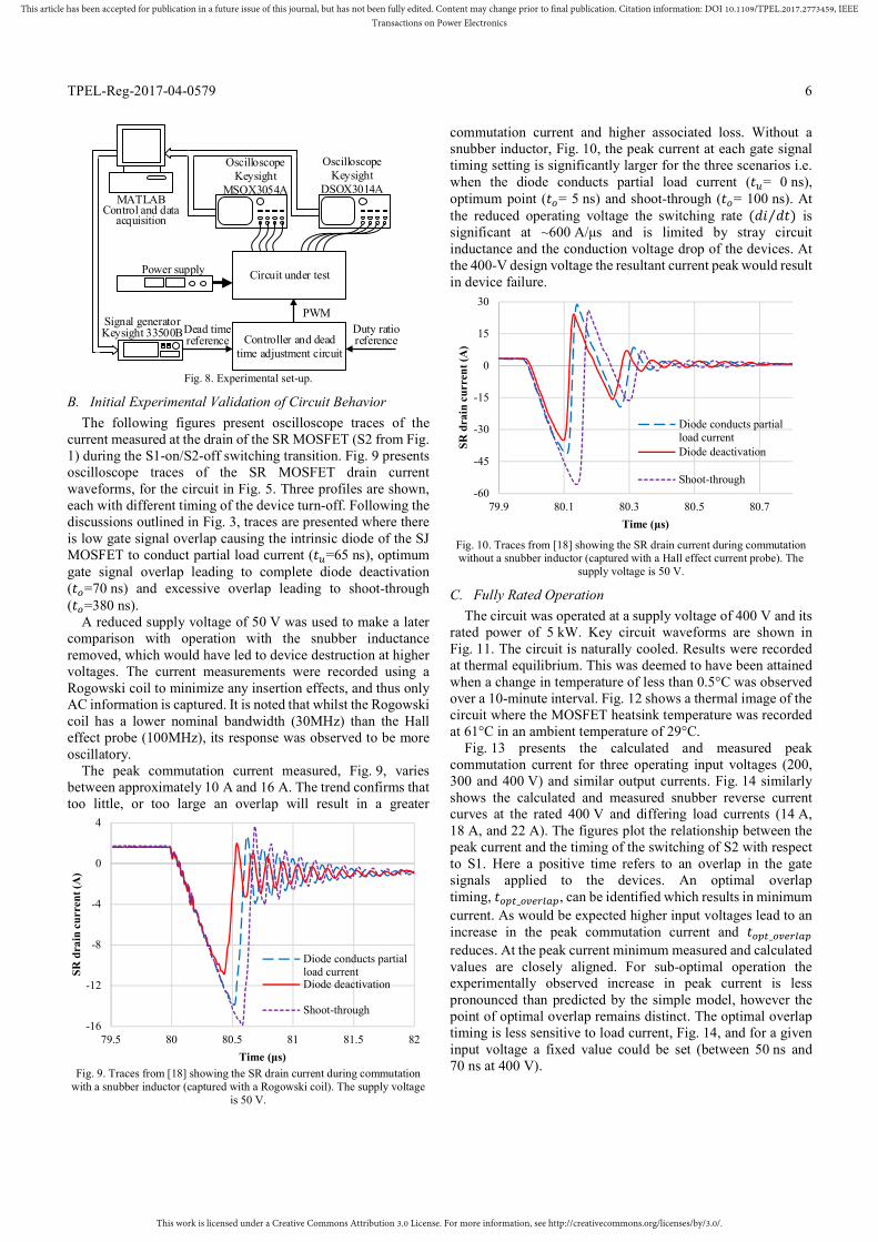
B. Initial Experimental Validation of Circuit Behavior
The following figures present oscilloscope traces of the current measured at the drain of the SR MOSFET (S2 from Fig. 1) during the S1-on/S2-off switching transition. Fig. 9 presents oscilloscope traces of the SR MOSFET drain current waveforms, for the circuit in Fig. 5. Three profiles are shown, each with different timing of the device turn-off. Following the discussions outlined in Fig. 3, traces are presented where there is low gate signal overlap causing the intrinsic diode of the SJ MOSFET to conduct partial load current (𝑡 =65 ns), optimum gate signal overlap leading to complete diode deactivation (𝑡 =70 ns) and excessive overlap leading to shoot-through (𝑡 =380 ns).
A reduced supply voltage of 50 V was used to make a later comparison with operation with the snubber inductance removed, which would have led to device destruction at higher voltages. The current measurements were recorded using a Rogowski coil to minimize any insertion effects, and thus only AC information is captured. It is noted that whilst the Rogowski coil has a lower nominal bandwidth (30MHz) than the Hall effect probe (100MHz), its response was observed to be more oscillatory.
The peak commutation current measured, Fig. 9, varies between approximately 10 A and 16 A. The trend confirms that too little, or too large an overlap will result in a greater
Fig. 9. Traces from [18] showing the SR drain current during commutation
with a snubber inductor (captured with a Rogowski coil). The supply voltage is 50 V.
commutation current and higher associated loss. Without a snubber inductor, Fig. 10, the peak current at each gate signal timing setting is significantly larger for the three scenarios i.e. when the diode conducts partial load current (𝑡 = 0 ns), optimum point (𝑡 = 5 ns) and shoot-through (𝑡 = 100 ns). At the reduced operating voltage the switching rate (𝑑𝑖 𝑑𝑡⁄ ) is significant at ~600 A/μs and is limited by stray circuit inductance and the conduction voltage drop of the devices. At the 400-V design voltage the resultant current peak would result in device failure.
Fig. 10. Traces from [18] showing the SR drain current during commutation without a snubber inductor (captured with a Hall effect current probe). The
supply voltage is 50 V.
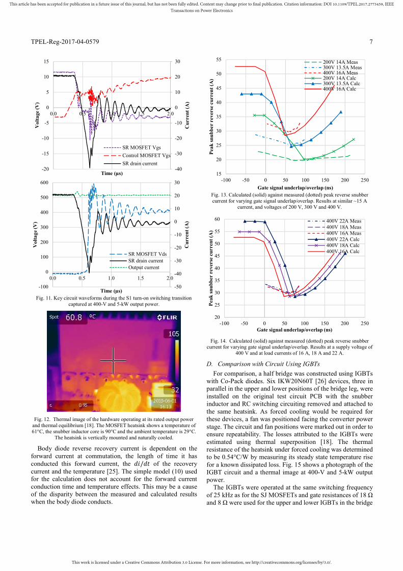
C. Fully Rated Operation
The circuit was operated at a supply voltage of 400 V and its rated power of 5 kW. Key circuit waveforms are shown in Fig. 11. The circuit is naturally cooled. Results were recorded at thermal equilibrium. This was deemed to have been attained when a change in temperature of less than 0.5°C was observed over a 10-minute interval. Fig. 12 shows a thermal image of the circuit where the MOSFET heatsink temperature was recorded at 61°C in an ambient temperature of 29°C.
Fig. 13 presents the calculated and measured peak commutation current for three operating input voltages (200, 300 and 400 V) and similar output currents. Fig. 14 similarly shows the calculated and measured snubber reverse current curves at the rated 400 V and differing load currents (14 A, 18 A, and 22 A). The figures plot the relationship between the peak current and the timing of the switching of S2 with respect to S1. Here a positive time refers to an overlap in the gate signals applied to the devices. An optimal overlap timing, 𝑡 _ , can be identified which results in minimum current. As would be expected higher input voltages lead to an increase in the peak commutation current and 𝑡 _ reduces. At the peak current minimum measured and calculated values are closely aligned. For sub-optimal operation the experimentally observed increase in peak current is less pronounced than predicted by the simple model, however the point of optimal overlap remains distinct. The optimal overlap timing is less sensitive to load current, Fig. 14, and for a given input voltage a fixed value could be set (between 50 ns and 70 ns at 400 V).
Oscilloscope Keysight
MSOX3054AMATLAB
Control and data acquisition
Oscilloscope Keysight
DSOX3014A
Circuit under testPower supply
Controller and dead time adjustment circuit
Dead time reference
PWMSignal generatorKeysight 33500B Duty ratio
reference
-16
-12
-8
-4
0
4
79.5 80 80.5 81 81.5 82
SR d
rain
cur
rent
(A
)
Time (μs)
Diode conducts partialload currentDiode deactivation
Shoot-through
-60
-45
-30
-15
0
15
30
79.9 80.1 80.3 80.5 80.7
SR d
rain
cur
ren
t (A
)
Time (μs)
Diode conducts partialload currentDiode deactivation
Shoot-through
This work is licensed under a Creative Commons Attribution 3.0 License. For more information, see http://creativecommons.org/licenses/by/3.0/.
This article has been accepted for publication in a future issue of this journal, but has not been fully edited. Content may change prior to final publication. Citation information: DOI 10.1109/TPEL.2017.2773459, IEEETransactions on Power Electronics
TPEL-Reg-2017-04-0579 7
Fig. 11. Key circuit waveforms during the S1 turn-on switching transition
captured at 400-V and 5-kW output power.
Fig. 12. Thermal image of the hardware operating at its rated output power
and thermal equilibrium [18]. The MOSFET heatsink shows a temperature of 61°C, the snubber inductor core is 90°C and the ambient temperature is 29°C.
The heatsink is vertically mounted and naturally cooled.
Body diode reverse recovery current is dependent on the forward current at commutation, the length of time it has conducted this forward current, the 𝑑𝑖/𝑑𝑡 of the recovery current and the temperature [25]. The simple model (10) used for the calculation does not account for the forward current conduction time and temperature effects. This may be a cause of the disparity between the measured and calculated results when the body diode conducts.
Fig. 13. Calculated (solid) against measured (dotted) peak reverse snubber current for varying gate signal underlap/overlap. Results at similar ~15 A
current, and voltages of 200 V, 300 V and 400 V.
Fig. 14. Calculated (solid) against measured (dotted) peak reverse snubber current for varying gate signal underlap/overlap. Results at a supply voltage of
400 V and at load currents of 16 A, 18 A and 22 A.
D. Comparison with Circuit Using IGBTs
For comparison, a half bridge was constructed using IGBTs with Co-Pack diodes. Six IKW20N60T [26] devices, three in parallel in the upper and lower positions of the bridge leg, were installed on the original test circuit PCB with the snubber inductor and RC switching circuiting removed and attached to the same heatsink. As forced cooling would be required for these devices, a fan was positioned facing the converter power stage. The circuit and fan positions were marked out in order to ensure repeatability. The losses attributed to the IGBTs were estimated using thermal superposition [18]. The thermal resistance of the heatsink under forced cooling was determined to be 0.54°C/W by measuring its steady state temperature rise for a known dissipated loss. Fig. 15 shows a photograph of the IGBT circuit and a thermal image at 400-V and 5-kW output power.
The IGBTs were operated at the same switching frequency of 25 kHz as for the SJ MOSFETs and gate resistances of 18 Ω and 8 Ω were used for the upper and lower IGBTs in the bridge
-40
-30
-20
-10
0
10
20
30
-20
-15
-10
-5
0
5
10
15
0.0 0.5 1.0 1.5 2.0
Cur
rent
(A
)
Vol
tage
(V)
Time (µs)
SR MOSFET Vgs
Control MOSFET Vgs
SR drain current
-50
-40
-30
-20
-10
0
10
20
30
-100
0
100
200
300
400
500
600
0.0 0.5 1.0 1.5 2.0
Cur
rent
(A
)
Vol
tage
(V)
Time (µs)
SR MOSFET VdsSR drain currentOutput current
15
20
25
30
35
40
45
50
55
-100 -50 0 50 100 150 200 250
Pea
k sn
ubbe
r re
vers
e cu
rren
t (A
)
Gate signal underlap/overlap (ns)
200V 14A Meas300V 13.5A Meas400V 16A Meas200V 14A Calc300V 13.5A Calc400V 16A Calc
20
25
30
35
40
45
50
55
60
-100 -50 0 50 100 150 200 250
Pea
k sn
ubbe
r re
vers
e cu
rren
t (A
)
Gate signal underlap/overlap (ns)
400V 22A Meas400V 18A Meas400V 16A Meas400V 22A Calc400V 18A Calc400V 16A Calc

This work is licensed under a Creative Commons Attribution 3.0 License. For more information, see http://creativecommons.org/licenses/by/3.0/.
This article has been accepted for publication in a future issue of this journal, but has not been fully edited. Content may change prior to final publication. Citation information: DOI 10.1109/TPEL.2017.2773459, IEEETransactions on Power Electronics
TPEL-Reg-2017-04-0579 8
leg respectively. The switching dead time was set to 500 ns. The dead time length does not have any significant effect on the losses here and was simply set to avoid shoot-through. At 5 kW, the heatsink measured 49°C above ambient with forced cooling, which equates to a combined switching and conduction loss of 92 W for the power semiconductors and a power stage efficiency of 98.2%.
Fig. 15. Top: Photograph of the IGBT half-bridge constructed using the same PCB and heatsink as that in the previous experiments [18]. Bottom: Thermal
image. Forced-cooling is applied.
E. Power Loss Measurements
Accurately measuring the losses in a converter power stage is non-trivial, particularly when operating at high frequencies and with non-sinusoidal current and voltage waveforms [27]. Determining loss indirectly from the difference between input and output powers is susceptible to significant levels of error. For example, the DC current and voltage measurement error of a typical precision power analyzer (LEM Norma 4000) is 0.2% per measurement. This equates to a combined uncertainty of 0.4% per power measurement when operating in the frequency range from DC to 10 Hz. This error increases with frequency. Calorimetric techniques, on the other hand, enable accurate direct loss measurements with significantly greater accuracies, especially for high efficiency power converter applications [28].
A custom calorimeter was constructed for the purposes of measuring power converter loss [29]. The circuit under test was mounted inside a thermally insulated calorimeter chamber, and the loss was extracted via a heat exchanger supplied with a precisely controlled flow of water. An active external wall arrangement was employed to minimize heat leakage from the thermally insulated chamber. Following each measurement, the loss is replicated using a resistive heat source located alongside
the test circuit inside the chamber. The DC power supplied to this calibration resistor was measured using a precision power analyzer (LEM Norma 4000). In this manner a direct loss measurement was possible with an accuracy estimated to be within 0.5 W.
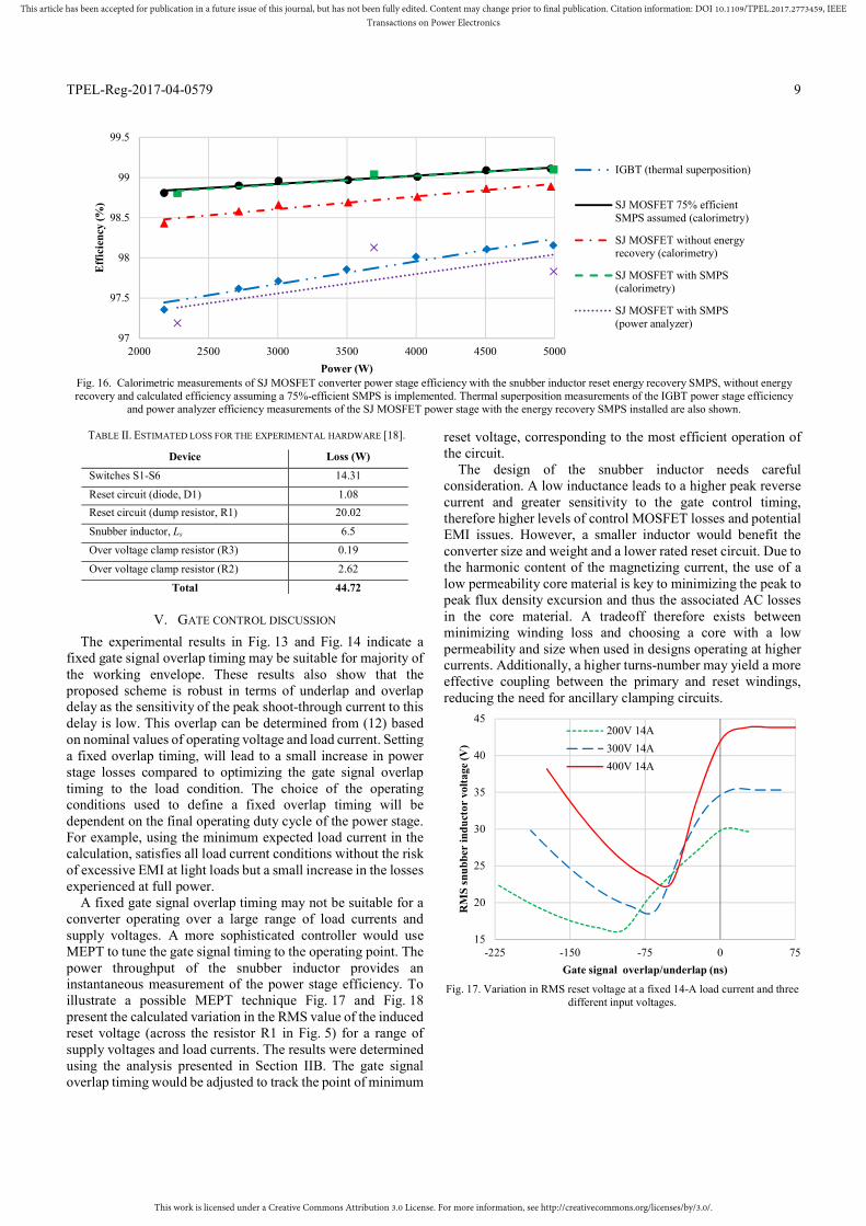
The converter power stage losses were measured operating from a 400-V supply voltage and increasing output loads at approximately 500-W increments between 2 kW and 5 kW through adjustment of the duty cycle. The switching overlap time was set to the optimal value of 50 ns as determined in Fig. 14. The results of the calorimetric efficiency measurements are given in Fig. 16. The efficiency, 𝜂, was determined by:
𝜂 =
𝑊 − 𝑊
𝑊 , (16)
where 𝑊 is the measured loss and 𝑊 is the input power measured using a power analyzer. 𝑊 was calculated using:
𝑊 = 𝑊 + 𝑊 (1 − 𝜂 ) (17)
In (17) 𝑊 is the dissipated power measured through calorimetry, 𝑊 is determined from (15) (dissipated externally to the calorimeter) and 𝜂 is the efficiency of a snubber inductor reset energy recovery SMPS circuit which was assumed to be 75%. This was verified through further calorimetric measurements of the power stage with the implemented demonstrator recovery SMPS at three load points as shown in Fig.16. Comparable efficiency figures derived from power analyzer power measurements at the same three loads are also shown, highlighting the inaccuracy of this approach. An efficiency of 99.1% was recorded at the rated 5-kW output and equated to 44 W (+/-0.5 W) of loss in the converter power stage (𝑊 = 39 W, 𝑊 = 20 W and 𝜂 = 0.75).
Benchmark efficiency measurements of the IGBT variant of the circuit, measured through thermal superposition, are also shown in Fig. 16. At full load, the SJ MOSFET power stage shows an efficiency improvement of 0.9% (with energy recovery) equating to a reduction in power stage losses of 47 W.
The full load efficiency determined through calorimetry as shown in Fig. 16 is similar to that determined from thermal superposition [18]. In [18], the estimated loss breakdown for the SJ MOSFET power stage was presented and is shown in Table II. The switching device losses were determined through thermal superposition, the reset and clamp circuit components through electrical measurement and the snubber inductor losses were pessimistically estimated by modelling the snubber inductor volume and its average measured temperature using finite element analysis. A 14-W difference can be observed between the loss figures derived from the two loss measurement techniques. This variation is due to a combination of factors; the accuracy of the loss measurement through calorimetry is higher than through thermal superposition, the minor losses in the auxiliary components were difficult to assess electrically and for the calorimetric loss measurement, the gate resistance for the upper devices in the bridge leg were increased to 18 Ω leading to inevitably higher switching losses.
This work is licensed under a Creative Commons Attribution 3.0 License. For more information, see http://creativecommons.org/licenses/by/3.0/.
This article has been accepted for publication in a future issue of this journal, but has not been fully edited. Content may change prior to final publication. Citation information: DOI 10.1109/TPEL.2017.2773459, IEEETransactions on Power Electronics
TPEL-Reg-2017-04-0579 9
TABLE II. ESTIMATED LOSS FOR THE EXPERIMENTAL HARDWARE [18].
Device Loss (W)
Switches S1-S6 14.31
Reset circuit (diode, D1) 1.08
Reset circuit (dump resistor, R1) 20.02
Snubber inductor, Ls 6.5
Over voltage clamp resistor (R3) 0.19
Over voltage clamp resistor (R2) 2.62
Total 44.72
V. GATE CONTROL DISCUSSION
The experimental results in Fig. 13 and Fig. 14 indicate a fixed gate signal overlap timing may be suitable for majority of the working envelope. These results also show that the proposed scheme is robust in terms of underlap and overlap delay as the sensitivity of the peak shoot-through current to this delay is low. This overlap can be determined from (12) based on nominal values of operating voltage and load current. Setting a fixed overlap timing, will lead to a small increase in power stage losses compared to optimizing the gate signal overlap timing to the load condition. The choice of the operating conditions used to define a fixed overlap timing will be dependent on the final operating duty cycle of the power stage. For example, using the minimum expected load current in the calculation, satisfies all load current conditions without the risk of excessive EMI at light loads but a small increase in the losses experienced at full power.
A fixed gate signal overlap timing may not be suitable for a converter operating over a large range of load currents and supply voltages. A more sophisticated controller would use MEPT to tune the gate signal timing to the operating point. The power throughput of the snubber inductor provides an instantaneous measurement of the power stage efficiency. To illustrate a possible MEPT technique Fig. 17 and Fig. 18 present the calculated variation in the RMS value of the induced reset voltage (across the resistor R1 in Fig. 5) for a range of supply voltages and load currents. The results were determined using the analysis presented in Section IIB. The gate signal overlap timing would be adjusted to track the point of minimum
reset voltage, corresponding to the most efficient operation of the circuit.
The design of the snubber inductor needs careful consideration. A low inductance leads to a higher peak reverse current and greater sensitivity to the gate control timing, therefore higher levels of control MOSFET losses and potential EMI issues. However, a smaller inductor would benefit the converter size and weight and a lower rated reset circuit. Due to the harmonic content of the magnetizing current, the use of a low permeability core material is key to minimizing the peak to peak flux density excursion and thus the associated AC losses in the core material. A tradeoff therefore exists between minimizing winding loss and choosing a core with a low permeability and size when used in designs operating at higher currents. Additionally, a higher turns-number may yield a more effective coupling between the primary and reset windings, reducing the need for ancillary clamping circuits.
Fig. 17. Variation in RMS reset voltage at a fixed 14-A load current and three
different input voltages.
15
20
25
30
35
40
45
-225 -150 -75 0 75
RM
S sn
ubb
er in
duct
or v
olta
ge (V
)
Gate signal overlap/underlap (ns)
200V 14A
300V 14A
400V 14A
97
97.5
98
98.5
99
99.5
2000 2500 3000 3500 4000 4500 5000
Eff
icie
ncy
(%)
Power (W)
IGBT (thermal superposition)
SJ MOSFET 75% efficientSMPS assumed (calorimetry)
SJ MOSFET without energyrecovery (calorimetry)
SJ MOSFET with SMPS(calorimetry)
SJ MOSFET with SMPS(power analyzer)
Fig. 16. Calorimetric measurements of SJ MOSFET converter power stage efficiency with the snubber inductor reset energy recovery SMPS, without energy recovery and calculated efficiency assuming a 75%-efficient SMPS is implemented. Thermal superposition measurements of the IGBT power stage efficiency
and power analyzer efficiency measurements of the SJ MOSFET power stage with the energy recovery SMPS installed are also shown.

This work is licensed under a Creative Commons Attribution 3.0 License. For more information, see http://creativecommons.org/licenses/by/3.0/.
This article has been accepted for publication in a future issue of this journal, but has not been fully edited. Content may change prior to final publication. Citation information: DOI 10.1109/TPEL.2017.2773459, IEEETransactions on Power Electronics
TPEL-Reg-2017-04-0579 10
Fig. 18. Variation in RMS reset voltage at a fixed 400-V input voltage and three different load currents.
VI. CONCLUSION
The paper has presented an approach for achieving very high converter efficiencies, at the operating voltages and powers found in applications such as domestic renewable energy systems and electric vehicles where efficiency of power conversion is paramount. 99.1% DC-DC conversion (excluding the input capacitor bank, output LC filter and gate drivers) has been demonstrated, verified through calorimetry, and assessed between 2 and 5-kW output to evaluate the concepts presented in this paper. High efficiencies have been attained by exploiting the beneficial conduction loss characteristics of SJ MOSFETs whilst overcoming their adverse switching characteristics at high voltage.
Through the use of a snubber inductor and gate signal overlap optimization, SJ MOSFETs have been shown to offer an attractive alternative to IGBTs and wide bandgap devices at this voltage and power level. In converters operating over a narrow range of load currents and operating powers, a fixed overlap has been shown to offer the most efficient and reliable technique to achieve very high efficiencies. However, if the range of operating load currents is large, a MEPT strategy may offer important system-level benefits, although additional control circuitry would be required. A loss vs. duty function has been experimentally determined that can be used to determine switching delay times in a system with MEPT.
Compared to an equivalent IGBT based power stage the proposed SJ MOSFET based circuit has resulted in a loss reduction of approximately 50%. As a result, the heatsink required for the SJ MOSFETs circuit would be considerably smaller and leads to a compact converter which can be cooled through natural convection. For example, if the IGBT variant of the power stage was required to operate under natural convection, increased converter cost and volume would be experienced leading to a significant gravimetric power density decrease (12.8kW/kg for the SJ MOSFET converter power stage and 2.4kW/kg for the IGBT based power stage assuming 5 kW operation and a suitably sized heatsink were implemented in each case). Alternatively, the application of forced cooling
methods lead to greater system losses, cost, complexity and volume.
VII. REFERENCES
[1] A. Claudio, M. Cotorogea, and J. Macedonio, “Comparative analysis of SJ-MOSFET and conventional MOSFET by electrical measurements,” Technical Proceedings, IEEE Int. Power Electron. Congr., Guadalajara, Mexico, pp. 96-100, Oct. 2002.
[2] G. Deboy, N. Marz, J.-P. Stengl, H. Strack, J. Tihanyi, and H. Weber, “A new generation of high-voltage MOSFET's breaks the limit line of silicon,” IEDM Tech. Dig., San Francisco, CA, USA, pp. 683–685, 1998.
[3] L. Lorenz, G. Deboy, A. Knapp, and M. Marz, “COOLMOSTM-a new milestone in high voltage power MOS,” in Proc., 11th Int. Symp. on Power Semiconductor Devices ICs (ISPSD’99), Toronto, Ont., Canada, pp. 3-10, May 1999.
[4] TK62J60W datasheet [Online], available www.toshiba.semicon-storage.com, accessed Oct. 2014.
[5] “650V Fast Recovery SuperFET ® II MOSFET Technology”, [Online], available: www.fairchildsemi.com, accessed Oct. 2016.
[6] B. Chen, B. Gu, L. Zhang, Z. U. Zahid, J.-S. Lai, and Z. Liao, “A high-efficiency MOSFET transformerless inverter for nonisolated microinverter applications,” IEEE Trans. Power Electron., vol. 30, no. 7, pp. 3610–3622, Jul. 2015.
[7] O. Alatise, N.-A. Adotei, and P. Mawby, “Super-junction trench MOSFETs for improved energy conversion efficiency,” in Proc., IEEE 2nd PES Int. Conf. and Exhibition on Innovative Smart Grid Technology (ISGT), Manchester, UK, Dec. 2011.
[8] R. Miftakhutdinov, “New ZVS analysis of PWM converters applied to super-junction, GaN and SiC power FETs,” in Proc., IEEE Appl. Power Electron. Conf. and Expo., Charlotte, NC, USA, pp. 336-341, Mar. 2015.
[9] R. Ouaida, M. Berthou, J. León, X. Perpiñà, S. Oge, P. Brosselard, and C. Joubert, “Gate oxide degradation of SiC MOSFET in switching conditions,” IEEE Electron. Device Letts., vol. 35, no. 12, pp. 1284–1286, Oct. 2014.
[10] D. B. DeWitt, C. D. Brown, and S. M. Robertson, “System and method for reducing body diode conduction,” US Patent No. 7508175 (B2), 24 Mar. 2009.
[11] W. Yu, H. Qian, and J.-S. Lai, “Design of high-efficiency bidirectional DC-DC converter and high-precision efficiency measurement,” in Proc., IEEE 34th Annu. Ind. Electron. Conf., Orlando, FL, USA, pp. 685-690, Nov. 2008.
[12] W. Guo, H. Bai, G. Szatmari-voicu, A. Taylor, J. Patterson, and J. Kane, “A 10kW 97 % -efficiency LLC resonant DC/DC converter with wide range of output voltage for the battery chargers in plug-in hybrid electric vehicles,” in Proc., IEEE Transportation Electrification Conf. and Expo (ITEC), Dearborn, MI, USA, pp. 1-4, Jun. 2012.
[13] S. Chen, D. Xiang, H. Wang, K. Tabira, and Y. Niimura,“Advantage of super junction MOSFET for power supply application,” in Proc., International Power Electron. and Appl. Conf. and Expo., Shanghai, China, pp. 1388-1392, Nov. 2014.
[14] T. Reiter, D. Polenov, H. Pröbstle, and H.-G. Herzog, “Observer based PWM dead time optimization in automotive DC/DC-converters with synchronous rectifiers,” in Proc., IEEE 39th Power Electron. Specialists Conf., Rhodes, Greece, pp. 3451-3456, Jun. 2008.
[15] T. Reiter, D. Polenov, H. Probstle, and H. G. Herzog, “PWM dead time optimization method for automotive multiphase DC/DC-Converters," IEEE Trans. Power Electron., vol. 25, no.6, pp. 1604-1614, Jun. 2010.
[16] M. Conrad and R. W. Dedoncker, “Avoiding reverse recovery effects in super junction MOSFET based half-bridges,” in Proc., IEEE 6th Int. Symp. on Power Electron. for Distributed Generation Systems, Aachen, Germany, pp. 1-5, Jun. 2015.
[17] B. Gu, J. Dominic, J. -S. Lai, C. -L. Chen, T. LaBella, and B. Chen, “High reliability and efficiency single-phase transformerless inverter for grid-connected photovoltaic systems,” IEEE Trans. Power Electron., vol. 28, no. 5, pp. 2235–2245, May 2013.
[18] A. Hopkins, N. McNeill, P. Anthony, and P. Mellor, “High efficiency bidirectional 5kW DC-DC converter with super-junction MOSFETs
20
25
30
35
40
45
50
-200 -150 -100 -50 0 50 100
RM
S sn
ubb
er in
duc
tor
volt
age
(V)
Gate signal overlap/underlap (ns)
400V 22A
400V 18A
400V 16A

This work is licensed under a Creative Commons Attribution 3.0 License. For more information, see http://creativecommons.org/licenses/by/3.0/.
This article has been accepted for publication in a future issue of this journal, but has not been fully edited. Content may change prior to final publication. Citation information: DOI 10.1109/TPEL.2017.2773459, IEEETransactions on Power Electronics
TPEL-Reg-2017-04-0579 11
for electric vehicle super-capacitor systems,” in Proc., IEEE 7th Energy Conversion Congr. and Expo., Montreal, QC, Canada, pp. 4632-4639, Sep. 2015.
[19] N. McNeill, P. Anthony, and N. Oswald, “Ultra-high efficiency machine drive inverter using super-junction MOSFETs,” in Proc., IET 7th Power Electron., Machines and Drives Conf., Manchester, UK, Apr. 2014.
[20] A. Hopkins, N. McNeill, P. Anthony, and P. Mellor, “Figure of merit for selecting super-junction MOSFETs in high efficiency voltage source converters,” in Proc., IEEE 7th Energy Conversion Congr. and Expo., Montreal, QC, Canada, pp. 3788-3793, Sep. 2015.
[21] Engauge digitiser program version 5.1 [Online], available: digitizer.sourceforge.net, accessed Dec. 2014.
[22] T130-6 Material datasheet [Online], available: www.micrometals.com, accessed Oct. 2014.
[23] R. Prieto, V. Bataller, J. A. Cobos, and J. Uceda, “Influence of the winding strategy in toroidal transformers,” in Proc., IEEE 24th Annu. Ind. Electron. Society Conf. (IECON '98), Aachen, Germany, vol. 1, pp. 359-364, Aug./Sep. 1998.
[24] Y. Fang, X. Ma, and Y. Xing, “Study on PV micro-inverter with coupled inductors and double boost topology,” in Proc., IEEE 7th Conf. on Ind. Electron. and Appl., Singapore, 2012, pp. 2054-2058.
[25] “Understanding diode reverse recovery and its effect on switching losses”, [Online], available: www.fairchildsemi.com, accessed Oct. 2016.
[26] IKW20N60T datasheet [Online], available: www.infineon.com, accessed Dec. 2014.
[27] C. Xiao, G. Chen, and W. G. H. Odendaal, “Overview of power loss measurement techniques in power electronics systems,” IEEE Trans. Ind. Appl., vol. 43, no. 3, pp. 657–664, May/Jun. 2007.
[28] D. Christen, U. Badstuebner, J. Biela, and J. W. Kolar, “Calorimetric power loss measurement for highly efficient converters,” in Proc., 2010 Int. Power Electron. Conf. (IPEC), Sapporo, Japan, pp. 1438–1445, Jun. 2010.
[29] N. Simpson and A. N. Hopkins, “An accurate and flexible calorimeter topology for power electronic system loss measurement,” in Proc., IEEE Int. Electric Machines and Drives Conf., Miami, FL, USA, May 2017.
Andrew N. Hopkins (M’16) received the M.Eng. degree in electrical and electronic engineering from the Department of Electrical and Electronic Engineering, University of Bristol, Bristol, U.K. in 2013. He is currently working toward the Ph.D. degree in power electronics with the Electrical Energy Management Research Group at the University of Bristol.
His research interests include calorimetry and high-efficiency power conversion for automotive applications.
Plamen Proynov received the B.Sc. (2005) and M.Sc. (2008) degrees in automation and control engineering from the University of Varna, Bulgaria. In 2014 he obtained his PhD degree at the University of Bristol, UK. His research was on the topic of power electronics for energy harvesting. Following his PhD he became a research associate at the
Electrical Energy Management Group at the University of Bristol, UK. As a research associate he worked on the SPHERE project investigating energy harvesting and wireless power transfer for domestic healthcare applications. His research
interests include low-power control strategies for power electronics, energy harvesting, and wireless power transfer.
Neville McNeill received the M.Phil. and Ph.D. degrees in power electronics from Napier University, Edinburgh, Scotland, in 2003 and 2008 respectively.
His career has included periods working for electric vehicle and renewable energy companies. From 2004 to 2016 he was at the University of Bristol, Bristol, U.K., where he was
latterly Senior Lecturer in Power Electronics. Since 2016 he has been with the Power Electronics, Drives and Energy Conversion (PEDEC) group in the Department of Electronic and Electrical Engineering at the University of Strathclyde, Glasgow, U.K. where he is Senior Research Fellow in Power Electronics. His main research interests are in high-efficiency multi-kilowatt power electronic conversion for aerospace, renewable energy, and electric vehicle applications.
Dr McNeill is a Member of the Institution of Engineering and Technology, a Chartered Engineer with the Engineering Council of the U.K., and a Fellow of the Higher Education Academy.
Bernard H. Stark received the M.S. degree in electrical engineering from the Swiss Federal Institute of Technology (ETH), Zurich, in 1995 and the Ph.D. degree in engineering from Cambridge University, U.K., in 2000.
He spent time as a Junior Research Fellow at St. Hugh’s College, Oxford, U.K., and as a member of the Control and
Power Group, Imperial College, London, U.K. He is currently Reader in Electrical and Electronic Engineering at the University of Bristol, and a member of the Electrical Energy Management Research Group. His research interests include renewable power sources and power electronics.
Phil H. Mellor (M’13) received the B.Eng. and Ph.D. degrees in electrical engineering from the Department of Electrical Engineering, University of Liverpool, Liverpool, U.K., in 1978 and 1981, respectively. He is currently a Professor of Electrical Engineering with the Department of Electrical and Electronic Engineering, University of
Bristol, Bristol, U.K. Prior to this, he held academic posts at the University of Liverpool from 1986 to1990 and the University of Sheffield, Sheffield, U.K., from 1990 to 2000. His research interests include high-efficiency electric drives, and actuation and generation systems for application in more electric aircraft and hybrid electric vehicles.


![Defenders of Ultramar [Graham McNeill]](https://img.pdfslide.us/doc/110x75/548d51c0b47959fa798b476b/defenders-of-ultramar-graham-mcneill.jpg)