Embed Size (px)
Citation preview
1
University of Technology, Sydney PO Box 123 Broadway NSW 2007 Australia
UTS School of Physics and Advanced Materials
Honours 2014
C09035 Bachelor of Science (Honours) in Applied Physics
C09046 Bachelor of Science (Honours) in Nanotechnology
Honours Webpage:
http://www.uts.edu.au/future-students/science/go-further/honours-program/school-physics-and-
advanced-materials

2
Table of Contents
1. General Information ....................................................................................................... 3
1.1 Message from the Head of School .......................................................................... 3
1.2 The Honours Year................................................................................................... 4
1.3 Research Project .................................................................................................... 4
1.4 Working as a Demonstrator .................................................................................... 4
1.5 Honours Eligibility ................................................................................................... 5
1.6 Honours Assessment .............................................................................................. 5
1.7 Meet our students ................................................................................................... 5
1.8 Contact Information ................................................................................................. 6
1.9 Applying for Honours .............................................................................................. 7
2. Research Projects by Supervisor................................................................................ 8

3
1. General Information
1.1 Message from the Head of School
Many years ago I completed an Honours project with a group of High Energy Physicists who were working on the predecessor to the LHC. I worked on refining the design of a cosmic ray telescope. However, more important than the details of the intensity spectrum of cosmic muons, I learned a huge amount about the conduct of science and the scientific workplace. Your Honours year marks a significant point in your education. It is an opportunity for you to push forward the boundaries of knowledge and for you to stretch out and expand your skills — skills that put you ahead wherever your future lies. It’s about advanced knowledge and application; relevant not only to those looking for a career in research, but to anyone looking to build work-relevant skills. We are fortunate in the School of Physics and Advanced Materials (PAM) to have access to cutting edge technology and academic leaders that can mentor and support you as a research student. You can talk to me, potential supervisors and particularly Matthew Arnold, your Honours co-ordinator and find out what’s involved in honours and how Honours can help you get ahead in a competitive job market. Congratulations on thinking about this exciting step and I hope we are a part of your endeavours in 2014. This booklet is designed to provide you with information about Honours in the School of PAM. Importantly it will introduce to the School, the Honours programs, the research projects on offer and who to talk to further about your future. Kendal McGuffie Head of School Physics and Advanced Materials [email protected]

4
1.2 The Honours Year
The PAM Honours program is a one year course (full-time) and consists of a research project and two course-work subjects. The research project spans across two semesters and the two course-work subjects are separate. The research project aims to develop students’ capability to undertake a guided program of scientific research in an area of physics or nanotechnology, from planning to execution. Honours projects in Applied Physics place a strong emphasis on applications of physics principles and methodologies. Nanotechnology projects often involve a number of different disciplines and the use of various techniques and instrumentation in diverse scientific fields. The aim of the course work is to develop students’ awareness of, and competency in, the advanced scientific concepts and theory that underlie modern physics and technology of materials. Topics will be treated more comprehensively and in greater depth than in the undergraduate course. Topics are determined by the expertise of lecturing staff in areas such as molecular dynamics, advanced microscopy, surface science, nanomaterials synthesis and characterisation, analysis of optical systems using matrix methods, electromagnetism, and advanced spectroscopic and vacuum techniques.
1.3 Research Project
The project consists of a literature review, development and enunciation of a research plan, and hands-on research work. This component is conducted at UTS, or jointly with an external partner, for example CSIRO or National Measurement Institute. Students will discuss a detailed project proposal with their supervisor(s) before starting the project and reach a clear agreement over the expected aims and outcomes of the project. In the first semester of study students are required to develop the literature review and research plan, and to gain experience in the research methods and techniques relevant to their project. In the second semester, students are required to implement the aims of the research and to evaluate the outcomes. Students need to aim to complete the research project by no later than early October in time for thesis submission and the final seminar. The student’s work in the research component of the degree is guided by the supervisor(s). The form of guidance can vary between projects but typically is provided at regular progress meetings between the student and supervisor.
1.4 Working as a Demonstrator
To help students in their Honours year the School offers an opportunity to undertake paid work as a demonstrator. As a demonstrator you will build your scientific, communication, presentation and teaching skills as well as earn money working on the UTS campus. Once approved as a demonstrator you will be guaranteed employment of least 2.5 hours a week for 7 weeks and will be paid at the attractive casual academic rate. Subsequent employment will be offered to interested students based upon performance.
5
1.5 Honours Eligibility
To be eligible for entry into a UTS Science Honours degree, applicants should have a Bachelor of Science degree in one of the following degrees and have achieved at least a credit average (≥ 65) over the final year (3rd year) of their undergraduate program.
Bachelor of Science in Applied Physics, or Bachelor of Science in Nanotechnology, or Bachelor of Science degree where appropriate science subjects have been taken.
1.6 Honours Assessment
Honours Assessment The overall research component conducted across the two semesters is assessed by a committee with input from at least three academics or external experts. Assessment is based upon a written thesis, one end-of-semester seminar and a supervisor’s assessment of your project work. The course-work subjects are assessed by the usual means used for taught subjects, such as written reports, exam, oral presentation and take-home assignments. The breakdown of assessment for the entire Honours year is as follows:
1. Research project 75% 2. Advanced Physics 12.5% 3. Advanced Nanomaterials 12.5%
____________________ Total 100% Honours Grading The Honours Committee will recommend the grade of Honours. The grades will be based on the weighted average mark awarded at the end of the Honours year.
• 85% - 100% First Class • 75% - 84% Second Class, Upper Division • 65% - 74% Second Class, Lower Division • 50% - 64% Third Class • < 50% Fail
Honours graduates with an exceptional undergraduate record and Honours mark may be eligible for the award of the University Medal.
1.7 Meet our students
We’ve asked some of our students to share their reasons for doing Honours and what their
experience has been so far.

6
Shane Ullman and Daniel Golestan – Honours students 2011
Shane Ullman Honours Thesis Topic: Kinetic Monte Carlo modelling of growth in obliquely deposited nanostructures
With Honours you have independence and while that is daunting it is really good – it really is
the next big step in our lives. PAM is a very close knit community which is great. We have
the opportunity to get to know each other and the academics. Friday night drinks are always
good.
Daniel Golestan Honours Thesis Topic: Investigating trapping levels in wide bandgap semiconductors
It is a fundamental part of the human condition to find out about the world around you. Since
I was a child I was always curious so it was logical that I would be interested in science. We
have a tradition this year of having talks every few weeks in the MAU with beer and pizza. It
is a good tradition and helps with my project as I get to air any concerns which the whole
school can talk about.
1.8 Contact Information
Name and Position Room Ext (phone)
Faculty and School Staff
Bruce Milthorpe Dean of Science
CB04.04.48h Katherine Walsh (Executive Assistant) Email: [email protected] Phone: 9514 1752
Greg Skilbeck Associate Dean (Research)
CB04.04.48i x1760 [email protected]
Kendal McGuffie Head of School PAM
CB01.12.27 X2072 [email protected]
Matthew Arnold Honours Coordinator PAM
CB01.12.33 X9715 [email protected]
Katie McBean Professional Officer Operations
CB04.1.37 x7817 [email protected]
7
1.9 Applying for Honours
Look View the list of Honours projects available in 2014. Talk Talk to supervisors about the projects you are interested in. You are strongly encouraged to have discussions with several possible supervisors before choosing a project. It is important to choose a project and supervisor to suit your interests and skills. Speaking to current Honours and postgraduate students will also give you valuable feedback. Apply
Download and complete a UTS Direct Application Form Autumn 2014 for admission to do honours at UTS.
You will also need to submit a Faculty of Science Supplementary Application Form. Your preferred supervisor should also complete and sign the appropriate page.
Submit both forms to the Student Centre by 29 November 2013.
8
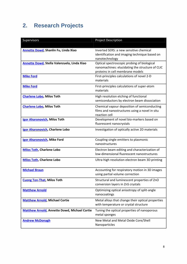
2. Research Projects
Supervisors Project Description
Annette Dowd, Shanlin Fu, Linda Xiao Inverted SERS: a new sensitive chemical identification and imaging technique based on nanotechnology
Annette Dowd, Stella Valenzuela, Linda Xiao Optical spectroscopic probing of biological nanomachines: elucidating the structure of CLIC proteins in cell membrane models
Mike Ford First-principles calculations of novel 2-D materials
Mike Ford First-principles calculations of super-atom materials
Charlene Lobo, Milos Toth High resolution etching of functional semiconductors by electron beam dissociation
Charlene Lobo, Milos Toth Chemical vapour deposition of semiconducting films and nanostructures using a novel in situ reaction cell
Igor Aharonovich, Milos Toth Development of novel bio-markers based on fluorescent nanocrystals
Igor Aharonovich, Charlene Lobo Investigation of optically active 2D materials
Igor Aharonovich, Mike Ford Coupling single emitters to plasmonic nanostructures
Milos Toth, Charlene Lobo Electron beam editing and characterization of low-dimensional fluorescent nanostructures
Milos Toth, Charlene Lobo Ultra-high resolution electron beam 3D printing
Michael Braun Accounting for respiratory motion in 3D images using partial volume correction
Cuong Ton-That, Milos Toth Structural and luminescent properties of ZnO conversion layers in ZnS crystals
Matthew Arnold Optimizing optical anisotropy of split-angle nanocoatings
Matthew Arnold, Michael Cortie Metal alloys that change their optical properties with temperature or crystal structure
Matthew Arnold, Annette Dowd, Michael Cortie Tuning the optical properties of nanoporous metal sponges
Andrew McDonagh New Metal and Metal Oxide Core/Shell Nanoparticles
9
Inverted SERS: a new sensitive chemical identification and imaging technique based on
nanotechnology
Dr Annette Dowd, Dr Shanlin Fu, Dr Linda Xiao
There is a great need for sensitive identification and mapping of trace quantities of hazardous
substances on objects. Raman spectroscopy has been developed into a useful technique for hazard
identification but it is limited by its sensitivity. Surface enhanced Raman Spectroscopy (SERS), based
on the interaction of light, metal nanostructures and the substance of interest, has been used to
greatly increase the chemical sensitivity of the technique by many orders of magnitude.
Unfortunately this technique currently involves removing the hazardous substance from the object
and/or destroying the object before SERS can be performed and imaging is impossible.
The aim of this project is to develop a new, simple SERS protocol where the metal nanoparticles are
deposited at high density directly onto the object, without the need to remove the hazardous
substance, i.e. an inverted SERS protocol. The potential of this technique for micron-resolution SERS
imaging of the contaminant distribution on the otherwise unaltered object will also be tested.
This multidisciplinary project will be undertaken both in PAM and CFS laboratories. Opportunities
will be available to access state-of-the-art equipment with collaborators at the Vibrational
Spectroscopy Facility at the University of Sydney.
(http://sydney.edu.au/science/chemistry/spectroscopy/index.shtml)
Techniques: Raman spectroscopy, Confocal microscopy, Magnetron sputtering, nanoparticle
synthesis, microspectrophotometry, SEM, perhaps multivariate data analysis depending on interest
of student.
Suitable for: Honours (Nanotechnology or Physics)
10
Optical spectroscopic probing of biological nanomachines: elucidating the structure of
CLIC proteins in cell membrane models
Dr Annette Dowd, A/Prof Stella Valenzuela, Dr Linda Xiao
Raman spectroscopy is a potentially powerful tool to monitor modification in the lipid bilayer and
also the protein structure. Characteristic vibrations of chemical bonds can be subtly changed by their
nanoscale local environment, e.g. the frequency associated with the peptide bond depends on
whether it is situated in an alpha-helix or a beta-sheet structure. Raman spectroscopy can
interrogate these chemical bonds in a noninvasive way by using only a tightly focused laser beam.
The aim of this project is to add to knowledge about the structure of the CLIC protein machinery and
its insertion into lipid bilayer membranes using a novel application of Raman microspectroscopy.
This student will study the effect of cholesterol on the lipid structure, protein structure and its
insertion. The student will also develop the Raman technique by investigating different types of
membrane preparation (liposomes, single tethered layers etc) and the use of nanostructured SERS
substrates for signal enhancement.
This multidisciplinary project will be undertaken in PAM, CFS and MMB laboratories. Opportunities
will be available to access state-of-the-art equipment with collaborators at the Vibrational
Spectroscopy Facility at the University of Sydney.
(http://sydney.edu.au/science/chemistry/spectroscopy/index.shtml)
Techniques: Raman spectroscopy, Confocal microscopy, Magnetron sputtering, SEM, perhaps
multivariate data analysis depending on interest of student.
Suitable for: Honours (Nanotechnology or Physics)

11
First-principles calculations of novel 2-D materials
A/Prof Mike Ford
Graphene is the most famous 2-D material: a material that is one atom thick. Interest in Graphene
stems from its unusual properties, such as high mechanical strength and potential applications in
electronic devices. More recently other 2-D materials such as MoS2 have started to gain
prominence again because of unusual and potentially useful properties.
The aim of this project is to use computer simulations to investigate new 2-D materials that are yet
to be made experimentally. As suggested in a recent computational paper by Lebegue et al (Phys Rev
X, 3, pp031002, 2013) there are a number of transition metal dichalcogenides that are worth
exploring. Perhaps more interesting are hybrid layered structures that are composed of alternating
stacks of different 2-D materials, for example alternating layers of h-BN and graphene.
Techniques: Computer based materials simulations. We would most likely use the computer
packages VASP and SIESTA. These are both implementation of Density Functional Theory and solve
the Schroedinger equation. Depending upon interest there is also opportunity to write your own
codes for analysis of the data.
Suitable for: Honours (Nanotechnology or Physics)
12
First-principles calculations of super-atom materials
A/Prof Mike Ford
Conventional solid materials are made from collections of atoms, for example NaCl is binary solid
compound made up of Na and Cl atoms bound to each other due to charge transfer between the
two atoms forming ionic bonds.
Recently the first in a whole new class of solid-state materials was produced (Roy et al, Science 341,
pp157 2013). In this material clusters of atoms are the basic building blocks once again held
together by charge transfer and Van der Waals bonds. This opens up the possibility of creating
whole families of new materials where properties and functionality can be controlled by varying the
superatom building blocks.
In this project we will use computer simulations to look at the atomic properties of these new
materials. The starting point would be those few materials already successfully synthesised
experimentally, with the aim of predicting new super-atom materials.
Techniques: Computer based materials simulations. We would most likely use the computer
packages VASP and SIESTA. These are both implementation of Density Functional Theory and solve
the Schroedinger equation. Depending upon interest there is also opportunity to write your own
codes for analysis of the data.
Suitable for: Honours (Nanotechnology or Physics)

13
High resolution etching of functional semiconductors by electron beam dissociation
Charlene Lobo, Milos Toth
Electron beam induced deposition and etching (EBID and EBIE) are high resolution, direct write
techniques for the fabrication of functional nanostructures such as Au (for formation of
nanostructure contacts and plasmonic applications), SiO2 (for photomask repair) and Pt (for
catalysis), as well as etching of diamond, chrome, silicon and a host of other functional materials.
This project will develop new chemistries and processes for EBIE of semiconductor nanostructures
by dissociation of appropriate chemical etch precursors. Initial experiments will be performed in an
ex-situ reaction chamber supplied by industry partner FEI company (www.fei.com).
Successful etch chemistries will be applied to etching of ZnO nanowires, MoS2 and GaN
nanostructures, among other light-emitting semiconductors, thus providing a new method of
altering their bandgaps and light emission properties.
Techniques: Electron beam induced etching aided by compositional and surface characterisation
techniques available in the MAU, including photoelectron yield spectroscopy, mass spectroscopy,
and energy/wavelength dispersive X-ray spectroscopy.
Suitable for: Honours (Physics or Nanotechnology)

14
Chemical vapour deposition of semiconducting films and nanostructures using a novel in
situ reaction cell
Dr Charlene Lobo, Prof Milos Toth
This project will employ a novel in-situ reaction cell for the growth of functional thin films and
nanostructures (eg, narrow and wide bandgap semiconductors, and C nanotubes). The reaction cell
will be housed inside an ultra-high-resolution environmental scanning electron microscope equipped
with analysis techniques that enable high resolution imaging and analysis to be conducted in real
time during deposition. This state-of-the-art technology is unique to the MAU, as it employs the use
of future generation electron microscopy and chemistry hardware prototypes supplied by the high
tech industry collaborator FEI Company (www.fei.com).
Precursors available for nanostructure growth include SiCl4 and GeCl4 (for Si and Ge nanowires and
epilayers), and ethanol or benzene (for C nanotubes and graphene respectively). Time and resource-
permitting, precursors for the growth of GaN and ZnO will be investigated. Nanostructure growth
will be initiated using colloidal nanoparticles as catalyst seeds (eg, Au and Co colloids), while
epitaxial growth will be attempted on lattice-matched substrates. Growth conditions will be adapted
from prior work conducted using the same precursors in an ex-situ growth chamber, as well as from
the scientific literature.
Techniques: Growth by chemical vapour deposition, and surface and nanostructure characterisation
techniques available in the MAU, including ultra high-resolution electron microscopy,
cathodoluminescence, photoluminescence, photoelectron yield spectroscopy and residual gas
analysis.
Suitable for: Honours (Physics or Nanotechnology)

15
Development of novel bio-markers based on fluorescent nanocrystals
Dr Igor Aharonovich, Prof Milos Toth
The goal of the project is to demonstrate use of nanodiamonds as bio-markers for biological tagging
and labelling. Nanodiamonds are biocompatible and host bright color centers which can be used as
efficient bio labels.
The project will consist of two main steps: (1) synthesis and characterisation of small (sub 40 nm)
nanodiamonds that contain bright color centers. (2) Incorporation of the nanodiamonds into
biological media – e.g. cells. Several challenges will be addressed by the students during the project:
prevention of nanodiamonds’ agglomeration, investigation of emitter photostability in small
particles, characterization of nanodiamonds in cells.
This multidisciplinary project will provide the student exposure to both optical and biological
sciences. The student will have access to the newly established nanophotonics laboratory that
includes a confocal microscope for the photoluminescence measurements as well as the opportunity
to learn basic biological processes and work with cells.
Techniques: Confocal microscopy, Scanning Electron Microscopy, biological sample preparation.
Suitable for: Honours (Nanotechnology or Physics)

16
Investigation of optically active 2D materials
Dr Igor Aharonovich, Dr Charlene Lobo
Two dimensional materials (2D) such as graphene attract a lot of attention due to their unique
photophysical properties. Recently, it was shown that single layers of di-chalcogenides (MoS2/WS2)
are optically active materials that exhibit bright florescence.
This project will be focused on understanding the optical properties of these materials. The student
will investigate defect generation in these materials, perform high resolution spectroscopy and
measure photon statistics.
The student will have access to the materials and will investigate novel growth methods of single
layered materials. The newly established nanophotonics laboratory that includes all the required
optical gear (single photon detectors, spectrometer, low temperature cryostat etc) will be used for
characterization. The student will also get experience in nanomaterials characterization using SEM,
AFM and will pursue basic nanofabrication processes.
Techniques: Confocal microscopy, Scanning Electron Microscopy, chemical vapor deposition,
Cathodoluminescence, low temperature spectroscopy.
Suitable for: Honours (Nanotechnology or Physics), Engineering Capstone

17
Coupling single emitters to plasmonic nanostructures
Dr. Igor Aharonovich, A/Prof Mike Ford
The goal of the project is to develop robust methods to couple single emitters to plasmonic
nanostructures. One of the main challenges in single photon emitters is their relatively low
brightness. Through coupling to plasmonic resonators, the emission is enhanced and the excited
state lifetime is reduced.
The project will involve characterization of single photon emitters using a confocal microscope and
Hunbury Brown and Twiss interferometer. Once the emitters are selected, metal nanoparticles such
as gold and silver will be deterministically positioned in a close proximity to the emitters. To
optimize the coupling, various parameters including emitter’s distance, dipole orientation and the
plasmonic medium would be varied. If time permits, modeling of the system will be conducted to
understand the underlying photophysical processes.
The student will have access to the newly established nanophotonics laboratory that includes all the
required optical gear (single photon detectors, spectrometer, low temperature cryostat etc). The
student will also get experience in nanomaterials characterization using SEM, AFM and will pursue
basic nanofabrication processes.
Techniques: Confocal microscopy, Scanning Electron Microscopy, cathodoluminescence, low
temperature spectroscopy.
Suitable for: Honours (Nanotechnology or Physics), Engineering Capstone
18
Electron beam editing and characterization of low-dimensional fluorescent
nanostructures
Prof. Milos Toth, Prof. Matthew Phillips, Dr. Igor Aharonovich
Cathodoluminescence (CL) spectroscopy and imaging enables nano scale mapping of the
optoelectronic properties materials and devices. CL is performed using an electron beam which can
also be used to edit nanostructures. This project will use state-of-the-art CL models and/or
experiments to improve our understanding of the fundamental processes behind CL generation in
low-dimensional (i.e., 2D, 1D or 0D) nanostructures. Electron beam editing (modification) will be
used to verify and improve current understanding of cathodoluminescence generation in materials
excited by an electron beam.
The student will use a combination of theory and experiment, and will have the option to focus
primarily on computer modeling or experiments.
Techniques: High vacuum and gas-assisted electron microscopy, CL and basic computer models of CL
generation.
Suitable for: Honours (Nanotechnology or Physics), Engineering Capstone

19
Ultra-high resolution electron beam 3D printing
Prof. Milos Toth, Dr. Charlene Lobo
Gas-mediated Electron Beam Induced Etching and Deposition (EBIED) are direct write material
fabrication techniques with nanometer resolution. This project will identify fundamental
physicochemical mechanisms that limit EBIED resolution, and will develop techniques for direct
writing of functional 3D nanostructures that can't be realized by conventional EBIED strategies.
Initial experiments and/or computational modeling will be used to understand how EBIED 3D
printing resolution is affected by precursor supply kinetics. These results will then be used to design
EBIED strategies for fabrication of novel three-dimensional nanostructures for nano scale optical and
electronic devices.
The student will have the option to limit the project scope to experiments, computer simulations, or
a combination of both.
Techniques: Electron microscopy, EBIED, scanning probe microscopy and/or computer models of
EBIED. Optionally, a range of spectroscopic techniques may be used for characterization of EBIED-
grown nanostructures.
Suitable for: Honours (Nanotechnology or Physics), Engineering Capstone

20
Accounting for respiratory motion in 3D images using partial volume correction
Michael Braun
One of the most significant impediments to accurate diagnosis of lesions in thoracic organs is the
respiratory motion occurring during image acquisition. The motion can be frozen using breath-hold
in CT and MR imaging but not in noise-limited modalities, such as emission tomography (PET,
SPECT). For example, in PET gated cardiac studies, the cardiac image data are accumulated at
distinct intervals of the cardiac cycle, such as the peak of diastole or systole, using the ecg signal.
Thus the image data are synchronized with the cardiac cycle. However, the ecg gating ignores the
slower and much less regular respiratory motion. The result may be that the method of gathering
data for cardiac gated studies is compromised by the respiratory motion. The motion of the thorax
organs can be measured directly or deduced by monitoring external devices, such as an elastic belt
(Martinez-Möller et al, Eur J Nucl Med Mol Imaging 34(9):1447–1454, 2007). This project aims to
apply a model of respiratory motion to a simulation of cardiac PET study in order to analyze the
effect of respiratory motion. The project will then develop a method of correcting the effect in
clinical images by an adaptation of a partial volume correction algorithm.
The project will be carried out in collaboration with the Institute of Nuclear Medicine at the
University College London. The project will suit a student comfortable with computational
modelling (e.g. in Matlab) and interest in medical imaging.
Techniques: The student will be implementing modelling and developing a correction algorithm
using a scripting language, such as Matlab or IDL.
Suitable for: Honours (Nanotechnology or Physics)

21
Structural and luminescent properties of ZnO conversion layers in ZnS crystals
Cuong Ton-That, Milos Toth
ZnO and ZnS are important II-VI semiconductors with unique optoelectronic properties. Both are
well-known luminescent materials with a wide range of technological applications including light
emitting diodes, laser diodes and flat panel displays. Recently, fabrication of ZnO-ZnS
heterostructures with various morphologies has been reported. This project aims to fabricate ZnO
layers by partial conversion from ZnS crystals. In the first instance, thermal oxidation of ZnS by radio
frequency plasma or annealing in oxygen atmosphere will be investigated as a method for the
fabrication of a ZnO conversion layer. We will start by studying the effect of a range of processing
conditions on the properties of ZnO/ZnS structures. At a later stage, we will investigate fabrication of
ZnS-ZnO nanostructures using electron beam modification. Fabricated structures will be analysed by
x-ray diffraction, electron microscopy, cathodoluminescence and x-ray microanalysis to investigate
the relationship between structural and optical properties. Depth-resolved cathodoluminescence
will be used for depth profiling of luminescence centres in ZnS and ZnO.
Techniques: Plasma processing, electron microscopy, cathodoluminescence, x-ray diffraction, energy
dispersive x-ray analysis
Suitable for: Honours (Physics or Nanotechnology)

22
Optimizing optical anisotropy of split-angle nanocoatings
Matthew Arnold
Anisotropic optical coatings polarize light and have applications in areas such as display technology
and specialized imaging. Oblique deposition produces nanostructures with high anisotropy, which
can be further improved through dynamic rotation of the substrate during deposition. Shadowing
and diffusion have been identified as two key physical processes, but it is not clear how these
combine to increase anisotropy in this case.
The aim of this project is to test a new growth regime that may offer insight on the underlying cause
of increased anisotropy. Coatings will be deposited under different incident angles, the growth
characterized via SEM, and the permittivity tensor determined with ellipsometry. Data from the
new growth regime will be compared to existing models to identify any anomalies.
Techniques: PVD, ellipsometry, SEM, thin film models.
Suitable for: Honours (Nanotechnology or Physics), Engineering Capstone

23
Metal alloys that change their optical properties with temperature or crystal structure
Dr Matthew Arnold, Prof. M Cortie
The next generation of nanoscale optical devices, for example nano-antennas, will be fabricated
using various metallic elements (e.g. Au, Ag or Al) and, maybe, alloys or intermetallic compounds of
these or other elements. The dielectric function (a.k.a. 'refractive index') of these materials
determines how well they can perform in these applications. Here we are interested in the prospect
of developing alloys that will undergo a change in dielectric function as they are heated or cooled.
The alloy CuAu (also known as 'red gold') seems to have this property as might the shape memory
alloy Au7Cu5Al4 ('spangold'). Some special compositions of brass have also been reported to undergo
a colour change due to a change in intrinsic crystal structure. However, not much has been reported
in the scientific literature regarding these possibilities. The aims of the present project are (1) to find
out how much of a change in dielectric properties is possible, and (2) to find out whether any of the
alloys of the elements mentioned above might have useful optical properties.
Techniques: Scanning electron microscopy, UV-vis spectroscopy, ellipsometry, X-ray diffraction (and
numerical or mathematical methods associated with these techniques)
Suitable for: Honours (Nanotechnology or Physics), Engineering Capstone

24
Tuning the optical properties of nanoporous metal sponges
Dr Matthew Arnold, Dr Annette Dowd, Prof. M Cortie
The optical properties of nano- and meso-porous metal sponges are closely correlated with their
morphology. Sponges of this type can be made to exhibit a very flat spectral response over a broad
range of the optical spectrum. Metal sponges have some optical applications in scientific
instrumentation and are being considered as a substrate to provide Surface Enhanced Raman
spectroscopy. However, the sponge microstructure is metastable and it coarsens quite readily at
temperatures above ambient.
The aim of this project is to use a combination of ellipsometry, X-ray diffraction, electron microscopy
and computer modelling to study the coarsening process with a view to being able to control it.
Techniques: Scanning electron microscopy, UV-Vis spectroscopy, ellipsometry, X-ray diffraction (and
numerical or mathematical methods associated with these techniques)
Suitable for: Honours (Nanotechnology or Physics), Engineering Capstone
25
New Metal and Metal Oxide Core/Shell Nanoparticles
Dr A McDonagh
In this project, nanoparticles containing metal oxide cores coated with gold will be investigated. The
particles will then be examined by ablating them with a laser and analysing the masses of the
ablated materials under various conditions.
Nanoparticles made of gold have proven to be extremely valuable as probes to visualise important,
individual features within biological specimens. However, if multiple targets are to be imaged, then a
solid gold particle provides no means of distinguishing between the targets. As a solution to this
problem, core−shell structures may be used as extremely sensitive bio-imaging probes if they
possess an appropriate metal oxide core and gold shell.
This project will result in new nanoparticles and new knowledge about the laser ablation of the new
particles under various conditions. The particles may be applied to biological material to enable
imaging of molecule/particle interactions as well as their interaction with light.
Techniques: Nanoparticle synthesis, molecular synthesis, measurement of optical properties, laser
ablation, mass spectrometry.
Suitable for: Honours (Nanotechnology or Physics)