Embed Size (px)
Citation preview

92
Transactions of The Japan Institute of Electronics Packaging Vol. 5, No. 1, 2012
1. IntroductionMEMS devices such as piezoelectric devices are being
used for various purposes in recent years. In MEMS
device manufacturing, the diameter of the silicon wafer
used has been expanding in order to facilitate mass pro-
duction and cost reduction. Thin films, such as metal or
ferroelectric films, are produced on these large wafers and
devices are then formed using micromachining processes
like photolithography. However, it is very difficult to pre-
pare dielectric films with the requisite homogeneous thick-
ness and electrical properties on large wafers because of
problems such as residual stress,[1] and therefore, the
reliability of the devices deteriorates in the course of these
processes. Generally, physical vapor deposition (PVD),
such as sputtering, and metal organic chemical vapor
deposition (MOCVD) are said to be comparatively repro-
ducible when preparing dielectric film on large wafers, but
these methods require very expensive and large-scale
equipment such as vacuum systems. Therefore, metal
organic decomposition (MOD), a chemical solution depo-
sition (CSD) method, was used for the preparation of the
dielectric thin film in this study. Besides not requiring
expensive equipment, this method also has other advan-
tages in that large-area films can be obtained and the com-
position can be easily controlled. The MOD method, how-
ever, has problems of low homogeneity of the electrical
properties and the difficulty of controlling many process
parameters. Therefore, the objective of this study was to
solve these problems and apply this method to 4-inch
wafer film formation. We evaluate the significance of the
parameters and homogeneity of the film quantitatively for
this objective. In our experiments, we used lead zirconate
titanate (Pb(Zr,Ti)O3, PZT) as the dielectric film because it
is one of the most common materials used for MEMS
[Technical Paper]
Homogenizing and Applying Dielectric Film to Wafer-Level Film
PreparationKazutaka Sueshige*, Keita Iimura*, Masaaki Ichiki*,**,****, Tadatomo Suga*, and Toshihiro Itoh***,****
*Department of Precision Engineering, School of Engineering, University of Tokyo, 7-3-1 Hongo, Bunkyo-ku, Tokyo 113-8656, Japan
**JST-PRESTO, 7, Goban-cho, Chiyoda-ku, Tokyo 102-0076, Japan
***AIST, 1-2-1 Namiki, Tsukuba-shi, Ibaraki 305-8564, Japan
****JST-CREST, 7, Goban-cho, Chiyoda-ku, Tokyo 102-0076, Japan
(Received June 28, 2012; accepted November 8, 2012)
Abstract
MEMS devices such as piezoelectric devices are being used for various purposes in recent years. At the same time, sili-
con wafer diameters have been expanding for the purposes of mass production and cost reduction in the manufacture of
these devices. Therefore, it is becoming more difficult to prepare a dielectric film with homogeneous thickness and
electrical properties on the wafer. Generally, physical vapor deposition (PVD) methods such as sputtering are said to be
comparatively reproducible for preparing films on large wafers, but these methods require expensive equipment. Metal
organic decomposition (MOD), a chemical solution deposition (CSD) method, was used to form a PZT (Pb(Zr,Ti)O3) film
on the 4-inch wafers in this study because it does not need expensive equipment such as a vacuum system. To improve
the ferroelectric properties of the film formed using the MOD method, we optimized the process parameters using
design of experiments methods and found that temperature is the most significant control factor. A PZT film was prepared
homogeneously on 4-inch wafers under optimum conditions. Furthermore, a more homogeneous PZT film was prepared
by making the temperature uniform using a soaking cover. We think that these results can be applied to the preparation
of films on larger wafers as an alternative to PVD methods, which are currently the main method of preparing dielectric
films but which require expensive equipment.
Keywords: PZT, MOD, MEMS, Homogeneity, Ferroelectric
93
Sueshige et al.: Homogenizing Wafer Level Dielectric Film (2/7)
applications.[2]
2. Experiments2.1 Optimization of process parameters
The MOD process parameters were optimized by
design of experiments to improve the electrical properties
and the crystal orientation of the film. We also identified
significant parameters by analysis of variance. Design of
experiments and analysis of variance are statistical and
mathematical methods for conducting efficient experi-
ments and are used in various studies such as the optimi-
zation of sputtering or CVD conditions.[3–6] Using these
methods, we can not only optimize parameters but also
determine which parameter has the largest effect on prop-
erties.
First, a SiO2 film about 300 nm thick was formed on a
4-inch silicon wafer as an insulating layer using an oxida-
tion furnace. Then, Ti and Pt were sputtered as an adhe-
sion layer and a bottom electrode. The thicknesses of the
Ti and Pt were approximately 5 nm and 150 nm, respec-
tively. After sputtering, the 4-inch Pt/Ti/SiO2/Si substrate
was diced to 20 mm × 20 mm chips and these were ultra-
sonically cleaned in pure water, 2-propanol, and acetone. A
PZT film was then prepared on these substrates using the
MOD method, which consists of two processes: spin-coat-
ing, and rapid thermal annealing (RTA). First, the PZT
solution (Kojundo Chemical Co.), which consists of PbO,
ZrO2, TiO2 and organic solvent, was spin-coated at 2,500
rpm for 20 s. The molar ratio of PbO:ZrO2:TiO2 is 120:52:48
and the mass concentration of these oxides is 10% or 20%
in total. The sample was then annealed in air at 120°C for 2
min (evaporation of organic solvent), 250°C for 5 min (pre-
cursor formation) and 600°C or 700°C for 2 min (crystalli-
zation of the PZT). As shown in Table 1, three parameters
(the crystallization temperature in RTA, the heating rate in
RTA, and the mass concentration of the PZT solution)
were varied in these processes to optimize these parame-
ters. The spin-coating and RTA processes were repeated
ten times to prevent leaks in each experiment. The thick-
ness of the film using 10 wt% solution was 1.3 μm and that
using 20 wt% solution was 2.5 μm after 10 times coating.
After the PZT film was formed, each sample was etched
by a buffered hydrofluoric etchant to expose the bottom
electrode and Pt was sputtered for the top electrode. The
properties of each sample were then measured. The full
width at half maximum (FWHM) of the (100) peak of the
X-ray diffraction (XRD) pattern of the films was measured
to evaluate the crystal orientation. The dielectric constants
and P-E hysteresis loops of the films were also measured.
After that, the optimum conditions and significance of each
parameter were investigated using analysis of variance.
2.2 Wafer level film preparationNext, a PZT film was prepared on the 4-inch wafer under
optimum conditions, and the thickness and electrical prop-
erties were investigated to evaluate the homogeneity of
the film. The spin-coating and RTA processes were
repeated ten times. To measure the thickness and electri-
cal properties at various points on the film, holes were
made in the PZT film using photolithography and Pt was
sputtered using a metal mask. As shown in Fig. 1, the
holes are located at 10 mm intervals. The top electrodes
are also located at 10 mm intervals.
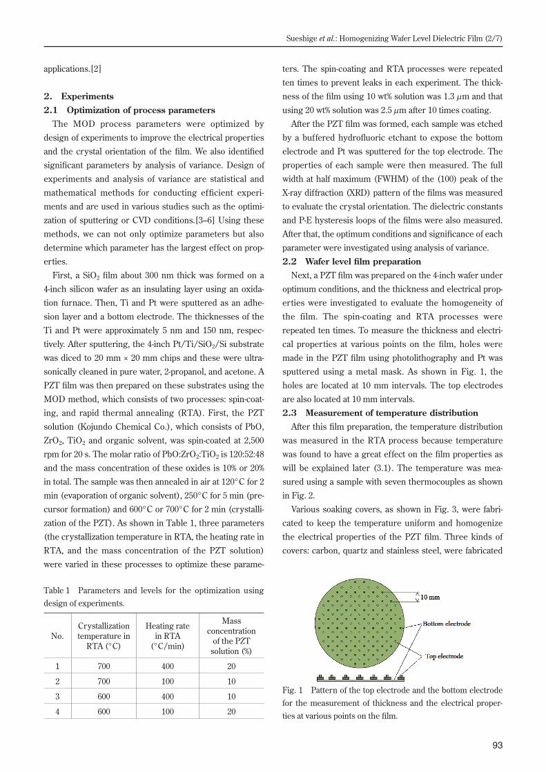
2.3 Measurement of temperature distributionAfter this film preparation, the temperature distribution
was measured in the RTA process because temperature
was found to have a great effect on the film properties as
will be explained later (3.1). The temperature was mea-
sured using a sample with seven thermocouples as shown
in Fig. 2.
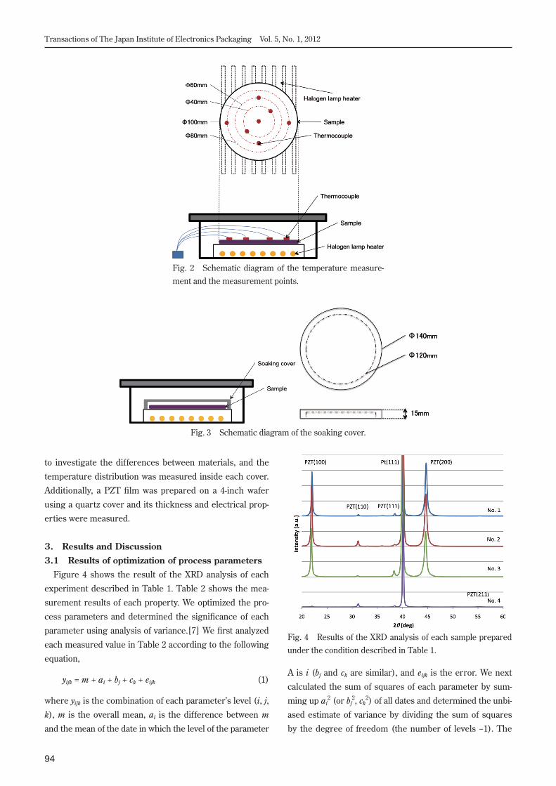
Various soaking covers, as shown in Fig. 3, were fabri-
cated to keep the temperature uniform and homogenize
the electrical properties of the PZT film. Three kinds of
covers: carbon, quartz and stainless steel, were fabricated
Table 1 Parameters and levels for the optimization using design of experiments.
No.Crystallization temperature in
RTA (°C)
Heating rate in RTA
(°C/min)
Mass concentration
of the PZT solution (%)
1 700 400 20
2 700 100 10
3 600 400 10
4 600 100 20
Fig. 1 Pattern of the top electrode and the bottom electrode for the measurement of thickness and the electrical proper-ties at various points on the film.
94
Transactions of The Japan Institute of Electronics Packaging Vol. 5, No. 1, 2012
to investigate the differences between materials, and the
temperature distribution was measured inside each cover.
Additionally, a PZT film was prepared on a 4-inch wafer
using a quartz cover and its thickness and electrical prop-
erties were measured.
3. Results and Discussion3.1 Results of optimization of process parameters
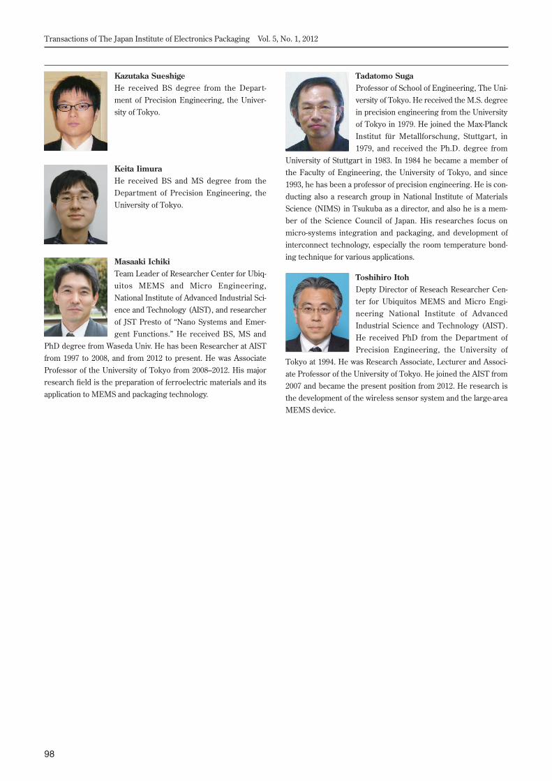
Figure 4 shows the result of the XRD analysis of each
experiment described in Table 1. Table 2 shows the mea-
surement results of each property. We optimized the pro-
cess parameters and determined the significance of each
parameter using analysis of variance.[7] We first analyzed
each measured value in Table 2 according to the following
equation,
yijk = m + ai + bj + ck + eijk (1)
where yijk is the combination of each parameter’s level (i, j,
k), m is the overall mean, ai is the difference between m
and the mean of the date in which the level of the parameter
A is i (bj and ck are similar), and eijk is the error. We next
calculated the sum of squares of each parameter by sum-
ming up ai2 (or bj
2, ck2) of all dates and determined the unbi-
ased estimate of variance by dividing the sum of squares
by the degree of freedom (the number of levels −1). The
Fig. 2 Schematic diagram of the temperature measure-ment and the measurement points.
Fig. 3 Schematic diagram of the soaking cover.
Fig. 4 Results of the XRD analysis of each sample prepared under the condition described in Table 1.

95
Sueshige et al.: Homogenizing Wafer Level Dielectric Film (4/7)
ratio of the unbiased estimate of variance of each parame-
ter to that of the error is called the F value.[3] This value
represents the effect of the parameter on the property and
if it is larger than the reference value that has been calcu-
lated statistically, the parameter is a significant factor.
Table 3 shows the optimum conditions for each property;
FWHM, dielectric constant, remanent polarization, and
coercive electric field. Table 4 shows the calculated F val-
ues.
For the dielectric constant, the F value of the tempera-
ture is larger than F11(0.05) = 161.4, the reference of the F
value at the 5% level with degrees of freedom of (1, 1). The
F value of the temperature is larger than F21(0.05) = 18.51
also in remanent polarization and coercive electric field,
Ec. Therefore, the effects of temperature on these proper-
ties are statistically significant.
3.2 Results on wafer level film preparationThe PZT film was prepared on 4-inch wafers at 700°C
because the optimum crystallization temperature was
found to be 700°C for many properties as shown in Table
3. On the other hand, the heating rate and the mass con-
centration were found to have little effect on the properties
and they were set at 400°C/min and 20%, respectively, in
order to promote fast formation of a thick film.
The thickness of the PZT was 1.6 μm in approximately
64% of the overall area located around the center, and 1.5
μm in the rest of the area nearer the rim. The dielectric
constant, remanent polarization, and coercive electric field
were globally 1,240 ± 90, 16.5 ± 1.6 μC/cm2, 34.6 ± 2.7 kV/
cm, respectively, as shown in Fig. 5 and Table 5. On the
other hand, they were 1,290 ± 70, 16.5 ± 1.2 μC/cm2, 35.4 ±
0.7 kV/cm in the approximately 64% of the area around the
center. We can conclude that PZT can be prepared homo-
Table 2 Results of the measurements of FWHM and the electrical properties of the film prepared under the con-dition described in Table 1.
No. FWHM of (100) peak (deg) Dielectric constant Remanent polarization
(μC/cm2)Coercive electric field
(kV/cm)
1 0.23 1,520 10 38
2 0.26 1,685 14 46
3 0.31 1,407 30 61
4 0.24 1,277 31 60
Table 3 Optimum conditions of each parameter for FWHM and the electrical properties.
FactorFWHM of (100) peak
Dielectric constant
Remanent polarization
Coercive electric field
Crystallization temperature in RTA (°C) 700 700 600 700
Heating rate in RTA (°C/min) 400 100 100 400
Mass concentration of the PZT solution (%) 10 10 10 20
Table 4 F values of each parameter for FWHM and the electrical properties.
FactorFWHM of (100) peak
Dielectric constant
Remanent polarization
Coercive electric field
Crystallization temperature in RTA 2.25 221 80 21
Heating rate in RTA 6.25 Pooled Pooled Pooled
Mass concentration of the PZT solution Pooled 71 Pooled Pooled
Pooled means that the variation of the property by the change of the level of the process parameter is so small that the variation of the property is considered to result from not the change of the level of the process param-eter but the error.
Fig. 5 Measurement points for electrical properties of the wafer level film.

96
Transactions of The Japan Institute of Electronics Packaging Vol. 5, No. 1, 2012
geneously around the center from these results. We also
think that the temperature distribution in the RTA process
affects the homogeneity of the dielectric property of the
film, as shown in the next section. This is because the tem-
perature was found to have a great effect on the proper-
ties, as shown from the results of the analysis of variance,
and a more homogeneous film can be prepared if the tem-
perature is made uniform.
3.3 Results on temperature distributionThe results of the measurement of temperature distribu-
tion in the RTA process are shown in Fig. 6. The tempera-
ture is widely distributed immediately after rapid heating
with a maximum temperature difference of about 90°C.
Even after several minutes, the temperature difference is
about 25°C. Such temperature distribution is thought to
degrade the homogeneity of the electrical properties of the
film; thus we devised a method of making the temperature
uniform using a soaking cover as described in 2.3.
The results of the measurement of temperature distribu-
tion using a quartz cover are shown in Fig. 7 because the
preliminary experiments showed that the temperature dif-
ference was the smallest when the quartz cover was used.
The temperature distribution is small even immediately
after rapid heating except at points 2 and 5, and the tem-
perature difference is about 19°C within several minutes.
This is smaller than the 25°C result of the measurement
without a soaking cover. From these results, we concluded
that a quartz cover could produce a more uniform temper-
ature. Therefore, we next prepared and investigated a PZT
film using a quartz soaking cover.
Table 5 Thickness and electrical properties of the wafer level film.
PointThickness
(μm)Dielectric constant
Remanent polarization (μC/cm2)
Coercive field (kV/cm)
1 1.5 1,154 14.9 33.5
2 1.6 1,318 16.8 35.7
3 1.6 1,310 16.4 34.9
4 1.6 1,218 15.6 35.1
5 1.5 978 11.1 34.4
6 1.5 1,207 17.7 38.2
7 1.6 1,322 17.7 36.1
8 1.6 1,288 16.1 35.1
9 1.5 1,168 13.6 31.9
Global 1.5~1.6 1,240 ±90 16.5±1.6 34.6±2.7
Central 1.6 1,290 ±70 16.5±1.2 35.4±0.7
Fig. 6 Results of the measurement of temperature distribution in the RTA process.
Fig. 7 Results of the measurement of tempera-ture distribution in the RTA process when a quartz cover was used.

97
Sueshige et al.: Homogenizing Wafer Level Dielectric Film (6/7)
The thickness of the PZT film prepared using the quartz
cover was 2.4 μm around the center and 2.3 μm near the
rim. This was thicker than the film prepared without a
cover in spite of using the same spin-coating condition and
the same concentration of solution. We think this is
because evaporation of the PZT solution was restrained by
using an airtight cover. The dielectric constant, remanent
polarization, and coercive electric field were 1,310 ± 50,
14.8 ± 1.0 μC/cm2, 29.0 ± 2.0 kV/cm, respectively, as
shown in Table 6. Compared to the results shown in Table
5, we concluded that a PZT film can be homogenized by
making the temperature uniform using a quartz cover.
4. ConclusionsIn this study, the process parameters of the MOD
method were optimized and, using analysis of variance,
temperature was found to be the most significant factor
quantitatively. Thus, a PZT film was prepared on 4-inch
wafers under optimum conditions and measurement of its
properties revealed that the PZT was homogeneously
formed around the center. Furthermore, the temperature
distribution in the RTA process was investigated in an
effort to homogenize the film further. As our investigation
revealed that temperature was widely distributed in the
RTA process, we devised a method of making the tempera-
ture uniform using a soaking cover, and found that it made
the film more homogeneous.
References[1] J. Lu, T. Kobayashi, Y. Zhang, R. Maeda, and T.
Mihara, “Wafer scale lead zirconate titanate film prep-
aration by sol-gel method using stress balance layer,”
Thin Solid Films, Vol. 515, pp. 1506–1510, 2006.
[2] S. Xiong, H. Kawada, H. Yamanaka, and T. Matsushima,
“Piezoelectric properties of PZT films prepared by the
sol-gel method and their application in MEMS,” Thin
Solid Films, Vol. 516, pp. 5309–5312, 2008.
[3] M. Akiyama, C. Xu, K. Nonaka, K. Shobu, and T.
Watanabe, “Statistical approach for optimizing sputter-
ing conditions of highly oriented aluminum nitride
thin films,” Thin Solid Films, Vol. 315, pp. 62–65,
1998.
[4] C. Y. Hsu, Y. C. Lin, L. M. Kao, and Y. C. Lin, “Effect
of deposition parameters and annealing temperature
on the structure and properties of Al-doped ZnO thin
films,” Materials Chemistry and Physics, Vol. 124,
pp. 330–335, 2010.
[5] N. Ali, V. F. Neto, S. Mei, G. Cabral, Y. Kousar, E.
Titus, A. A. Ogwu, D. S. Misra, and J. Gracio, “Optimi-
sation of the new time-modulated CVD process using
the Taguchi method,” Thin Solid Films, Vol. 469–
470, pp. 154–160, 2004.
[6] S. Jun, T. E. McKnight, M. L. Simpson, and P. D. Rack,
“A statistical parameter study of indium tin oxide thin
films deposited by radio-frequency sputtering,” Thin
Solid Films, Vol. 476, pp. 59–64, 2005.
[7] G. Nakamura, “Design of experiments for well under-
standing (in Japanese),” Kindaikagaku Corporation,
Tokyo, 1997.
Table 6 Thickness and electrical properties of the wafer level film prepared using a quartz cover.
PointThickness
(μm)Dielectric constant
Remanent polarization (μC/cm2)
Coercive field (kV/cm)
1 2.3 1,083 7.3 30.2
2 2.4 1,285 14.5 30.8
3 2.4 1,295 14.9 28.6
4 2.4 1,266 15.4 29.2
5 2.3 1,076 14.9 33.1
6 2.3 1,278 12.2 26.3
7 2.4 1,360 15.0 29.6
8 2.4 1,338 13.8 27.0
9 2.3 1,354 15.8 28.9
Without cover 1.6 1,240 ± 90 16.5 ± 1.6 34.6 ± 2.7
With cover 2.4 1,310 ± 50 14.8 ± 1.0 29.0 ± 2.0
98
Transactions of The Japan Institute of Electronics Packaging Vol. 5, No. 1, 2012
Kazutaka SueshigeHe received BS degree from the Depart-ment of Precision Engineering, the Univer-sity of Tokyo.
Keita IimuraHe received BS and MS degree from the Department of Precision Engineering, the University of Tokyo.
Masaaki IchikiTeam Leader of Researcher Center for Ubiq-uitos MEMS and Micro Engineering, National Institute of Advanced Industrial Sci-ence and Technology (AIST), and researcher of JST Presto of “Nano Systems and Emer-gent Functions.” He received BS, MS and
PhD degree from Waseda Univ. He has been Researcher at AIST from 1997 to 2008, and from 2012 to present. He was Associate Professor of the University of Tokyo from 2008–2012. His major research field is the preparation of ferroelectric materials and its application to MEMS and packaging technology.
Tadatomo SugaProfessor of School of Engineering, The Uni-versity of Tokyo. He received the M.S. degree in precision engineering from the University of Tokyo in 1979. He joined the Max-Planck Institut für Metallforschung, Stuttgart, in 1979, and received the Ph.D. degree from
University of Stuttgart in 1983. In 1984 he became a member of the Faculty of Engineering, the University of Tokyo, and since 1993, he has been a professor of precision engineering. He is con-ducting also a research group in National Institute of Materials Science (NIMS) in Tsukuba as a director, and also he is a mem-ber of the Science Council of Japan. His researches focus on micro-systems integration and packaging, and development of interconnect technology, especially the room temperature bond-ing technique for various applications.
Toshihiro ItohDepty Director of Reseach Researcher Cen-ter for Ubiquitos MEMS and Micro Engi-neering National Institute of Advanced Industrial Science and Technology (AIST). He received PhD from the Department of Precision Engineering, the University of
Tokyo at 1994. He was Research Associate, Lecturer and Associ-ate Professor of the University of Tokyo. He joined the AIST from 2007 and became the present position from 2012. He research is the development of the wireless sensor system and the large-area MEMS device.


![Thin film and thin wafer PV: challenges for BIPV applications [PV 2009]](https://img.pdfslide.us/doc/110x75/558559fdd8b42a54608b50df/thin-film-and-thin-wafer-pv-challenges-for-bipv-applications-pv-2009.jpg)