Embed Size (px)
Citation preview

23
Mater. Res. Soc. Symp. Proc. Vol. 1282 © 2011 Materials Research SocietyDOI: 10.1557/opl.2011.445
Homoepitaxial growth of high quality thick diamond film with microwave plasma CVD technique
Hong-Xing Wang(a)*, Noritaka Ishigaki(a), Toshiki Ohkawa(a), Shinichi Kokami(a), Hideo Inoue(a), Ryuuichi Terajima(a), Katsuhiko Mutoh(a), Toshiro Kotaki(b)
(a) Diamond CVD Systems Department, Seki Technotron Corp., 5-6-30, Kiba, Koto-ku, Tokyo 135-0042, Japan
(b) NJC Institute of Technology, Namiki Precision Jewel Co., Ltd., 8-22 Shinden 3-chome, Adachi-Ku, Tokyo 123-8511 Japan Abstract A growth of high quality thick diamond film has been carried out on high pressure and high temperature diamond substrate by microwave plasma chemical vapor deposition system. First, the effect of growth parameters on the growth film morphologies was investigated, indicating that the diamond film is very sensitive to the growth temperature and input microwave power. Then, sample holders with different geometries were used in our experiment, illustrating that high quality diamond film can be grown by using the sample holder with flat surface. Finally, the characterization of the as grown samples has been carried out. Introduction Diamond film collects all the outstanding properties of mechanics, electronics, heat, and optics etc. together making it having potential applications. This encouraged researchers to extensively investigate the synthesis techniques to develop large area single crystal diamond substrate and high quality homoepitaxial diamond film[1-3]. Recently, it is reported that high quality diamond films have been grown with lower methane concentration(<1%) resulting in a device-grade diamond, by which some devices have been developed[4,5]. However, since the growth rate is too small for the devices to be commercialization, the high growth rate for undoped single crystal diamond film should be researchers’ another issue. In order to increase undoped diamond film growth rate, some groups reported that a high methane concentration and high microwave power were introduced in the growth, resulting in a device grade diamond film with a growth rate of more than 2μm/hr[6-9]. Most of these results have been achieved using microwave plasma chemical vapor deposition(MPCVD) system with an end-launch (vertical) type chamber. There are few reports about the growth of high quality diamond film by MPCVD with the over-mode (horizontal) type chamber. Also, some of the undoped single crystal diamond growth techniques are still unclear.In this paper, a growth of

24
undoped homoepitaxial diamond film has been carried out by a MPCVD system with an over-mode type chamber. Two sample holders with different upside surface geometries have been used. The growth parameters such as growth temperature and applied microwave power have been optimized. The as grown sample indicates a flat surface. Experimental Undoped homoepitaxial diamond growth has been carried out by using a MPCVD of Seki AX6500X system. Commercially available (100) high-pressure high-temperature (HPHT) Ib(3X3X0.5) diamond substrates with a misorientation less than 1 degree were used in the experiment. The substrates were pretreated by the boiling acid and the mixing of HCl/HNO3 to remove the metals and graphite[10,11]. After the substrate was loaded on the sample holder which was set on the stage in the MPCVD reactor, the chamber was evacuated with rotary pump to a pressure of 1X10⁻² Torr. Then, a 300 sccm hydrogen(H2) was introduced into chamber to increase the chamber pressure to 100 Torr. This state was kept for 5 min. Next, the chamber was evacuated again. The CVD diamond growth procedure was a two-step process. First, the substrate was treated in H2(6N) plasma at a temperature of 1160 for one hour, during which the process pressure was maintained at 140 Torr. Secondly, the diamond film growth was carried out with a methane(CH4)(6N) concentration of 4% in a process pressure of 120 Torr. The typical flow rates of H2 and CH4 were 500 and 21 sccm, respectively. During growth, the temperature was set from 825 to 900 , and the temperature was maintained constant by adjust the microwave input power and the cooling system in CVD. All samples in this experiment were grown for 18 hours. As shown in figure1, two kinds of molybdenum sample holders were used in the experiment, one of which has 5mm in diameter and 0.2 mm in depth groove at the center of upside surface, and another one has a flat upside surface. Samples grown with the former holder were denoted as group I, and those grown on the later one were named as group II. The as grown samples were characterized by optical microscopy(OM), Micro-Raman spectroscopy, and cathodeluminescence techniques. Figure1. Sample holder configurations: (a) with a round groove at the surface center; (b) with flat surface.
Results and discussion
(b)
substrate
(a) Mo sample holder
substrate
Mo sample holder

25
(1) Group I sample growth Samples of group I were grown with the microwave input power of 1.7kW, 2.35kW and 3.37kW so as to maintain the temperature at 825, 850, and 900 , which are denoted as sample A, sample B and sample C, respectively. The typical OM images of Sample A are shown in figure 2(a). There are many round shaped hillocks with different sizes on the surface of sample A. The growth in this case could be thought a step-flow growth. When the reaction radicals get to the steps with certain terraces, some of the adsorbate radicals migrate to steps and are then incorporated into the lattice, leading to the step-flow growth and form the flat area as reported by N. Lee et al[12]. Since the temperature was a little low, part of the adsorbate radicals’ diffusion length was smaller than the terraces width. As a result, these radicals could not migrate to the steps. They met together to form 2-dimensional (2D) stable clusters and stuck to the terraces, leading to the formation of hillock. Figure 2 Typical optical microscope images of group I samples of (a) grown at 825 with 1.7KW; (b) grown at 850 with 2.35KW; (c) grown at 900 with 3.37KW. Group II samples of (d) grown at 850 with 2.35KW; (e) grown at 850 with 2.9KW. When the temperature and microwave input power were increased to 850 , and 2.35kW, the OM image of sample B illustrates much more flat areas and the density of round hillocks was also decreased, as shown in figure2 (b). In this case, for the certain terraces’ width, as the diffusion length of adsorbates on the substrate are longer than the terraces width between steps, resulting in the step-flow growth and forming a flat growth area. A few round hillocks on the surface should be stemmed from two aspects. One is that there were some defects on the surface of substrate. Another reason should be related to groove in the sample holder surface, which will be discussed later. When the temperature and microwave input power were increased to 900 and 3.37kW, the
(b) (c)
(d) (e)
(a)
600μm 600μm
600μm 600μm 600μm

26
OM images of Sample C shows a rough surface, and the round hillocks with various sizes cover almost all the surface, which is shown in figure 2(c). It could be speculated that with increasing both temperature and microwave input power, although the radicals diffusion length was increased with increasing the temperature, the microwave power increase could increase the adsorbate radical density on the surface. The increase of adsorbate radical density would decrease the radical diffusion length. The final result was that too much adsorbate radicals on the surface very easily formed 2D nucleation, resulting in the growth of hillocks with high density. It is also believed that this hillock formation has some relation with point substrate defects. The surface geometry of sample holder may also cause the hillocks, which will be discussed later. All these results indicate that diamond films are very sensitive to the growth parameter such as growth temperature and the input microwave power. (2) Group II sample growth Based on the results of group I samples, the growth temperature was set at 850 , and two samples were grown with the input microwave power of 2.35kW and 2.9kW, which were named as sample D and sample E, respectively. As shown in figure 2(d), the OM image of sample D exhibits a substantial flat surface. While there are many line-like features and several pyramidal hillocks on the film surface, no unepitaxial crystallite exists on the surface at this growth condition. As mentioned above, the line-like features could be thought to be stemmed from the mechanically polished traces of the substrate. The pyramidal hillocks should be strongly depended on the substrate quality. Sample B and sample D were grown at almost the same growth conditions. The only difference is the sample holder geometry. As shown in figure 1(a), a groove was designed at the center of holder surface. This groove is a round geometry, and that of diamond substrate is square. Since the groove is close to the substrate, the geometry difference between sample holder surface and substrate will affect the growth mechanism in two aspects. One is that since there was groove on the sample holder surface, its geometry would get complicated leading to the increase of the nucleation sites for carbonaceous species. Especially the reentrant corner in the groove would serve for the cluster formation. If the temperature of the grooved holder became higher, more nucleation of diamond particles and other clusters would appear at such areas, and some of this particles and clusters would come to the substrate surface and result in the hillock growth. Another is the dependence of gas flow around the substrate on the holder geometry [13]. When the sample was grown with grooved holder, reaction gas diffracted at the groove wall and formed vortices between the substrate edge and groove wall. These vortices would affect the gas flow pattern above the substrate, leading to un-uniform adsorbate radical distribution on the substrate surface. The 2D growth would happen in the more adsorbate radical areas and the hillocks appeared on the surface. On the other hand, the step-flow growth would
27
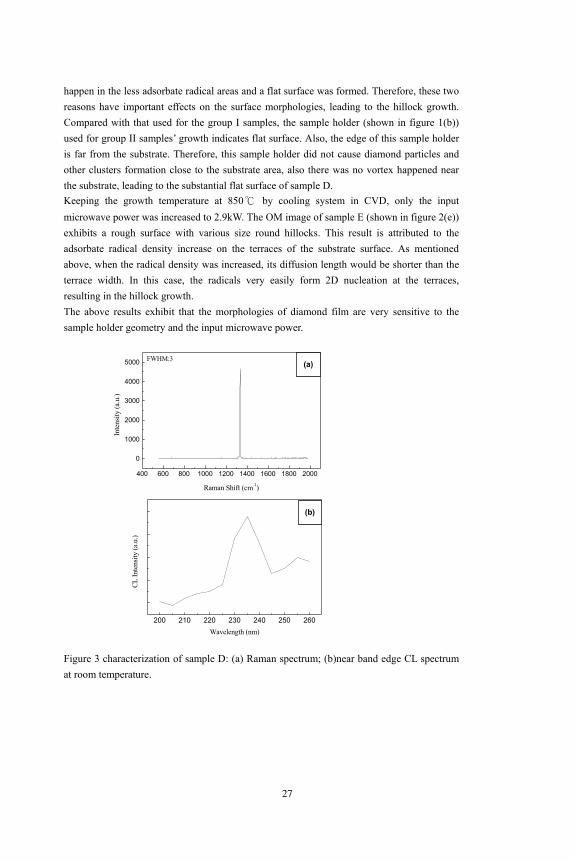
happen in the less adsorbate radical areas and a flat surface was formed. Therefore, these two reasons have important effects on the surface morphologies, leading to the hillock growth. Compared with that used for the group I samples, the sample holder (shown in figure 1(b)) used for group II samples’ growth indicates flat surface. Also, the edge of this sample holder is far from the substrate. Therefore, this sample holder did not cause diamond particles and other clusters formation close to the substrate area, also there was no vortex happened near the substrate, leading to the substantial flat surface of sample D. Keeping the growth temperature at 850 by cooling system in CVD, only the input microwave power was increased to 2.9kW. The OM image of sample E (shown in figure 2(e)) exhibits a rough surface with various size round hillocks. This result is attributed to the adsorbate radical density increase on the terraces of the substrate surface. As mentioned above, when the radical density was increased, its diffusion length would be shorter than the terrace width. In this case, the radicals very easily form 2D nucleation at the terraces, resulting in the hillock growth. The above results exhibit that the morphologies of diamond film are very sensitive to the sample holder geometry and the input microwave power. Figure 3 characterization of sample D: (a) Raman spectrum; (b)near band edge CL spectrum at room temperature.
400 600 800 1000 1200 1400 1600 1800 2000
0
1000
2000
3000
4000
5000 FWHM:3
Inte
nsity
(a.u
.)
Raman Shift (cm-1)
200 210 220 230 240 250 260
CL In
tens
ity (a
.u.)
Wavelength (nm)
(a)
(b)
28
(3) Characterization of diamond film of Sample D Figure 3(a) shows the Raman spectrum of as grown diamond film of Sample D. High-resolution Raman measurements on the same film shows that its peak position at 1332.61 cm-
1 with FWHM of 3cm-1. This peak width is narrow, indicating an accepted high quality, single crystal diamond film. In order to investigate the crystal quality of diamond film of Sample D, a cathodoluminescence (CL) emission measurement was carried out at room temperature. As shown in figure 3(b), the peak at 235 nm can be clearly observed. Considering that the CVD chamber was evacuated by only rotary pump system, there would be a lot of residual nitrogen in the chamber. Also, there are a lot of defects in the surface of Ib substrates. Therefore, it could be easily understood that our sample indicates a little wider Raman FWHM and a little weak free-exciton emission peak. We will further improve our growth condition and report the results in the future work. Conclusion A growth of homoepitaxial single crystal diamond film has been carried out by using a MPCVD of Seki AX6500X system with two different sample holders. Our results illustrate that diamond films are very sensitive to the growth parameter such as growth temperature and the input microwave power. Also, the results exhibit that the morphologies of diamond film are very sensitive to the sample holder geometry. Finally, the characterization of our sample reveals an accepted high quality single crystal film. References 1. C. S. Yan, Y. K. Vohra, H. M. Mao, and R. J. Hemley, Appl. Phys. Sci. 99, 12523(2002). 2. Y. Mokuno, A. Chayahara, Y. Soda, H. Yamada, Y. Horino, and N. Fujimori, Diamond
Relat. Mater. 15, 455(2006). 3. Y. Mokuno, A. Chayahara, and H. Yamada, Diamond Relat. Mater. 17(2008)415. 4. H. Okushi, H. Watanabe, S. Ri, S. Yamanaka, and T. Takeuchi, J. Cryst. Growth 237,
1269(2002). 5. T. Makino, N. Tokuda, H. Kata, M. Ogura, H. Watanabe, S. G. Ri, S. Yamasaki, and H.
Okushi, Jpn. J. Appl. Phys. 45, 1042(2006). 6. T. Teraji and T. Ito, J. Cryst. Growth 271, 409(2004). 7. J. Achard, F. Silva, A. Tallaire, X. Bonnin, G. Lombardi, K. Hassouni, and A. Gicquel, J.
Phys. D: Appl. Phys. 40, 6175(2007).

29
8. A. Tallaire, J. Achard, F. Silva, R. S. Sussmann, A. Gicquel. Diamond Relat. Mater. 14, 249(2005).
9. T. Teraji, S. Mitani, and T. Ito, Phys. Stat. Sol.(a) No.2, 395(2003). 10. C. L. Wang, M. Irie, and T. Ito, Diamond Relat. Mater. 9, 1650(2000). 11. C. L. Wang, M. Irie, and T. Ito, Jpn. J. Appl. Phys. 40, L212(2001). 12. N. Lee, A. Badzian, Diamond Relat. Mater. 6, 130(1997). 13. H. Yamada, A. Chayahara, Y. Mokuno, Y. Horino, S. Shikata, Diamond Relat. Mater. 15,
1738(2006).