Embed Size (px)
Citation preview

Toward Yield ExcellenceToward Yield ExcellenceToward Yield ExcellenceToward Yield Excellence
Page 1
漢民微測漢民微測漢民微測漢民微測漢民微測漢民微測漢民微測漢民微測
HMIHMI IntroductionIntroduction
Toward Yield ExcellenceToward Yield ExcellenceToward Yield ExcellenceToward Yield Excellence
Page 2
漢民微測漢民微測漢民微測漢民微測漢民微測漢民微測漢民微測漢民微測
�� Company ProfileCompany Profile
�� Product PortfolioProduct Portfolio
�� Core TechnologyCore Technology
�� R&D StrengthR&D Strength
�� HMI PerformanceHMI Performance
�� Motivation of EBI MarketMotivation of EBI Market
OutlinesOutlines
Toward Yield ExcellenceToward Yield ExcellenceToward Yield ExcellenceToward Yield Excellence
Page 3
漢民微測漢民微測漢民微測漢民微測漢民微測漢民微測漢民微測漢民微測
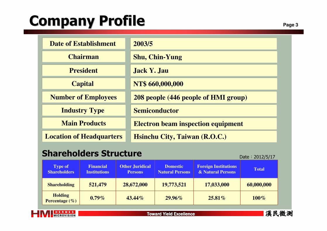
Chairman
2003/5
Industry Type
Main Products
Location of Headquarters
President
Capital
Number of Employees
Date of Establishment
Shu, Chin-Yung
Jack Y. Jau
NT$ 660,000,000
208 people (446 people of HMI group)
Semiconductor
Electron beam inspection equipment
Hsinchu City, Taiwan (R.O.C.)
Company ProfileCompany Profile
Type of
Shareholders
Financial
Institutions
Other Juridical
Persons
Domestic
Natural Persons
Foreign Institutions
& Natural PersonsTotal
Shareholding 521,479 28,672,000 19,773,521 17,033,000 60,000,000
Holding Percentage (%)
0.79% 43.44% 29.96% 25.81% 100%
Shareholders StructureShareholders Structure Date:2012/5/17
Toward Yield ExcellenceToward Yield ExcellenceToward Yield ExcellenceToward Yield Excellence
Page 4
漢民微測漢民微測漢民微測漢民微測漢民微測漢民微測漢民微測漢民微測
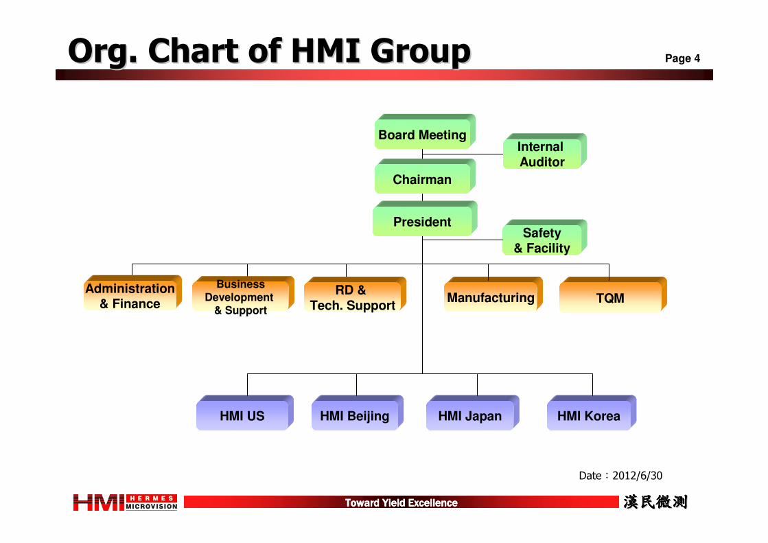
Org. Chart of HMI GroupOrg. Chart of HMI Group
HMI US HMI Beijing
Administration& Finance
Chairman
President
Board MeetingInternal Auditor
Safety& Facility
Date:2012/6/30
HMI Japan
Manufacturing
HMI Korea
TQMBusiness
Development & Support
RD & Tech. Support
Toward Yield ExcellenceToward Yield ExcellenceToward Yield ExcellenceToward Yield Excellence
Page 5
漢民微測漢民微測漢民微測漢民微測漢民微測漢民微測漢民微測漢民微測
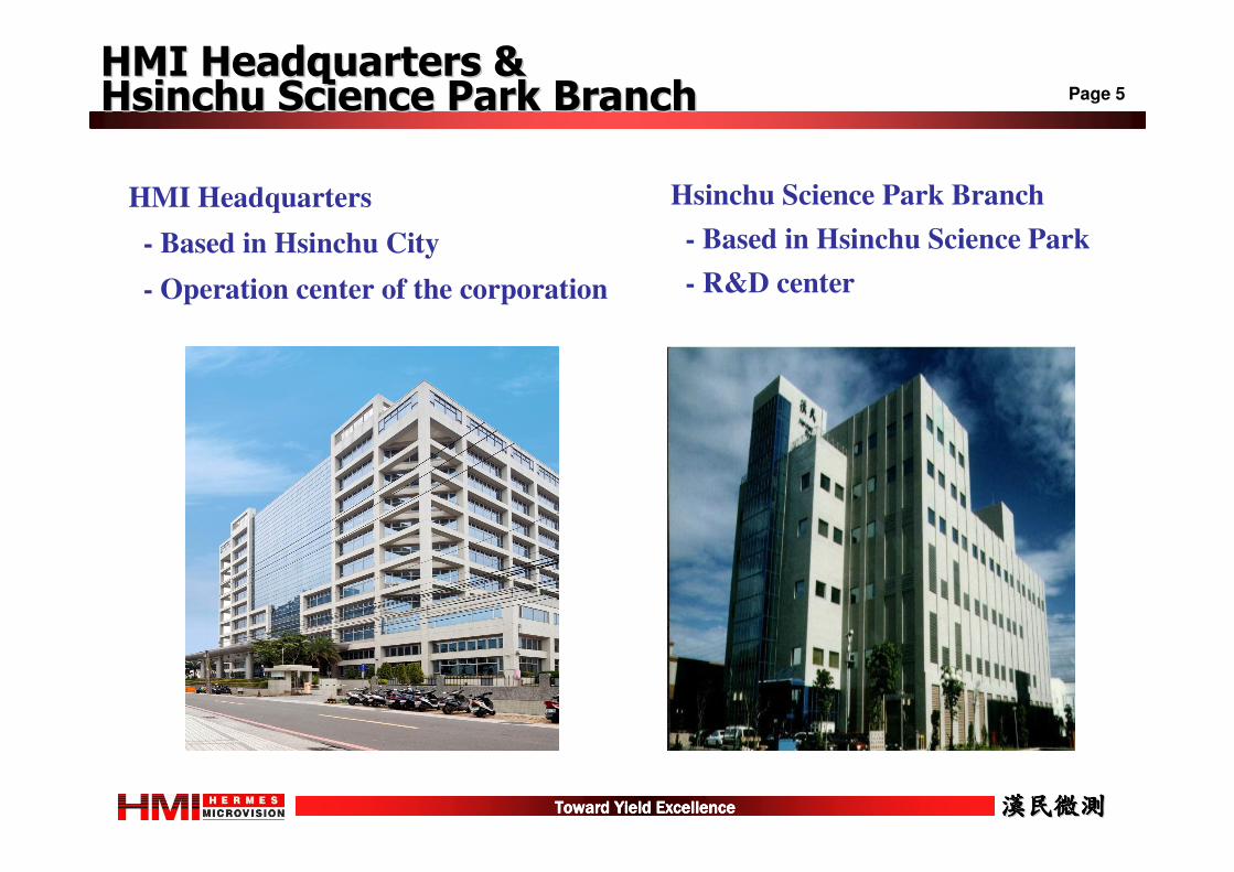
HMI Headquarters
- Based in Hsinchu City
- Operation center of the corporation
HMI Headquarters & HMI Headquarters & HsinchuHsinchu Science Park Branch Science Park Branch
Hsinchu Science Park Branch
- Based in Hsinchu Science Park
- R&D center
Toward Yield ExcellenceToward Yield ExcellenceToward Yield ExcellenceToward Yield Excellence
Page 6
漢民微測漢民微測漢民微測漢民微測漢民微測漢民微測漢民微測漢民微測
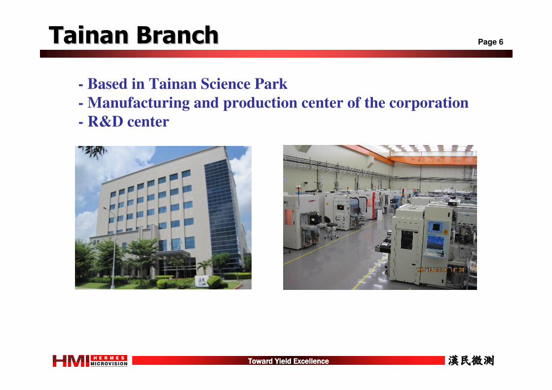
- Based in Tainan Science Park
- Manufacturing and production center of the corporation
- R&D center
Tainan BranchTainan Branch
Toward Yield ExcellenceToward Yield ExcellenceToward Yield ExcellenceToward Yield Excellence
Page 7
漢民微測漢民微測漢民微測漢民微測漢民微測漢民微測漢民微測漢民微測
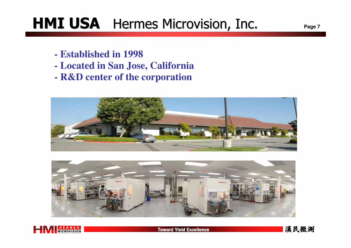
HMI USA HMI USA Hermes Hermes MicrovisionMicrovision, Inc., Inc.
- Established in 1998- Located in San Jose, California - R&D center of the corporation
Toward Yield ExcellenceToward Yield ExcellenceToward Yield ExcellenceToward Yield Excellence
Page 8
漢民微測漢民微測漢民微測漢民微測漢民微測漢民微測漢民微測漢民微測
HMI China, HMI Japan and HMI KoreaHMI China, HMI Japan and HMI Korea
HMI China: HMI China: Hermes Microvision Co., Ltd.(Beijing)- Located in Beijing
- Research and manufacture center of modules
HMI Japan: HMI Japan: Hermes Microvision Japan Inc. - Located in Tokyo
- Sales and technical service center
HMI Korea: HMI Korea: Hermes Microvision Korea Inc.- Located in Kyungki-do
- Sales and technical service center
Toward Yield ExcellenceToward Yield ExcellenceToward Yield ExcellenceToward Yield Excellence
Page 9
漢民微測漢民微測漢民微測漢民微測漢民微測漢民微測漢民微測漢民微測
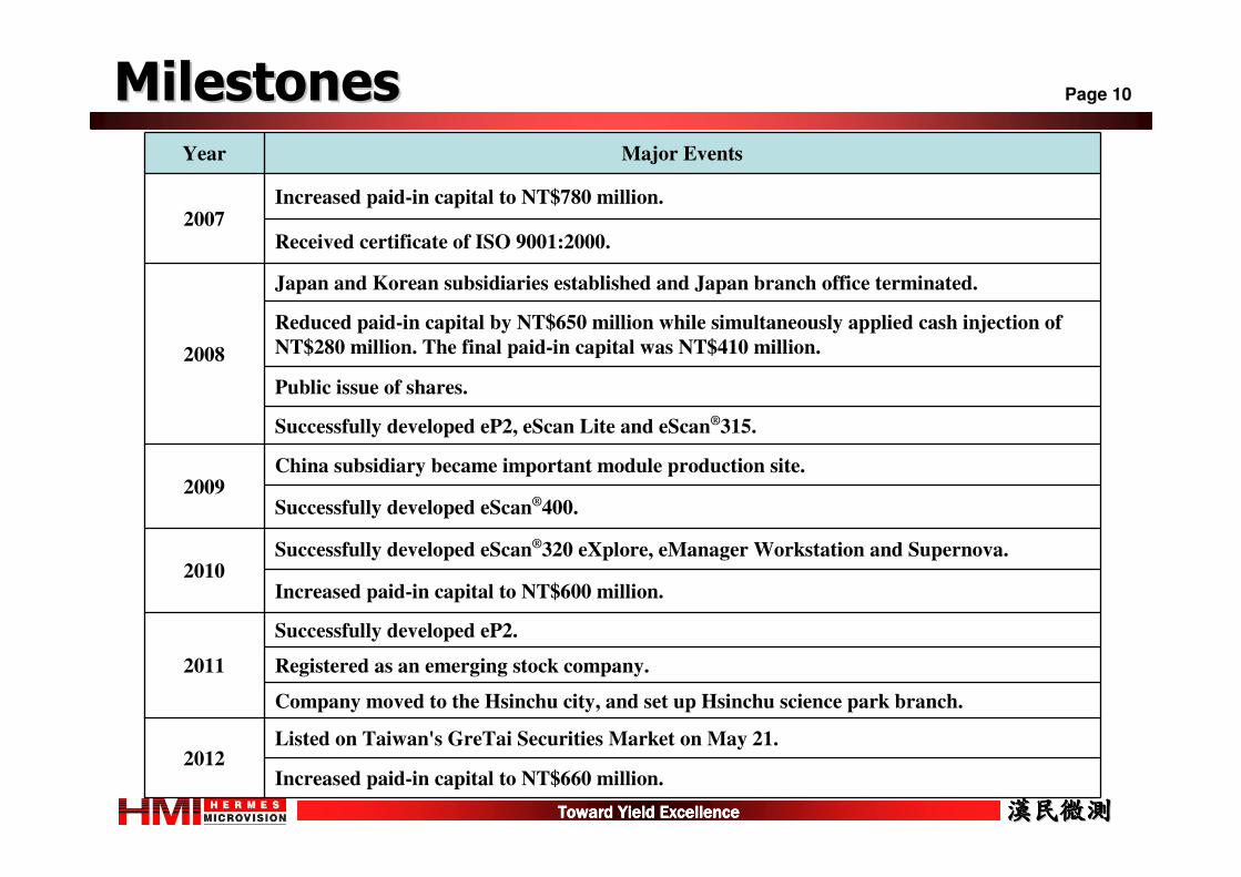
Year Major Events
1998Hermes Microvision, Inc. was founded in Silicon Valley, and started to be devoted to R & D for electron beam (e-beam) wafer inspection equipment.
2003
Hermes Microvision Precision Technology Co., Ltd. was founded in Hsinchu City, and the
paid-in capital is NT$1 million.
Company changed its name to Hermes Microvision, Inc..
Successfully developed eScan®300, the first inspection system of HMI.
2004
HMI Taiwan acquired 100% shares of HMI USA.
Company moved to the Hsinchu Science Park.
Sold first inspection system (eScan 300), and successfully penetrated the e-beam wafer inspection market that was monopolized by American and Japanese companies.
Set up Tainan branch at the Southern Taiwan Science Park to enlarge production scale.
Increased paid-in capital to NT$500 million.
2005Official gained entrance into the production line of Japanese and Korean semiconductor
foundries.
2006
Japan branch office established.
Successfully developed eScan®310 and eScan®380.
Received "2006 Supplier Excellence Awards in E-Beam Inspection" from Taiwan Semiconductor Manufacturing Company.
MilestonesMilestones
Toward Yield ExcellenceToward Yield ExcellenceToward Yield ExcellenceToward Yield Excellence
Page 10
漢民微測漢民微測漢民微測漢民微測漢民微測漢民微測漢民微測漢民微測
Listed on Taiwan's GreTai Securities Market on May 21. 2012
Increased paid-in capital to NT$660 million.
Year Major Events
2007Increased paid-in capital to NT$780 million.
Received certificate of ISO 9001:2000.
2008
Japan and Korean subsidiaries established and Japan branch office terminated.
Reduced paid-in capital by NT$650 million while simultaneously applied cash injection of
NT$280 million. The final paid-in capital was NT$410 million.
Public issue of shares.
Successfully developed eP2, eScan Lite and eScan®315.
2009China subsidiary became important module production site.
Successfully developed eScan®400.
2010Successfully developed eScan®320 eXplore, eManager Workstation and Supernova.
Increased paid-in capital to NT$600 million.
2011
Successfully developed eP2.
Registered as an emerging stock company.
Company moved to the Hsinchu city, and set up Hsinchu science park branch.
MilestonesMilestones

Toward Yield ExcellenceToward Yield ExcellenceToward Yield ExcellenceToward Yield Excellence
Page 11
漢民微測漢民微測漢民微測漢民微測漢民微測漢民微測漢民微測漢民微測
Product PortfolioProduct Portfolio
Toward Yield ExcellenceToward Yield ExcellenceToward Yield ExcellenceToward Yield Excellence
Page 12
漢民微測漢民微測漢民微測漢民微測漢民微測漢民微測漢民微測漢民微測
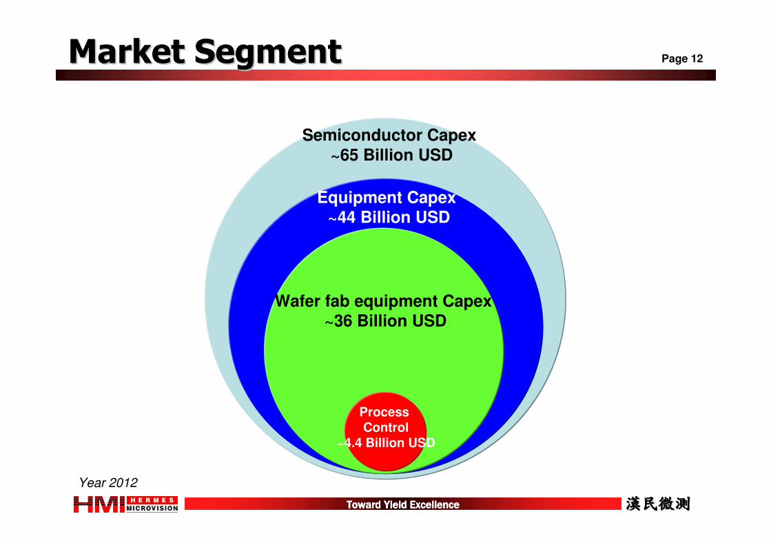
Semiconductor Capex
~65 Billion USD
Equipment Capex~44 Billion USD
Wafer fab equipment Capex~36 Billion USD
Process Control
~4.4 Billion USD
Market SegmentMarket Segment
Year 2012
Toward Yield ExcellenceToward Yield ExcellenceToward Yield ExcellenceToward Yield Excellence
Page 13
漢民微測漢民微測漢民微測漢民微測漢民微測漢民微測漢民微測漢民微測
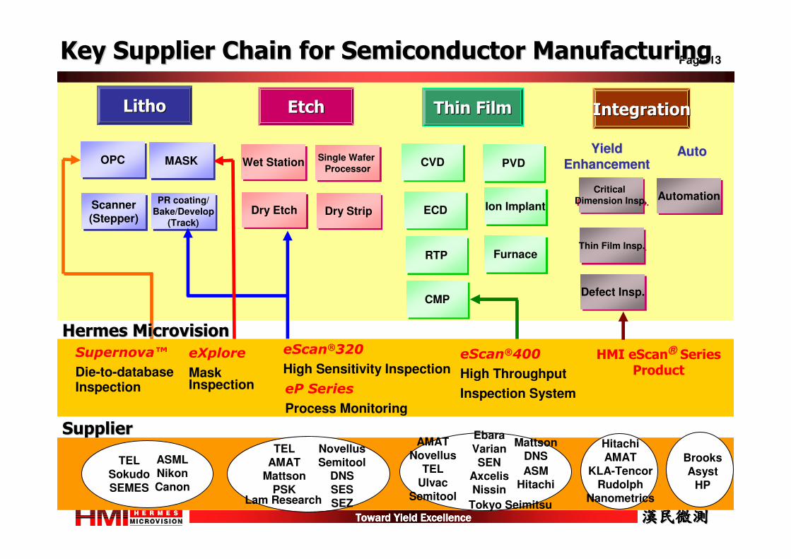
Thin FilmThin Film
CVDCVD PVDPVD
ECDECD
CMPCMP
Ion ImplantIon Implant
RTPRTP FurnaceFurnace
IntegrationIntegrationEtchEtchLithoLitho
OPCOPC Wet StationWet Station
Critical
Dimension Insp.
Critical
Dimension Insp.
MASKMASK
PR coating/
Bake/Develop
(Track)
PR coating/
Bake/Develop
(Track)
Scanner(Stepper)
Scanner(Stepper)
Single Wafer
Processor
Single Wafer
Processor
Dry EtchDry Etch Dry StripDry Strip
Thin Film Insp.Thin Film Insp.
Defect Insp.Defect Insp.
AutomationAutomation
Yield Yield
EnhancementEnhancementAutoAuto
SupplierSupplier
TEL
Sokudo
SEMES
ASMLNikon
Canon
Brooks
Asyst
HP
Lam Research
TEL
AMATMattson
PSK
Novellus
SemitoolDNS
SES
SEZ
Ebara
Varian
SENAxcelis
Nissin
AMAT
Novellus
TEL
Ulvac
Semitool
Hitachi
AMAT
KLA-TencorRudolph
Nanometrics
MattsonDNS
ASMHitachi
Tokyo Seimitsu
Key Supplier Chain for Semiconductor ManufacturingKey Supplier Chain for Semiconductor Manufacturing
eP Series
Process Monitoring
eXplore
Mask Inspection
eScan®320
High Sensitivity InspectioneScan®400
High Throughput
Inspection System
HMI eScan® Series Product
Hermes Hermes MicrovisionMicrovisionSupernova™
Die-to-databaseInspection
Toward Yield ExcellenceToward Yield ExcellenceToward Yield ExcellenceToward Yield Excellence
Page 14
漢民微測漢民微測漢民微測漢民微測漢民微測漢民微測漢民微測漢民微測
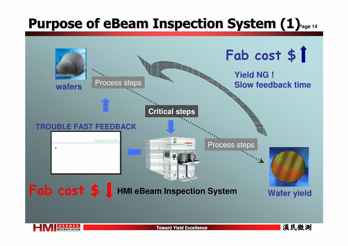
Process steps
Wafer yield
Critical steps
HMI eBeam Inspection System
TROUBLE FAST FEEDBACK
Process steps
Fab cost $
Yield NG !Slow feedback time
Purpose of Purpose of eBeameBeam Inspection System (1)Inspection System (1)
wafers
Fab cost $
Toward Yield ExcellenceToward Yield ExcellenceToward Yield ExcellenceToward Yield Excellence
Page 15
漢民微測漢民微測漢民微測漢民微測漢民微測漢民微測漢民微測漢民微測
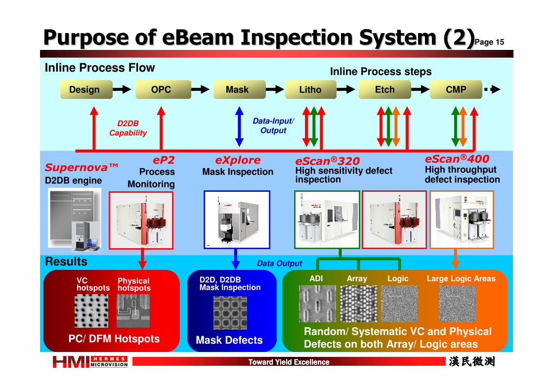
Inline Process Flow
PC/ DFM Hotspots
eP2Process
Monitoring
Design OPC Litho Etch CMPMask
eXplore Mask Inspection
Mask Defects
eScan®320 High sensitivity defect inspection
eScan®400 High throughput defect inspection
Data-Input/ Output
Data Output
Inline Process steps
Random/ Systematic VC and Physical
Defects on both Array/ Logic areas
ADI Large Logic AreasArray LogicVC hotspots
Physical hotspots
Results
D2D, D2DB Mask Inspection
D2DB Capability
Supernova™D2DB engine
Purpose of Purpose of eBeameBeam Inspection System (2)Inspection System (2)
Toward Yield ExcellenceToward Yield ExcellenceToward Yield ExcellenceToward Yield Excellence
Page 16
漢民微測漢民微測漢民微測漢民微測漢民微測漢民微測漢民微測漢民微測
Core Technology Core Technology
Toward Yield ExcellenceToward Yield ExcellenceToward Yield ExcellenceToward Yield Excellence
Page 17
漢民微測漢民微測漢民微測漢民微測漢民微測漢民微測漢民微測漢民微測
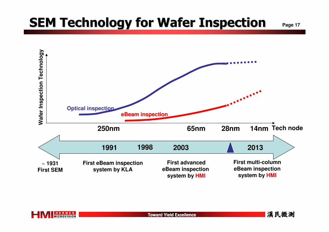
1991 2003 2013
65nm 14nm250nm
~ 1931First SEM
First eBeam inspectionsystem by KLA
First advancedeBeam inspection
system by HMI
First multi-columneBeam inspection
system by HMI
SEM Technology for Wafer InspectionSEM Technology for Wafer Inspection
eBeameBeam inspectioninspection
Wafe
r In
sp
ecti
on
Tech
no
log
y
Optical inspection
1998
Tech node28nm
Toward Yield ExcellenceToward Yield ExcellenceToward Yield ExcellenceToward Yield Excellence
Page 18
漢民微測漢民微測漢民微測漢民微測漢民微測漢民微測漢民微測漢民微測
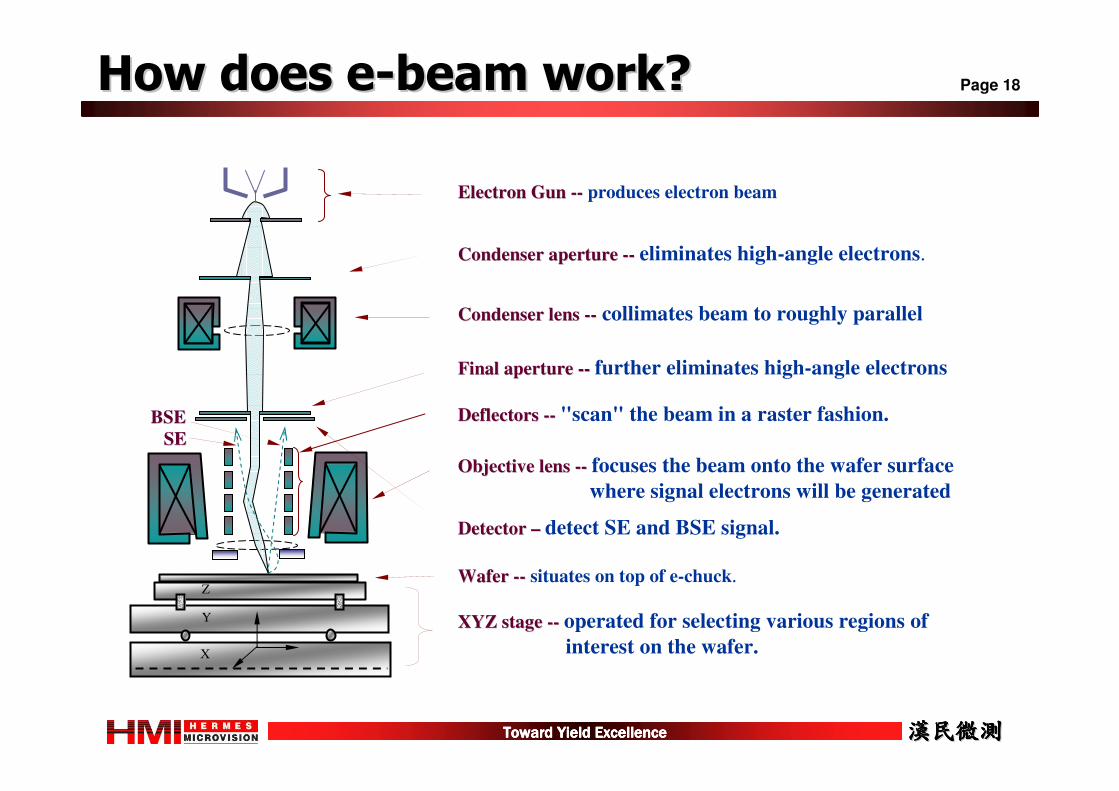
Objective lens Objective lens ---- focuses the beam onto the wafer surface
where signal electrons will be generated
X
Y
Z
XYZ stage XYZ stage ---- operated for selecting various regions of
interest on the wafer.
Deflectors Deflectors ---- "scan" the beam in a raster fashion.
Final aperture Final aperture ---- further eliminates high-angle electrons
Condenser lens Condenser lens ---- collimates beam to roughly parallel
Condenser aperture Condenser aperture ---- eliminates high-angle electrons.
Electron Gun Electron Gun ---- produces electron beam
SESEBSEBSE
Wafer Wafer ---- situates on top of e-chuck.
Detector Detector –– detect SE and BSE signal.
How does eHow does e--beam work?beam work?
Toward Yield ExcellenceToward Yield ExcellenceToward Yield ExcellenceToward Yield Excellence
Page 19
漢民微測漢民微測漢民微測漢民微測漢民微測漢民微測漢民微測漢民微測
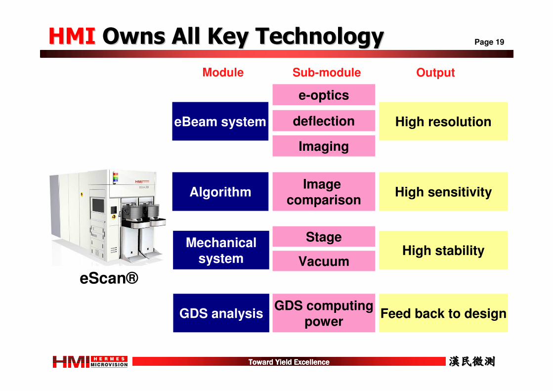
eBeam system
Algorithm
Mechanicalsystem
GDS analysis
e-optics
Image comparison
Stage
GDS computingpower
deflection
Imaging
Vacuum
High resolution
High sensitivity
High stability
Feed back to design
Module Sub-module Output
eScan®
HMIHMI Owns All Key TechnologyOwns All Key Technology
Toward Yield ExcellenceToward Yield ExcellenceToward Yield ExcellenceToward Yield Excellence
Page 20
漢民微測漢民微測漢民微測漢民微測漢民微測漢民微測漢民微測漢民微測
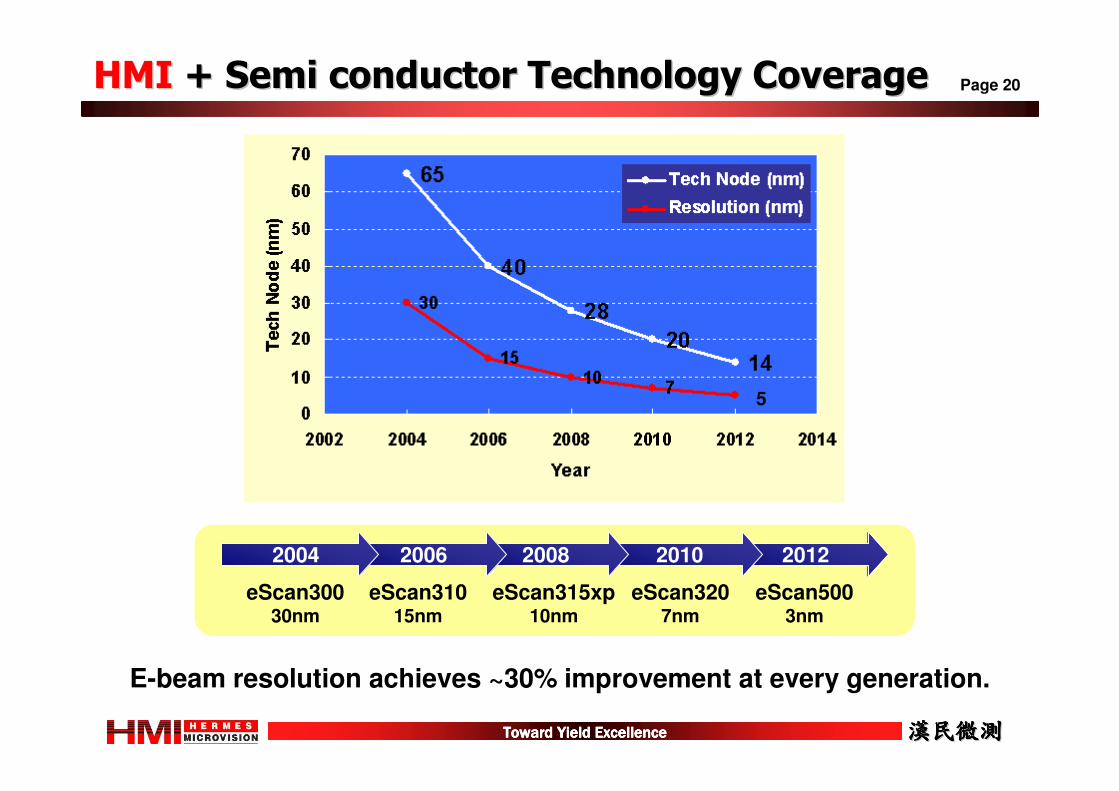
2012201020082006
eScan30030nm
eScan31015nm
eScan315xp10nm
eScan3207nm
eScan5003nm
2004
E-beam resolution achieves ~30% improvement at every generation.
5
HMIHMI + Semi conductor Technology Coverage+ Semi conductor Technology Coverage
Toward Yield ExcellenceToward Yield ExcellenceToward Yield ExcellenceToward Yield Excellence
Page 21
漢民微測漢民微測漢民微測漢民微測漢民微測漢民微測漢民微測漢民微測
R&D StrengthR&D Strength
Toward Yield ExcellenceToward Yield ExcellenceToward Yield ExcellenceToward Yield Excellence
Page 22
漢民微測漢民微測漢民微測漢民微測漢民微測漢民微測漢民微測漢民微測
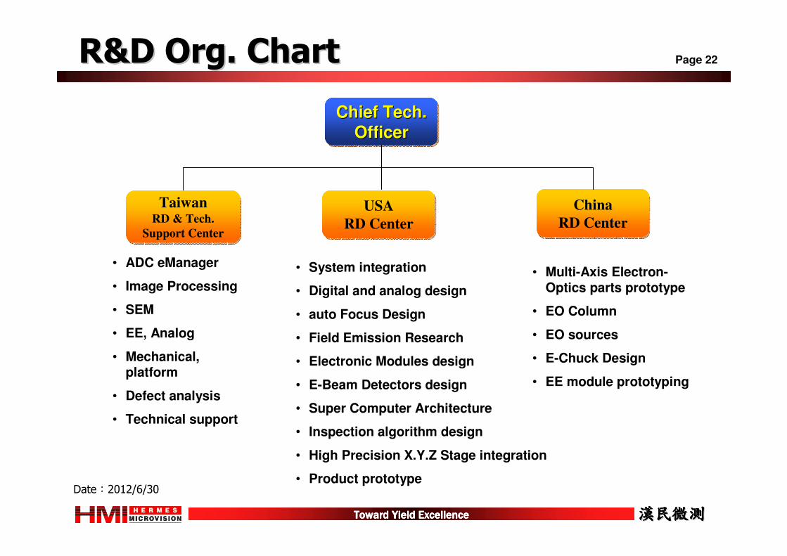
R&D Org. ChartR&D Org. Chart
TaiwanRD & Tech.
Support Center
TaiwanRD & Tech.
Support Center
USA
RD Center
USA
RD CenterChina
RD Center
China
RD Center
Chief Tech. Officer
Chief Tech. Chief Tech.
OfficerOfficer
• ADC eManager
• Image Processing
• SEM
• EE, Analog
• Mechanical, platform
• Defect analysis
• Technical support
• System integration
• Digital and analog design
• auto Focus Design
• Field Emission Research
• Electronic Modules design
• E-Beam Detectors design
• Super Computer Architecture
• Inspection algorithm design
• High Precision X.Y.Z Stage integration
• Product prototype
• Multi-Axis Electron-Optics parts prototype
• EO Column
• EO sources
• E-Chuck Design
• EE module prototyping
Date:2012/6/30
Toward Yield ExcellenceToward Yield ExcellenceToward Yield ExcellenceToward Yield Excellence
Page 23
漢民微測漢民微測漢民微測漢民微測漢民微測漢民微測漢民微測漢民微測
HMI PerformanceHMI Performance
Toward Yield ExcellenceToward Yield ExcellenceToward Yield ExcellenceToward Yield Excellence
Page 24
漢民微測漢民微測漢民微測漢民微測漢民微測漢民微測漢民微測漢民微測
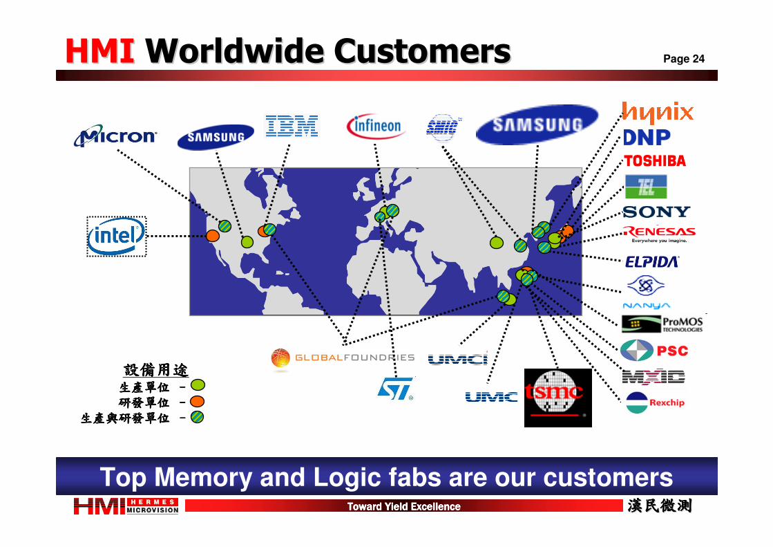
設備用途設備用途設備用途設備用途生產單位生產單位生產單位生產單位 ––––
研發單位研發單位研發單位研發單位 ––––
生產與研發單位生產與研發單位生產與研發單位生產與研發單位 ––––
HMIHMI Worldwide CustomersWorldwide Customers
Top Memory and Logic fabs are our customers
Toward Yield ExcellenceToward Yield ExcellenceToward Yield ExcellenceToward Yield Excellence
Page 25
漢民微測漢民微測漢民微測漢民微測漢民微測漢民微測漢民微測漢民微測
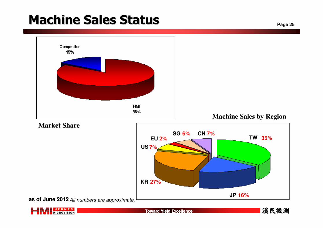
Machine Sales StatusMachine Sales Status
Machine Sales by Region
as of June 2012as of June 2012
Market ShareMarket Share
EU 2%SG 6% CN 7%
KR 27%
JP 16%
TW 35%
US 7%
All numbers are approximate.
Toward Yield ExcellenceToward Yield ExcellenceToward Yield ExcellenceToward Yield Excellence
Page 26
漢民微測漢民微測漢民微測漢民微測漢民微測漢民微測漢民微測漢民微測
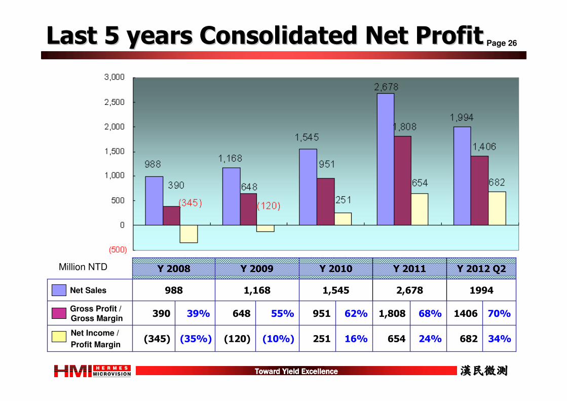
Last 5 years Consolidated Net ProfitLast 5 years Consolidated Net Profit
24%
68%
654
1,808
2,678
Y 2011
34%
70%
16%
62%
(10%)
55%
(35%)
39% 1406951648390Gross Profit / Gross Margin
Net Income /
Profit Margin
Net Sales
682251(120)(345)
19941,5451,168988
Y 2012 Q2Y 2010Y 2009Y 2008Million NTD
Toward Yield ExcellenceToward Yield ExcellenceToward Yield ExcellenceToward Yield Excellence
Page 27
漢民微測漢民微測漢民微測漢民微測漢民微測漢民微測漢民微測漢民微測
Motivation of EBI MarketMotivation of EBI Market
Toward Yield ExcellenceToward Yield ExcellenceToward Yield ExcellenceToward Yield Excellence
Page 28
漢民微測漢民微測漢民微測漢民微測漢民微測漢民微測漢民微測漢民微測
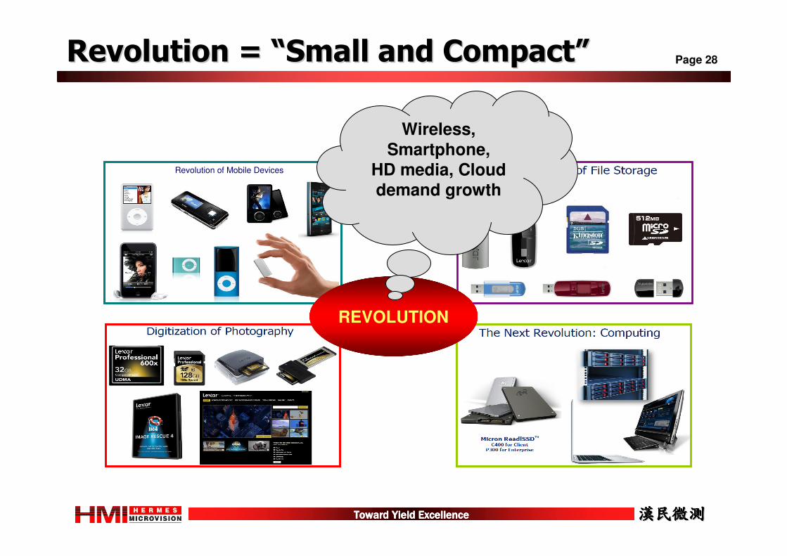
REVOLUTION
Revolution of Mobile Devices
Wireless,
Smartphone, HD media, Cloud demand growth
Revolution = Revolution = ““Small and CompactSmall and Compact””
Toward Yield ExcellenceToward Yield ExcellenceToward Yield ExcellenceToward Yield Excellence
Page 29
漢民微測漢民微測漢民微測漢民微測漢民微測漢民微測漢民微測漢民微測
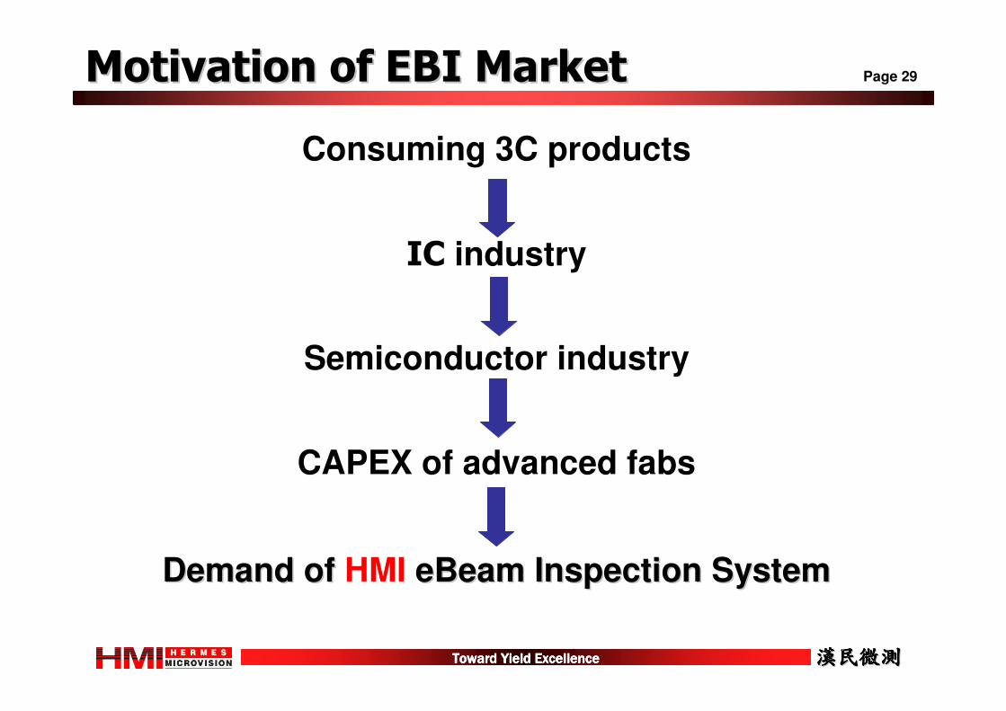
Motivation of EBI MarketMotivation of EBI Market
Consuming 3C products
IC industry
Semiconductor industry
CAPEX of advanced fabs
Demand of Demand of HMI eBeameBeam Inspection SystemInspection System
Toward Yield ExcellenceToward Yield ExcellenceToward Yield ExcellenceToward Yield Excellence
Page 30
漢民微測漢民微測漢民微測漢民微測漢民微測漢民微測漢民微測漢民微測
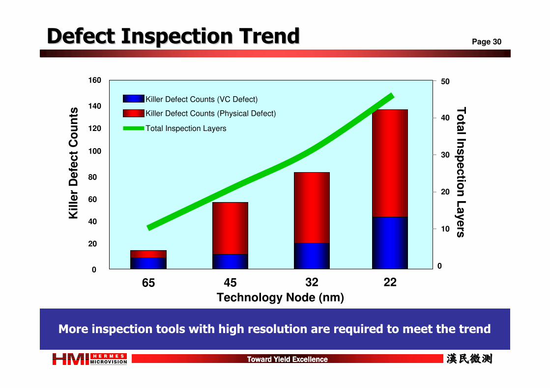
More inspection tools with high resolution are required to meet the trend
To
tal In
sp
ectio
n L
ayers
0
10
20
30
40
50K
ille
r D
efe
ct
Co
un
ts
0
20
40
60
80
100
120
140
160
Killer Defect Counts (Physical Defect)
Killer Defect Counts (VC Defect)
Total Inspection Layers
65 45 32 22
Technology Node (nm)
Defect Inspection TrendDefect Inspection Trend