Embed Size (px)
Citation preview

FN3676 Rev.6.00 Page 1 of 15Feb 12, 2020
FN3676Rev.6.00
Feb 12, 2020
HIP408280V, 1.25A Peak Current H-Bridge FET Driver
DATASHEET
The HIP4082 is a medium frequency, medium voltage H-Bridge N-Channel MOSFET driver IC, available in 16 lead plastic SOIC (N) and DIP packages.
Specifically targeted for PWM motor control and UPS applications, bridge based designs are made simple and flexible with the HIP4082 H-bridge driver. With operation up to 80V, the device is best suited to applications of moderate power levels.
Similar to the HIP4081, it has a flexible input protocol for driving every possible switch combination except those which would cause a shoot-through condition. The HIP4082’s reduced drive current allows smaller packaging and it has a much wider range of programmable dead times (0.1 to 4.5s) making it ideal for switching frequencies up to 200kHz. The HIP4082 does not contain an internal charge pump, but does incorporate non-latching level-shift translation control of the upper drive circuits.
This set of features and specifications is optimized for applications where size and cost are important. For applications needing higher drive capability the HIP4080A and HIP4081A are recommended.
Features
• Independently Drives 4 N-Channel FET in Half Bridge or Full Bridge Configurations
• Bootstrap Supply Max Voltage to 95VDC
• Drives 1000pF Load in Free Air at 50°C with Rise and Fall Times of Typically 15ns
• User-Programmable Dead Time (0.1 to 4.5s)
• DIS (Disable) Overrides Input Control and Refreshes Bootstrap Capacitor when Pulled Low
• Input Logic Thresholds Compatible with 5V to 15V Logic Levels
• Shoot-Through Protection
• Undervoltage Protection
• Pb-Free Plus Anneal Available (RoHS Compliant)
Applications
• UPS Systems
• DC Motor Controls
• Full Bridge Power Supplies
• Switching Power Amplifiers
• Noise Cancellation Systems
• Battery Powered Vehicles
• Peripherals
• Medium/Large Voice Coil Motors
• Related Literature
- TB363, Guidelines for Handling and Processing Moisture Sensitive Surface Mount Devices (SMDs)

HIP4082
PinoutHIP4082
(PDIP, SOIC)TOP VIEW
Ordering Information
PART NUMBER PART MARKINGTEMP.
RANGE (°C) PACKAGEPKG.
DWG. #
HIP4082IBZ* (Note) 4082IBZ -55 to +125 16 Ld SOIC (N) (Pb-free) M16.15
HIP4082IPZ (Note) HIP4082IPZ -55 to +125 16 Ld PDIP** (Pb-free) E16.3
*Add “T” suffix for tape and reel.
NOTE: Pb-free plus anneal products employ special Pb-free material sets; molding compounds/die attach materials and 100% matte tin plate termination finish, which are RoHS compliant and compatible with both SnPb and Pb-free soldering operations. Pb-free products are MSL classified at Pb-free peak reflow temperatures that meet or exceed the Pb-free requirements of IPC/JEDEC J STD-020.
**Pb-free PDIPs can be used for through hole wave solder processing only. They are not intended for use in Reflow solder processing applications.
14
15
16
9
13
12
11
10
1
2
3
4
5
7
6
8
BHB
BHI
BLI
ALI
DEL
VSS
DIS
AHI
BHO
BLO
ALO
VDD
AHS
AHO
AHB
BHS
FN3676 Rev.6.00 Page 2 of 15Feb 12, 2020

HIP4082
Application Block Diagram
Functional Block Diagram
80V
GND
LOAD
HIP4082
GND
12V
AHI
ALI
BLI
BHI BLO
BHS
BHO
ALO
AHS
AHO
3
8
2
7
4
12
5
6
TURN-ONDELAY
DRIVER
13
LEVELSHIFT
DRIVER
AHB
AHS
9
10
11
14
15
16
1
DRIVER
TURN-ONDELAY
DRIVER
TURN-ONDELAY
LEVELSHIFT
AHO
BHB
BHS
BHO
ALO BLO
TURN-ONDELAY
UNDERVOLTAGEDETECTOR
VDD
BHI
AHI
DIS
ALI
VDD
DEL
BLI
VSS
U/V U/V
FN3676 Rev.6.00 Page 3 of 15Feb 12, 2020
HIP4082
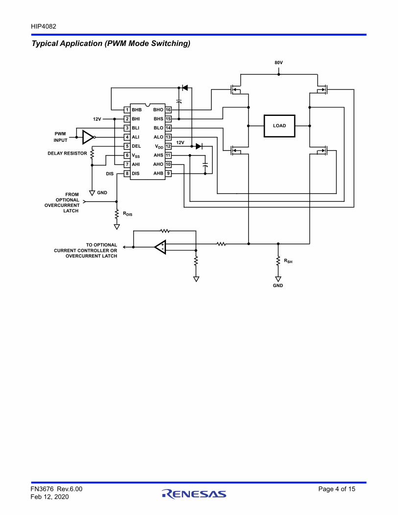
Typical Application (PWM Mode Switching)
80V
12V
12V
DIS
GND
GND
TO OPTIONALCURRENT CONTROLLER OR
PWM
LOAD
INPUT
+-
14
15
16
9
13
12
11
10
1
2
3
4
5
7
6
8
BHB
BHI
BLI
ALI
DEL
VSS
DIS
AHI
BHO
BLO
ALO
VDD
AHS
AHO
AHB
BHS
OVERCURRENT LATCH
RDIS
DELAY RESISTOR
FROMOPTIONAL
OVERCURRENT LATCH
RSH
FN3676 Rev.6.00 Page 4 of 15Feb 12, 2020
HIP4082
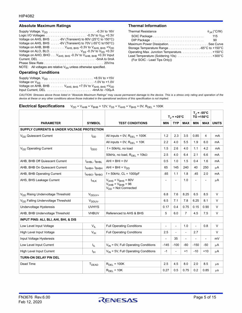
Absolute Maximum Ratings Thermal InformationSupply Voltage, VDD . . . . . . . . . . . . . . . . . . . . . . . . . . . -0.3V to 16VLogic I/O Voltages . . . . . . . . . . . . . . . . . . . . . . . -0.3V to VDD +0.3VVoltage on AHS, BHS . . . . . -6V (Transient) to 80V (25°C to 150°C)Voltage on AHS, BHS . . . . . -6V (Transient) to 70V (-55°C to150°C)Voltage on AHB, BHB . . . . . . . . VAHS, BHS -0.3V to VAHS, BHS +VDDVoltage on ALO, BLO. . . . . . . . . . . . . . . . . . VSS -0.3V to VDD +0.3VVoltage on AHO, BHO . . . VAHS, BHS -0.3V to VAHB, BHB +0.3V InputCurrent, DEL . . . . . . . . . . . . . . . . . . . . . . . . . . . . . . . . -5mA to 0mAPhase Slew Rate . . . . . . . . . . . . . . . . . . . . . . . . . . . . . . . . . . 20V/nsNOTE: All voltages are relative VSS unless otherwise specified.
Thermal Resistance JA (°C/W)
SOIC Package . . . . . . . . . . . . . . . . . . . . . . . . . . . . . 115DIP Package . . . . . . . . . . . . . . . . . . . . . . . . . . . . . . 90
Maximum Power Dissipation. . . . . . . . . . . . . . . . . . . . . . . . See CurveStorage Temperature Range . . . . . . . . . . . . . . . . . . -65°C to +150°COperating Max. Junction Temperature. . . . . . . . . . . . . . . . . . +150°CLead Temperature (Soldering 10s) . . . . . . . . . . . . . . . . . . . . +300°C
(For SOIC - Lead Tips Only))
Operating ConditionsSupply Voltage, VDD . . . . . . . . . . . . . . . . . . . . . . . . . +8.5V to +15VVoltage on VSS. . . . . . . . . . . . . . . . . . . . . . . . . . . . . . -1.0V to +1.0VVoltage on AHB, BHB . . . . . . . VAHS, BHS +7.5V to VAHS, BHS +VDDInput Current, DEL . . . . . . . . . . . . . . . . . . . . . . . . . -4mA to -100A
CAUTION: Stresses above those listed in “Absolute Maximum Ratings” may cause permanent damage to the device. This is a stress only rating and operation of thedevice at these or any other conditions above those indicated in the operational sections of this specification is not implied.
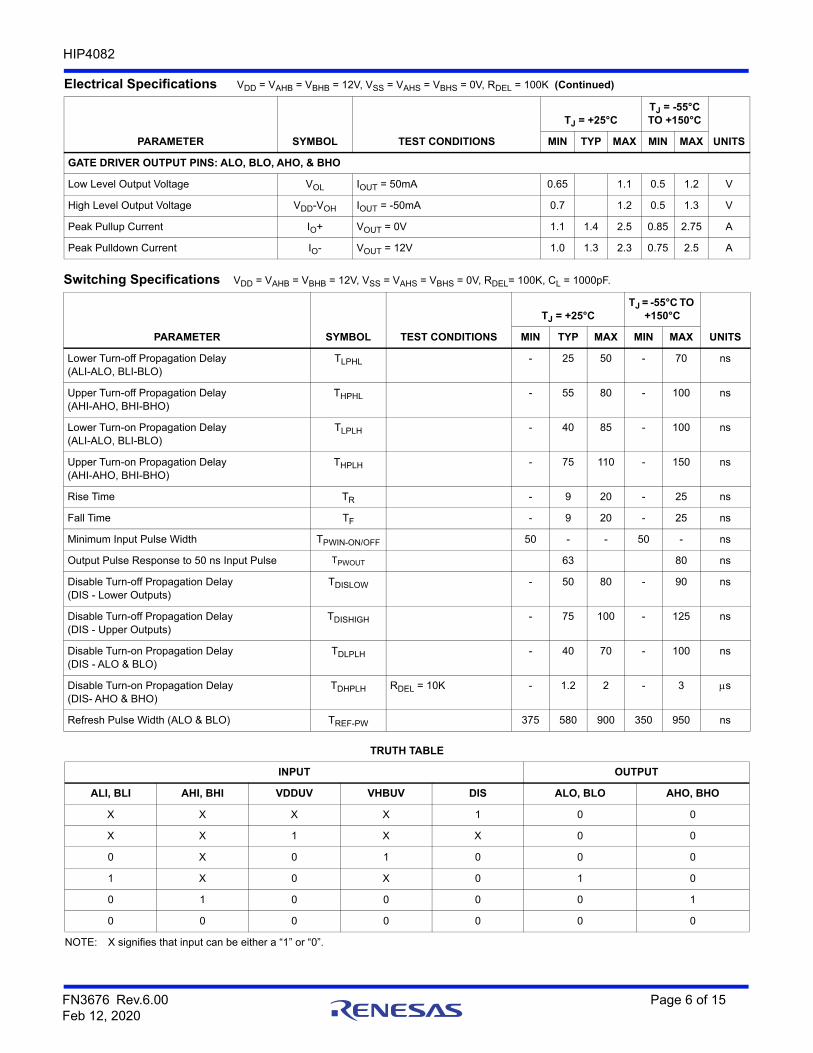
Electrical Specifications VDD = VAHB = VBHB = 12V, VSS = VAHS = VBHS = 0V, RDEL = 100K
PARAMETER SYMBOL TEST CONDITIONS
TJ = +25°CTJ = -55°C TO +150°C
UNITSMIN TYP MAX MIN MAX
SUPPLY CURRENTS & UNDER VOLTAGE PROTECTION
VDD Quiescent Current IDD All inputs = 0V, RDEL = 100K 1.2 2.3 3.5 0.85 4 mA
All inputs = 0V, RDEL = 10K 2.2 4.0 5.5 1.9 6.0 mA
VDD Operating Current IDDO f = 50kHz, no load 1.5 2.6 4.0 1.1 4.2 mA
50kHz, no load, RDEL = 10k 2.5 4.0 6.4 2.1 6.6 mA
AHB, BHB Off Quiescent Current IAHBL, IBHBL AHI = BHI = 0V 0.5 1.0 1.5 0.4 1.6 mA
AHB, BHB On Quiescent Current IAHBH, IBHBH AHI = BHI = VDD 65 145 240 40 250 A
AHB, BHB Operating Current IAHBO, IBHBO f = 50kHz, CL = 1000pF .65 1.1 1.8 .45 2.0 mA
AHS, BHS Leakage Current IHLK VAHS = VBHS = 80VVAHB = VBHB = 96VDD = Not Connected
- - 1.0 - - A
VDD Rising Undervoltage Threshold VDDUV+ 6.8 7.6 8.25 6.5 8.5 V
VDD Falling Undervoltage Threshold VDDUV- 6.5 7.1 7.8 6.25 8.1 V
Undervoltage Hysteresis UVHYS 0.17 0.4 0.75 0.15 0.90 V
AHB, BHB Undervoltage Threshold VHBUV Referenced to AHS & BHS 5 6.0 7 4.5 7.5 V
INPUT PINS: ALI, BLI, AHI, BHI, & DIS
Low Level Input Voltage VIL Full Operating Conditions - - 1.0 - 0.8 V
High Level Input Voltage VIH Full Operating Conditions 2.5 - - 2.7 V
Input Voltage Hysteresis - 35 - - - mV
Low Level Input Current IIL VIN = 0V, Full Operating Conditions -145 -100 -60 -150 -50 A
High Level Input Current IIH VIN = 5V, Full Operating Conditions -1 - +1 -10 +10 A
TURN-ON DELAY PIN DEL
Dead Time TDEAD RDEL = 100K 2.5 4.5 8.0 2.0 8.5 s
RDEL = 10K 0.27 0.5 0.75 0.2 0.85 s
FN3676 Rev.6.00 Page 5 of 15Feb 12, 2020
HIP4082
GATE DRIVER OUTPUT PINS: ALO, BLO, AHO, & BHO
Low Level Output Voltage VOL IOUT = 50mA 0.65 1.1 0.5 1.2 V
High Level Output Voltage VDD-VOH IOUT = -50mA 0.7 1.2 0.5 1.3 V
Peak Pullup Current IO+ VOUT = 0V 1.1 1.4 2.5 0.85 2.75 A
Peak Pulldown Current IO- VOUT = 12V 1.0 1.3 2.3 0.75 2.5 A
Switching Specifications VDD = VAHB = VBHB = 12V, VSS = VAHS = VBHS = 0V, RDEL= 100K, CL = 1000pF.
PARAMETER SYMBOL TEST CONDITIONS
TJ = +25°CTJ = -55°C TO
+150°C
UNITSMIN TYP MAX MIN MAX
Lower Turn-off Propagation Delay(ALI-ALO, BLI-BLO)
TLPHL - 25 50 - 70 ns
Upper Turn-off Propagation Delay(AHI-AHO, BHI-BHO)
THPHL - 55 80 - 100 ns
Lower Turn-on Propagation Delay(ALI-ALO, BLI-BLO)
TLPLH - 40 85 - 100 ns
Upper Turn-on Propagation Delay(AHI-AHO, BHI-BHO)
THPLH - 75 110 - 150 ns
Rise Time TR - 9 20 - 25 ns
Fall Time TF - 9 20 - 25 ns
Minimum Input Pulse Width TPWIN-ON/OFF 50 - - 50 - ns
Output Pulse Response to 50 ns Input Pulse TPWOUT 63 80 ns
Disable Turn-off Propagation Delay(DIS - Lower Outputs)
TDISLOW - 50 80 - 90 ns
Disable Turn-off Propagation Delay(DIS - Upper Outputs)
TDISHIGH - 75 100 - 125 ns
Disable Turn-on Propagation Delay(DIS - ALO & BLO)
TDLPLH - 40 70 - 100 ns
Disable Turn-on Propagation Delay (DIS- AHO & BHO)
TDHPLH RDEL = 10K - 1.2 2 - 3 s
Refresh Pulse Width (ALO & BLO) TREF-PW 375 580 900 350 950 ns
TRUTH TABLE
INPUT OUTPUT
ALI, BLI AHI, BHI VDDUV VHBUV DIS ALO, BLO AHO, BHO
X X X X 1 0 0
X X 1 X X 0 0
0 X 0 1 0 0 0
1 X 0 X 0 1 0
0 1 0 0 0 0 1
0 0 0 0 0 0 0
NOTE: X signifies that input can be either a “1” or “0”.
Electrical Specifications VDD = VAHB = VBHB = 12V, VSS = VAHS = VBHS = 0V, RDEL = 100K (Continued)
PARAMETER SYMBOL TEST CONDITIONS
TJ = +25°CTJ = -55°C TO +150°C
UNITSMIN TYP MAX MIN MAX
FN3676 Rev.6.00 Page 6 of 15Feb 12, 2020

HIP4082
FN3676 Rev.6.00 Page 7 of 15Feb 12, 2020
Pin Descriptions
PINNUMBER SYMBOL DESCRIPTION
1 BHB B High-side Bootstrap supply. External bootstrap diode and capacitor are required. Connect cathode of bootstrapdiode and positive side of bootstrap capacitor to this pin.
2 BHI B High-side Input. Logic level input that controls BHO driver (Pin 16). BLI (Pin 3) high level input overrides BHI highlevel input to prevent half-bridge shoot-through, see Truth Table. DIS (Pin 8) high level input overrides BHI high levelinput. The pin can be driven by signal levels of 0V to 15V (no greater than VDD).
3 BLI B Low-side Input. Logic level input that controls BLO driver (Pin 14). If BHI (Pin 2) is driven high or not connectedexternally then BLI controls both BLO and BHO drivers, with dead time set by delay currents at DEL (Pin 5). DIS (Pin8) high level input overrides BLI high level input. The pin can be driven by signal levels of 0V to 15V (no greater thanVDD).
4 ALI A Low-side Input. Logic level input that controls ALO driver (Pin 13). If AHI (Pin 7) is driven high or not connectedexternally then ALI controls both ALO and AHO drivers, with dead time set by delay currents at DEL (Pin 5). DIS (Pin8) high level input overrides ALI high level input. The pin can be driven by signal levels of 0V to 15V (no greater thanVDD).
5 DEL Turn-on DELay. Connect resistor from this pin to VSS to set timing current that defines the dead time between drivers.All drivers turn-off with no adjustable delay, so the DEL resistor guarantees no shoot-through by delaying the turn-onof all drivers. The voltage across the DEL resistor is approximately Vdd -2V.
6 VSS Chip negative supply, generally will be ground.
7 AHI A High-side Input. Logic level input that controls AHO driver (Pin 10). ALI (Pin 4) high level input overrides AHI highlevel input to prevent half-bridge shoot-through, see Truth Table. DIS (Pin 8) high level input overrides AHI high levelinput. The pin can be driven by signal levels of 0V to 15V (no greater than VDD).
8 DIS DISable input. Logic level input that when taken high sets all four outputs low. DIS high overrides all other inputs. WhenDIS is taken low the outputs are controlled by the other inputs. The pin can be driven by signal levels of 0V to 15V (nogreater than VDD).
9 AHB A High-side Bootstrap supply. External bootstrap diode and capacitor are required. Connect cathode of bootstrapdiode and positive side of bootstrap capacitor to this pin.
10 AHO A High-side Output. Connect to gate of A High-side power MOSFET.
11 AHS A High-side Source connection. Connect to source of A High-side power MOSFET. Connect negative side of bootstrapcapacitor to this pin.
12 VDD Positive supply to control logic and lower gate drivers. De-couple this pin to VSS (Pin 6).
13 ALO A Low-side Output. Connect to gate of A Low-side power MOSFET.
14 BLO B Low-side Output. Connect to gate of B Low-side power MOSFET.
15 BHS B High-side Source connection. Connect to source of B High-side power MOSFET. Connect negative side of bootstrapcapacitor to this pin.
16 BHO B High-side Output. Connect to gate of B High-side power MOSFET.

HIP4082
Timing Diagrams
FIGURE 1. INDEPENDENT MODE
FIGURE 2. BISTATE MODE
FIGURE 3. DISABLE FUNCTION
DIS=0
XLI
XHI
XLO
XHO
TLPHL THPHL
THPLH TLPLH TR(10% - 90%)
TF(10% - 90%)
X = A OR B, A AND B HALVES OF BRIDGE CONTROLLER ARE INDEPENDENT
and UV
DIS=0
XLI
XHI = HI OR NOT CONNECTED
XLO
XHO
and UV
DIS or UV
XLI
XHI
XLO
XHO
TDLPLH TDIS
TDHPLH
TREF-PW
FN3676 Rev.6.00 Page 8 of 15Feb 12, 2020
HIP4082
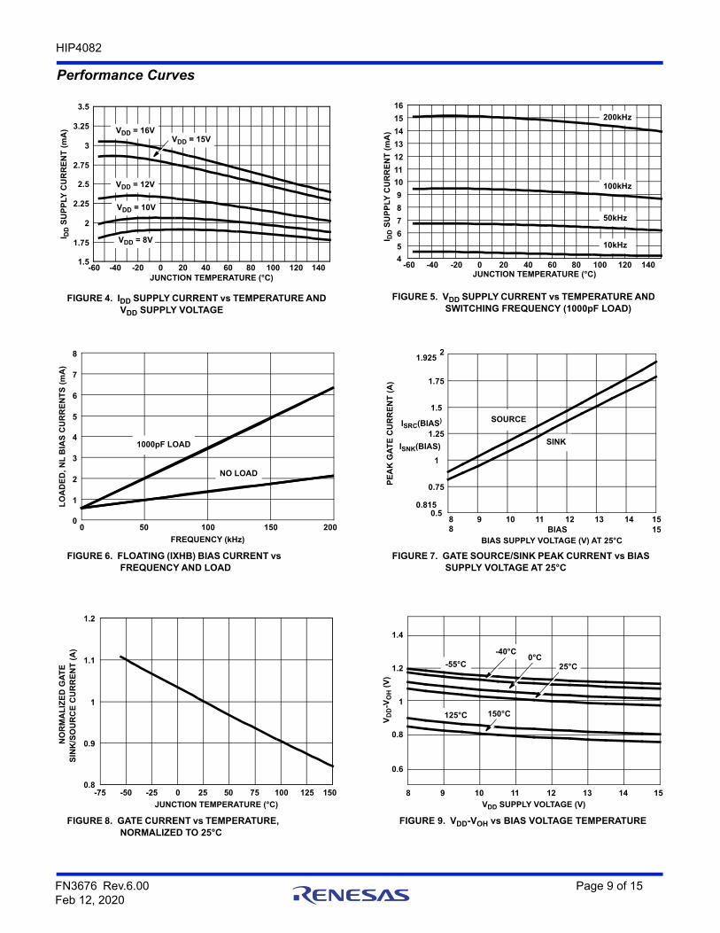
Performance Curves
FIGURE 4. IDD SUPPLY CURRENT vs TEMPERATURE AND VDD SUPPLY VOLTAGE
FIGURE 5. VDD SUPPLY CURRENT vs TEMPERATURE AND SWITCHING FREQUENCY (1000pF LOAD)
FIGURE 6. FLOATING (IXHB) BIAS CURRENT vs FREQUENCY AND LOAD
FIGURE 7. GATE SOURCE/SINK PEAK CURRENT vs BIAS SUPPLY VOLTAGE AT 25°C
FIGURE 8. GATE CURRENT vs TEMPERATURE, NORMALIZED TO 25°C
FIGURE 9. VDD-VOH vs BIAS VOLTAGE TEMPERATURE
-60 -40 -20 0 20 40 60 80 100 120 1401.5
1.75
2
2.25
2.5
2.75
3
3.25
3.5
JUNCTION TEMPERATURE (°C)
I DD
SU
PP
LY C
UR
RE
NT
(m
A) VDD = 16V
VDD = 15V
VDD = 12V
VDD = 10V
VDD = 8V
-60 -40 -20 0 20 40 60 80 100 120 1404
5
6
7
8
9
10
11
12
13
14
15
16
JUNCTION TEMPERATURE (°C)
I DD
SU
PP
LY C
UR
RE
NT
(m
A)
200kHz
100kHz
50kHz
10kHz
0 50 100 150 2000
1
2
3
4
5
6
7
8
FREQUENCY (kHz)
LO
AD
ED
, NL
BIA
S C
UR
RE
NT
S (
mA
)
1000pF LOAD
NO LOAD
8 9 10 11 12 13 14 150.5
0.75
1
1.25
1.5
1.75
BIAS SUPPLY VOLTAGE (V) AT 25°C
PE
AK
GA
TE
CU
RR
EN
T (
A)
1.925
0.815
ISRC(BIAS)
ISNK(BIAS)
BIAS
2
8 15
SOURCE
SINK
-75 -50 -25 0 25 50 75 100 125 1500.8
0.9
1
1.1
1.2
JUNCTION TEMPERATURE (°C)
NO
RM
AL
IZE
D G
AT
ES
INK
/SO
UR
CE
CU
RR
EN
T (
A)
8 9 10 11 12 13 14 15
0.6
1
1.4
VDD SUPPLY VOLTAGE (V)
VD
D-V
OH
(V
)
1.2
0.8
-55°C
-40°C0°C
25°C
125°C 150°C
FN3676 Rev.6.00 Page 9 of 15Feb 12, 2020

HIP4082
FIGURE 10. VOL vs BIAS VOLTAGE AND TEMPERATURE FIGURE 11. UNDERVOLTAGE TRIP VOLTAGES vs TEMPERATURE
FIGURE 12. UPPER LOWER TURN-ON/TURN-OFF PROPAGATION DELAY vs TEMPERATURE
FIGURE 13. UPPER/LOWER DIS(ABLE) TO TURN-ON/OFF vs TEMPERATURE (°C)
FIGURE 14. FULL BRIDGE LEVEL-SHIFT CURRENT vs FREQUENCY (kHz)
FIGURE 15. MAXIMUM POWER DISSIPATION vs AMBIENT TEMPERATURE
Performance Curves (Continued)
8 9 10 11 12 13 14
1.4
VDD SUPPLY VOLTAGE (V)
VO
L (
V)
15
1.2
0.8
0.6
-55°C-40°C 0°C 25°C
125°C
150°C
1
-60 -40 -20 0 20 40 60 80 100 120 140 1605
5.5
6
6.5
7
7.5
8
JUNCTION TEMPERATURE (°C)
VD
D, B
IAS
SU
PP
LY V
OLT
AG
E (
V) LOWER U/V RESET
LOWER U/V SET
UPPER U/V SET/RESET
-60 -40 -20 0 20 40 60 80 100 120 140 16020
30
40
50
60
70
80
90
100
JUNCTION TEMPERATURE (°C)
PR
OP
AG
AT
ION
DE
LA
YS
(n
s)
UPPER tON
UPPER tOFF
LOWER tON
LOWER tOFF
-60 -40 -20 0 20 40 60 80 100 120 140 16010
100
104
JUNCTION TEMPERATURE (°C)
DIS
TO
TU
RN
-ON
/OF
F T
IME
(n
s)
1000
DISHTON
DISHTOFF
DISLTONDISLOFF
0 20 40 60 80 1000.5
1
1.5
2
SWITCHING FREQUENCY (kHz)
LE
VE
L-S
HIF
T C
UR
RE
NT
(m
A)
-60 -30 0 30 60 90 120 1500
0.5
1
1.5
2
2.5
AMBIENT TEMPERATURE (°C)
TO
TAL
PO
WE
R D
ISS
IPA
TIO
N (
W)
SOIC
16 PIN DIP
QUIESCENT BIAS COMPONENT
FN3676 Rev.6.00 Page 10 of 15Feb 12, 2020

HIP4082
FIGURE 16. DEAD-TIME vs DEL RESISTANCE AND BIAS SUPPLY (VDD) VOLTAGE
FIGURE 17. MAXIMUM OPERATING PEAK AHS/BHS VOLTAGE vs TEMPERATURE
Performance Curves (Continued)
0 10 20 30 40 50 60 70 80 90 100100
1000
104
DEAD TIME RESISTANCE (k)
DE
AD
TIM
E (
ns
)
VDD = 12V
VDD = 9V
VDD = 15V
100 50 0 50 100 15070
75
80
85
90
TEMPERATURE (°C)
VX
HS-V
SS
FN3676 Rev.6.00 Page 11 of 15Feb 12, 2020
HIP4082
Revision HistoryThe revision history provided is for informational purposes only and is believed to be accurate, but not warranted. Please go to the web to make
sure that you have the latest revision.
DATE REVISION CHANGE
Feb 12, 2020 FN3676.6 Updated Ordering information table on page 2.Removed About Intersil section.Updated POD M16.15 to the latest revision, changes are as follows:
-Updated graphics to new standard layout, removing the dimension table.Updated disclaimer.
Sep 30, 2015 FN3676.5 Updated the Ordering Information Table on page 2.Added Revision History and About Intersil sections.
FN3676 Rev.6.00 Page 12 of 15Feb 12, 2020

HIP4082
Package Outline Drawings
NOTES:
1. Controlling Dimensions: INCH. In case of conflict between English and Metric dimensions, the inch dimensions control.
2. Dimensioning and tolerancing per ANSI Y14.5M-1982.
3. Symbols are defined in the “MO Series Symbol List” in Section 2.2 of Publication No. 95.
4. Dimensions A, A1 and L are measured with the package seated in JE-DEC seating plane gauge GS-3.
5. D, D1, and E1 dimensions do not include mold flash or protrusions. Mold flash or protrusions shall not exceed 0.010 inch (0.25mm).
6. E and are measured with the leads constrained to be perpendic-ular to datum .
7. eB and eC are measured at the lead tips with the leads unconstrained. eC must be zero or greater.
8. B1 maximum dimensions do not include dambar protrusions. Dambar protrusions shall not exceed 0.010 inch (0.25mm).
9. N is the maximum number of terminal positions.
10. Corner leads (1, N, N/2 and N/2 + 1) for E8.3, E16.3, E18.3, E28.3, E42.6 will have a B1 dimension of 0.030 - 0.045 inch (0.76 - 1.14mm).
eA-C-
CL
E
eA
C
eB
eC
-B-
E1INDEX
1 2 3 N/2
N
AREA
SEATING
BASEPLANE
PLANE
-C-
D1
B1B
e
D
D1
AA2
L
A1
-A-
0.010 (0.25) C AM B S
E16.3 (JEDEC MS-001-BB ISSUE D)16 LEAD DUAL-IN-LINE PLASTIC PACKAGE (PDIP)
SYMBOL
INCHES MILLIMETERS
NOTESMIN MAX MIN MAX
A - 0.210 - 5.33 4
A1 0.015 - 0.39 - 4
A2 0.115 0.195 2.93 4.95 -
B 0.014 0.022 0.356 0.558 -
B1 0.045 0.070 1.15 1.77 8, 10
C 0.008 0.014 0.204 0.355 -
D 0.735 0.775 18.66 19.68 5
D1 0.005 - 0.13 - 5
E 0.300 0.325 7.62 8.25 6
E1 0.240 0.280 6.10 7.11 5
e 0.100 BSC 2.54 BSC -
eA 0.300 BSC 7.62 BSC 6
eB - 0.430 - 10.92 7
L 0.115 0.150 2.93 3.81 4
N 16 16 9
Rev. 0 12/93
FN3676 Rev.6.00 Page 13 of 15Feb 12, 2020

HIP4082
M16.15 (JEDEC MS-012-AC ISSUE C)16 LEAD NARROW BODY SMALL OUTLINE PLASTIC PACKAGE Rev 2, 11/17
FN3676 Rev.6.00 Page 14 of 15Feb 12, 2020

Corporate HeadquartersTOYOSU FORESIA, 3-2-24 Toyosu,Koto-ku, Tokyo 135-0061, Japanwww.renesas.com
Contact InformationFor further information on a product, technology, the most up-to-date version of a document, or your nearest sales office, please visit:
www.renesas.com/contact/
TrademarksRenesas and the Renesas logo are trademarks of Renesas Electronics Corporation. All trademarks and registered trademarks are the property of their respective owners.
© 2020 Renesas Electronics Corporation. All rights reserved.