Embed Size (px)
Citation preview
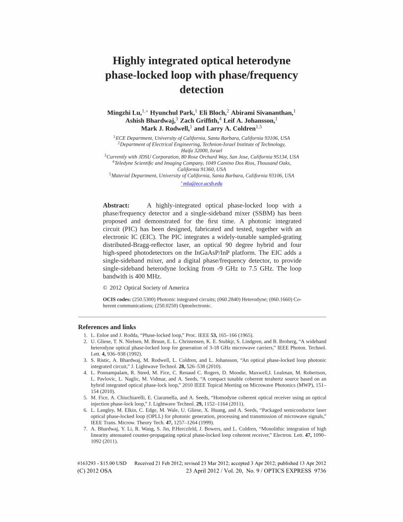
Highly integrated optical heterodynephase-locked loop with phase/frequency
detection
Mingzhi Lu,1,∗ Hyunchul Park,1 Eli Bloch,2 Abirami Sivananthan,1
Ashish Bhardwaj,3 Zach Griffith,4 Leif A. Johansson,1
Mark J. Rodwell,1 and Larry A. Coldren1,5
1ECE Department, University of California, Santa Barbara, California 93106, USA2Department of Electrical Engineering, Technion-Israel Institute of Technology,
Haifa 32000, Israel3Currently with JDSU Corporation, 80 Rose Orchard Way, San Jose, California 95134, USA
4Teledyne Scientific and Imaging Company, 1049 Camino Dos Rios, Thousand Oaks,California 91360, USA
5Material Department, University of California, Santa Barbara, California 93106, USA∗[email protected]
Abstract: A highly-integrated optical phase-locked loop with aphase/frequency detector and a single-sideband mixer (SSBM) has beenproposed and demonstrated for the first time. A photonic integratedcircuit (PIC) has been designed, fabricated and tested, together with anelectronic IC (EIC). The PIC integrates a widely-tunable sampled-gratingdistributed-Bragg-reflector laser, an optical 90 degree hybrid and fourhigh-speed photodetectors on the InGaAsP/InP platform. The EIC adds asingle-sideband mixer, and a digital phase/frequency detector, to providesingle-sideband heterodyne locking from -9 GHz to 7.5 GHz. The loopbandwith is 400 MHz.
© 2012 Optical Society of America
OCIS codes: (250.5300) Photonic integrated circuits; (060.2840) Heterodyne; (060.1660) Co-herent communications; (250.0250) Optoelectronic.
References and links1. L. Enloe and J. Rodda, “Phase-locked loop,” Proc. IEEE 53, 165–166 (1965).2. U. Gliese, T. N. Nielsen, M. Bruun, E. L. Christensen, K. E. Stubkjr, S. Lindgren, and B. Broberg, “A wideband
heterodyne optical phase-locked loop for generation of 3-18 GHz microwave carriers,” IEEE Photon. Technol.Lett. 4, 936–938 (1992).
3. S. Ristic, A. Bhardwaj, M. Rodwell, L. Coldren, and L. Johansson, “An optical phase-locked loop photonicintegrated circuit,” J. Lightwave Technol. 28, 526–538 (2010).
4. L. Ponnampalam, R. Steed, M. Fice, C. Renaud C. Rogers, D. Moodie, Maxwell,I. Lealman, M. Robertson,L. Pavlovic, L. Naglic, M. Vidmar, and A. Seeds, “A compact tunable coherent terahertz source based on anhybrid integrated optical phase-lock loop,” 2010 IEEE Topical Meeting on Microwave Photonics (MWP), 151–154 (2010).
5. M. Fice, A. Chiuchiarelli, E. Ciaramella, and A. Seeds, “Homodyne coherent optical receiver using an opticalinjection phase-lock loop,” J. Lightwave Technol. 29, 1152–1164 (2011).
6. L. Langley, M. Elkin, C. Edge, M. Wale, U. Gliese, X. Huang, and A. Seeds, “Packaged semiconductor laseroptical phase-locked loop (OPLL) for photonic generation, processing and transmission of microwave signals,”IEEE Trans. Microw. Theory Tech. 47, 1257–1264 (1999).
7. A. Bhardwaj, Y. Li, R. Wang, S. Jin, P.Herczfeld, J. Bowers, and L. Coldren, “Monolithic integration of highlinearity attenuated counter-propagating optical phase-locked loop coherent receiver,” Electron. Lett. 47, 1090–1092 (2011).
#163293 - $15.00 USD Received 21 Feb 2012; revised 23 Mar 2012; accepted 3 Apr 2012; published 13 Apr 2012(C) 2012 OSA 23 April 2012 / Vol. 20, No. 9 / OPTICS EXPRESS 9736
8. P. Binetti , M. Lu, E. Norberg, R. Guzzon, J. Parker, A. Sivananthan, A. Bhardwaj, L. Johansson, M. Rodwell,and L. Coldren, “Indium phosphide photonic integrated circuits for coherent optical links,” IEEE J. QuantumElectron. 48, 279–291 (2012).
9. N. Satyan, A. Vasilyev, G. Rakuljic, V. Leyva, and A. Yariv, ”Precise control of broadband frequency chirps usingoptoelectronic feedback,” Opt. Express 17, 15991–15999 (2009).
10. M. Lu, A. Bhardwaj, A. Sivananthan, L. Johansson, H. Park, E. Bloch, M. Rodwell, and L. Coldren, “Widely-tunable integrated coherent optical receiver using a phase-locked loop,” IEEE Photonics Conf., Arlington, VA,ThL4 (2011).
11. N. Satyan , W. Liang, and A. Yariv, “Coherence cloning using semiconductor laser optical phase-lock loops,”IEEE J. Quantum Electron. 45, 755–761 (2009).
12. N. Satyan, W. Liang, A. Kewitsch, G. Rakuljic, and A. Yariv, “Coherent power combination of semiconductorlasers using optical phase lock loops,” IEEE J. Sel. Top. Quantum Electron. 15, 240–247 (2009).
13. R. Steed, F. Pozzi, M. Fice, C. Renaud, D. Rogers, I. Lealman, D. Moodie, P. Cannard, C. Lynch, L. Johnston, M.Robertson, R. Cronin, L. Pavlovic, L. Naglic, M. Vidmar, and A. Seeds, “Monolithically integrated heterodyneoptical phase-lock loop with RF XOR phase detector,” Opt. Express 19, 20048–20053 (2011).
14. E. Bloch, H. Park, M. Lu, T. Reed, Z. Griffith, L. Johansson, L. Coldren, D. Ritter, and M. Rodwell, “A 1-20GHz InP HBT phase-lock-loop IC for optical wavelength synthesis,” Accepted by IEEE Int. Micro. Symposium(2012).
15. L. Coldren, “Monolithic tunable diode lasers,” IEEE J. Sel. Top. Quantum Electron. 6, 988–999 (2000).16. C. Doerr, D. Gill, A. Gnauck, L. Buhl, P. Winzer, M. Cappuzzo, A. Wong-Foy, E. Chen, and L. Gomez, “Mono-
lithic demodulator for 40-Gb/s DQPSK using a star coupler,” J. Lightwave Technol. 24, 171–174 (2006).17. D. Messerschmitt, “Frequency detectors for PLL acquisition in timing and carrier recovery,” IEEE Trans. Com-
mun. 27, 1288–1295 (1979).18. J. Raring, M.Sysak, A. Pedretti, M. Dummer, E. Skogen, J. Barton, S. Denbaars, and L. Coldren, “Advanced
integration schemes for high-functionality/high-performance photonic integrated circuits,” in Proc. IEEE SPIE,San Jose, CA, Paper 6126-19 (2006).
19. E. Skogen, J. Barton, S. Denbaars, and L. Coldren, “A quantum-well-intermixing process for wavelength-agilephotonic integrated circuits,” IEEE J. Sel. Top. Quantum Electron. 8, 863–869 (2002).
1. Introduction
Ever since the first demonstration of optical phase-locked loops (OPLL) [1], significant ef-fort has been devoted for a wide range applications, as described in Ref. [2–7] and referencestherein. An OPLL is highly desirable for many applications, such as continuous-wave (CW)chirped LIDAR [4, 8, 9], coherent receivers [5, 7, 10], laser linewidth narrowing and “cloning”of another laser’s properties [11, 12], and millimeter wave generation [4, 6].
Recent progress on heterodyne optical phase locking can be found in Ref. [3, 13]. By usingan on-PIC modulator or an RF mixer, heterodyne locking can be achieved with a phase detector.However, without any frequency pull-in, the offset frequency cannot be easily tuned, and thelocking range is limited. Every time the RF reference frequency is reset, either the master laseror slave laser in this OPLL needs to be adjusted to make sure the free running offset frequencyis within the pull-in range of the phase-locked loop, which is normally several hundred MHzat most. Moreover, the loop cannot differentiate the sign of the frequency offset for heterodynelocking. In other words, there are two stable locking points for the heterodyne locking, one isat Δ f > 0, and the other is at Δ f < 0, where Δ f is defined as follow.
Δ f = fre f − fslave (1)
In this work, we propose and demonstrate a new architecture of OPLL with both phaseand frequency detection and a single-sideband mixer (SSBM) [14], which enable large-rangefrequency pull-in and offset frequency tuning within tens of GHz. We successfully achievedheterodyne locking from -9 GHz to 7.5 GHz, where the offset frequency is defined in Eq. (1).
In terms of OPLL design, one of the most important issues is loop delay. Considering thelinewidth and the stability of the on-PIC slave laser, and the frequency pull-in error [14], a300 MHz loop bandwidth is demanded as a minimum for stable phase locking. To achievefull functionality and keep a relatively short loop delay, a photonic integrated circuit (PIC) is
#163293 - $15.00 USD Received 21 Feb 2012; revised 23 Mar 2012; accepted 3 Apr 2012; published 13 Apr 2012(C) 2012 OSA 23 April 2012 / Vol. 20, No. 9 / OPTICS EXPRESS 9737
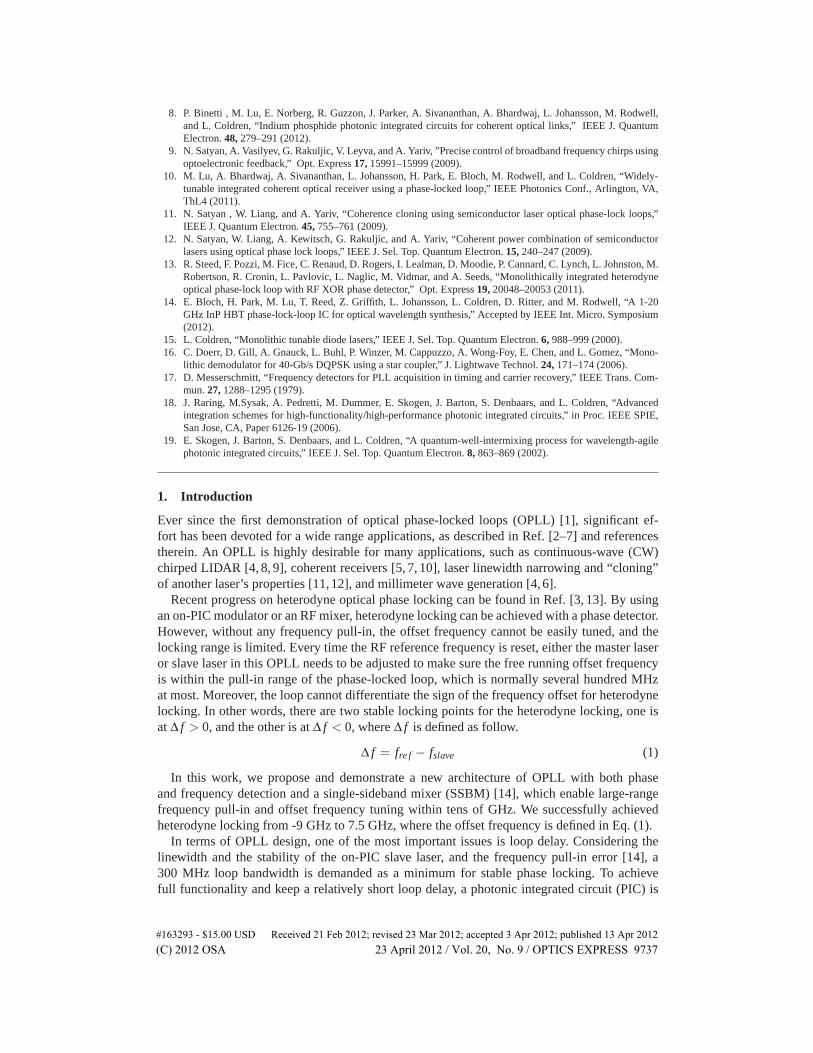
desired, as well as a high-speed electronic IC (EIC) and a carefully designed loop filter (LF).The architecture of the system is shown in Fig. 1. It is designed to be a second order phase-locked loop. The designed phase margin is 65 degree, and the amplitude margin is 7 dB.
On the PIC, we integrated a widely-tunable sampled-grating distributed-Bragg-reflector (SG-DBR) laser [15], a star-coupler-based optical 90 degree hybrid [16], four single-ended high-speed quantum well photodetectors, and microstrip transmission lines. The SG-DBR laser actsas the widely-tunable slave laser. By injecting current into the back and front mirrors, the reflec-tion spectrum vernier can be tuned so that the laser can cover a 40 nm range. Meanwhile, thecurrent injection into the phase section can tune the laser wavelength finely within one cavitymode, which is around 40 GHz.
The reference laser and the SG-DBR slave laser are mixed in the optical 90 degree hybrid.In-phase and quadrature signals are then generated, which are used for single-sideband mixingand phase/frequency detection. As for the 90 degree hybrid design, a 2-by-4 star coupler isused. We calculated a 2.3 degree error across 40 nm, and estimated about 4 dB loss. On each ofthe star coupler output waveguides, there is a 50 μm - by - 3 μm p-i-n waveguide photodetector.The electrical signal from the four photodetectors are led to the same side of the PIC using four430 μm long miscrostrip transmission lines for PIC-EIC interconnection. Bisbenzocyclobutene(BCB) is used as the dielectric between the signal lines and the RF ground. The RF pads on thePIC have the same pitch size as those on the EIC in order to assemble the PIC and EIC togetherfor system testing.
Fig. 1. The architecture of the OPLL.
On this EIC, transimpedance limiting amplifiers, a delay line, an XOR gate and a single-sideband mixer (SSBM) were integrated. The delay line and the XOR gate together act as aphase/frequency detector [14, 17]. The loop filter is a hybrid circuit built on an AluminiumNitride carrier, using a voltage feedback operational amplifier as an active filter and integrator.The beating signal from the on-PIC photodetectors are finally negatively fed back to the SG-DBR laser phase section through the EIC and the loop filter.
The loop delay of this OPLL is approximately 200 ps, in which 40 ps is from the PIC, >100ps is from the EIC and 50 ps from the LF and interconnections between them.
2. Fabrication
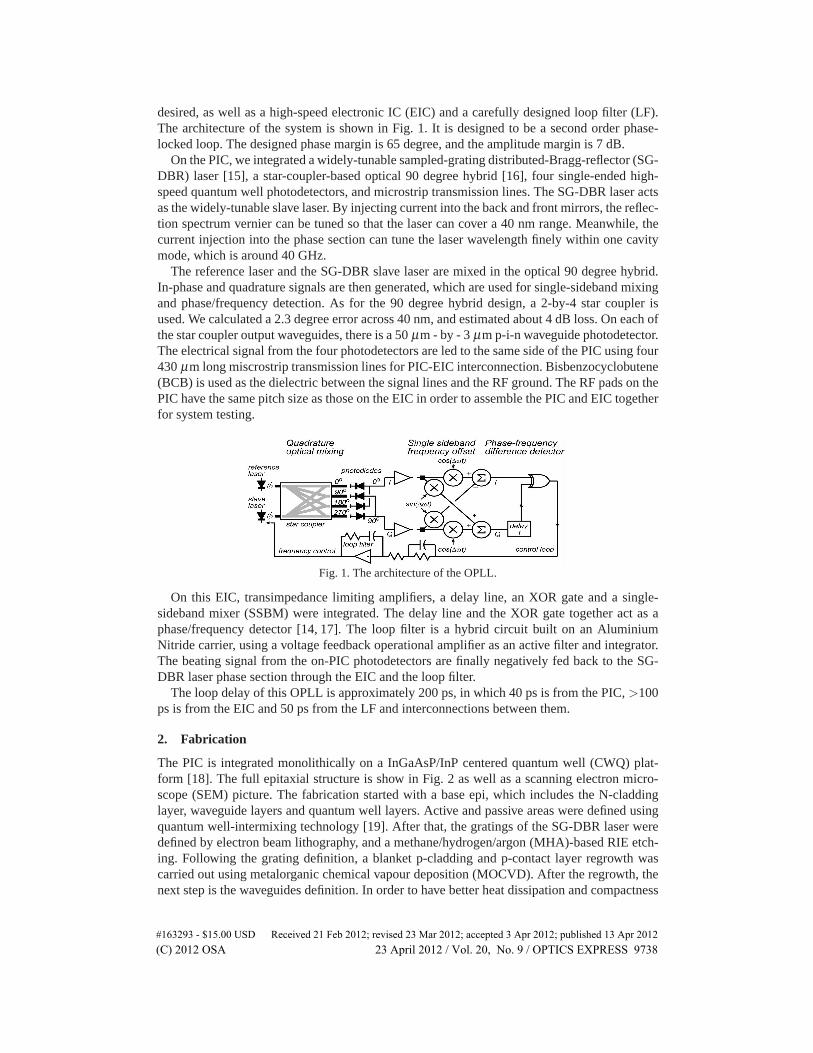
The PIC is integrated monolithically on a InGaAsP/InP centered quantum well (CWQ) plat-form [18]. The full epitaxial structure is show in Fig. 2 as well as a scanning electron micro-scope (SEM) picture. The fabrication started with a base epi, which includes the N-claddinglayer, waveguide layers and quantum well layers. Active and passive areas were defined usingquantum well-intermixing technology [19]. After that, the gratings of the SG-DBR laser weredefined by electron beam lithography, and a methane/hydrogen/argon (MHA)-based RIE etch-ing. Following the grating definition, a blanket p-cladding and p-contact layer regrowth wascarried out using metalorganic chemical vapour deposition (MOCVD). After the regrowth, thenext step is the waveguides definition. In order to have better heat dissipation and compactness
#163293 - $15.00 USD Received 21 Feb 2012; revised 23 Mar 2012; accepted 3 Apr 2012; published 13 Apr 2012(C) 2012 OSA 23 April 2012 / Vol. 20, No. 9 / OPTICS EXPRESS 9738
(a) (b)
Fig. 2. Epitaxial structure of the integration platform. (a) shows the schematic illustration ofthe CQW InGaAsP/InP platform for active/passive device integration. (b) shows the crosssection of a waveguide.
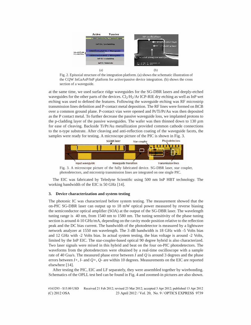
at the same time, we used surface ridge waveguides for the SG-DBR lasers and deeply-etchedwaveguides for the other parts of the devices. Cl2/H2/Ar ICP-RIE dry etching as well as InP wetetching was used to defined the features. Following the waveguide etching was RF microstriptransmission lines definition and P-contact metal deposition. The RF lines were formed on BCBover a common ground plane. P-contact vias were opened and Pt/Ti/Pt/Au was then depositedas the P contact metal. To further decrease the passive waveguide loss, we implanted protons tothe p-cladding layer of the passive waveguides. The wafer was then thinned down to 130 μmfor ease of cleaving. Backside Ti/Pt/Au metallization provided common cathode connectionsto the n-type substrate. After cleaving and anti-reflection coating of the waveguide facets, thesamples were ready for testing. A microscope picture of the PIC is shown in Fig. 3.
Fig. 3. A microscope picture of the fully fabricated device. SG-DBR laser, star coupler,photodetectors, and microstrip transmission lines are integrated on one single PIC.
The EIC was fabricated by Teledyne Scientific using 500 nm InP HBT technology. Theworking bandwidth of the EIC is 50 GHz [14].
3. Device characterization and system testing
The photonic IC was characterized before system testing. The measurement showed that theon-PIC SG-DBR laser can output up to 18 mW optical power measured by reverse biasingthe semiconductor optical amplifier (SOA) at the output of the SG-DBR laser. The wavelengthtuning range is 40 nm, from 1540 nm to 1580 nm. The tuning sensitivity of the phase tuningsection is around 4-10 GHz/mA, depending on the cavity mode position relative to the reflectionpeak and the DC bias current. The bandwidth of the photodetector is measured by a lightwavenetwork analyzer at 1550 nm wavelength. The 3 dB bandwidth is 18 GHz with -5 Volts biasand 12 GHz with -2 Volts bias. In actual system testing, the bias voltage is around -2 Volts,limited by the InP EIC. The star-coupler-based optical 90 degree hybrid is also characterized.Two laser signals were mixed in this hybrid and beat on the four on-PIC photodetectors. Thewaveforms from the photodetectors were obtained by a real-time oscilloscope with a samplerate of 40 Gsa/s. The measured phase error between I and Q is around 3 degrees and the phaseerrors between I+, I- and Q+, Q- are within 10 degrees. Measurements on the EIC are reportedelsewhere [14].
After testing the PIC, EIC and LF separately, they were assembled together by wirebonding.Schematics of the OPLL test bed can be found in Fig. 4 and zoomed-in pictures are also shown.
#163293 - $15.00 USD Received 21 Feb 2012; revised 23 Mar 2012; accepted 3 Apr 2012; published 13 Apr 2012(C) 2012 OSA 23 April 2012 / Vol. 20, No. 9 / OPTICS EXPRESS 9739
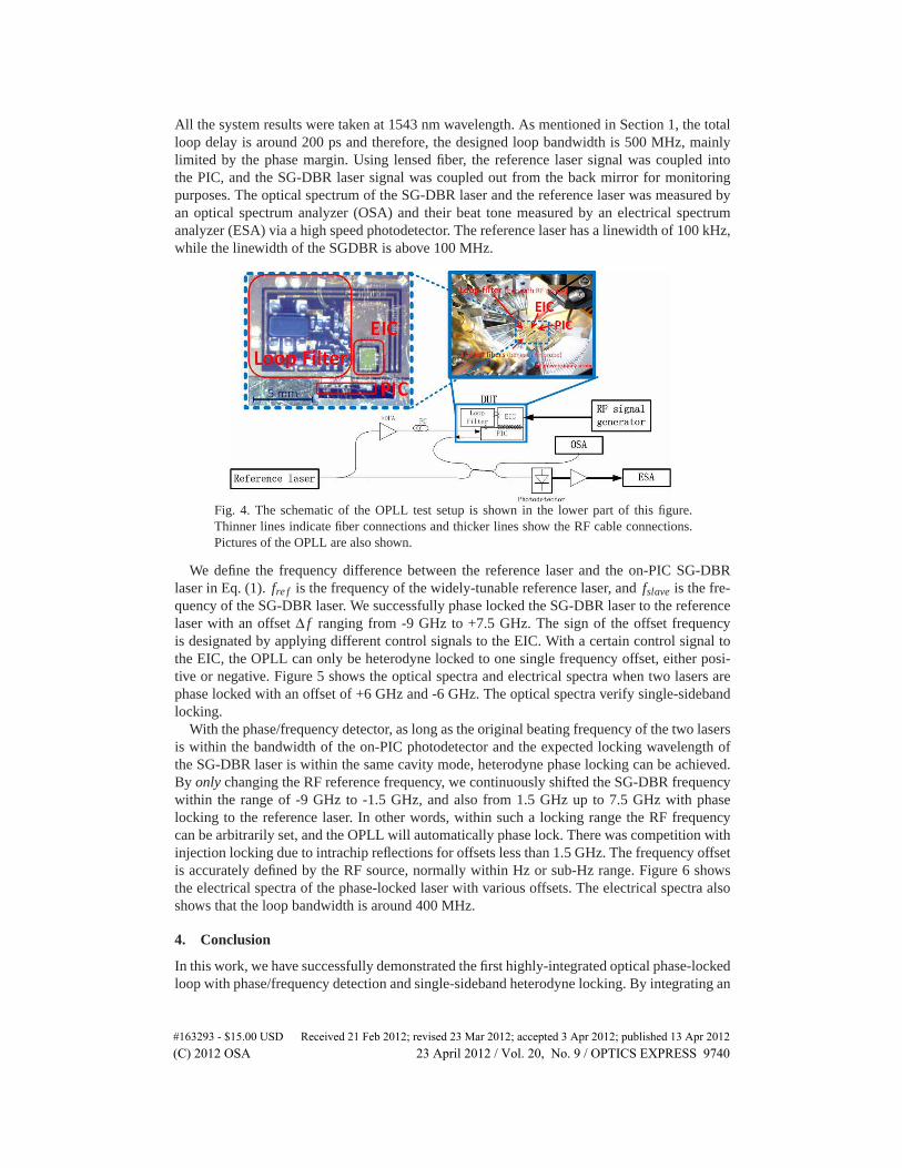
All the system results were taken at 1543 nm wavelength. As mentioned in Section 1, the totalloop delay is around 200 ps and therefore, the designed loop bandwidth is 500 MHz, mainlylimited by the phase margin. Using lensed fiber, the reference laser signal was coupled intothe PIC, and the SG-DBR laser signal was coupled out from the back mirror for monitoringpurposes. The optical spectrum of the SG-DBR laser and the reference laser was measured byan optical spectrum analyzer (OSA) and their beat tone measured by an electrical spectrumanalyzer (ESA) via a high speed photodetector. The reference laser has a linewidth of 100 kHz,while the linewidth of the SGDBR is above 100 MHz.
Fig. 4. The schematic of the OPLL test setup is shown in the lower part of this figure.Thinner lines indicate fiber connections and thicker lines show the RF cable connections.Pictures of the OPLL are also shown.
We define the frequency difference between the reference laser and the on-PIC SG-DBRlaser in Eq. (1). fre f is the frequency of the widely-tunable reference laser, and fslave is the fre-quency of the SG-DBR laser. We successfully phase locked the SG-DBR laser to the referencelaser with an offset Δ f ranging from -9 GHz to +7.5 GHz. The sign of the offset frequencyis designated by applying different control signals to the EIC. With a certain control signal tothe EIC, the OPLL can only be heterodyne locked to one single frequency offset, either posi-tive or negative. Figure 5 shows the optical spectra and electrical spectra when two lasers arephase locked with an offset of +6 GHz and -6 GHz. The optical spectra verify single-sidebandlocking.
With the phase/frequency detector, as long as the original beating frequency of the two lasersis within the bandwidth of the on-PIC photodetector and the expected locking wavelength ofthe SG-DBR laser is within the same cavity mode, heterodyne phase locking can be achieved.By only changing the RF reference frequency, we continuously shifted the SG-DBR frequencywithin the range of -9 GHz to -1.5 GHz, and also from 1.5 GHz up to 7.5 GHz with phaselocking to the reference laser. In other words, within such a locking range the RF frequencycan be arbitrarily set, and the OPLL will automatically phase lock. There was competition withinjection locking due to intrachip reflections for offsets less than 1.5 GHz. The frequency offsetis accurately defined by the RF source, normally within Hz or sub-Hz range. Figure 6 showsthe electrical spectra of the phase-locked laser with various offsets. The electrical spectra alsoshows that the loop bandwidth is around 400 MHz.
4. Conclusion
In this work, we have successfully demonstrated the first highly-integrated optical phase-lockedloop with phase/frequency detection and single-sideband heterodyne locking. By integrating an
#163293 - $15.00 USD Received 21 Feb 2012; revised 23 Mar 2012; accepted 3 Apr 2012; published 13 Apr 2012(C) 2012 OSA 23 April 2012 / Vol. 20, No. 9 / OPTICS EXPRESS 9740
1542.8 1542.9 1543 1543.1 1543.2 1543.3 1543.4−80
−60
−40
−20
0
Wavelength / nm
Spect
rum
inte
nsi
ty / dB
m
(a)
1542.8 1542.9 1543 1543.1 1543.2 1543.3 1543.4−80
−60
−40
−20
0
Wavelength / nm
Sp
ect
rum
inte
nsi
ty
/ d
Bm
(b)
5.5 6 6.5
−60
−40
−20
0
Frequency / GHz
Sp
ect
rum
inte
nsi
ty
/ d
Bm
(c)
−6.5 −6 −5.5
−60
−40
−20
0
Frequency / GHz
Sp
ect
rum
inte
nsi
ty
/ d
Bm
(d)
Fig. 5. (a) and (b) show the optical spectrums when two lasers are phase locked with afrequency difference of +6 GHz and -6 GHz. The reference laser has the higher power. (c)and (d) show the beating tones of the two laser when the offset frequency are +6 GHz and-6 GHz respectively, measured with 5 kHz resolution bandwidth.
−10 −9 −8 −7 −6 −5 −4 −3 −2 −1−60
−40
−20
0
Frequency / GHz
Nor
mal
ized
inte
nsity
/ d
B
1 2 3 4 5 6 7 8 9
−60
−40
−20
0
Frequency / GHz
Nor
mal
ized
inte
nsity
/ d
B
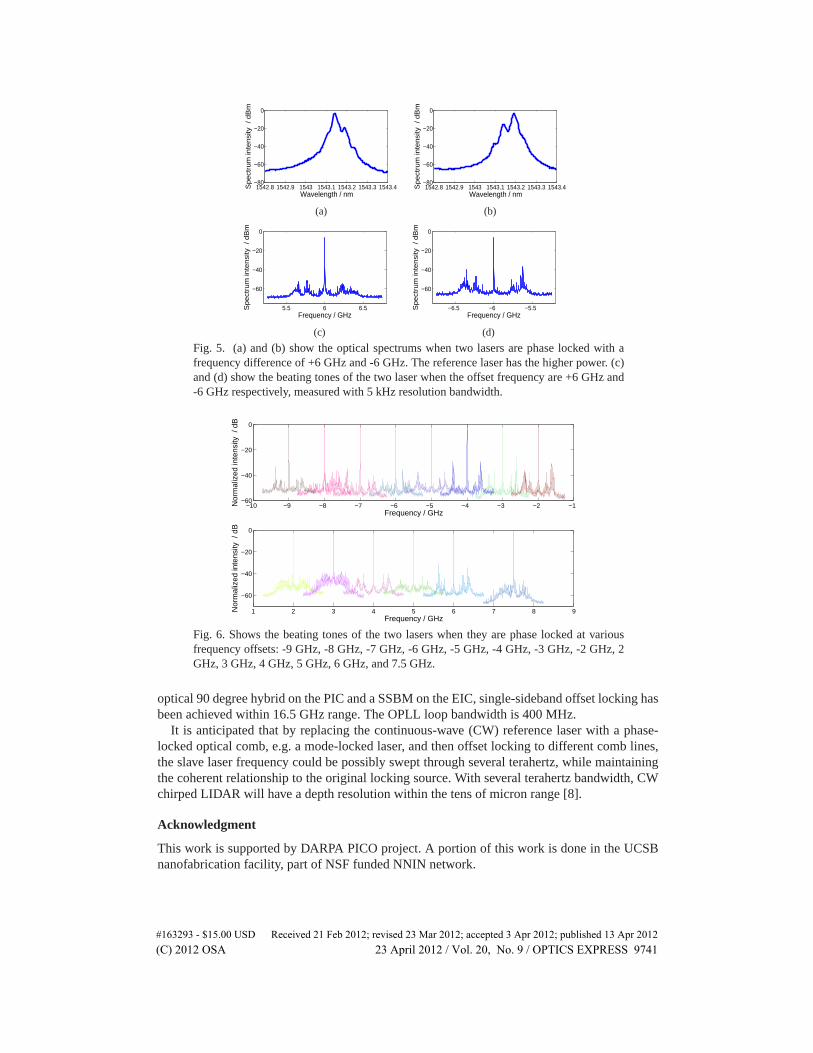
Fig. 6. Shows the beating tones of the two lasers when they are phase locked at variousfrequency offsets: -9 GHz, -8 GHz, -7 GHz, -6 GHz, -5 GHz, -4 GHz, -3 GHz, -2 GHz, 2GHz, 3 GHz, 4 GHz, 5 GHz, 6 GHz, and 7.5 GHz.
optical 90 degree hybrid on the PIC and a SSBM on the EIC, single-sideband offset locking hasbeen achieved within 16.5 GHz range. The OPLL loop bandwidth is 400 MHz.
It is anticipated that by replacing the continuous-wave (CW) reference laser with a phase-locked optical comb, e.g. a mode-locked laser, and then offset locking to different comb lines,the slave laser frequency could be possibly swept through several terahertz, while maintainingthe coherent relationship to the original locking source. With several terahertz bandwidth, CWchirped LIDAR will have a depth resolution within the tens of micron range [8].
Acknowledgment
This work is supported by DARPA PICO project. A portion of this work is done in the UCSBnanofabrication facility, part of NSF funded NNIN network.
#163293 - $15.00 USD Received 21 Feb 2012; revised 23 Mar 2012; accepted 3 Apr 2012; published 13 Apr 2012(C) 2012 OSA 23 April 2012 / Vol. 20, No. 9 / OPTICS EXPRESS 9741