Embed Size (px)
Citation preview
1
Highly efficient blue polyfluorene-based polymer light - emitting diodes
through solvent vapor annealing
T. Zhang, Y. Deng, S. Johnson and G. Liu*
Environmental Energy Technologies Division,
Lawrence Berkeley National Laboratory, Berkeley, CA 94720
Abstract
A highly efficient blue polymer light emitting diode based on [poly(9,9-di(2-(2-(2-
methoxy-ethoxy)ethoxy)ethyl)fluorenyl-2,7-diyl)] (PFOEO3) by solvent vapor annealing
the polymer emitting layer is fabricated in a bi-layer device with the Al cathode. High
electroluminescent efficiency is achieved by balancing charge injection. Better contact
interface between polymer and cathode formed by making chain conformation reoriented
with solvent vapor exposure. The effect of solvent vapor exposure on the potential barrier
height of the interface is estimated using the Richardson-Schottky model. The maximum
efficiency achieved 2.3 cd/A of the vapor exposed device from 0.9cd/A of the untreated
pristine device.
*Corresponding Author: Phone: (510) 486-7207; fax: (510) 486-7303;
email: [email protected]
2
1.Introduction
Conjugated polymer electroluminescence (EL) has been extensively studied for its
applications in optoelectronic devices since the original report by Burroughes et al.[1]
The solution based fabrication process for the polymer organic light emitting diode
(OLED) has been recognized as a major advantage compared to the vacuum deposition
process for small molecule OLED device. However, one major problem faced in the
development of polymer light-emitting diodes is that of unbalanced carrier transport. One
option is to use multi-layer devices with charge-injection or transporting layer. One
limitation imposed by the solution process is layer mixing during the coating process for
multilayered devices. One strategy is to render the layer insoluble by chemically
crosslinking prior to the application of the next layer. However this approach not only
drives up the cost but also in many cases is impractical. A widely used method is the use
of a non-mixing solvent for each layer, such as aqueous suspension of poly(3,4-
ethylenedioxythiophene):poly(sodium 4-styrenesulfonate) (PEDOT:PSS) for the hole
injection layer and an organic based solution for light emitting layer. However, it is
impossible to find a solvent system that does not affect the aqueous deposited layer and
the organic solution deposited layer for additional solution based deposition. Therefore
most of the practical polymer devices are bilayer device with a hole transport
PEDOT:PSS layer and light emitting layer. Hence, there is currently no practical strategy
to improve the electron injection for a given light emitting polymer system other than
using a low work function cathode, such as alkaline earth metals.
Among the large class of semiconductive organic conjugated polymers, polyfluorene
(PFO) and its based copolymers are the most promising for electroluminescent
3
applications.[2-5] Besides the excellent optical properties and suitable HOMO/LUMO
energy levels, PFOs possess excellent charge-transport properties, with hole mobility (10-
4 cm2/Vs) more than an order of magnitude higher than that of the poly(p-
phenylenevinylene) (10-5 cm2/Vs).[6-9] However, they still suffer from low EL efficiency
due to the imbalance of charge carriers. The electron mobility and injection is much more
critical than those of holes.[10] Therefore improved electron injection is critical to
improving the efficiency of the PFO based OLED device.[11] The arrangements of the
side chain and conjugated backbone significantly affects the interfacial
characteristics.[12-14] Here, the aim of this work is to modify the interface of the light
emitting polymer film and cathode to significantly improve the performance of an OLED
device by solvent annealing technique. This technology is not only conformable to
solution based process but also adaptable to roll-to-roll production method. We suggest
that the solvent vapor approach is a general and cost-effective method of improving the
colour purity and efficiency from polyfluorene-based light emitting devices. The
reorientation of polymer chains improves the electron injection at the polymer cathode
interface but also roles as holes trap to balance the charge injection. The resulting device
has an enhanced efficiency of 2.3 cd/A at 6 V from 0.9 cd/A for the pristine device. Such
performance is already among the highest ever report of polyfluorene homopolymers
with the single layer with Al cathode.
2. Experimental
The light emitting homopolymer poly(9,9-di(2-(2-(2-methoxy-
ethoxy)ethoxy)ethyl)fluorenyl-2,7-diyl) (PFOEO3) with Mw 64,000 Dalton and
polydispersity 7.4 was purchased from America Dye Source Inc. The molecular structure
4
is shown in the inset of Figure 1. PFOEO3 was dissolved in chlorobenzene and spin coat
onto the PEDOT:PSS coated ITO glass substrates. The PFOEO3 films were exposed in
toluene vapor for 1 hour and 5 hour respectively at 25 °C. Aluminum (Al) layer were
evaporated on the PFO film surface under a base pressure of 10-6 Torr. The final OLED
device configuration is ITO/PEDOT:PSS/PFOEO3/Al. J-V characteristics were measured
using Keithley 2420 source-measure unit. Luminance measurements were performed
using a LS-110 model Minolta luminance meter.
3. Results and dission
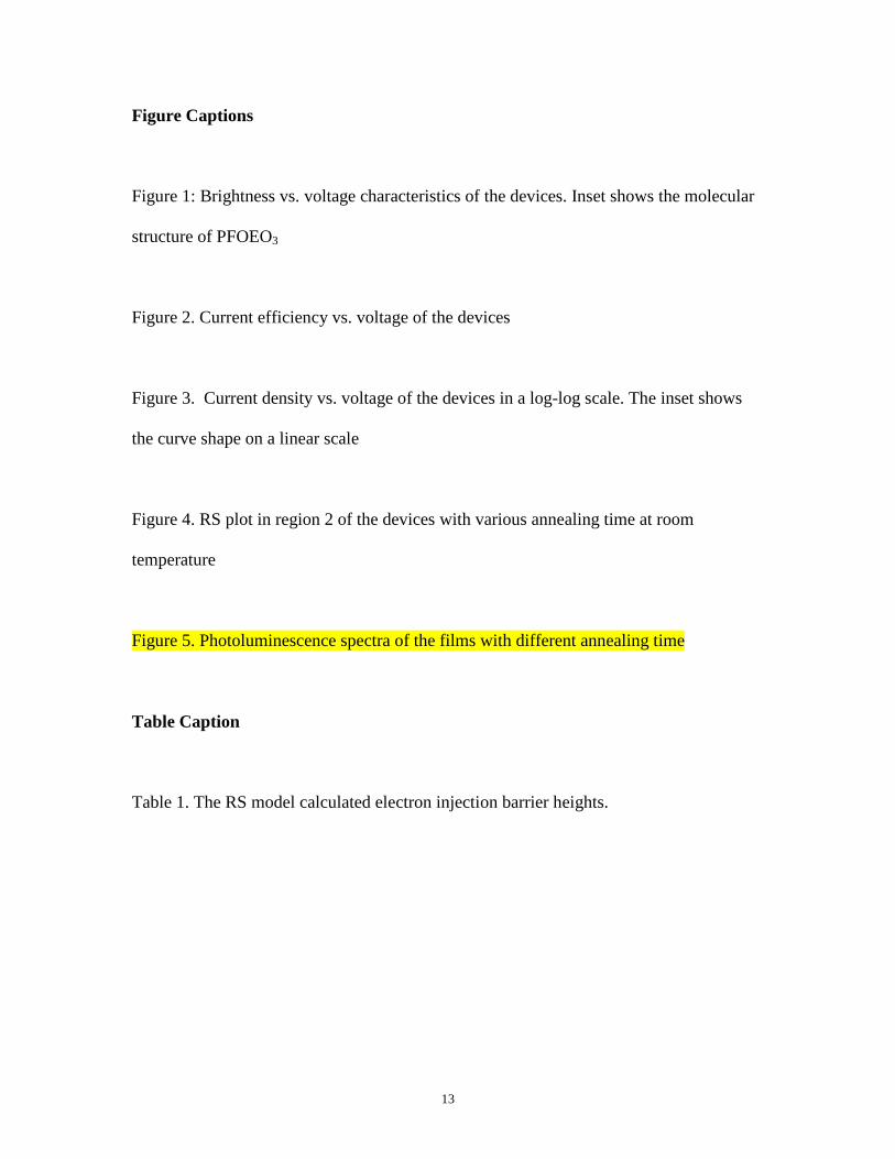
Figure 1 shows the Brightness-Voltage characteristics of the bilayer polymer
OLEDs of the untreated device and two vapor annealed devices. The device fabricated
with untreated PFO film is designated as pristine device. The brightness of the devices at
the same driving voltage is very dependent upon the annealing conditions, demonstrating
that the longer the vapor annealing time, the higher the brightness at a given voltage. The
pristine device shows 925 cd/m2 at 8V, whereas 1356 cd/m2 and 1498 cd/m2 under the
same voltage when the films were annealed in toluene vapor for 1 hour and 5 hours,
respectively. It is found that the turn-on light-emission voltages of the vapor annealed
devices are lower than that of the pristine device.[13] The device that was vapor annealed
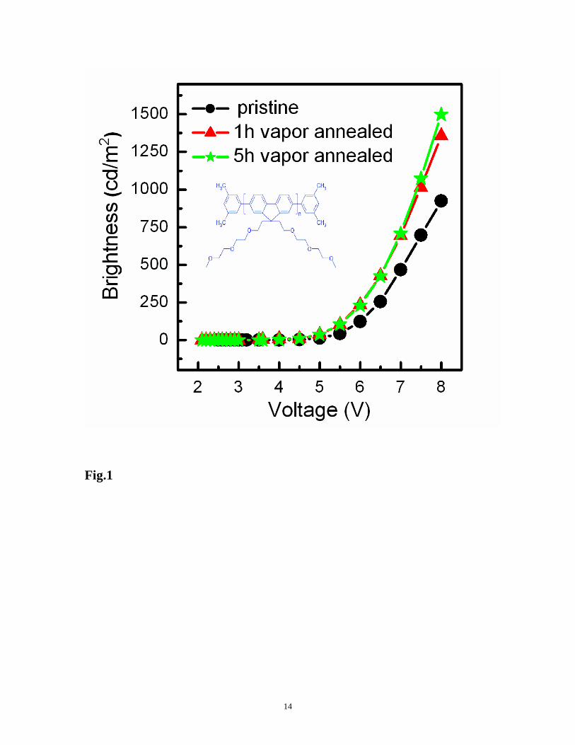
for 5 hours with the Al cathode shows a maximum luminous efficiency of 2.3 cd/A at 6 V,
much higher than 0.9 cd/A of the pristine device at 7.5 V as shown in Figure 2. This
performance is among the most efficient blue PLEDs based on polyfluorenes. This
implies that vapor annealing may facilitate the efficient electron injection at PFO/Al
interface, since the film surface was affected by the solvent annealing before Al
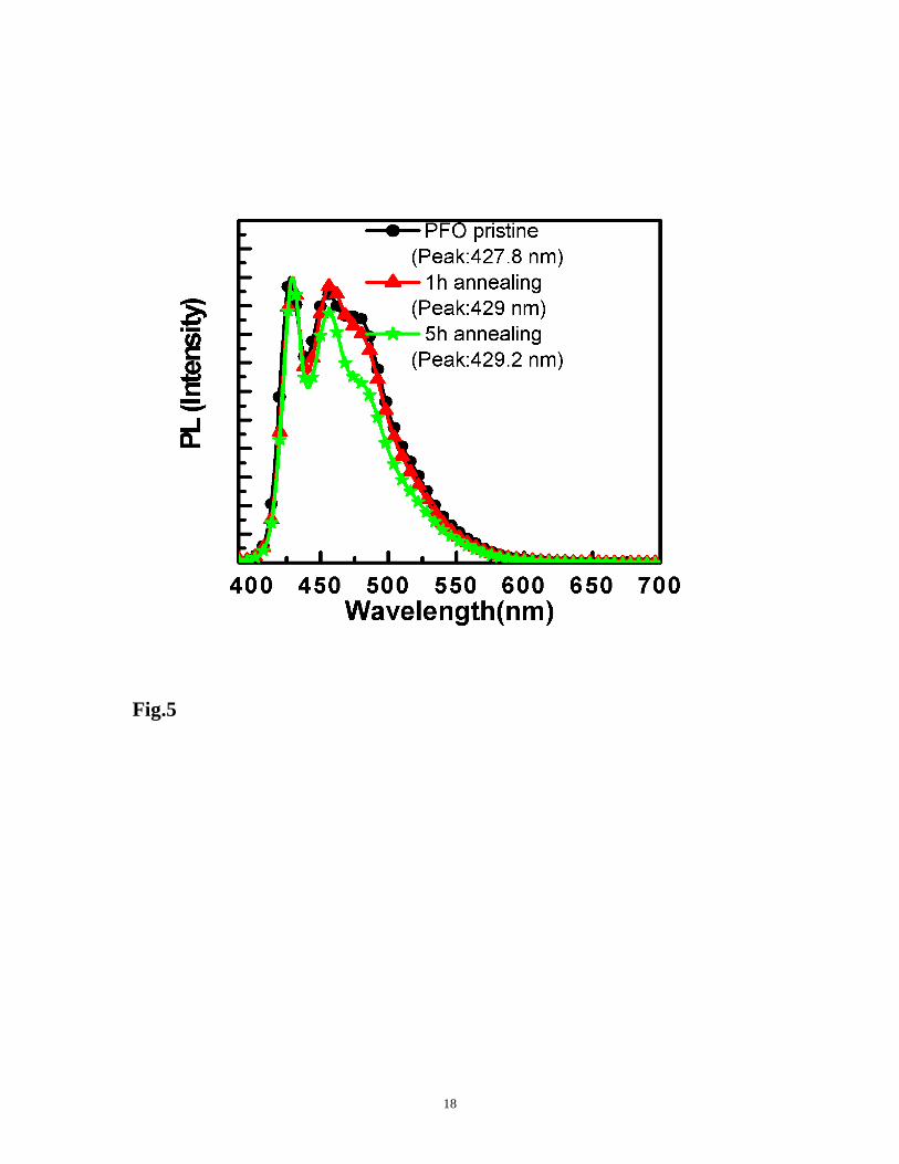
evaporated. It was found that there was some redshift of PL spectra of the vapor
5
annealing devices.(fig.S1). Reorientation of polymer chain might make the polymer film
more orderly so as to introduce redshift of PL spectra, which might be another reason to
increase the efficiency.
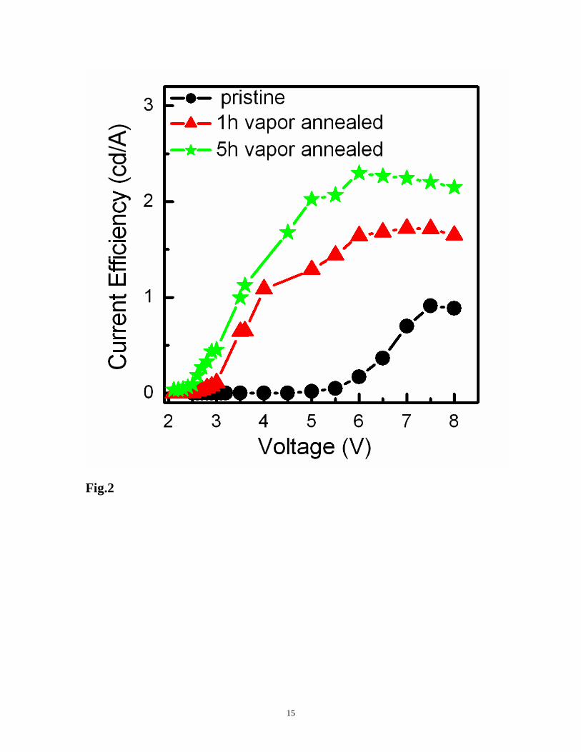
Measurement of the current density-voltage (J–V) (J = I/(device area))
characteristics of OLED devices is the general method used to study various injection and
transport mechanisms in different device configurations. The J–V characteristics of
OLED devices strongly depend on various physical parameters (type of electrodes,
active-layer thickness and structure, applied field, temperature, morphology, etc.) In this
work we focus on the interfacial properties region of the J–V curve, reflecting the
cathode/Al interaction. Electron and hole injections are controlled by the height of the
potential barriers of the interface, ФB, defined by the difference between the work
function of the metal and the highest occupied molecular orbital (HOMO) of the light
emitting polymer, and between the ITO and lowest unoccupied molecular orbital (LUMO)
of the hole transporting layer, respectively.[15,16] If there is a significant difference in
the ФB for the two interfaces, the smaller of the two barriers initially controls the J–V
characteristics, and the larger one controls the J–V characteristics in the EL condition.[17]
In our case, the energy level of HOMO of PFO and PEDOT:PSS are 5.8 eV, 5.2 eV,
respectively. LUMO of PFO is 2.6 eV and the work function of Al is 4.1 eV. The J-V
curves (Figure 3) of the three different devices can be divided into 3 distinct regions of
the applied potential based on the charge transport properties in the PFO layer. Since the
injection barrier between Al and PFO for electrons is larger than that between PEDOT
and PFO for holes. Holes were injected into the emission layer at the initial potentials, it
is region 1. It should be noted that regions 1 doesn’t show associated measurable EL
6
emission because of the low carrier-injection density. As the applied voltage is increased
into region 2 when electrons meet with holes initially, unless an appreciable number of
holes overcome the barrier height between Al and the LUMO of the active layer, no
measurable emission is detected. We therefore focus our attention on region 2 whose
change could reflect the electron-injection at the interface of polymer and cathode since
we modified the surface by vapor annealing. The result shows that light turn-on voltages
of vapor annealed devices are lower than that of the pristine device with the demonstrated
result that the longer the annealing time, the brighter the device at a given voltage. The
increase in brightness is impliedly attributed to the change on the PFO/Al interface due to
the solvent vapor annealing.
We have estimated the reduced energy barrier for electron injection at the cathode
by the Richardson-Schottky (RS) model based on the experimental data. In the reported
devices, the electron injection barrier between PFOEO3 and Al (~1.5 eV) is much higher
than that at the anode for holes (~0.6 eV). Therefore the initial charge inject in region 1 of
Figure 3 is mainly due to hole injection from the anode. We mainly estimated the barriers
using the data from region 2 whose change could reflect the electron-injection at the
interface of polymer and cathode when electrons meet with holes initially. Region 2, the
nonlinear portion of the J-V curve of Figure 3 (insert), is a consequence of the difficulty
of injecting electrons through the junction barrier at the cathode of the device. In region 2
the character of the J–V curve is completely dominated by the barrier potential at the
cathode. When the applied voltage is increased, exceeding the required energy to
overcome the potential barrier, the J–V curve in region 3 is dominated by space charge
limited current with a trapping mechanism. Therefore, the J-V curve characteristic of this
7
device suggests the current is injection-limited in region 1 and 2, but bulk-limited in
region 3. In this case, it is logical to assume that, because of the relatively high barrier
between the Al cathode and the PFOEO3, charge transport is considered to be unipolar.
The steeper regions 2 of 3-5V in the graphs of Figure 3 correspond to the knee in the J–V
characteristics, and this is the region where the electron injection through the polymer/Al
interface barrier takes place. If the applied voltage exceeds the required energy to
overcome the potential barrier, such as 6V, then the J-V characteristic is dominated by
bulk limited mechanism. The decrease in current density in the annealed sample is
implied that charge transport and recombination efficiency of the bulk film are changed
by annealing. (Figure 2) It might due to the enhanced injected electrons role as hole-traps
in the bulk. The vapor annealing effect on bulk film has been under the further study.
The J-V characteristic in region 2 would be continuously influenced by the barrier
potential. Electron injection can occur either by thermionic emission or tunneling in the
situation studied. However, thermionic emission may play some role at room temperature
and the tunneling model does not fit our data very well. Therefore, we focus our attention
on regions 2 where EL emission associated with the carrier injection.[18]
−Φ−=
kT
FeAJ rB επε0
3 4/exp* (Equation 1)
Where BΦ denotes the energy barrier at the metal-polymer interface. F is the
applied electric field (F = V/d where d is the active-layer thickness). T is temperature, k is
the Boltzmann constant. The coefficient A* is experimentally found to be significantly
smaller for organic semiconductors than expected from RS model. We used its room-
temperature value of 1011 Am-2 in the simulation.[19,20]
8
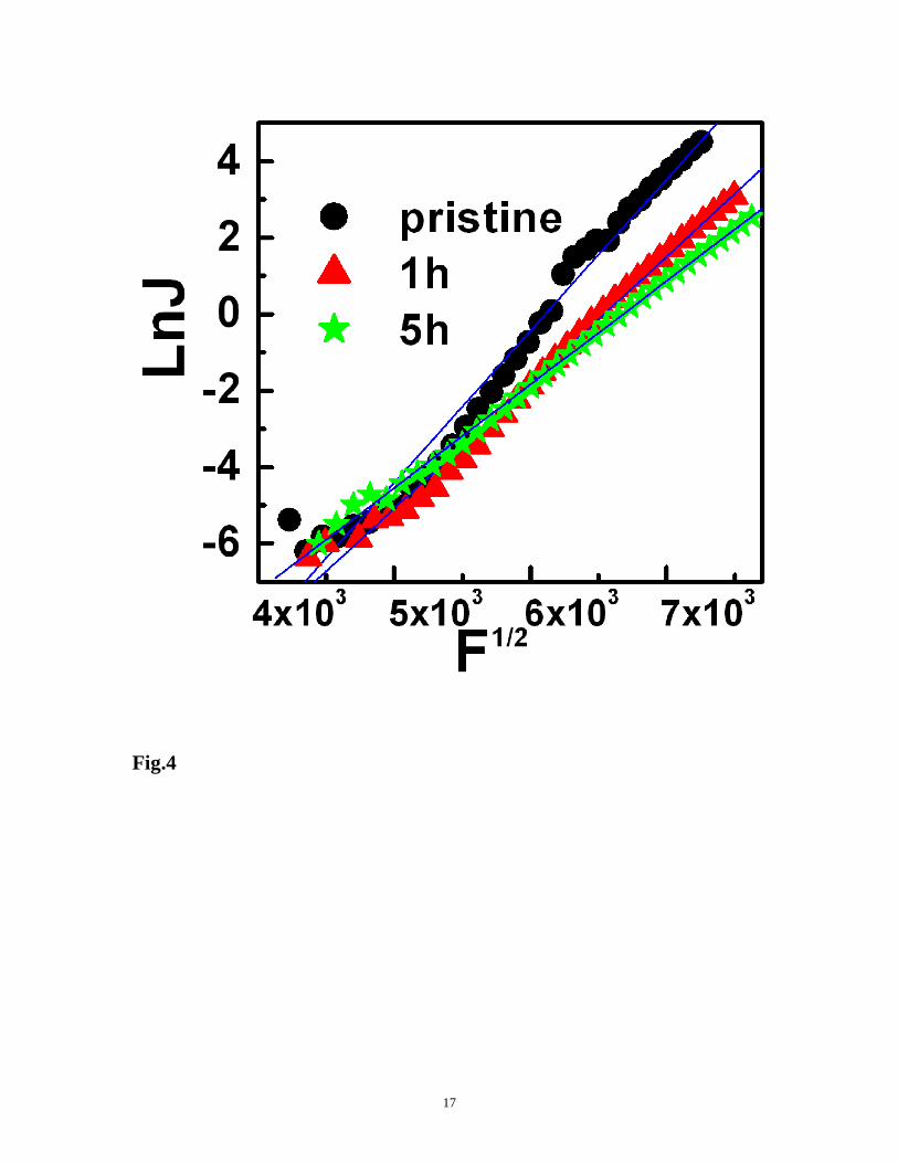
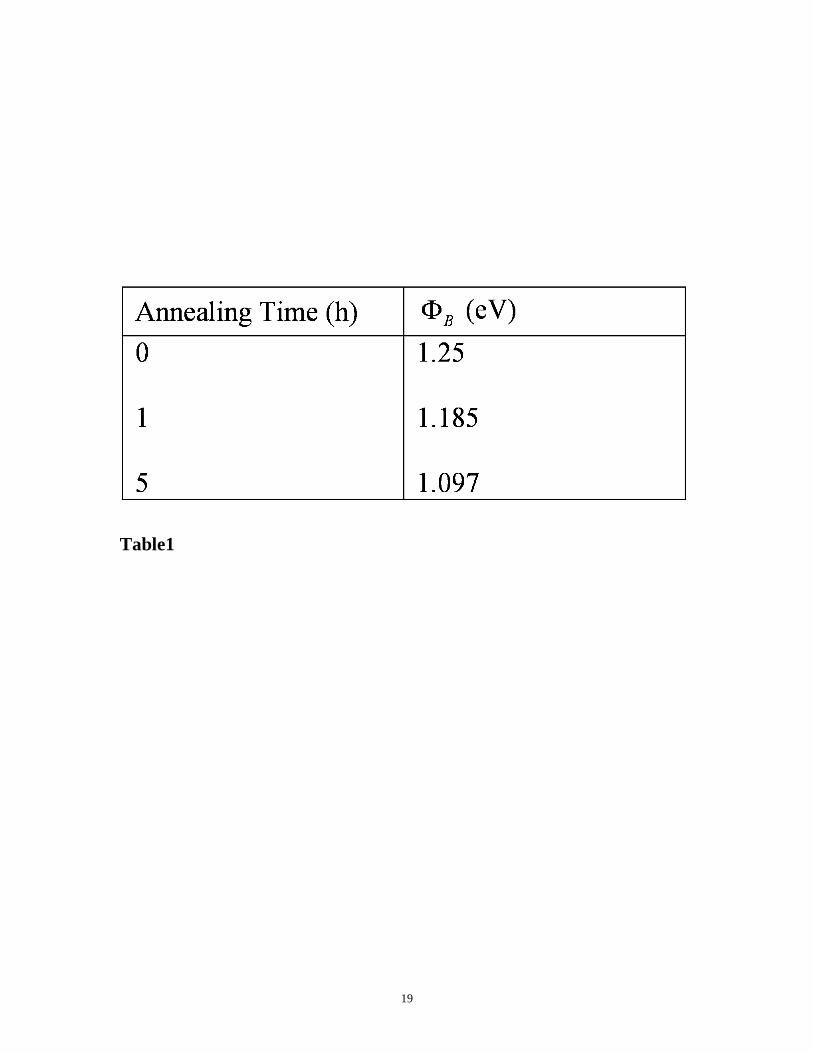
Figure 4 shows a plot of LnJ versus 2/1F with J-V data taken from region 2 for
all 3 types of devices. From the linear fit of the data for each type of device, the barrier
height to electron injection could be obtained. For pristine PFOEO3 device, the RS model
calculation barrier height is 1.25 eV, which is close to the expected value of 1.5 eV
estimated from the difference between Al work function and the LUMO of PFOEO3.
1.185 eV and 1.097 eV were calculation based on the RS model for the devices vapor
annealed for 1 hour and 5 hours respectively. The calculation result also shows solvent
annealing decreases the electron injection barrier.
The effect of annealing the PFOEO3 layer can be explained by the chemical
structure of the polymer as well as the physical interaction between the polymer and the
toluene vapor. Reorientation of polymer chain might make the polymer film more orderly
so as to introduce redshift of PL spectra (Figure.5). And it is also possible that the
reorientation might change interface dipole which induce vacuum level.PFOEO3
consists of two components: the conjugated conductive fluorene backbone (π bond) and
the flexible non-conductive ethyleneoxide side chains (σ bond).[13,21-23] These side
chains do not support charge transport and light emitting characteristics of the polymer
but only provide solubility for solution processing. The conjugated fluorene backbones
are likely to be parallel to the surface due to solution processing, while the side chains
have a more random orientation between each conjugated backbone. Therefore, we could
suppose that there are two components in the “effective barrier height,”φ , of the PFOEO3
and metal contact at the cathode: An intrinsic component, iφ , between the conductive
fluorene backbones and the Al cathode, and an extra component, φ∆ , between the
9
nonconductive side chains and the Al cathode, therefore iφ φ φ= + ∆ . The extra
component is dependent on detailed molecular conformations and local interfacial
morphology. The random orientation of flexible side chains can shield the conjugated
backbones from intimate contacts with Al cathode.[12] When exposed to non-polar
aromatic solvent vapor, there is the tendency for the polar nonconductive side chains to
retreat from the surface to expose the conductive polyfluorene backbone. This
reorientation of the side chains provides an intimate contact between the polyfluorene
backbone and the Al cathode with reduced interference from the side chains reducingφ∆ .
Therefore, the charge barrier between the PFOEO3 and the Al cathode was reduced in the
device with solvent vapor annealing and electron-injection was increased. More balanced
charge injection enhanced the performance of the device.
4. Conclusion
In summary, we have developed an efficient bilayer polymer OLED by solvent
vapor annealing to change the surface morphology of the light emitting polymer. The
change of the light emitting polymer surface morphology dramatically improves the
electron injection from the Al cathode. The solvent annealing could be a practical
approach to significantly improving the polymer based OLED device without change the
chemistry of the material. An efficiency of 2.3 cd/A at 6 V was obtained in a simple
bilayer device configuration with Al cathode. The enhancement of efficiency was
partially attributed to the chain reorientation after solvent vapor treatment which
improved the contact of polymer/metal interface and deduced the electron-injection
barrier. The effect of the barrier reduction has been estimated using the RS model. There
10
is other possible that reorientation of polymer chain change the morphology of the
polymer film, which increase the efficiency.
Acknowledgments
This project is sponsored by the U.S. Department of Energy’s Building
Technologies (BT) Program and the National Energy Technology Laboratory through its
competitive research and development (R&D) program. The goal of the DOE/BT's
Lighting R&D Program is to develop viable technologies having the technical potential to
conserve 50% of lighting consumption by 2025. The Program partners with industry,
utilities, universities, and research institutions to create energy efficient lighting
technologies in pursuit of this goal.
References
[1] Burroughes J H, Bradley D D C, Brown A R, Marks R N, Mackay K, Friend R H,
Burns P L and Holmes A B 1990 Nature 347 539.
[2] Neher D 2001 Macromol. Rapid Commun. 221366.
[3] Campbell A J, Bradley D D C and Antoniadis H 2001 J. Appl. Phys. 89 3343.
[4] Tseng S R, Li S Y, Meng H F, Yu Y H, Yang C M, Liao H H, Horng S F
and Hsu C S 2007 J. Appl. Phys. 101 084510.
[5] Zhou G, Geng Y H, Cheng Y X, Xie Z Y, Wang L X, Jing X B and Wang F S
2006 Appl. Phys. Lett. 89 233501.
[6] Babel A and Jenekhe S A 2003 Macromolecules 36 7759.
11
[7] Prins P, Grozema F C, Nehls B S, Farrell T, Scherf U and Siebbeles L D A
2006 Phys. Rev. B 74 113203.
[8] Campbell A J, Bradley D D C and Antoniadis H 2001 Appl. Phys. Lett. 79 2133.
[9] Yang L, Feng J K, Liao Y and Ren A M 2005 Polymer 46 9955.
[10] Campbell A J, Bradley D D C, Virgili T, Lidzey D G and Antoniadis H 2001 Appl.
Phys. Lett. 79 3872.
[11] List E J W, Guentner R, de Freitas P S and Scherf U 2002 Adv. Mater. 14 374.
[12] Shi Y, Liu J and Yang Y 2000 J. Appl. Phys. 87 4254.
[13] Liu J, Guo T F, Shi Y J and Yang Y 2001 J. Appl. Phys. 89 3668.
[14] Lee T W and Park O O 2000 Adv. Mater. 12 801.
[15] Blom P W M, deJong M J M and Vleggaar J J M 1996 Appl. Phys. Lett. 68
3308.
[16] Davids P S, Campbell I H and Smith D L 1997J. Appl. Phys. 82 6319.
[17] Al Attar H A and Monkman A P 2006 Adv. Funct. Mater. 16 2231.
[18] Barth S., Wolf U, Bassler H, Muller P, Riel H, Vestweber H, Seidler P F and
Riess W 1999 Phys. Rev. B 60 8791.
[19] Arkhipov V I and Bassler H 2000 Appl. Phys. Lett. 77 2758.
[20] Bohnenbuck B, von Hauff E, Parisi J, Deibel C and Dyakonov V 2006 J. Appl.
Phys. 99 024506.
[21] Yu G, Zhang C and Heeger A J 1994 Appl. Phys. Lett. 64 1540.
[22] Malliaras G G, Salem J R, Brock P J and Scott C Phys. 1998 Rev. B 58 13411.
[23] Liu G, Johnson S and Kerr J B 2004 Mat. Res. Soc. Symp. Proc. V6.8.1 796.

12
13
Figure Captions
Figure 1: Brightness vs. voltage characteristics of the devices. Inset shows the molecular
structure of PFOEO3
Figure 2. Current efficiency vs. voltage of the devices
Figure 3. Current density vs. voltage of the devices in a log-log scale. The inset shows
the curve shape on a linear scale
Figure 4. RS plot in region 2 of the devices with various annealing time at room
temperature
Figure 5. Photoluminescence spectra of the films with different annealing time
Table Caption
Table 1. The RS model calculated electron injection barrier heights.
14
Fig.1
15
Fig.2
16
Fig.3
17
Fig.4
18
Fig.5
19
Table1


![Highly Elastic Slide‐Ring Hydrogel with Good Recovery as ...cross-linked polymer network and the high content of solvent,[6] has been widely regarded as a type of highly elastic](https://img.pdfslide.us/doc/110x75/60b853dc9695f018f9482f83/highly-elastic-slidearing-hydrogel-with-good-recovery-as-cross-linked-polymer.jpg)


![using functional highly porous polymer scaffolds to ... · using functional highly porous polymer scaffolds to establish biomimicry of the bone marrow niche. Biomaterials, 225, [119533]](https://img.pdfslide.us/doc/110x75/5f3ec58f9b949b3cfa5bec94/using-functional-highly-porous-polymer-scaffolds-to-using-functional-highly.jpg)