Embed Size (px)
Citation preview
Highly Contrasting Static Charging and Bias Stress Effects inPentacene Transistors with Polystyrene HeterostructuresIncorporating Oxidizable N,N′‑Bis(4-methoxyphenyl)aniline SideChains as Gate DielectricsQingyang Zhang,† Tejaswini S. Kale,†,‡ Evan Plunkett,§ Wei Shi,† B. J. Kirby,∥ Daniel H. Reich,§
and Howard E. Katz*,†,‡
†Department of Materials Science and Engineering, ‡Department of Chemistry, and §Department of Physics and Astronomy, JohnsHopkins University, Baltimore, Maryland 21218, United States∥Center for Neutron Research, National Institute of Standards and Technology, Gaithersburg, Maryland 20899-6102, United States
*S Supporting Information
ABSTRACT: Charge storage and trapping properties ofpolymer dielectrics govern the charge densities of adjacentsemiconductors and greatly influence the on−off switchingvoltage (threshold voltage, Vth) of organic field-effecttransistors (OFETs) when the polymers are used as gateinsulators. Intentional charging of polymer dielectrics inOFETs can change Vth and affect the bias stress. We describea chemical design and fabrication protocol to constructmultilayer-stack dielectrics for pentacene-based OFETs usingdifferent polystyrene (PS)-based polymers in each layer, withoxidizable N,N-bis(4-methoxyphenyl)anilino (TPAOMe)-substituted styrene copolymers in arbitrary vertical positions in thestacks. Thermal, byproduct-free cross-linking of benzocyclobutene subunits provides integrity to the multilayer structure bypreventing dissolution of the previous deposited layer. Neutron reflectivity data verified the multilayer morphology. Wecompared the Vth shift before and after charging the stacks by application of ±100 V across 0.5−1 μm total film thicknesses. Biasstress was the dominant effect in bilayer devices with a TPAOMe layer in contact with the pentacene, indicated by the directionof Vth shift associated with either polarity of external electric field. In structures with no TPAOMe subunit in contact with thepentacene, when charging with −100 V on top of the source and drain electrodes, electron injection from pentacene todielectric was the major charging mechanism, again consistent with the bias stress direction. When charging with +100 V,bilayer devices without TPAOMe showed little change in Vth, suggesting there was no bias stress effect or charge injection inthese devices for this charging polarity. For the bilayer devices with the TPAOMe layer in the bottom, and the trilayer deviceswith TPOMe in the middle, when +100 V was applied, the Vth shifts were opposite those expected from bias stress. Dipoleformation or partial ionization of chargeable groups at the interface between the dielectric layers are likely polarizationmechanisms in these cases. A simple analytical model supports the plausibility of these mechanisms. This work providesexamples of both stabilization and shifting of Vth, and therefore controlling charge carrier density, in semiconductors overlyingthe dielectric multilayers.
■ INTRODUCTION
Electronics based on flexible materials are attractive for use ona wide variety of substrates including foldable, curved, andconforming surfaces for various applications.1,2 Sensing, energyconversion, and memory devices have been made with organicsemiconductors (OSCs) due to their possible transparent,flexible, and printable attributes.3−7 Besides the OSCs,chargeable dielectric polymers that are easy to modify throughmolecular tailoring and can be easily processed in solution areconsidered promising candidates for the fabrication oftransparent, flexible, and nonvolatile organic field-effecttransistor OFET-based components.8−10 More broadly, charge
storage in polymer dielectrics can control the initial chargedensities of OFETs and other semiconductor devices.11,12
Gate dielectric polymers have a great influence on thethreshold voltage (Vth, the gate voltage beyond which on-statemobility is observed) of OFETs because the bulk and interfaceproperties of polymers affect the number densities, energies,and mobilities of charger carriers in the OSCs.13,14 Vth is ameasure of free or trapped charge carrier density in theconductive path through a gated transistor semiconductor.
Received: March 20, 2018Revised: July 17, 2018Published: August 1, 2018
Article
pubs.acs.org/MacromoleculesCite This: Macromolecules 2018, 51, 6011−6020
© 2018 American Chemical Society 6011 DOI: 10.1021/acs.macromol.8b00596Macromolecules 2018, 51, 6011−6020
Dow
nloa
ded
via
NA
TL
IN
ST O
F ST
AN
DA
RD
S &
TE
CH
NO
LO
GY
on
Aug
ust 2
3, 2
019
at 1
9:43
:50
(UT
C).
See
http
s://p
ubs.
acs.
org/
shar
ingg
uide
lines
for
opt
ions
on
how
to le
gitim
atel
y sh
are
publ
ishe
d ar
ticle
s.
Therefore, at a given gate voltage (Vg), the free or trappedcharge carrier density changed by a charging process causes adifferent output current profile and thus a different Vth.Charge trapping is common in dielectric polymers and can
occur within the bulk dielectric or at the interface between thedielectric and organic semiconductor.15 Methods to tune Vthand charge the device include charging of embedded grains ornanostructures and embedding a floating gate sandwichedbetween two dielectric layers.16,17,8 An evaporated Au filmembedded between polysilsesquioxane layers in poly(3-hexylthiophene) (P3HT)-based memory devices showed Vthshift after charging due to the electron transfer from thedepletion region of P3HT to the Au floating gate.18 A ZnOtrap layer sandwiched between methyl silsesquioxane geldielectric layers showed long retention time and low operatingvoltage.19 Another way to modify Vth is to store charge in thebulk dielectric of a chargeable polymer. One example is poly(2-vinylnaphthalene),20 which has quasi-permanent electretchargeability. Another is poly(vinylidene fluoride)(PVDF),21,22 a ferroelectric polymer that has quasi-permanentdipole polarization that changes direction in response to anapplied electrical field. Hydrophobic polymers such as thosebased on polystyrene showed stable Vth shift compared tohydrophilic dielectric polymers.10 The effect of thickness onthe charge trapping of single-poly(N-vinylcarbazole)-gatedielectric pentacene-based OFETs was investigated. Thecharge trapping capacity showed a Gaussian distributionalong the thickness, and the surface tuning distance for chargeinjection showed exponential decrease.23 On the basis of that, asingle continuous dielectric was found to consist of a tunnelinglayer near the channel in addition to the chargeable bulk.The bias stress effect may arise from charge trapping or
detrapping at the interface between the semiconductor andgate dielectric. That results in charges becoming localized andimmobile in the first case or freer to be transported in thesecond case.24−26 In one experiment, delamination of OFETsshowed that charge trapping in a stressed device only occurs inthe gate dielectric.27 Subtle physical and chemical effects at theinterface affect the charge trapping, such as the presence ofbranching and chain ends greatly increasing the bias stresseffect.28,29 A fluorinated gate dielectric, which was highlyhydrophobic and which altered the morphology and adhesionability of the interface, showed the ability to decrease thecharge trapping density at the OSC/dielectric interface, thuslowering the bias stress effect.30 According to the acceptedunderstanding of the bias stress effect as generally applied to p-channel (hole-carrying) OSCs, positive charge trapped in thedielectric interface leads to fewer mobile holes in the channelof the OSC for a given applied gate voltage and thus increasesthe magnitude of Vth.
27,31
We have recently demonstrated9 charge trapping and biasstress effects in pentacene-based OFETs with multilayerdielectrics composed of styrene copolymers. The substituentsin these polystyrene (PS)-based polymers were triphenylamine(TPA) and fullerene (C60). The former is a strong electrondonor often used in OLED devices, and the latter is an electronacceptor. Devices with a bilayer gate dielectric in which asubstituted-PS layer was on top and in contact with thepentacene were found to have a strong charging trapping effectas demonstrated by increased Vth shift. Meanwhile, deviceswith a trilayer gate dielectric were found to have decreased Vthshift, which could possibly be due to the polarization of thesubstituted PS in the middle layer compensating for the
charging trapping or bias stress effects in the top layer. Thispaper established a method to introduce vertically localizedfunctionality in single PS-based polymers and utilize chargedheterostructures in various electronic devices.In this paper, we constructed a series of PS-based multilayer
dielectrics that show even more pronounced charging effects.We introduce a new substituent unit, N,N-bis(4-methoxy-phenyl)anilino (triphenylamine-OMe, TPAOMe), which is astronger electron donor than TPA.32,33 Analogous to what wehad done in previously published work,9 we constructed threetypes of vertical multilayer structures in pentacene bottom gateOFETs with the substituted PS layer in the top, middle, andbottom. 4-Vinylbenzocyclobutene was used as the cross-linkingsubunit to ensure the integrity of the different vertical stacksand prevent any small molecular byproducts.9 No inorganicdielectric was used, and the PS-based polymers were used asthe sole gate dielectric materials. Different charging effectswere observed as Vth shifts from multilayers with differentvertical positions of the PS substituents, including stability tocharging, bias stress, and charging counter to bias stress effects.Vth shifts were more obvious and more precise in the currentwork, and the directions of the shifts were generally consistentwith what would be expected from bias stress. However, in twonew and striking cases, the shifts were opposite fromexpectations based on bias stress, and for those cases,alternative polarizing mechanisms are proposed. A chargedistribution model was correlated to the observed shifts, andeffects of different leakage current levels were evaluated. Thesystems described in this work offer greater systematicmodulation of static charge-induced semiconductor chargedensities than has previously been achieved with polymerelectret gates.
■ EXPERIMENTAL SECTIONSynthesis of PS-Based Polymers. Synthesis of Diarylamine 3.
An oven-dried round-bottom flask was evacuated and backfilled withnitrogen to maintain inert atmosphere. Pd2(dba)3 (dba =dibenzylideneacetone, 25 mg, 0.03 mmol) and P(tBu)3HBF4 (16mg, 0.05 mmol) were added to this flask, and the flask was placedunder vacuum for 10 min. Then, p-methoxyaniline (0.5 g, 4 mmol), p-bromoanisole (0.5 g, 2.7 mmol), and sodium tert-butoxide (0.4 g, 4mmol) were added under the flow of nitrogen gas, and the flask wasplaced under vacuum for 30 min, following which it was filled withnitrogen gas. 30 mL of freshly degassed, dry toluene was added via acannula, and the reaction vessel was placed in a preheated oil bath at105 °C. The reaction was continued under nitrogen for 10 h. Aftercompletion of the reaction, the reaction mixture was cooled to roomtemperature and filtered over Celite. Toluene was removed in vacuo.To the resultant slurry, 50 mL of deionized (DI) water was added,and the product was extracted into ethyl acetate. The product waspurified using column chromatography using hexanes/ethyl acetate toobtain the product as an off-white solid. This was recrystallized fromhexanes to obtain the pure product as needlelike crystals (0.43 g, 1.9mmol, 70%). The 1H NMR of the product was found to agree withprevious literature.34
Synthesis of Triarylamine 6. An oven-dried round-bottom flaskwas evacuated and backfilled with nitrogen to maintain inertatmosphere. Pd2(dba)3 (18 mg, 0.02 mmol) and P(tBu)3HBF4 (12mg, 0.04 mmol) were added to this flask, and the flask was placedunder vacuum for 10 min. Then, 3 (0.45 g, 2 mmol), 535 (0.8 g, 2.1mmol), and sodium tert-butoxide (0.2 g, 2.1 mmol) were added underthe flow of nitrogen gas. The flask was placed under vacuum for 30min, following which it was filled with nitrogen gas. 40 mL of freshlydegassed, dry toluene was added via a cannula, and the reaction vesselwas placed in a preheated oil bath at 105 °C. The reaction wascontinued under nitrogen for 3 h. After completion of reaction, the
Macromolecules Article
DOI: 10.1021/acs.macromol.8b00596Macromolecules 2018, 51, 6011−6020
6012

reaction mixture was cooled to room temperature and filtered overCelite. Toluene was removed in vacuo. To the resultant slurry, 50 mLof DI water was added, and the product was extracted into ethylacetate. The product was purified using column chromatographyusing hexanes/ethyl acetate to obtain the product as a pale yellow oil(0.47 g, 0.9 mmol, 46%).Synthesis of Triarylamine 7. In an oven-dried round-bottom flask,
6 (0.47 g, 0.9 mmol) was dissolved in 20 mL of freshly degassed, dryTHF. To this solution, a 1.0 M solution of tetrabutylammoniumfluoride (1.35 mL, 1.35 mmol) was added, and the reaction wasperformed at room temperature under nitrogen for 10 h. After
completion of reaction, the solvent was removed in vacuo to obtainthe pure product as an off-white solid (0.35 g, 0.9 mmol, 99%).
Synthesis of XLPS 8, PS-10% Cl 9, and XL-PS-10% Cl 10. Thecross-linkable polymer (XLPS) and the precursor polymers (PS-10%Cl and XLPS-10% Cl) were synthesized using the protocols describedin our previously published work.9
Synthesis of PS-10% TPAOMe 11 and XLPS-10% TPAOMe 12. 0.3g of 10% XLPS or XLPS-10% Cl was dissolved into 10 mL ofdehydrated THF, and then 4-hydroxyphenyl-TPAOMe (198.6 mg,0.5 mmol), K2CO3 (69 mg, 0.5 mmol), KI (41.5 mg, 0.25 mmol), andthe cyclic polyether K+ complexing agent 18-crown-6 (13.2 mg, 0.05
Scheme 1. Synthesis of N,N-Bis(4-methoxyphenyl)-4-(4-hydroxyphenyl)aniline (7)
Scheme 2. Synthesis of PS-Based Polymer Dielectric with Cross-Linkable and Chargeable Subunits
Scheme 3. Fabrication Protocol for Pentacene-Based OFETs with PS-Based Polymers as Sole Gate Dielectric Materialsa
aThere are eight OFET devices per 1 in. square Si/SiO2 substrate.
Macromolecules Article
DOI: 10.1021/acs.macromol.8b00596Macromolecules 2018, 51, 6011−6020
6013

mmol) were added swiftly to avoid excess moisture inside. Thereaction mixture was then sealed and heated at reflux under nitrogenat 70 °C for 24 h. After cooling to room temperature, the mixture waspoured into water (200 mL) and then filtered. The filtrate was washedwith water and methanol three times, and the residue was redissolvedin THF and precipitated in methanol (150 mL). The purificationprocedure was repeated three times, and the final polymer was driedunder vacuum overnight, yielding 66% of the desired productpolymer.Device Fabrication and Imaging. Substrate Preparation and
Gate Deposition. The steps used for making test devices areillustrated in Scheme 3. Silicon wafers with 300 nm silicon oxide(used only for its inertness and flatness) deposited on top were dicedinto 1 in. squares and then soaked in 3:1 concentrated H2SO4:30%H2O2 for 30 min (caution: highly corrosive!) followed by sonicating inwater, acetone, and isopropyl alcohol for 15 min each. The substrateswere then dried in nitrogen flow, and chromium/gold (5 nm/35 nm)was then thermally evaporated through a mask to give eight gate padsper wafer.Gate Dielectric Deposition. Multilayers of substituted polystyrene
dielectric were spin-coated over the entire substrate under a drynitrogen atmosphere in a glovebox. All spin-coating solutions wereprepared by dissolving the polymers in chloroform, sonicating at 30°C for 60 min, and filtering into a second vial through a 0.45 μmhydrophobic PTFE syringe filter. The solution was spin-coated with aspeed of 1500 rpm (25 Hz) for 60 s, and the film thickness was variedby using different solution concentrations ranging from 20 to 40 mg/mL.9 To ensure an intact multilayer structure, cross-linking of the XL-PS polymer was done in a vacuum oven at 180 °C under 70−80mmHg for 1.5 h. For all other plain or substituted polystyrenes, thefilm was annealed in the same vacuum oven at 50 °C under 70−80mm for 30 min.Pentacene Semiconductor and Source-Drain Gold Electrode
Deposition. The 50 nm pentacene was thermally evaporated via asubstrate mask to give eight panels aligned over the chromium/goldgate pads electrodes. Following the deposition of pentacene, goldelectrodes were thermally evaporated onto the pentacene through ashadow mask over the gate panels to give 6 mm length and 1.25 mmwidth source-drain pair channels.Scanning Electron Microscope (SEM) Cross-Section Imaging. An
XLPS/XLPS-TPAOMe/PS trilayer device with spin-coating solutionconcentrations of 35, 30, and 30 mg/mL and XLPS/PS bilayerdevices with spin-coating solution concentrations of 40 and 20 mg/mL fabricated using the procedure described above were fracturedusing a diamond scribe to expose their cross sections. The crosssections were sputtered with platinum before imaging. Images wereobtained using a JEOL 6700F SEM.Neutron Reflectivity. Fabrication of Samples for Neutron
Reflectivity. Thermal oxide was completely removed from 38 mm ×38 mm silicon wafers in 6:1 buffered hydrofluoric acid solution.Substrates were then cleaned, and bilayer polymer stacks werefabricated using the procedures described for “gate dielectricdeposition” above. The polymer layers were deposited by spin-coating from 10 mg/mL solutions.Neutron Reflectivity Measurements. Neutron reflectivity measure-
ments were performed on the polarized beam reflectometer (PBR) atthe NIST Center for Neutron Research. The beam consisted of 4.75Å neutrons, as selected with a vertically focusing pyrolytic graphitemonochromator. Borated aluminum masks were used to restrict thevertical extent of the beam to a 30 mm tall region in the center of thesample. Specular reflectivity measurements were performed in therange 0.2° < 2θ < 4.4°, where 2θ is the scattering angle, whichcorresponds to a wave vector transfer Q perpendicular to the substratespanning 0.005 Å−1 < Q < 0.1 Å−1. Background measurements weretaken in the same range of 2θ with the sample angle offset from thespecular condition by 0.3°.The range of measurement was divided into three configurations of
the four vertical slits that define the PBR’s beam divergence. For Q <0.045 Å−1 slits of width 0.5, 0.5, 1, and 1 mm were used; the range0.035 Å−1 < Q < 0.7 Å−1 was measured using slits of 0.7, 0.7, 1.2, and
1.2 mm, and the range Q > 0.06 Å−1 was measured using slits of 1.5,1.5, 1.5, and 2 mm. For each sample, data from all threeconfigurations were fit simultaneously to the same theoretical model(see below).
■ RESULTS
In this work, we introduce polystyrenes substituted with thechargeable TPAOMe group, which is a stronger electron donorthan the TPA used in our previous published work.9 10 mol %TPAOMe was introduced after polymerization through theside-chain reaction with 4-vinylbenzyl chloride precursor. The10% concentration was found to balance the trade-off betweengood polymer solubility, leading to smooth spincast films andhigh enough donor concentration to be electronicallyinfluential.The work presented here includes several procedural
improvements. More concentrated polymer solutions wereused to spin-coat the dielectric layers, and a mild annealingstep was added after spin-coating. The more robust polymerfilms that resulted allowed higher charging voltages to beapplied and showed reduced gate current leakage and lowerprobabilities of device short circuits compared to the previouspublished work.9 Furthermore, the charging process was doneusing the same system as for I−V testing, reducing the chancesof devices being altered or destroyed by multiple probing. Thegate-semiconductor current was monitored during charging,verifying the stability of the dielectric barriers during thisprocess.Cross-sectional images of the PS polymer dielectric and the
thicknesses of the layers were obtained by SEM. As shown inFigure 1a for a XLPS/XLPS-TPAOMe/PS trilayer (bottom-to-top layer structures are given as left/right or left/middle/rightin text) and in Figure 1b for a XLPS/PS bilayer, distinctdielectric layers were visible due to their differing brightness inthe SEM images. Sharp focus was not obtained due to therough cross section and charging of the dielectric films fromthe electron beam. These results verified that the deposition ofthe second or third layer onto the previously deposited andcross-linked layer(s) did not destroy the integrity of thedielectrics.Figure 2 shows the measured neutron reflectivity for two
bilayer films. The films were identically prepared with bottomlayers of cross-linkable polystyrene with 10% TPAOMe(XLPS-TPAOMe) and a top layer of perdeuterated poly-styrene (d8-PS). The deuteration provided scattering contrastbetween the two organic layers. The data from the three slitconfigurations have been rescaled to show continuousreflectivity profiles.Neutron reflectivity can be used to generate a depth profile
of the nuclear composition of thin films.36 This profileincorporates information about the thickness and chemicalcomposition of each layer as well as the interfacial roughnessesbetween the layers. Information about the composition is inthe form of the scattering length density (SLD) ρ. Theinterfacial roughnesses are modeled as a series of thin layerswith infinitely sharp boundaries whose SLD is interpolatedbetween the two adjacent layers by an error function of the
formσ
−( )erf z z2
i
i, where zi is the location of the layer boundary
determined by the layer thicknesses and σi is the layerroughness reported. The SLD profile ρ(z) can then be used togenerate a theoretical reflectivity profile which can becompared to the measured profile and refined using nonlinear
Macromolecules Article
DOI: 10.1021/acs.macromol.8b00596Macromolecules 2018, 51, 6011−6020
6014

χ2 minimization. This modeling was performed using the Refl1D software package.37 The resulting SLD profiles from thisprocedure are shown in the inset of Figure 2, and thecorresponding reflectivity profiles are plotted with theirrespective experimental data in Figure 2.These results show that spin-coated layers formed from
cross-linkable polystyrenes modified with the TPAOMe grouphave thicknesses consistent with those obtained previously for
unsubstituted and TPA-substituted cross-linkable polystyr-enes.9 The mean interfacial roughness at the XLPS-TPAOMe/d8-PS interface for the two samples measured was 4.86 ± 0.02nm. This was 5.5% of the total layer thickness, demonstratingthe integrity of the copolymer during the cross-linking process.However, the significant increase in interfacial roughness whencompared to the value of ∼2.5 nm found previously for TPA-substituted polystyrenes9 is consistent with the effects of anincrease in free volume and steric hindrance of the TPAOMefunctional group compared with the smaller TPA moiety.The charge trapping properties of the PS-substituted
dielectric films were investigated by measuring the thresholdvoltage shift (ΔVth) before and after charging by observing thetransfer characteristics of OFETs. In this paper, we denote anegative sign of ΔVth as representing a more negative Vgrequired for the OFET to reach the “on” state (“more difficultto turn on”), while a positive sign of ΔVth represents a lessnegative voltage required to reach the “on” state (“easier toturn on”). The transfer curves were obtained by measuringdrain current with Vg increasing from +10 to −70 V, and thedrain-source bias fixed at −70 V. Vth was determined as the x-intercept of a linear fit to the square root transfer curve in theVg range where it is approximately linear.13 We compared Vthbefore and after charging and calculated ΔVth by subtractingthe Vth before charging from Vth measured immediately aftercharging. The voltage we used to charge was Vchg = +100 or−100 V applied simultaneously to the source and drainelectrodes with the gate electrode grounded. This ensuredsufficient stored and trapped charges.I−V measurements on the devices were performed within
4−5 h after fabrication. Charging time for each device was 5min, and the measurement (transfer and output) required 1−2min, so the testing time for each device was 11−15 min.We measured charge trapping and Vth shifts in pentacene
OFET devices with four different dielectric compositions. Thecompositions of the dielectrics and the spin-coating concen-tration of each dielectric layer for each kind of device arepresented in Table 1. The transfer curves of the four different
devices before and after charging at Vchg ± 100 V as well asschematics of each device structure are illustrated in Figure 3.In general, higher spin-coating concentration (30−40 mg/mL,compared to 20 mg/mL used in our previous work) morereliably prevented short circuits or current leakage.Leakage currents varied considerably from device to device,
as discussed later, but were typically within an order ofmagnitude of 0.1 μA for 50 V applied to the gate, for aresistance of 500 MΩ. The specific capacitance for 500 nmthick polystyrene is about 10 nF/cm2, and the device area isabout 0.5 cm2, so gate capacitance for each device is about 5nF. Thus, the RC time constant is on the order of seconds. Thecharging time is 2 orders of magnitude larger. The lowest-
Figure 1. Cross-section SEM images of representative polymerheterostructures. (a) XLPS/XLPS-TPAOMe/PS trilayer device and(b) XLPS/PS bilayer device. Film deposited on the silicon/siliconoxide substrate. For the trilayer, the thickness of each layer top downwas 320 ± 12 nm, 300 ± 13 nm, and 300 ± 16.0 nm. For the bilayer,the thickness of each layer top down was 170 ± 8 nm and 300 ± 20nm. The determination of thickness was based on 10 measurementsof each layer with uncertainties expressed as one standard deviation.
Figure 2. Measured reflectivity for two bilayer films of spin-coatedXLPS-TPAOMe/d8-PS. The upper set of data has been offset by afactor of 10 for clarity. The solid lines through the data are best-fitmodel curves determined from analysis described in the text. Thismodeling yielded the scattering length density (SLD) profiles shownin the insets with interfacial roughnesses at the XLPS-TPAOMe/d8-PS interface of 4.81 ± 0.02 nm and 4.92 ± 0.03 nm for film 1 and film2, respectively. The zero of the depth axis is the top of the underlyingSi wafer. Error bars on the data and fitting parameters correspond to±1 standard deviation.
Table 1. Dielectric Layer Structure and Spin-CoatingConcentration of the Four Different Device ConfigurationsShown in Figure 3
dielectric composition(bottom-to-top)
spin-coating concentration(mg/mL)
XLPS/PS 40/20XLPS/TPAOMe 40/30XLPS/XLPS-TPAOMe/PS 35/30/30XLPS-TPAOMe/PS 40/30
Macromolecules Article
DOI: 10.1021/acs.macromol.8b00596Macromolecules 2018, 51, 6011−6020
6015

leakage-current devices could have RC time constants on thesame order as the charging time. Recording a transfer curvealso takes seconds and involves only transient application ofgate voltage equal to the charging voltage. Thus, chargingeffectiveness should be relatively independent of RC timeconstraints, and there should be minimal discharging duringmost of the transfer curve recording procedure.Transfer curves from multiple devices with each dielectric
configuration and each charging polarity were obtained beforeand immediately after charging, and Vth shifts were calculated.A compilation of the Vth shifts for all the devices measured isshown in Figure 4, together with means and ranges for eachsample configuration/charging polarity pair. For the bilayerstructure with no substituent (XLPS/PS), steady and largepositive Vth shifts were observed when applying Vchg = −100 Vto the source and drain electrodes during charging. Whenapplying Vchg = +100 V, inconsistent and negligible Vth shiftswere observed.Again referring to Figure 4, Vth shifts in the directions that
would result from bias stress effects were seen in bilayerstructures with a 10% TPAOMe-substituted layer on top of the
cross-linked PS layer (XLPS/PS-TPAOMe). We observed aconsistent positive Vth shift when Vchg = −100 V was applied
Figure 3. (a, d, g, j) Schematics of the pentacene OFET device architectures studied. (b, e, h, k) Representative transfer curves for correspondingpentacene OFET devices before and after charging at Vchg = −100 V. (c, f, i, l) Transfer curves for four different corresponding pentacene OFETdevices before and after charging at Vchg = +100 V.
Figure 4. A boxplot of the threshold voltage shifts ΔVth as a resultcharging with Vchg = ±100 V. We denote negative shift as an increasein the magnitude of the Vth, indicating devices were harder to turn onand a positive shift as a decrease in the magnitude of the Vth. From leftto right: Vth shift for XLPS/PS-TPAOMe, XLPS/PS, XLPS-TPAOMe/PS, and PS/XLPS-TPAOMe/XLPS.
Macromolecules Article
DOI: 10.1021/acs.macromol.8b00596Macromolecules 2018, 51, 6011−6020
6016

on top and a consistent negative Vth shift when Vchg = +100 Vwas applied. The data indicate that the substituted layer nearthe OSC/dielectric interface responded to the applied electricfield to trap or free charge carriers in the adjacent pentacenelayer, which is consistent with the theory of bias stress effects.26
For the trilayer structure (XLPS/PS-TPAOMe/PS), largenegative threshold voltage shifts, which made the devices mucheasier to turn on, were observed when both signs of voltages wereapplied. The situation was very different from the unsubstitutedbilayer structure because Vchg = +100 V resulted in large Vthshifts in the same direction as that resulting from Vchg = −100V, while there was no obvious Vth shift in the unsubstitutedbilayer structures in the case of Vchg = +100 V. In the chargingof the last bilayer structure (XLPS-TPAOMe/PS), somewhatsmaller Vth shifts were observed when both signs of Vchg wereapplied. The direction of shifts was the same as that of thetrilayer structure and again independent of the sign of Vchg.
■ DISCUSSION
In our previous study of the pentacene-based OFETs with PS-based multilayer dielectrics, neutron reflectivity experimentsshowed that spin-coating cross-linkable, chemically similar,hydrophobic polymer solutions created multilayer dielectricstructures with distinct boundaries between the layers.9 TheSEM and neutron reflectivity measurements in this presentstudy show that this approach can be extended to PS-basedpolymers with the larger TPAOMe functional group on sidechains to the PS backbone in any vertical position in themultilayers. Furthermore, the previous study indicated therewas no obvious structure change during the charging ofsubstituted PS-based multilayer pentacene OFET devices,again from neutron reflectivity experiments. Therefore, weshould also be able to exclude structural change-induced effectsin the charging mechanism in this study.For many of the combinations of layers portrayed in Figure
4, we obtained at least two devices with gate leakage currents 2orders of magnitude less than the on currents. The Vth shiftsfor these devices were well within the ranges shown in Figure 4for the sets of devices that included the full leakage currentrange. We assembled a series of square-root and log transfercurves from pairs of devices with a particular architecture,included in the Supporting Information. One member of eachpair (the upper set of curves for each sample) has relatively lowoff current and/or off-current change after charging, while theother (the lower set of curves for each sample) has relativelyhigh off current magnitude and/or change. For each pair, we
see that the Vth shifts are comparable and in the rangesdepicted in Figure 4. Thus, we have experimental evidence thatwhile the charging process may cause some change in chargeinjection or breakdown properties of the gate dielectrics, thestatic charge distribution, responsible for the Vth shifts, is notgreatly sensitive to this aspect of the charging process.Furthermore, previous investigators have presented both
theoretical and experimental38−41 findings regarding a devicemodification leading to changed gate leakage current and theaccompanying Vth shift. In all these cases, the Vth shifts are verysmall (1−5%) compared to the Vg range being swept. All ofour Vth shifts (excluding the one that we consider negligible)are at least 10% of the Vg range, and for the three architecturesthat showed the most substantial Vth shifts, the magnitudes ofthose were much higher than that. A numerical model of theeffect of various magnitudes of gate dielectric resistance(leakage current) on the determination of Vth is presented intext accompanying Figure S12. Our leakage current levels arewell within the range in which our Vth shifts would benegligibly affected.For bilayer structures with substituted chargeable layer (PS-
TPAOMe) on top and in direct contact with the semi-conductor, Vth shifts in the directions that would result frombias stress effects were observed. When positive bias wasapplied on top (same effect as negative gate voltage applied onthe gate), free charge carriers (holes in pentacene) weretrapped and became immobile near the interface, reducing thedrain current and thus the threshold voltage (Figure 5a). Thiseffect was not observed for the bilayer devices withoutTPAOMe. When negative bias was applied to the TPAOMe-on-top bilayer, a positive Vth shift was observed instead,indicating that immobile charge carriers were released andbecame free as electrons were injected into the dielectric(Figure 5b).For all the devices with XLPS or PS on top, electron
injection from semiconductor to dielectric was again thedominating effect when Vchg = −100 V was applied, resulting ina large positive Vth shift (Figure 5b). On the contrary, the largepositive Vth shift observed in the positive charging case for thetrilayer and the XLPS-TPAOMe/PS bilayer devices indicated adifferent mechanism of device polarization. A possibleexplanation was that the TPAOMe layer was polarized toform dipoles responding to the applied electric field or evenbecame partially ionized (Figure 5c). The accumulatingnegative ends of the dipoles or ions presented at the topparts of the interface could have induced free holes in the
Figure 5. Schematic representations of three charging mechanism: (a) OSC/dielectric bias stress effect, (b) electron injection from the source anddrain through the semiconductor, (c) hole injection from the source and drain through the semiconductor, and (d) dielectric polarization or partialionization within the dielectric or at interfaces.
Macromolecules Article
DOI: 10.1021/acs.macromol.8b00596Macromolecules 2018, 51, 6011−6020
6017
pentacene. Charging effects in the trilayer were generally largerthan for the XLPS-TPAOMe/PS bilayer devices. A possiblereason was that in the trilayer case the bottom cross-linkedlayer and the top PS both served to stabilize the stored chargesby blocking their dissipation into either the pentacene OSC orthe gold gate electrode. This mechanism would also beconsistent with charges stored in the bulk, rather than at theouter interfaces, of the trilayer. This observation of largeraverage Vth shifts from the trilayers supports the hypothesisthat the TPAOMe groups do play a role in hosting andstabilizing the static charges and help define the distancesbetween average planes of mutually compensating holes andelectrons in the dielectrics. While we hypothesize that ionizedTPAOMe groups are sites of stored positive charge, thestructural irregularity and free volume associated with thisgroup could also lead to increased sites where charge could betrapped.As an order-of-magnitude estimate of a reasonable quantity
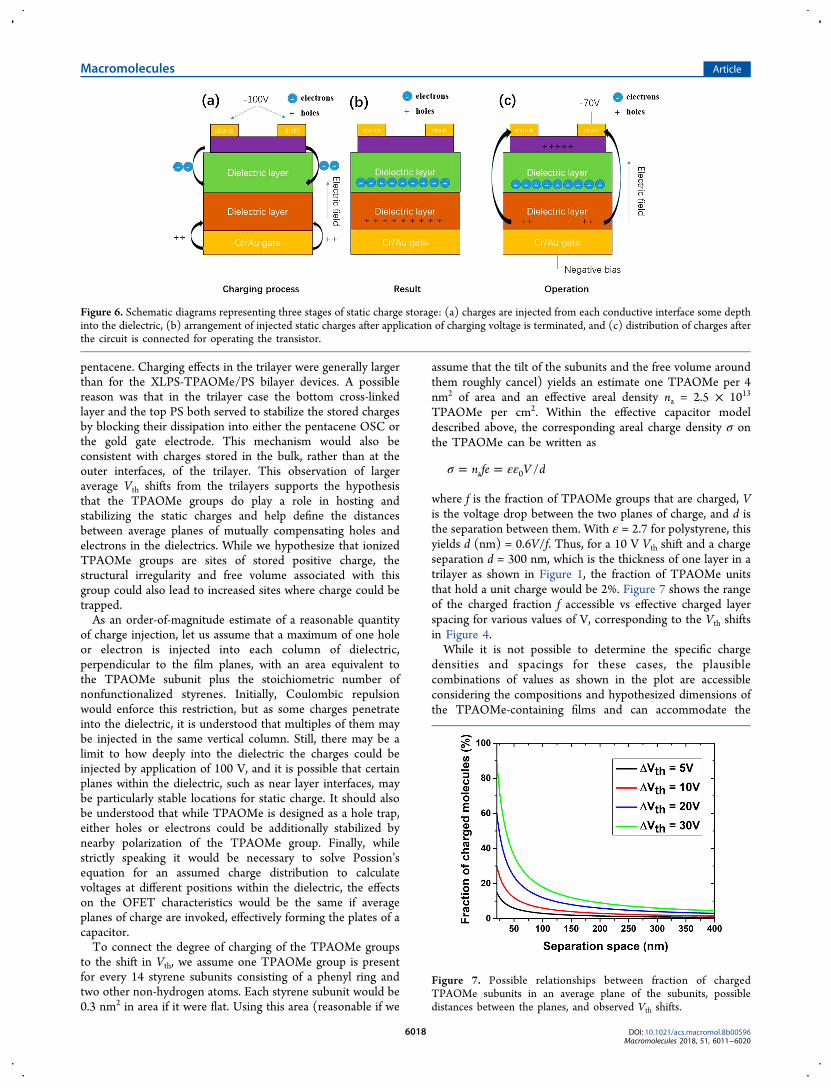
of charge injection, let us assume that a maximum of one holeor electron is injected into each column of dielectric,perpendicular to the film planes, with an area equivalent tothe TPAOMe subunit plus the stoichiometric number ofnonfunctionalized styrenes. Initially, Coulombic repulsionwould enforce this restriction, but as some charges penetrateinto the dielectric, it is understood that multiples of them maybe injected in the same vertical column. Still, there may be alimit to how deeply into the dielectric the charges could beinjected by application of 100 V, and it is possible that certainplanes within the dielectric, such as near layer interfaces, maybe particularly stable locations for static charge. It should alsobe understood that while TPAOMe is designed as a hole trap,either holes or electrons could be additionally stabilized bynearby polarization of the TPAOMe group. Finally, whilestrictly speaking it would be necessary to solve Possion’sequation for an assumed charge distribution to calculatevoltages at different positions within the dielectric, the effectson the OFET characteristics would be the same if averageplanes of charge are invoked, effectively forming the plates of acapacitor.To connect the degree of charging of the TPAOMe groups
to the shift in Vth, we assume one TPAOMe group is presentfor every 14 styrene subunits consisting of a phenyl ring andtwo other non-hydrogen atoms. Each styrene subunit would be0.3 nm2 in area if it were flat. Using this area (reasonable if we
assume that the tilt of the subunits and the free volume aroundthem roughly cancel) yields an estimate one TPAOMe per 4nm2 of area and an effective areal density na = 2.5 × 10¹³
TPAOMe per cm2. Within the effective capacitor modeldescribed above, the corresponding areal charge density σ onthe TPAOMe can be written as
σ εε= =n fe V d/a 0
where f is the fraction of TPAOMe groups that are charged, Vis the voltage drop between the two planes of charge, and d isthe separation between them. With ε = 2.7 for polystyrene, thisyields d (nm) = 0.6V/f. Thus, for a 10 V Vth shift and a chargeseparation d = 300 nm, which is the thickness of one layer in atrilayer as shown in Figure 1, the fraction of TPAOMe unitsthat hold a unit charge would be 2%. Figure 7 shows the rangeof the charged fraction f accessible vs effective charged layerspacing for various values of V, corresponding to the Vth shiftsin Figure 4.While it is not possible to determine the specific charge
densities and spacings for these cases, the plausiblecombinations of values as shown in the plot are accessibleconsidering the compositions and hypothesized dimensions ofthe TPAOMe-containing films and can accommodate the
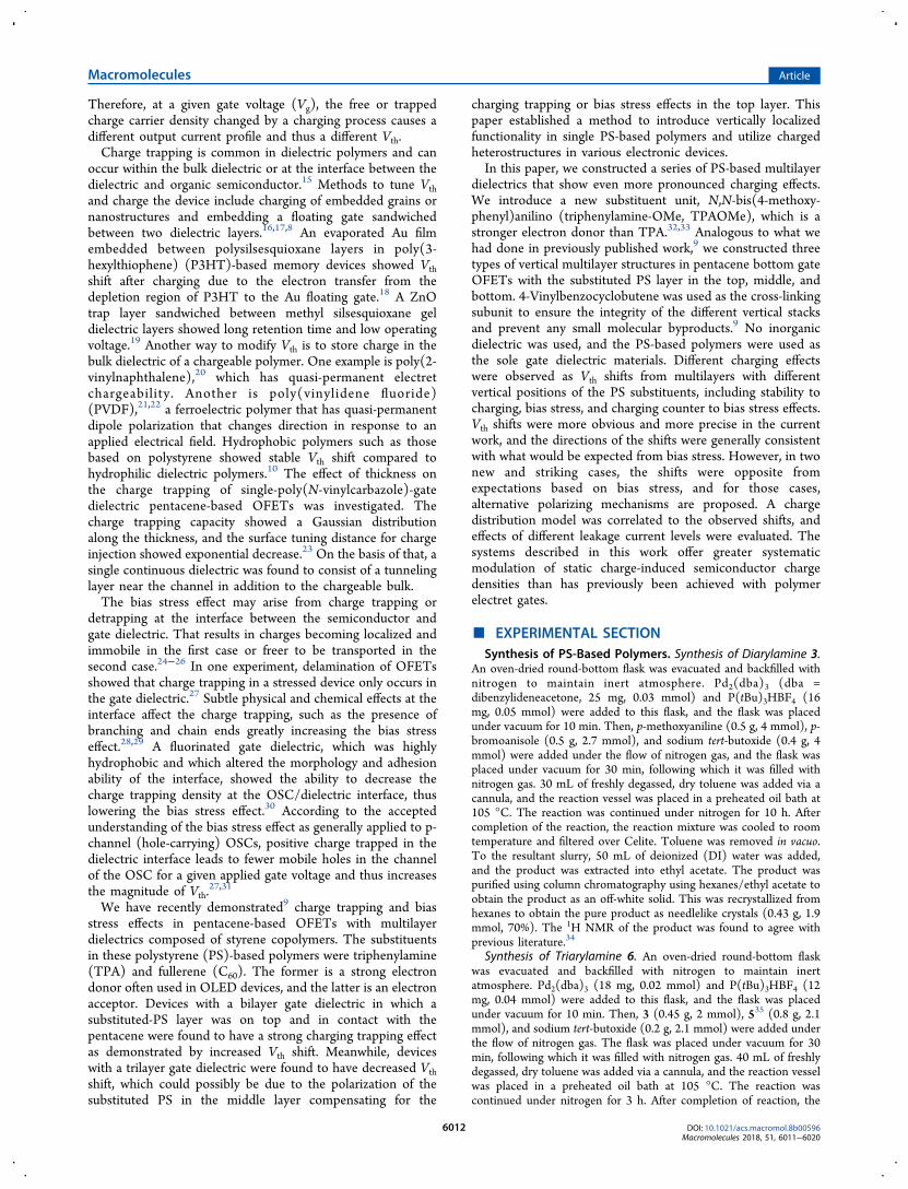
Figure 6. Schematic diagrams representing three stages of static charge storage: (a) charges are injected from each conductive interface some depthinto the dielectric, (b) arrangement of injected static charges after application of charging voltage is terminated, and (c) distribution of charges afterthe circuit is connected for operating the transistor.
Figure 7. Possible relationships between fraction of chargedTPAOMe subunits in an average plane of the subunits, possibledistances between the planes, and observed Vth shifts.
Macromolecules Article
DOI: 10.1021/acs.macromol.8b00596Macromolecules 2018, 51, 6011−6020
6018

interfacial and the charge-separated schemes shown in Figure5.An interesting trend is displayed by all of the Vchg = +100 V
data taken together. Vth shifts progress from more negative tomore positive with TPAOMe on top, absent, on the bottom,and in the middle. This trend is consistent with TPAOMeimposing additional negative Vth by trapping positive charge.This makes the device more difficult to turn on when at thepentacene interface but easier to turn on when remote from it,while the effect is largest with the TPAOMe flanked byunsubstituted PS barriers. The “more negative” Vth effect ofTPAOMe is also observed for the TPAOMe on top relative tothe unsubstituted PS on top with Vchg = −100 V charging, butthe increased charge density in pentacene induced by negativecharging appears to saturate and is not significantly higher withTPAOMe added in layers remote from the pentacene.
■ CONCLUSIONWe synthesized a series of cross-linkable and chargeable PS-based dielectric polymers with 10% benzocyclobutene and 10%TPAOMe function groups. Using these polymers as the solegate dielectric, we constructed three different types ofmultilayer stack dielectrics for pentacene- based OFET devices,with the TPAOMe-substituted chargeable layer either incontact with the pentacene, in contact with the gate, orsandwiched between PS layers without TPAOMe. Thermalcross-linking the benzocyclobutene subunits ensured successfulsuccessive deposition of the polymer layers via spin coating.We compared the Vth shift before and after charging thedevices to Vchg = ±100 V and propose three chargingmechanisms to account for the variety of behaviors observed,using heterostructures without TPAOMe groups for compar-ison. Vth shifted in the direction corresponding to the sign ofthe charging bias in the bilayer device with TPAOMe layer incontact with the pentacene, the same direction as is generallyassociated with bias stress. Electron injection from pentaceneto dielectric was found from negative charging of devices withno chargeable subunit layer in contact with the pentacene.Formation of polarized dipoles or partial ionization occurred inthe bilayer devices with chargeable subunits remote from thepentacene when Vchg = +100 V was applied, contrary to biasstress effects. The location of the chargeable subunits indifferent locations in these heterostructures allows theselection between two different dielectric charging mechanismsand thus new means of controlling charge density insemiconductors. This charge density control is relevant toOFETs and other semiconductor-containing devices, such asthermoelectrics and topological insulators.42,43
■ ASSOCIATED CONTENT*S Supporting InformationThe Supporting Information is available free of charge on theACS Publications website at DOI: 10.1021/acs.macro-mol.8b00596.
Spectra for synthesized compounds and polymers; plotsof representative high- and low-leakage current devices;numerical leakage current model (PDF)
■ AUTHOR INFORMATIONCorresponding Author*E-mail [email protected] (H.E.K.).
ORCIDHoward E. Katz: 0000-0002-3190-2475NotesThe authors declare no competing financial interest.
■ ACKNOWLEDGMENTSThis work was supported by the U.S. Department of Energy,Office of Science, Office of Basic Energy Sciences, underAward #DEFG02-07ER46465. Certain commercial equipment,instruments, materials, and software are identified in this paperto foster understanding. Such identification does not implyrecommendation or endorsement by the National Institute ofStandards and Technology, nor does it imply that the materialsor equipment identified are necessarily the best available forthe purpose.
■ REFERENCES(1) Baeg, K. J.; Caironi, M.; Noh, Y. Y. Toward Printed IntegratedCircuits Based on Unipolar or Ambipolar Polymer Semiconductors.Adv. Mater. 2013, 25, 4210−4244.(2) Qian, Y.; Zhang, X.; Xie, L.; Qi, D.; Chandran, B. K.; Chen, X.;Huang, W. Stretchable Organic Semiconductor Devices. Adv. Mater.2016, 28, 9243−9265.(3) Heremans, P.; Gelinck, G. H.; Muller, R.; Baeg, K. J.; Kim, D. Y.;Noh, Y. Y. Polymer and Organic Nonvolatile Memory Devices. Chem.Mater. 2011, 23, 341−358.(4) Leong, W. L.; Mathews, N.; Tan, B.; Vaidyanathan, S.; Dotz, F.;Mhaisalkar, S. Towards Printable Organic Thin Film Transistor BasedFlash Memory Devices. J. Mater. Chem. 2011, 21, 5203.(5) Han, S.-T.; Zhou, Y.; Roy, V. A. L. Towards the Development ofFlexible Non-Volatile Memories. Adv. Mater. 2013, 25, 5425−5449.(6) Guo, Y.; Yu, G.; Liu, Y. Functional Organic Field-EffectTransistors. Adv. Mater. 2010, 22, 4427−4447.(7) Wang, W.; Hwang, S. K.; Kim, K. L.; Lee, J. H.; Cho, S. M.; Park,C. Highly Reliable Top-Gated Thin-Film Transistor Memory withSemiconducting, Tunneling, Charge-Trapping, and Blocking LayersAll of Flexible Polymers. ACS Appl. Mater. Interfaces 2015, 7, 10957−10965.(8) Han, S.; Yang, X.; Zhuang, X.; Yu, J.; Li, L. Tailoring theDielectric Layer Structure for Enhanced Performance of OrganicField-Effect Transistors: The Use of a Sandwiched Polar DielectricLayer. Materials 2016, 9 (7), 545.(9) Alley, O. J.; Plunkett, E.; Kale, T. S.; Guo, X.; McClintock, G.;Bhupathiraju, M.; Kirby, B. J.; Reich, D. H.; Katz, H. E. Synthesis,Fabrication, and Heterostructure of Charged, Substituted PolystyreneMultilayer Dielectrics and Their Effects in Pentacene Transistors.Macromolecules 2016, 49, 3478−3489.(10) Baeg, K. J.; Noh, Y. Y.; Ghim, J.; Lim, B.; Kim, D. Y. PolarityEffects of Polymer Gate Electrets on Non-Volatile Organic Field-Effect Transistor Memory. Adv. Funct. Mater. 2008, 18, 3678−3685.(11) Chou, Y.-H.; Chang, H.-C.; Liu, C.-L.; Chen, W.-C. PolymericCharge Storage Electrets for Non-Volatile Organic Field EffectTransistor Memory Devices. Polym. Chem. 2015, 6, 341−352.(12) Martinez Hardigree, J. F.; Katz, H. E. Through Thick and Thin:Tuning the Threshold Voltage in Organic Field-Effect Transistors.Acc. Chem. Res. 2014, 47, 1369−1377.(13) Dhar, B. M.; Ozgun, R.; Dawidczyk, T.; Andreou, A.; Katz, H.E. Threshold Voltage Shifting for Memory and Tuning in PrintedTransistor Circuits. Mater. Sci. Eng., R 2011, 72 (4), 49−80.(14) Horowitz, G.; Hajlaoui, R.; Bouchriha, H.; Bourguiga, R.;Hajlaoui, M. Concept of threshold Voltage’ in Organic Field-EffectTransistors. Adv. Mater. 1998, 10, 923−927.(15) Egginger, M.; Bauer, S.; Schwoediauer, R.; Neugebauer, H.;Sariciftci, N. S. Current versus Gate Voltage Hysteresis in OrganicField Effect Transistors. Monatsh. Chem. 2009, 140, 735−750.(16) Ma, L. P.; Liu, J.; Yang, Y. Organic Electrical Bistable Devicesand Rewritable Memory Cells. Appl. Phys. Lett. 2002, 80, 2997−2999.
Macromolecules Article
DOI: 10.1021/acs.macromol.8b00596Macromolecules 2018, 51, 6011−6020
6019

(17) Wan, C.; Gu, X.; Dang, F.; Itoh, T.; Wang, Y.; Sasaki, H.;Kondo, M.; Koga, K.; Yabuki, K.; Snyder, G. J.; Yang, R.; Koumoto, K.Flexible N-Type Thermoelectric Materials by Organic Intercalation ofLayered Transition Metal Dichalcogenide TiS2. Nat. Mater. 2015, 14,622−627.(18) William, S.; Mabrook, M. F.; Taylor, D. M. Floating-GateMemory Based on an Organic Metal-Insulator-SemiconductorCapacitor. Appl. Phys. Lett. 2009, 95, 093309.(19) Chang, M.-F.; Lee, P.-T.; McAlister, S. P.; Chin, A. A FlexibleOrganic Pentacene Nonvolatile Memory Based on High-κ DielectricLayers. Appl. Phys. Lett. 2008, 93, 233302.(20) Baeg, K. J.; Khim, D.; Kim, J.; Yang, B. Do; Kang, M.; Jung, S.W.; You, I. K.; Kim, D. Y.; Noh, Y. Y. High-Performance Top-GatedOrganic Field-Effect Transistor Memory Using Electrets forMonolithic Printed Flexible Nand Flash Memory. Adv. Funct. Mater.2012, 22, 2915−2926.(21) Park, B. Ferroelectric-Gate Field Effect Transistor Memories.Top. Appl. Phys. 2016, 131, 141−155.(22) Khan, M. A.; Caraveo-Frescas, J. A.; Alshareef, H. N. HybridDual Gate Ferroelectric Memory for Multilevel Information Storage.Org. Electron. 2015, 16, 9−1.(23) Ling, H.; Li, W.; Li, H.; Yi, M.; Xie, L.; Wang, L.; Ma, Y.; Bao,Y.; Guo, F.; Huang, W. Effect of Thickness of Polymer Electret onCharge Trapping Properties of Pentacene-Based Nonvolatile Field-Effect Transistor Memory. Org. Electron. 2017, 43, 222−228.(24) Ng, T. N.; Chabinyc, M. L.; Street, R. A.; Salleo, A. Bias StressEffects in Organic Thin Film Transistors. IEEE Int. Reliab. Phys. Symp.2007, 243−247.(25) Hausermann, R.; Batlogg, B. Gate Bias Stress in PentaceneField-Effect-Transistors: Charge Trapping in the Dielectric orSemiconductor. Appl. Phys. Lett. 2011, 99, 083303.(26) Ryu, K. K.; Nausieda, I.; He, D. DA.; Akinwande, A. I.; Bulovic,V.; Sodini, C. G. Bias-Stress Effect in Pentacene Organic Thin-FilmTransistors. IEEE Trans. Electron Devices 2010, 57, 1003−10082.(27) Mathijssen, S. G. J.; Spijkman, M. J.; Andringa, A. M.; Van Hal,P. A.; McCulloch, I.; Kemerink, M.; Janssen, R. A. J.; De Leeuw, D.M. Revealing Buried Interfaces to Understand the Origins ofThreshold Voltage Shifts in Organic Field-Effect Transistors. Adv.Mater. 2010, 22, 5105−5109.(28) Lee, J.; Choi, H. H.; Park, N.; Min, H.; Han, S.; Jeong, H.;Song, I.; Kim, S. H.; Lee, H. S. Branched Segments in Polymer GateDielectric as Intrinsic Charge Trap Sites in Organic Transistors. J.Phys. Chem. C 2015, 119, 7670−7677.(29) Choi, H. H.; Lee, W. H.; Cho, K. Bias-Stress-Induced ChargeTrapping at Polymer Chain Ends of Polymer Gate-Dielectrics inOrganic Transistors. Adv. Funct. Mater. 2012, 22, 4833−4839.(30) Kim, K.; Hahm, S. G.; Kim, Y.; Kim, S.; Kim, S. H.; Park, C. E.Realization of Electrically Stable Organic Field-Effect TransistorsUsing Simple Polymer Blended Dielectrics. Org. Electron. 2015, 21,111−116.(31) Zschieschang, U.; Weitz, R. T.; Kern, K.; Klauk, H. Bias StressEffect in Low-Voltage Organic Thin-Film Transistors. Appl. Phys. A:Mater. Sci. Process. 2009, 95, 139−145.(32) Cias, P.; Slugovc, C.; Gescheidt, G. Hole Transport inTriphenylamine Based OLED Devices: From Theoretical Modelingto Properties Prediction. J. Phys. Chem. A 2011, 115, 14519−14525.(33) Agarwala, P.; Kabra, D. A Review on Triphenylamine (TPA)Based Organic Hole Transport Materials (HTMs) for Dye SensitizedSolar Cells (DSSCs) and Perovskite Solar Cells (PSCs): Evolutionand Molecular Engineering. J. Mater. Chem. A 2017, 5, 1348−1373.(34) Singh, C.; Rathod, J.; Jha, V.; Panossian, A.; Kumar, P.; Leroux,F. R. Modular Synthesis of Biaryl-Substituted Phosphine Ligands:Application in Microwave-Assisted Palladium-Catalyzed C-N Cross-Coupling Reactions. Eur. J. Org. Chem. 2015, 2015, 6515−6525.(35) Ikuma, N.; Tsue, H.; Tsue, N.; Shimono, S.; Uchida, Y.;Masaki, K.; Matsuoka, N.; Tamura, R. Spontaneous Racemization andEpimerization Behavior in Solution of Chiral Nitroxides. Org. Lett.2005, 7, 1797−1800.
(36) Ankner, J. F.; Majkrzak, C. F.; Satija, S. K. Neutron Reflectivityand Grazing Angle Diffraction. J. Res. Natl. Inst. Stand. Technol. 1993,98, 47.(37) Kirby, B. J.; Kienzle, P. A.; Maranville, B. B.; Berk, N. F.;Krycka, J.; Heinrich, F.; Majkrzak, C. F. Phase-Sensitive SpecularNeutron Reflectometry for Imaging the Nanometer Scale Composi-tion Depth Profile of Thin-Film Materials. Curr. Opin. Colloid InterfaceSci. 2012, 17, 44−53.(38) Yang, C.; Wang, Z.; Tan, C.; Xu, M. The Degradation of p-MOSFETs under Off-State Stress. Microelectron. J. 2001, 32, 587−591.(39) Eriguchi, K.; Kamei, M.; Takao, Y.; Ono, K. Analytic Model ofThreshold Voltage Variation Induced by Plasma Charging Damage inHigh-k Metal−Oxide−Semiconductor Field-Effect Transistor. Jpn. J.Appl. Phys. 2011, 50, 10PG02.(40) Mittal, P.; Negi, Y. S.; Singh, R. K. Mapping of PerformanceLimiting Issues to Analyze Top and Bottom Contact Organic ThinFilm Transistor. J. Comput. Electron. 2015, 14, 360−379.(41) Zafar, S.; Callegari, A.; Gusev, E.; Fischetti, M. V. Chargetrapping related threshold voltage instabilities in high permittivity gatedielectric stacks. J. Appl. Phys. 2003, 93, 9298−9303.(42) Wu, L.; Ireland, R. M.; Salehi, M.; Cheng, B.; Koirala, N.; Oh,S.; Katz, H. E.; Armitage, N. P. Tuning and Stabilizing TopologicalInsulator Bi2Se3 in the Intrinsic Regime by Charge Extraction withOrganic Overlayers. Appl. Phys. Lett. 2016, 108, 221603.(43) Ireland, R. M.; Wu, L.; Salehi, M.; Oh, S.; Armitage, N. P.; Katz,H. E. Nonvolatile Solid-State Charged-Polymer Gating of TopologicalInsulators into the Topological Insulating Regime. Phys. Rev. Appl.2018, 9, 044003.
Macromolecules Article
DOI: 10.1021/acs.macromol.8b00596Macromolecules 2018, 51, 6011−6020
6020