Embed Size (px)
Citation preview
Highly conductive paper for energy-storage devicesLiangbing Hua,1, Jang Wook Choia,1, Yuan Yanga,1, Sangmoo Jeongb, Fabio La Mantiaa, Li-Feng Cuia, and Yi Cuia,2
Departments of aMaterials Science and Engineering and bElectrical Engineering, Stanford University, Stanford, CA 94305
Edited by Charles M. Lieber, Harvard University, Cambridge, MA, and approved October 21, 2009 (received for review August 6, 2009)
Paper, invented more than 2,000 years ago and widely used todayin our everyday lives, is explored in this study as a platform forenergy-storage devices by integration with 1D nanomaterials.Here, we show that commercially available paper can be madehighly conductive with a sheet resistance as low as 1 ohm persquare (�/sq) by using simple solution processes to achieve con-formal coating of single-walled carbon nanotube (CNT) and silvernanowire films. Compared with plastics, paper substrates candramatically improve film adhesion, greatly simplify the coatingprocess, and significantly lower the cost. Supercapacitors based onCNT-conductive paper show excellent performance. When onlyCNT mass is considered, a specific capacitance of 200 F/g, a specificenergy of 30–47 Watt-hour/kilogram (Wh/kg), a specific power of200,000 W/kg, and a stable cycling life over 40,000 cycles areachieved. These values are much better than those of devices onother flat substrates, such as plastics. Even in a case in which theweight of all of the dead components is considered, a specificenergy of 7.5 Wh/kg is achieved. In addition, this conductive papercan be used as an excellent lightweight current collector in lithium-ion batteries to replace the existing metallic counterparts. Thiswork suggests that our conductive paper can be a highly scalableand low-cost solution for high-performance energy storagedevices.
conformal coating � carbon nanotubes � nanomaterial � solution process
Printable solution processing has been exploited to depositvarious nanomaterials, such as fullerene, carbon nanotubes
(CNTs), nanocrystals, and nanowires for large-scale applica-tions, including thin-film transistors (1–3), solar cells (4, 5), andenergy-storage devices (6, 7), because the process is low-costwhile maintaining the unique properties of the nanomaterials. Inthese processes, f lat substrates, such as glass, metallic films, Siwafers, and plastics, have been used to hold nanostructure films.Nanostructured materials are usually first capped with surfac-tant molecules so that they can be well-dispersed as separatedparticles in a solvent to form ‘‘ink.’’ The ink is then depositedonto the flat substrates, followed by surfactant removal andsolvent evaporation. To produce high-quality films, significantefforts have been spent on ink formulation and rheology adjust-ment. Moreover, because the surfactants are normally insulat-ing, and thus limit the charge transfer between the nanomate-rials, their removal is particularly critical. However, this stepinvolves extensive washing and chemical displacement, whichoften cause mechanical detachment of the film from the flatsubstrate. Polymer binders or adhesives have been used toimprove the binding of nanomaterials to substrates, but these canalso cause an undesirable decrease in the film conductivity.These additional procedures increase the complexity of solutionprocessing and result in high cost and low throughput. Here, weexploit paper substrates used in daily life to solve these issues anddevelop a simple, low-cost, high-throughput, and printable pro-cess for achieving superior device performance.
Throughout human history, paper has been the most impor-tant medium to express and propagate information and knowl-edge. The Prisse Papyrus, the oldest existing piece of writing onpaper, dates back to 2,000 B.C. (8). The critical feature thatenables paper to record information in such an enduring manneris the strong adhesion of ink onto paper, resulting from the 3D
hierarchical porous fiber structures, surface charges, and func-tional groups in paper, which are under fine control today (9).Paper has continued to expand its applications beyond informa-tion recording, and recently, novel applications such as microflu-idic and electronic devices have been demonstrated. Whitesidesand colleagues fabricated 3D microfluidic devices by stackingpaper and adhesive tape (10) and, in a separate study, portablebioassays on patterned paper substrates (11). Researchers in theflexible electronics community have also explored paper assubstrates for organic photodiodes (12), organic thin-film tran-sistors (13, 14), circuits (15), and active matrix displays (16). Inthis study, we demonstrated that the application of paper can beexpanded even further to important energy-storage devices byintegrating with single-walled CNTs and metal nanowires bysolution-based processes. The coated 1D nanomaterial filmsshow high conductivity, high porosity, and robust chemical andmechanical stability, which lead to high-performance superca-pacitors (SCs) and lithium-ion (Li-ion) batteries.
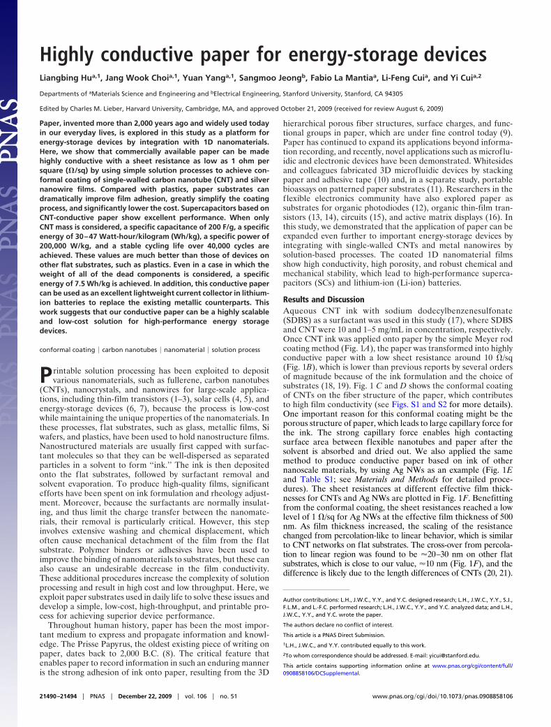
Results and DiscussionAqueous CNT ink with sodium dodecylbenzenesulfonate(SDBS) as a surfactant was used in this study (17), where SDBSand CNT were 10 and 1–5 mg/mL in concentration, respectively.Once CNT ink was applied onto paper by the simple Meyer rodcoating method (Fig. 1A), the paper was transformed into highlyconductive paper with a low sheet resistance around 10 �/sq(Fig. 1B), which is lower than previous reports by several ordersof magnitude because of the ink formulation and the choice ofsubstrates (18, 19). Fig. 1 C and D shows the conformal coatingof CNTs on the fiber structure of the paper, which contributesto high film conductivity (see Figs. S1 and S2 for more details).One important reason for this conformal coating might be theporous structure of paper, which leads to large capillary force forthe ink. The strong capillary force enables high contactingsurface area between flexible nanotubes and paper after thesolvent is absorbed and dried out. We also applied the samemethod to produce conductive paper based on ink of othernanoscale materials, by using Ag NWs as an example (Fig. 1Eand Table S1; see Materials and Methods for detailed proce-dures). The sheet resistances at different effective film thick-nesses for CNTs and Ag NWs are plotted in Fig. 1F. Benefittingfrom the conformal coating, the sheet resistances reached a lowlevel of 1 �/sq for Ag NWs at the effective film thickness of 500nm. As film thickness increased, the scaling of the resistancechanged from percolation-like to linear behavior, which is similarto CNT networks on flat substrates. The cross-over from percola-tion to linear region was found to be �20–30 nm on other flatsubstrates, which is close to our value, �10 nm (Fig. 1F), and thedifference is likely due to the length differences of CNTs (20, 21).
Author contributions: L.H., J.W.C., Y.Y., and Y.C. designed research; L.H., J.W.C., Y.Y., S.J.,F.L.M., and L.-F.C. performed research; L.H., J.W.C., Y.Y., and Y.C. analyzed data; and L.H.,J.W.C., Y.Y., and Y.C. wrote the paper.
The authors declare no conflict of interest.
This article is a PNAS Direct Submission.
1L.H., J.W.C., and Y.Y. contributed equally to this work.
2To whom correspondence should be addressed. E-mail: [email protected].
This article contains supporting information online at www.pnas.org/cgi/content/full/0908858106/DCSupplemental.
21490–21494 � PNAS � December 22, 2009 � vol. 106 � no. 51 www.pnas.org�cgi�doi�10.1073�pnas.0908858106
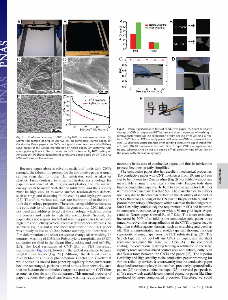
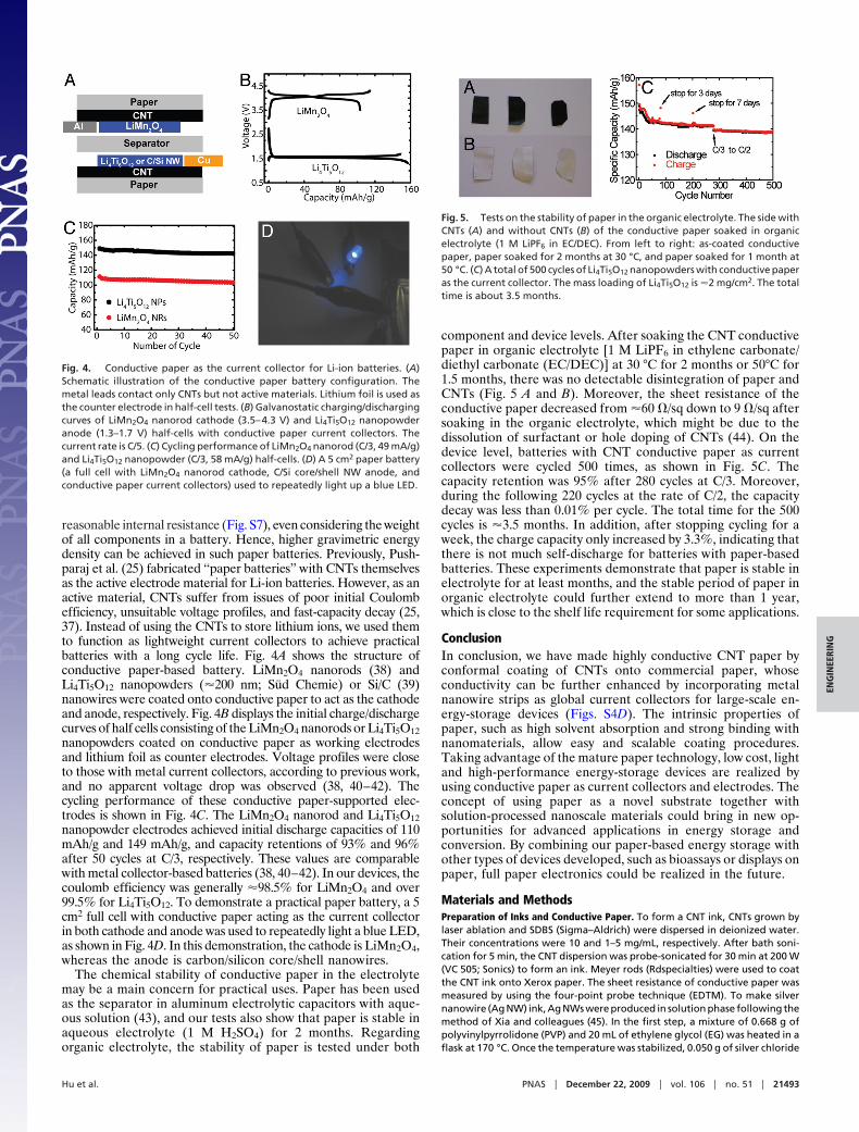
Because paper absorbs solvents easily and binds with CNTsstrongly, the fabrication process for the conductive paper is muchsimpler than that for other flat substrates, such as glass orplastics. First, contrary to other substrates, ink rheology forpaper is not strict at all. In glass and plastics, the ink surfaceenergy needs to match with that of substrates, and the viscositymust be high enough to avoid surface tension-driven defects,such as rings and dewetting in the coating and drying processes(22). Therefore, various additives are incorporated in the ink totune the rheology properties. These insulating additives decreasethe conductivity of the final film. In contrast, our CNT ink doesnot need any additives to adjust the rheology, which simplifiesthe process and leads to high film conductivity. Second, thepaper does not require surfactant washing processes to achievehigh film conductivity, which is necessary for other substrates. Asshown in Fig. 2 A and B, the sheet resistance of the CNT paperwas already as low as 30 �/sq before washing, and there was nofilm delamination and sheet resistance change after washing. Incontrast, washing of CNTs on Polyethylene terephthalate (PET)substrates resulted in significant film cracking and peel-off (Fig.2B). The local resistance of CNT film on PET decreasedsignificantly (Fig. S3A); however, the global resistance became�1,000 times higher (Fig. 2 A). Although the detailed mecha-nism behind this unusual phenomenon is unclear, it is likely thatwhile solvent is sucked into paper by capillary force, surfactantsbecome rearranged, perhaps toward porous fiber networks, suchthat surfactants do not hinder charge transport within CNT filmsas much as they do with flat substrates. This unusual property ofpaper renders the typical surfactant washing requirement un-
necessary in the case of conductive paper, and thus its fabricationprocess becomes greatly simplified.
The conductive paper also has excellent mechanical properties.The conductive paper with CNT thicknesses from 100 nm to 5 �mcan be bent down to a 2-mm radius (Fig. 2C) or folded without anymeasurable change in electrical conductivity. Fatigue tests showthat the conductive paper can be bent to a 2-mm radius for 100 timeswith resistance increase less than 5%. These mechanical behaviorsare likely due to the combined effect of the flexibility of individualCNTs, the strong binding of the CNTs with the paper fibers, and theporous morphology of the paper, which can relax the bending strain.Such flexibility could satisfy the requirement in SCs and batteries.In comparison, conductive paper with a 50-nm gold layer evapo-rated on Xerox paper showed Rs of 7 �/sq. The sheet resistanceincreased by 50% after folding the conductive gold paper threetimes. Moreover, the strong adhesion of the CNTs to paper lead tohigh film stability against damage, such as scratching and peeling-off. This is demonstrated via a Scotch tape test showing the clearsuperiority of using paper over the PET substrate (Fig. 2D). TheScotch tape did not peel off any CNTs on paper, and the sheetresistance remained the same, �10 �/sq. As in the conformalcoating, the exceptionally strong binding is attributed to the largecapillary force and maximized contact area and, subsequently, Vander Waals force between the CNTs and paper (23). The superiorflexibility and high stability make conductive paper promising forvarious rolled-up devices. It is noteworthy that the conductive paperdescribed here is completely distinct from previously reported bulkypapers (24) or other conductive paper (25) in several perspectives.(i) We used widely available commercial paper, not paper-like filmsproduced by more complicated processes. Therefore, we could
Fig. 1. Conformal coating of CNTs or Ag NWs on commercial paper. (A)Meyer rod coating of CNT or Ag NW ink on commercial Xerox paper. (B)Conductive Xerox paper after CNT coating with sheet resistance of �10 �/sq.SEM images of (C) surface morphology of Xerox paper, (D) conformal CNTcoating along fibers in Xerox paper, and (E) conformal Ag NW coating onXerox paper. (F) Sheet resistances of conductive paper based on CNTs and AgNWs with various thicknesses.
Fig. 2. Various performance tests of conductive paper. (A) Sheet resistancechange of CNTs on paper and PET before and after the process of washing toremove surfactants. (B) The comparison of film peeling after washing surfac-tants. CNT films on PET are easily peeled off, whereas CNTs on paper still stickwell. (C) Sheet resistance changes after bending conductive paper into differ-ent radii. (D) Film adhesion test with Scotch tape: CNTs on paper remainbound, whereas CNTs on PET are peeled off. (E) Direct writing of CNT ink onthe paper with Chinese calligraphy.
Hu et al. PNAS � December 22, 2009 � vol. 106 � no. 51 � 21491
ENG
INEE
RIN
G

benefit from the well-established paper technology. (ii) Our con-ductive paper takes advances of intrinsic properties of paper, whichlargely simplifies the fabrication process. (iii) Our fabrication pro-cess is scalable, with roll-to-roll fashion. (iv) Other painting methodscan also be applied to fabricate conductive paper. Chinese callig-raphy (Fig. 2E) and pen writing (Fig. S3B) are demonstrated asexamples.
Because of the high conductivity and the large surface area, theconductive paper was studied in SC applications as active electrodesand current collectors. CNTs deposited on porous paper are moreaccessible to ions in the electrolyte than those on flat substrates (6,26–33), which can result in high power density. In addition, thepaper itself can function well as a separator. Therefore, all-paperSCs have been realized by simple fabrication processes (Fig. 3A).We fabricated such all-paper SCs and tested their performance in
both aqueous and organic electrolytes by using galvanostatic (Fig.3B) and cyclic voltammetric (Fig. S5) methods. Detailed proceduresfor the device preparation and performance characterization aredescribed in Materials and Methods and SI Materials and Methods.As shown in Fig. 3C, the specific capacitances of all-paper SCs atvarious currents are superior to the previously reported values withpure CNT electrodes on flat substrates (6, 26–33), and are evenclose to those of pseudocapacitors based on the polymer/CNTcomposites (34, 35). A high specific capacitance of 200 F/g wasachieved for devices in sulfuric acid electrolyte (Fig. 3C). Further-more, our devices can maintain excellent specific capacitance evenunder high-current operations. Even at �40 A/g, capacitanceslarger than 70 F/g were maintained in both aqueous and organicphases. Such high capacitances at large currents are attributed tothe excellent ion accessibility from both sides of the CNT film andintimate electrolyte–CNT wetting that originates from the porousnature of paper. For comparison, PET-based SCs prepared in thesame way only showed capacity less than 50 F/g, (Fig. 3C), whichindicates the importance of the porous nature of paper for betterSC performance. This is also confirmed by another control exper-iment with Au conductive paper. Devices with the same amount ofCNTs on Au-coated Xerox paper (50 nm, 7 �/sq) showed 36 F/g at10 A/g, which is 4 � 5-fold lower than our CNT conductive paperSCs (�160 F/g at the same current density). This is likely becausethe Au film blocks pores in paper and impedes the ion access fromthe paper side. When operated at 3 V in organic solvent, the specificenergy and power reached 47 Wh/kg and 200,000 W/kg, respec-tively, which exceed previously reported data (Fig. 3D) (6, 26, 27,30, 31). Our data in this plot are calculated based on CNT mass onlyto compare with other data in the references that were also acquiredin the same way. Furthermore, even in a case when CNT massloading increased to 1.7 mg/cm2, the device performance was stillsuperior to others reported (Fig. 3D). The superior capacitancesmay be a result of the higher ion accessibility in the paper due tothe strong absorption of solvent by the paper. The CNT film onpaper is also thinner, with the same mass loading as a result of thelarger surface area of the rough paper. Also, to compare withcommercial devices (36) and see the significance of mass saving byreplacing metal current collectors with conductive paper, we plot-ted another Ragone plot (Fig. 3E). In this plot, the mass of deadcomponents (electrolyte, paper, separator � 1.1, 3.3, 1.6 mg/cm2,respectively) was considered in addition to active materials(CNTs � 1.7 mg/cm2). This Ragone plot shows that our data arebetter in both energy/power densities compared with commercialdevices as well as reported data in the literature (33) that are alsobased on the mass of all of the device components.
Cycle life, one of the most critical parameters in the SC opera-tions, turns out to be excellent for 40,000 cycles (Fig. 3F). Only 3%and 0.6% capacitance losses were observed in sulfuric acid andorganic electrolyte, respectively. Moreover, the conductive paperwas mechanically robust and did not show any cracks or evidenceof breakage for 60 days. CNT films as thick as �14 �m (1.33mg/cm2) were also tested in sulfuric acid, and capacitances as highas �122 F/g were achieved (Fig. S6B). The devices with 1.33 and 1.7mg/cm2 CNTs were compared with the reported densest CNTassembly data (Fig. S6C) (28). Our devices show larger capacitancesper area compared with their films, although their films are 10 timesthicker. Furthermore, their devices also leave plenty of unusedspace, and therefore might not be scalable. More data on cyclicvoltammetry (CV; Fig. S5) and thickness dependence of thecapacitance (Fig. S6A) are presented in the SI Materials andMethods.
Rechargeable batteries are another type of energy-storagedevice with high energy density, but they are still too heavy forapplications such as vehicle electrification. In this work, con-ductive paper was used to replace the heavy metallic currentcollectors, which could reduce the weight of batteries up to 20%(Table S2; see SI Materials and Methods for details) with
Fig. 3. Conductive paper as SC electrodes. (A) Schematic illustration ofall-paper SCs based on CNT conductive paper. Zoomed-in schematic illustratesthat ion accessibility is enhanced by the strong solvent absorption. (B) Gal-vanostatic charging/discharging curves taken from 3 V with organic electro-lyte and 1 V with sulfuric acid. (C) Gravimetric capacitances at various currentsmeasured in aqueous and organic electrolytes. Data from CNTs on PET areplotted together for comparison. (D) A Ragone plot showing that the all-paper SCs outperform the PET SC devices and reported data in literature (6, 26,27, 30, 31). The color coding (black, red, green) of the traces is the same as inC. Data in B–D as well as data from references mentioned in D are calculatedbased on a mass loading of CNTs only. Typical mass CNT loadings in C and D are72 �g/cm2, and data from a large mass loading of 1.7 mg/cm2 are alsopresented (D, blue plot). (E) A Ragone plot based on the mass of differentcombinations of dead components. A plot from ref. 33 based on the mass ofentire device components is also presented. The trapezoid showing the per-formance of commercial devices is from ref. 36. (F) Capacitance retentionmeasured in different electrolytes. After 40,000 cycles, 97% and 99.4% ofinitial capacitances are maintained for sulfuric acid and organic electrolytes,respectively.
21492 � www.pnas.org�cgi�doi�10.1073�pnas.0908858106 Hu et al.
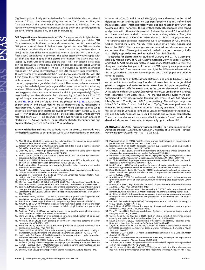
reasonable internal resistance (Fig. S7), even considering the weightof all components in a battery. Hence, higher gravimetric energydensity can be achieved in such paper batteries. Previously, Push-paraj et al. (25) fabricated ‘‘paper batteries’’ with CNTs themselvesas the active electrode material for Li-ion batteries. However, as anactive material, CNTs suffer from issues of poor initial Coulombefficiency, unsuitable voltage profiles, and fast-capacity decay (25,37). Instead of using the CNTs to store lithium ions, we used themto function as lightweight current collectors to achieve practicalbatteries with a long cycle life. Fig. 4A shows the structure ofconductive paper-based battery. LiMn2O4 nanorods (38) andLi4Ti5O12 nanopowders (�200 nm; Sud Chemie) or Si/C (39)nanowires were coated onto conductive paper to act as the cathodeand anode, respectively. Fig. 4B displays the initial charge/dischargecurves of half cells consisting of the LiMn2O4 nanorods or Li4Ti5O12nanopowders coated on conductive paper as working electrodesand lithium foil as counter electrodes. Voltage profiles were closeto those with metal current collectors, according to previous work,and no apparent voltage drop was observed (38, 40–42). Thecycling performance of these conductive paper-supported elec-trodes is shown in Fig. 4C. The LiMn2O4 nanorod and Li4Ti5O12nanopowder electrodes achieved initial discharge capacities of 110mAh/g and 149 mAh/g, and capacity retentions of 93% and 96%after 50 cycles at C/3, respectively. These values are comparablewith metal collector-based batteries (38, 40–42). In our devices, thecoulomb efficiency was generally �98.5% for LiMn2O4 and over99.5% for Li4Ti5O12. To demonstrate a practical paper battery, a 5cm2 full cell with conductive paper acting as the current collectorin both cathode and anode was used to repeatedly light a blue LED,as shown in Fig. 4D. In this demonstration, the cathode is LiMn2O4,whereas the anode is carbon/silicon core/shell nanowires.
The chemical stability of conductive paper in the electrolytemay be a main concern for practical uses. Paper has been usedas the separator in aluminum electrolytic capacitors with aque-ous solution (43), and our tests also show that paper is stable inaqueous electrolyte (1 M H2SO4) for 2 months. Regardingorganic electrolyte, the stability of paper is tested under both
component and device levels. After soaking the CNT conductivepaper in organic electrolyte [1 M LiPF6 in ethylene carbonate/diethyl carbonate (EC/DEC)] at 30 °C for 2 months or 50°C for1.5 months, there was no detectable disintegration of paper andCNTs (Fig. 5 A and B). Moreover, the sheet resistance of theconductive paper decreased from �60 �/sq down to 9 �/sq aftersoaking in the organic electrolyte, which might be due to thedissolution of surfactant or hole doping of CNTs (44). On thedevice level, batteries with CNT conductive paper as currentcollectors were cycled 500 times, as shown in Fig. 5C. Thecapacity retention was 95% after 280 cycles at C/3. Moreover,during the following 220 cycles at the rate of C/2, the capacitydecay was less than 0.01% per cycle. The total time for the 500cycles is �3.5 months. In addition, after stopping cycling for aweek, the charge capacity only increased by 3.3%, indicating thatthere is not much self-discharge for batteries with paper-basedbatteries. These experiments demonstrate that paper is stable inelectrolyte for at least months, and the stable period of paper inorganic electrolyte could further extend to more than 1 year,which is close to the shelf life requirement for some applications.
ConclusionIn conclusion, we have made highly conductive CNT paper byconformal coating of CNTs onto commercial paper, whoseconductivity can be further enhanced by incorporating metalnanowire strips as global current collectors for large-scale en-ergy-storage devices (Figs. S4D). The intrinsic properties ofpaper, such as high solvent absorption and strong binding withnanomaterials, allow easy and scalable coating procedures.Taking advantage of the mature paper technology, low cost, lightand high-performance energy-storage devices are realized byusing conductive paper as current collectors and electrodes. Theconcept of using paper as a novel substrate together withsolution-processed nanoscale materials could bring in new op-portunities for advanced applications in energy storage andconversion. By combining our paper-based energy storage withother types of devices developed, such as bioassays or displays onpaper, full paper electronics could be realized in the future.
Materials and MethodsPreparation of Inks and Conductive Paper. To form a CNT ink, CNTs grown bylaser ablation and SDBS (Sigma–Aldrich) were dispersed in deionized water.Their concentrations were 10 and 1–5 mg/mL, respectively. After bath soni-cation for 5 min, the CNT dispersion was probe-sonicated for 30 min at 200 W(VC 505; Sonics) to form an ink. Meyer rods (Rdspecialties) were used to coatthe CNT ink onto Xerox paper. The sheet resistance of conductive paper wasmeasured by using the four-point probe technique (EDTM). To make silvernanowire (Ag NW) ink, Ag NWs were produced in solution phase following themethod of Xia and colleagues (45). In the first step, a mixture of 0.668 g ofpolyvinylpyrrolidone (PVP) and 20 mL of ethylene glycol (EG) was heated in aflask at 170 °C. Once the temperature was stabilized, 0.050 g of silver chloride
Fig. 4. Conductive paper as the current collector for Li-ion batteries. (A)Schematic illustration of the conductive paper battery configuration. Themetal leads contact only CNTs but not active materials. Lithium foil is used asthe counter electrode in half-cell tests. (B) Galvanostatic charging/dischargingcurves of LiMn2O4 nanorod cathode (3.5–4.3 V) and Li4Ti5O12 nanopowderanode (1.3–1.7 V) half-cells with conductive paper current collectors. Thecurrent rate is C/5. (C) Cycling performance of LiMn2O4 nanorod (C/3, 49 mA/g)and Li4Ti5O12 nanopowder (C/3, 58 mA/g) half-cells. (D) A 5 cm2 paper battery(a full cell with LiMn2O4 nanorod cathode, C/Si core/shell NW anode, andconductive paper current collectors) used to repeatedly light up a blue LED.
Fig. 5. Tests on the stability of paper in the organic electrolyte. The side withCNTs (A) and without CNTs (B) of the conductive paper soaked in organicelectrolyte (1 M LiPF6 in EC/DEC). From left to right: as-coated conductivepaper, paper soaked for 2 months at 30 °C, and paper soaked for 1 month at50 °C. (C) A total of 500 cycles of Li4Ti5O12 nanopowders with conductive paperas the current collector. The mass loading of Li4Ti5O12 is �2 mg/cm2. The totaltime is about 3.5 months.
Hu et al. PNAS � December 22, 2009 � vol. 106 � no. 51 � 21493
ENG
INEE
RIN
G
(AgCl) was ground finely and added to the flask for initial nucleation. After 3minutes, 0.22 g of silver nitrate (AgNO3) was titrated for 10 minutes. Then, theflask was kept at the same temperature for another 30 minutes. After thereaction was completed, the solution was cooled down and centrifuged threetimes to remove solvent, PVP, and other impurities.
Cell Preparation and Measurements of SCs. For aqueous electrolyte devices,two pieces of CNT conductive paper were first attached on glass slides. CNTfilms were used as both electrodes and current collectors. At the end of theCNT paper, a small piece of platinum was clipped onto the CNT conductivepaper by a toothless alligator clip to connect to a battery analyzer (Maccor4300). Both glass slides were assembled with a separator (Whatman 8-�mfilter paper) sandwiched in between. The paper assembly was wrapped withparafilm and then dipped in the electrolyte solution. The active area over-lapped by both CNT conductive papers was 1 cm2. For organic electrolytedevices, cells were assembled by inserting the same separator soaked with thestandard battery electrolyte (1 M LiPF6 in ethylene carbonate:diethylenecarbonate � 1:1 vol/vol; Ferro) between two CNT conductive paper substrates.The active area overlapped by both CNT conductive paper substrates was also1 cm2. Then, the entire assembly was sealed in a polybag (Sigma–Aldrich). Asin the aqueous cells, small pieces of platinum were attached to the end of CNTconductive paper for a good electrical contact. The current collectors came outthrough the sealed edges of polybags and then were connected to the batteryanalyzer. All steps in the cell preparation were done in an argon-filled glovebox (oxygen and water contents below 1 and 0.1 ppm, respectively). Typicalmass loadings for data shown in the main text Fig. 3 C and D are 72 � 270�g/cm2. Larger mass loadings up to 1.7 mg/cm2 were also tested (Fig. 3 D andE, and Fig. S6C), and the capacitances are plotted in Fig. S6. Capacitance,energy density, and power density are all characterized by galvanostaticmeasurements. A total of 0.02 � 20 mA/cm2 were applied to cells whilepotentials between both electrodes swept between cutoff values (0 � V �
0.85 � 1 V in aqueous phase, 0 � V �2.3 � 3 V in organic phase). Voltages wererecorded every 0.01 � 0.2 seconds. For the cycling test in both phases ofelectrolyte, �5 A/g was applied. The cutoff potentials for the sulfuric acid andorganic electrolyte were 0.85 and 2.3 V, respectively.
Battery Fabrication and Test. The cathode materials LiMn2O4 nanorods weresynthesized according to our previous work, with modification (38). Typically,
8 mmol MnSO4�H2O and 8 mmol (NH4)2S2O8 were dissolved in 20 mL ofdeionized water, and the solution was transferred to a 45-mL, Teflon-linedstainless steel vessel (Parr). The vessel was sealed and heated at 150 °C for 12 hto obtain �-MnO2 nanorods. The as-synthesized MnO2 nanorods were mixedand ground with lithium acetate (Aldrich) at a molar ratio of 2:1. A total of 1mL of methanol was added to make a uniform slurry mixture. Then, themixture was sintered at 700 °C for 10 h under air to obtain LiMn2O4 nanorods.The carbon/silicon core/shell nanowires were synthesized by CVD method.Carbon nanofibers (Sigma–Aldrich) were loaded into a tube furnace andheated to 500 °C. Then, silane gas was introduced and decomposed ontocarbon nanofibers. The weight ratio of silicon shell to carbon core was typically�2:1. Li4Ti5O12 powder was used as received from Sud Chemie.
Electrodes for electrochemical studies of LiMn2O4 and Li4Ti5O12 were pre-pared by making slurry of 70 wt % active materials, 20 wt % Super P Carbon,and 10 wt % PVDF binder in N-methyl-2-pyrrolidone (NMP) as the solvent. Theslurry was coated onto a piece of conductive CNT paper by an applicator andthen dried at 100 °C in a vacuum oven overnight. For C/Si core/shell nanowires,the as-synthesized nanowires were dropped onto a CNT paper and dried toform the anode.
The half-cell tests of both cathode (LiMn2O4) and anode (Li4Ti5O12) werecarried out inside a coffee bag (pouch) cell assembled in an argon-filledglovebox (oxygen and water contents below 1 and 0.1 ppm, respectively).Lithium metal foil (Alfa Aesar) was used as the counter electrode in each case.A 1 M solution of LiPF6 in EC/DEC (1:1 vol/vol; Ferro) was used as the electrolyte,with separators from Asahi Kasei. The charge/discharge cycles were per-formed at different rates at room temperature, where 1C was 148 mA/g forLiMn2O4 and 175 mA/g for Li4Ti5O12, respectively. The voltage range was3.5–4.3 V for LiMn2O4 and 1.3–1.7 V for Li4Ti5O12. Tests were performed byeither Bio-Logic VMP3 battery testers or MTI battery analyzers. To fabricate afull cell with high voltage to light a blue LED, silicon/carbon core/shell nanow-ires and LiMn2O4 nanorods were used as anode and cathode, respectively.Then, the two electrodes were assembled to make a 5 cm2 pouch cell asdescribed above, and it was used to repeatedly light the blue LED.
ACKNOWLEDGMENTS. This work was supported by The Korea Foundation forAdvanced Studies (S.J.) and King Abdullah University of Science and Technol-ogy Investigator Award KUS-l1-001-12 (to Y.C.).
1. Ahn JH, et al. (2006) Heterogeneous three-dimensional electronics by use of printedsemiconductor nanomaterials. Science 314:1754–1757.
2. Talapin DV, Murray CB (2005) PbSe nanocrystal solids for n- and p-channel thin filmfield-effect transistors. Science 310:86–89.
3. Duan XF, et al. (2003) High-performance thin-film transistors using semiconductornanowires and nanoribbons. Nature 425:274–278.
4. Kim JY, et al. (2007) Efficient tandem polymer solar cells fabricated by all-solutionprocessing. Science 317:222–225.
5. Bach U, et al. (1998) Solid-state dye-sensitized mesoporous TiO2 solar cells with highphoton-to-electron conversion efficiencies. Nature 395:583–585.
6. An KH, et al. (2001) Supercapacitors using single-walled carbon nanotube electrodes.Adv Mater 13:497–500.
7. Poizot P, et al. (2000) Nano-sized transition-metaloxides as negative-electrode mate-rials for lithium-ion batteries. Nature 407:496–499.
8. Edwards IES, Hammond NGL, Gadd CJ (1975) The Cambridge Ancient History (Cam-bridge Univ Press, Cambridge, UK).
9. Roberts JC (1996) Paper Chemistry (Springer, New York).10. Martinez AW, Phillips ST, Whitesides GM (2008) Three-dimensional microfluidic de-
vices fabricated in layered paper and tape. Proc Natl Acad Sci USA 105:19606–19611.11. Carrilho E, Martinez AW, Whitesides GM (2009) Understanding wax printing: A simple
micropatterning process for paper-based microfluidics. Anal Chem 81:7091–7095.12. Lamprecht B, et al. (2005) Organic photodiodes on newspaper. Physica Status Solidi A
202:R50–R52.13. Kaihovirta NWC, Makela T, Wilen C, Osterbacka R (2009) Self-supported ion-
conductive membrane-based transistors. Adv Mater 21:2520–2523.14. Eder F, et al. (2004) Organic electronics on paper. Appl Phys Lett 84:2673–2675.15. Kim DHK, et al. (2009) Ultrathin silicon circuits with strain-isolation layers and mesh
layouts for high-performance electronics on fabric, vinyl, leather, and paper. AdvMater 21:3703–3707.
16. Anderson P, et al. (2002) Active matrix displays based on all-organic electrochemicalsmart printed on paper. Adv Mater 14:1460–1464.
17. Islam MF, et al. (2003) High weight fraction surfactant solubilization of single-wallcarbon nanotubes in water. Nano Lett 3:269–273.
18. Kordas K, et al. (2006) Inkjet printing of electrically conductive patterns of carbonnanotubes. Small 2:1021–1025.
19. Hecht DS, Hu L, Gruner G (2007) Electronic properties of carbon nanotube/fabriccomposites. Curr Appl Phys 7:60–63.
20. Doherty EDS, et al. (2009) The spatial uniformity and electromechanical stability oftransparent, conductive films of single walled nanotubes. Carbon 47:2466–2473.
21. Hu L, Hecht DS, Gruner G (2004) Percolation in transparent and conducting carbonnanotube networks. Nano Lett 4:2513–2517.
22. Gutoff EB, Cohen ED (2006) Coating and Drying Defects: Troubleshooting OperatingProblems (Society of Plastics Engineers Monographs), (John Wiley & Sons, Hoboken, NJ).
23. Hertel T, Walkup REAP (1998) Deformation of carbon nanotubes by surface van derWaals forces. Phys Rev B 58:13870–13873.
24. Endo M, et al. (2005) ‘Buckypaper’ from coaxial nanotubes. Nature 433:476–476.
25. Pushparaj VL, et al. (2007) Flexible energy storage devices based on nanocompositepaper. Proc Natl Acad Sci USA 104:13574–13577.
26. Kaempgen M, et al. (2009) Printable thin film supercapacitors using single-walledcarbon nanotubes. Nano Lett 9:1872–1876.
27. Kimizuka O, et al. (2008) Electrochemical doping of pure single-walled carbon nano-tubes used as supercapacitor electrodes. Carbon 46:1999–2001.
28. Futaba DN, et al. (2006) Shape-engineerable and highly densely packed single-walled carbonnanotubes and their application as super-capacitor electrodes. Nat Mater 5:987–994.
29. Du CS, Pan N (2006) Supercapacitors using carbon nanotubes films by electrophoreticdeposition. J Power Sources 160:1487–1494.
30. Ma RZ, et al. (1999) Processing and performance of electric double-layer capacitorswith block-type carbon nanotube electrodes. Bull Chem Soc Jpn 72:2563–2566.
31. Zhou CF, Kumar S, Doyle CD, Tour JM (2005) Functionalized single wall carbon nano-tubes treated with pyrrole for electrochemical supercapacitor membranes. ChemMater 17:1997–2002.
32. Ahn HJ, et al. (2006) Electrochemical capacitors fabricated with carbon nanotubesgrown within the pores of anodized aluminum oxide templates. Electrochem Comm8:513–516.
33. Niu CM, et al. (1997) High power electrochemical capacitors based on carbon nanotubeelectrodes. Appl Phys Lett 70:1480–1482.
34. Malinauskas A, Malinauskiene J, Ramanavicius A (2005) Conducting polymer-basednanostructurized materials: Electrochemical aspects. Nanotechnology 16:R51–R62.
35. An KH, et al. (2002) High-capacitance supercapacitor using a nanocomposite electrodeof single-walled carbon nanotube and polypyrrole. J Electrochem Soc 149:A1058–A1062.
36. Pandolfo AG, Hollenkamp AF (2006) Carbon properties and their role in supercapaci-tors. J Power Sources 157:11–27.
37. Landi BJ, et al. (2008) Lithium ion capacity of single wall carbon nanotube paperelectrodes. J Phys Chem C 112:7509–7515.
38. Yang Y, et al. (2009) Single nanorod devices for battery diagnostics: A case study ofLiMn2O4. Nano Lett, in press.
39. Cui LF, Yang Y, Hsu CM, Cui Y (2009) Carbon-silicon core-shell nanowires as highcapacity electrode for lithium ion batteries. Nano Lett 9:3370–3376.
40. Kavan L, Gratzel M (2002) Facile synthesis of nanocrystalline Li4Ti5O12 (spinel) exhib-iting fast Li insertion. Electrochem Solid State Lett 5:A39–A42.
41. Zaghib K, Simoneau M, Armand M, Gauthier M (1999) Electrochemical study ofLi4Ti5O12 as negative electrode for Li-ion polymer rechargeable batteries. J PowerSources 81:300–305.
42. Thackeray MM, et al. (1984) Electrochemical extraction of lithium from Limn2o4. MaterRes Bull 19:179–187.
43. Muriset G (1952) Influence of the impurities in the foil, electrolyte and paper in theelectrolytic capacitor. J Power Source 99:285–288.
44. Zhou WVJ, et al. (2005) Charge transfer and Fermi level shift in p-doped single-walledcarbon nanotubes. Phys Rev B 71:205423.
45. Sun YG, Mayers B, Herricks T, Xia YN (2003) Polyol synthesis of uniform silver nanow-ires: A plausible growth mechanism and the supporting evidence. Nano Lett 3:955–960.
21494 � www.pnas.org�cgi�doi�10.1073�pnas.0908858106 Hu et al.