Embed Size (px)
Citation preview

© July 11, 2017 Dr. Lynn Fuller and Dr. Ivan Puchades
High Voltage Process Integration
Page 1
ROCHESTER INSTITUTE OF TECHNOLOGYMICROELECTRONIC ENGINEERING
High Voltage and MEMS Process Integration
Dr. Lynn Fuller and Dr. Ivan Puchadeswebpage: http://people.rit.edu/lffeee
Electrical and Microelectronic EngineeringRochester Institute of Technology
82 Lomb Memorial DriveRochester, NY 14623-5604
email: [email protected] program webpage: http://www.rit.edu/kgcoe/microelectronic/
7-11-2017 HV_Integration.pptx
© July 11, 2017 Dr. Lynn Fuller and Dr. Ivan Puchades
High Voltage Process Integration
Page 2
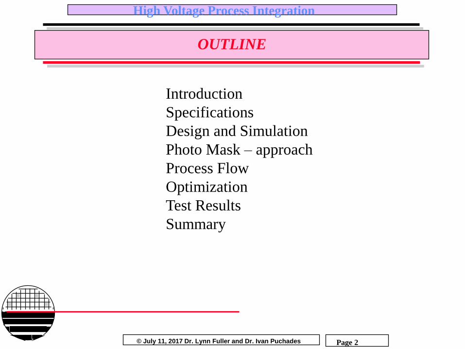
OUTLINE
Introduction
Specifications
Design and Simulation
Photo Mask – approach
Process Flow
Optimization
Test Results
Summary

© July 11, 2017 Dr. Lynn Fuller and Dr. Ivan Puchades
High Voltage Process Integration
Page 3
DESIGN AND FABRICATE LARGE INK JET PRINT HEAD
2-inch wide ink jet print head chip design such that 1inch 700 jet cell can be copied and pasted to make larger print heads up to 6 inch width. Each ink jet (cell) is 240um high and 600um wide. The 1 inch wide array is 15 rows and 42 columns. Shown above is 2 inch wide array of 2800 individual ink jets.
© July 11, 2017 Dr. Lynn Fuller and Dr. Ivan Puchades
High Voltage Process Integration
Page 4
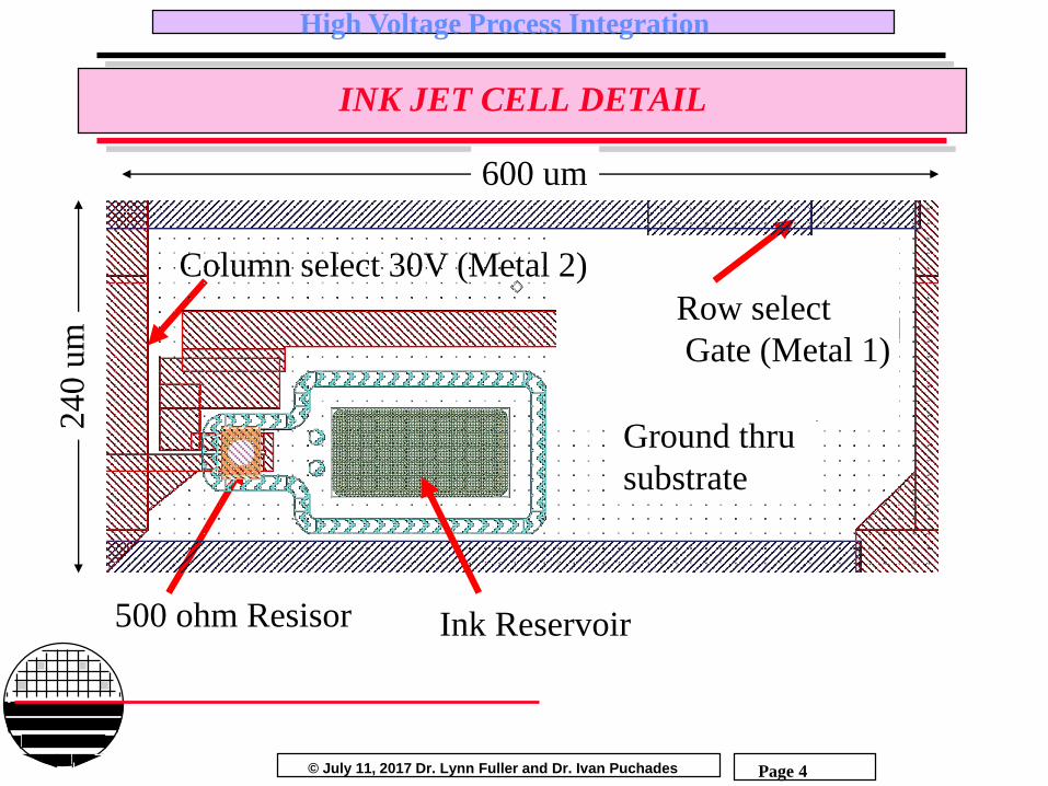
INK JET CELL DETAIL
500 ohm Resisor Ink Reservoir
Row select
Gate (Metal 1)
Column select 30V (Metal 2)
Ground thru
substrate
600 um
240 u
m

© July 11, 2017 Dr. Lynn Fuller and Dr. Ivan Puchades
High Voltage Process Integration
Page 5
ADDRESSING SINGLE INK JET CELL
Row
Column
Resistor
NMOS
CONSIDERATIONS
Gate Delay (propagation along two inch metal line connected to 47 gate capacitances)
Resistance to ground (should be as low as possible)
NMOSFETVoltages and Currents
RESISTORThermal properties

© July 11, 2017 Dr. Lynn Fuller and Dr. Ivan Puchades
High Voltage Process Integration
Page 6
SPICE SIMULATION OF 1us PULSE PROPAGATION
3) 1um thick, 4” Al line, 1usec signal:1) 1um thick, 2” Al line, 1usec signal:
4) 0.75um thick, 4” Al line, 1usec signal:2) 0.75um thick, 2” Al line, 1usec signal:
Simulation: Uniform Distributed RC Lines (Lossy) is used. Model needs resistance and capacitance per unit length as input.

© July 11, 2017 Dr. Lynn Fuller and Dr. Ivan Puchades
High Voltage Process Integration
Page 7
CALCULATION OF RESISTANCE TO GROUND
Equivalent model for wafer, to be used in calculation:
P++ substrate
P- epiR epi
R substrate
R = R epi + R substrate
Where:
T = Thickness of the region
p = Resistivity of the material
W, L= Width, length of the top rectangle
a = Ratio of the width of the bottom rectangle to the width of top rectangle
b = Ratio of the length of the bottom rectangle to the length of the top rectangle
cm015.0
cm 6
675um
10um
W1, L1
W2, L2
W3, L3
T
T
(Gray and Meyer)
ba
b
aln
WL
TR

© July 11, 2017 Dr. Lynn Fuller and Dr. Ivan Puchades
High Voltage Process Integration
Page 8
CALCULATION OF RESISTANCE TO GROUND
W1 = 70um L1 = 230umW2 = 90um L2 = 250umW3 = 1440um L3 = 1600um
So, the dimensions are:
230
250
70
90
)230/250
70/90ln(
um230xum70
um10xcm6epiR
250
1600
90
1440
)250/1600
90/1440ln(
um250xum90
um675xcm015.0substrateR
R = R epi + R substrate = 31.91 ohms, and the potential drop across this R = 1.28V
In the circuit, the source resistor should not have a voltage across it
more than 2V, this means: R source x 40mA < 2V, R source < 50ohms
and the answer is 31.48
and the answer is 0.43

© July 11, 2017 Dr. Lynn Fuller and Dr. Ivan Puchades
High Voltage Process Integration
Page 9
NMOSFET V, I AND SIZE REQUIREMENTS
High Voltage on Drain and Gate
•Vgate either 5, 10, 15 or 20V (determined by address electronics)
•Vdrain=30V
•Idrain= ~ 40mA (determines size of transistor)
•Transistor Size Requirements - Matrix set up:
•Cells are 240um high and 600um wide
•Approximately 240x350um for transistor
Location of
NMOSFET

© July 11, 2017 Dr. Lynn Fuller and Dr. Ivan Puchades
High Voltage Process Integration
Page 10
NMOSFET VOLTAGES
ON – VGATE=15V and VDD=30V – ID=40mA, VDS=10V
OFF – VGATE=0V and VDD=30V
VGATE=15V and VDD = 0V
Column VDD =30V
Row
VGATE =15V
ID=40mAR=500 Ohm
VDS=10V
R=500 Ohm
VDS=30V
C o lu m n V D D = 3 0 V
R o w
V G A T E = 0 V
ID=0A
Resistance
to ground?

© July 11, 2017 Dr. Lynn Fuller and Dr. Ivan Puchades
High Voltage Process Integration
Page 11
HIGH VOLTAGE TRANSISTORS
• Thick gate oxides to prevent gate oxide breakdown (30 Volts)• Low doping on both sides of drain-to-well pn junction to give large depletion width, low electric field and give high breakdown voltage.•Deep drain junctions to increase radius of curvature, reduce electric field and give high breakdown voltage.•Long channel length to prevent punch through
P++
P- epi
N+N-XoxMetal Gate

© July 11, 2017 Dr. Lynn Fuller and Dr. Ivan Puchades
High Voltage Process Integration
Page 12
NMOSFET PROCESS SIMULATION
Lower Doped Drain Well - HVNW
P+ Contact to
Substrate and
Ground
N+ DrainN+ Source
Metal Gate
Channel Stop
Channel length is ~3µm. Good alignment between N+ source and HVNW is required.
P-well
Silvaco Athena

© July 11, 2017 Dr. Lynn Fuller and Dr. Ivan Puchades
High Voltage Process Integration
Page 13
NMOS TRANSISTOR CONSIDERATIONS
qNaBV
Si
2
2
max
N/P Junction Reverse Bias Breakdown.
V
I
Forward BiasReverse Bias
Breakdown
N+ P 0V30V
Max E field in Si is 3E5V/cm
Breakdown voltage is related to the concentration of lower doped side

© July 11, 2017 Dr. Lynn Fuller and Dr. Ivan Puchades
High Voltage Process Integration
Page 14
NMOS TRANSISTOR CONSIDERATIONS
BV dependence of junction depth and curvature
*

© July 11, 2017 Dr. Lynn Fuller and Dr. Ivan Puchades
High Voltage Process Integration
Page 15
NMOS TRANSISTOR CALCULATIONS
•With Vdrain=30V-Make Gate oxide 1000Å, Ey=3.0MV/cm-C’ox=3.45E-8F/cm2
•Threshold voltage with NA=3.5E15/cm3 is –0.865VT adjust implant needed for VT=1 is Boron, dose=8E11/cm2
+/- Vt = q Dose”/Cox’
•N+/PW build in voltage = 0.85VWith VR=30V, Wd=3.35um, =1.84E5V/cm <3E5V/cm
ssFBTNVV ox
ox
msFB
C
QV
'
' tFs
42
i
A
F
n
N
q
kTln
ox
Asi
C
Nq
'
2
WdW1W2= [ (2siqF +VR) (1/NA 1/ND)]1/2
= - [(2q/si F+VR) (NA ND/(NA ND))]1/2 Volts/cm

© July 11, 2017 Dr. Lynn Fuller and Dr. Ivan Puchades
High Voltage Process Integration
Page 16
NMOSFET SIMULATIONS
Emax=1.6e5V/cm<E
crit(3e5V/cm)
Emax=1.2e5V/cm<E
crit(3e5V/cm)Equipotential lines in the
HVNW with VD>35V.
Silvaco
P-EPI
NA

© July 11, 2017 Dr. Lynn Fuller and Dr. Ivan Puchades
High Voltage Process Integration
Page 17
NMOSFET ELECTRICAL SIMULATIONS
For VG=10VIDS/W=100µA/µmW for 60mA=600µm
For VG=20VIDS/W=350µA/µmW for 60mA=171µm
For VG=5VIDS/W=60µA/µmW for 60mA=1000µm
Channel W set to 210µm
Silvaco – Atlas

© July 11, 2017 Dr. Lynn Fuller and Dr. Ivan Puchades
High Voltage Process Integration
Page 18
MASK MAKING
RIT Price is $500 each = ~$8,000
Commercial Price is $2000 each = ~$32,000
RIT Mask Making Capabilities (MEBES Electron Beam Writer)
1X masks for RIT Karl Suss Aligner (6”x 6”x 0.090”) – Qty 3
5X masks for RIT ASML I-Line Stepper (6”x 6 x 0.120”) – Qty 3
1X masks for Company’s Karl Suss Aligner (6”x 6”x 0.090”) – Qty 5
5X masks for Company’s Canon Stepper (6” x 6” x 0.250”) – Qty 5

© July 11, 2017 Dr. Lynn Fuller and Dr. Ivan Puchades
High Voltage Process Integration
Page 19
FOURTEEN DIFFERENT MASKS USED
•RIT layers::•layer 99 -> Alignment keys 5X•layer 1 -> Active 1X •layer 4 -> Nplus 5X•layer 6 -> HVNW 5X •layer 3 -> Pplus 1X•layer 7 -> Contact cut 1X•layer 24 -> 60 Metal1 1X (Lab’s 1st)
•Company’s Research Lab layers::•layer 15 -> 30 Metal2•layer 29 -> 70 Via•layer 30 -> 80 Heater•layer 34 -> 90 Feed Channel •layer 37 -> 96 Backside holes•layer 19 -> Polyimide chamber•layer 25 -> 04 Nozzles

© July 11, 2017 Dr. Lynn Fuller and Dr. Ivan Puchades
High Voltage Process Integration
Page 20
PROCESS FLOW
1. Initial 100 Silicon, boron=3.5E152. Alignment layer photo –
5X Stepper- dark field reticle3. Alignment etch – Silicon etch4. Grow 500Å oxide (43min at 1000C)5. Deposit 1500Å Si3N4
P-EPI
SiO2Si3N4
Photoresist
P+ P+
6. Active photo – 1X – clear field7. Nitride etch (LAM490)8. Channel stop boron implant
Dose=5e12, 80KeV9. Strip resist, RCA Clean
© July 11, 2017 Dr. Lynn Fuller and Dr. Ivan Puchades
High Voltage Process Integration
Page 21
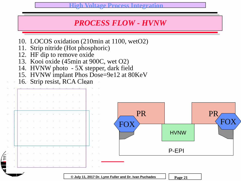
PROCESS FLOW - HVNW
PR PR
P-EPI
FOX FOX
HVNW
10. LOCOS oxidation (210min at 1100, wetO2)11. Strip nitride (Hot phosphoric)12. HF dip to remove oxide13. Kooi oxide (45min at 900C, wet O2)14. HVNW photo - 5X stepper, dark field15. HVNW implant Phos Dose=9e12 at 80KeV16. Strip resist, RCA Clean

© July 11, 2017 Dr. Lynn Fuller and Dr. Ivan Puchades
High Voltage Process Integration
Page 22
22
N++ S/D
17. HVNW Drive, 90min at 1100C, N218. VT adjust implant boron
1.1e12, 60KeV1.1e12, 100KeV
19. N+ Photo – 5X stepper, dark field20. N+ Implant Phos 4e15, 100KeV21. Strip resist, RCA Clean
P-EPI
FOX FOX
HVNW
PR
N+ N+N+

© July 11, 2017 Dr. Lynn Fuller and Dr. Ivan Puchades
High Voltage Process Integration
Page 23
P++ SUBSTRATE CONTACT
22. P+ Photo – 1X dark field
23. P+ Implant Boron 2e15, 60KeV
24. Strip resist, RCA Clean
25. Remove Kooi oxide – 1 min HF
P++ P++
P-EPI
HVNW
N+ N+N+
© July 11, 2017 Dr. Lynn Fuller and Dr. Ivan Puchades
High Voltage Process Integration
Page 24
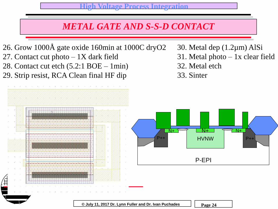
METAL GATE AND S-S-D CONTACT
26. Grow 1000Å gate oxide 160min at 1000C dryO2
27. Contact cut photo – 1X dark field
28. Contact cut etch (5.2:1 BOE – 1min)
29. Strip resist, RCA Clean final HF dip
30. Metal dep (1.2µm) AlSi
31. Metal photo – 1x clear field
32. Metal etch
33. Sinter
P++ P++
P-EPI
HVNW
N+ N+N+
© July 11, 2017 Dr. Lynn Fuller and Dr. Ivan Puchades
High Voltage Process Integration
Page 25
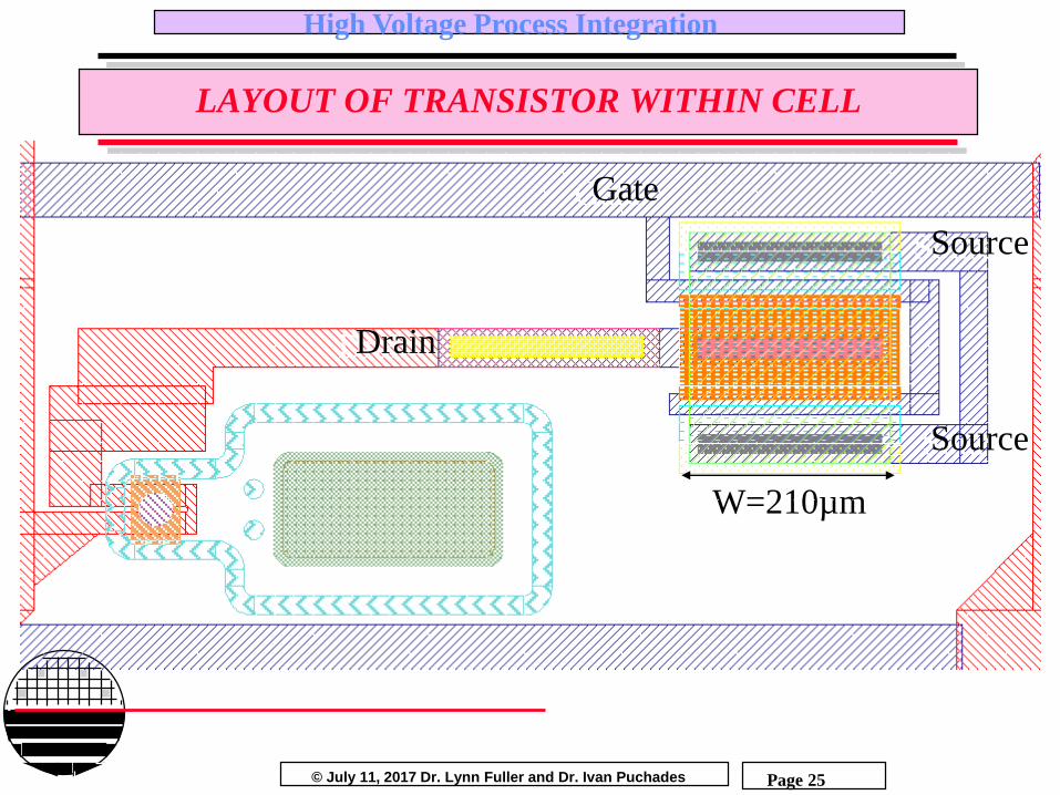
LAYOUT OF TRANSISTOR WITHIN CELL
W=210µm
Source
Source
Gate
Drain
Source
Source
Gate
Drain

© July 11, 2017 Dr. Lynn Fuller and Dr. Ivan Puchades
High Voltage Process Integration
Page 26
LAYOUT AND PHOTO
N+
N+
N+
P+
P+
P-channel and HVNW
P-channel and HVNW
I
I

© July 11, 2017 Dr. Lynn Fuller and Dr. Ivan Puchades
High Voltage Process Integration
Page 27
1st LOT L070619
•1st lot – L070619
•Channel Stop – 8e13, 100KeV•HVNW – 9e12, 120KeV•HVNW drive – 210min + O2
•IDS(VG=20V)=85mA•ILK(VD=20V)=20mA•BVDSS=20V•HVNW to N+ seemed shorted.
•Reduce HVNW drive.

© July 11, 2017 Dr. Lynn Fuller and Dr. Ivan Puchades
High Voltage Process Integration
Page 28
2nd LOT L070712
•2nd lot – L070712
•Channel stop – 8e13, 100KeV•HVNW – 9e12, 80KeV•HVNW drive – 140min++O2
•IDS=55mA•ILK(VD=20V)=10µA •BVDSS=20V
•Remove O2 from HVNW drive.•Increase BVDSS.•1X alignment issues. •6-inch mask holder.

© July 11, 2017 Dr. Lynn Fuller and Dr. Ivan Puchades
High Voltage Process Integration
Page 29
4th LOT L070907
•4th lot – L070907•Channel stop – 8e13, 80/100KeV•HVNW – 9e12/1e13, 80KeV•HVNW drive – 90/120min nit
•IDS=53mA•ILK=1µA•BVDSS=22V
•HVNW drive needs to be shorten even further.•Low leakage for wafer with 90min and 9e12 dose after sinter.•Channel stop implant dose reduction
120min Drive
90min Drive
© July 11, 2017 Dr. Lynn Fuller and Dr. Ivan Puchades
High Voltage Process Integration
Page 30
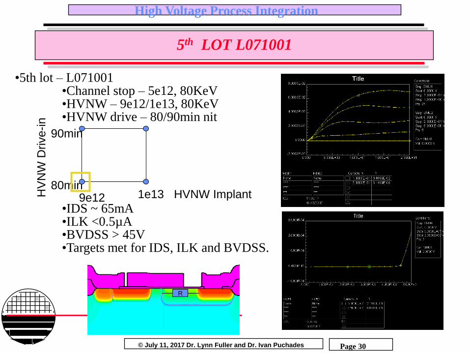
5th LOT L071001
•5th lot – L071001•Channel stop – 5e12, 80KeV•HVNW – 9e12/1e13, 80KeV•HVNW drive – 80/90min nit
•IDS ~ 65mA•ILK <0.5µA•BVDSS > 45V•Targets met for IDS, ILK and BVDSS.
9e12 1e1380min
90min
HVNW Implant HV
NW
Drive-in
R
© July 11, 2017 Dr. Lynn Fuller and Dr. Ivan Puchades
High Voltage Process Integration
Page 31
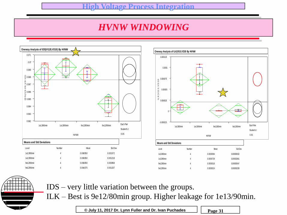
HVNW WINDOWING
IDS – very little variation between the groups.
ILK – Best is 9e12/80min group. Higher leakage for 1e13/90min.
ID
S(V
G2
0,V
D1
0)
0.062
0.063
0.064
0.065
0.066
0.067
0.068
0.069
0.07
0.071
1e13/80min 1e13/90min 9e12/80min 9e12/90min
HVNW
Each Pair
Student's t
0.05
1e13/80min
1e13/90min
9e12/80min
9e12/90min
Level
4
4
4
4
Number
0.068350
0.069350
0.068350
0.064375
Mean
0.001572
0.001218
0.000858
0.001207
Std Dev
Means and Std Deviations
Oneway Analysis of IDS(VG20,VD10) By HVNW
IL
K(V
G0
,V
D3
0
-0.000025
0
0.000025
0.00005
0.000075
0.0001
0.000125
1e13/80min 1e13/90min 9e12/80min 9e12/90min
HVNW
Each Pair
Student's t
0.05
1e13/80min
1e13/90min
9e12/80min
9e12/90min
Level
4
4
4
4
Number
0.0000094
0.0000729
0.0000018
0.0000024
Mean
0.00000632
0.00002841
0.00000047
0.00000209
Std Dev
Means and Std Deviations
Oneway Analysis of ILK(VG0,VD30 By HVNW

© July 11, 2017 Dr. Lynn Fuller and Dr. Ivan Puchades
High Voltage Process Integration
Page 32
BEST NMOSFET RESULTS

© July 11, 2017 Dr. Lynn Fuller and Dr. Ivan Puchades
High Voltage Process Integration
Page 33
CONCLUSION
•Successful development and fabrication of a 30V high-side NMOS transistor.
•IDS, ILK and BVDSS requirements have been met.
•Robust process flow has been designed and demonstrated.
•Fabrication of ~20 wafers has been completed.
•Continuous process improvement to reduce ILK even further and improve drain series resistance.
© July 11, 2017 Dr. Lynn Fuller and Dr. Ivan Puchades
High Voltage Process Integration
Page 34
TEXTBOOK/REFERENCES
1. Modern Semiconductor Devices for Integrated Circuits, Chenming Hu, Prentice Hall, 2010.
2. Solid State Electronic Devices, 5th Edition, Ben Streetman, Sanjay Banerjee, Prentice Hall, 2000.
3. Silicon VLSI Technology, James Plummer, Michael Deal, Peter Griffin, Prentice Hall, 2000.
4. Analysis and Design of Analog Integrated Circuits, Gray and Meyer, John Wiley.