Embed Size (px)
Citation preview
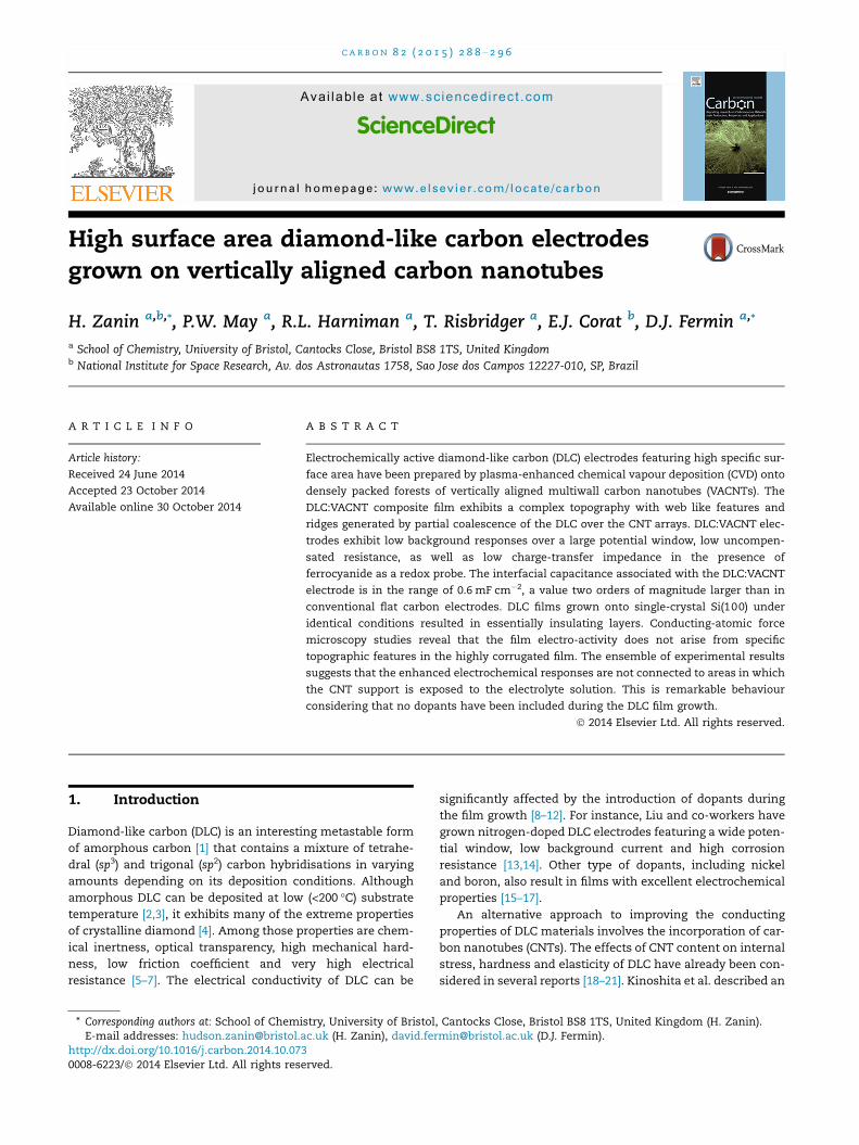
C A R B O N 8 2 ( 2 0 1 5 ) 2 8 8 – 2 9 6
.sc iencedi rect .com
Avai lab le at wwwScienceDirect
journal homepage: www.elsev ier .com/ locate /carbon
High surface area diamond-like carbon electrodesgrown on vertically aligned carbon nanotubes
http://dx.doi.org/10.1016/j.carbon.2014.10.0730008-6223/� 2014 Elsevier Ltd. All rights reserved.
* Corresponding authors at: School of Chemistry, University of Bristol, Cantocks Close, Bristol BS8 1TS, United Kingdom (H. ZE-mail addresses: [email protected] (H. Zanin), [email protected] (D.J. Fermin).
H. Zanin a,b,*, P.W. May a, R.L. Harniman a, T. Risbridger a, E.J. Corat b, D.J. Fermin a,*
a School of Chemistry, University of Bristol, Cantocks Close, Bristol BS8 1TS, United Kingdomb National Institute for Space Research, Av. dos Astronautas 1758, Sao Jose dos Campos 12227-010, SP, Brazil
A R T I C L E I N F O
Article history:
Received 24 June 2014
Accepted 23 October 2014
Available online 30 October 2014
A B S T R A C T
Electrochemically active diamond-like carbon (DLC) electrodes featuring high specific sur-
face area have been prepared by plasma-enhanced chemical vapour deposition (CVD) onto
densely packed forests of vertically aligned multiwall carbon nanotubes (VACNTs). The
DLC:VACNT composite film exhibits a complex topography with web like features and
ridges generated by partial coalescence of the DLC over the CNT arrays. DLC:VACNT elec-
trodes exhibit low background responses over a large potential window, low uncompen-
sated resistance, as well as low charge-transfer impedance in the presence of
ferrocyanide as a redox probe. The interfacial capacitance associated with the DLC:VACNT
electrode is in the range of 0.6 mF cm�2, a value two orders of magnitude larger than in
conventional flat carbon electrodes. DLC films grown onto single-crystal Si(100) under
identical conditions resulted in essentially insulating layers. Conducting-atomic force
microscopy studies reveal that the film electro-activity does not arise from specific
topographic features in the highly corrugated film. The ensemble of experimental results
suggests that the enhanced electrochemical responses are not connected to areas in which
the CNT support is exposed to the electrolyte solution. This is remarkable behaviour
considering that no dopants have been included during the DLC film growth.
� 2014 Elsevier Ltd. All rights reserved.
1. Introduction
Diamond-like carbon (DLC) is an interesting metastable form
of amorphous carbon [1] that contains a mixture of tetrahe-
dral (sp3) and trigonal (sp2) carbon hybridisations in varying
amounts depending on its deposition conditions. Although
amorphous DLC can be deposited at low (<200 �C) substrate
temperature [2,3], it exhibits many of the extreme properties
of crystalline diamond [4]. Among those properties are chem-
ical inertness, optical transparency, high mechanical hard-
ness, low friction coefficient and very high electrical
resistance [5–7]. The electrical conductivity of DLC can be
significantly affected by the introduction of dopants during
the film growth [8–12]. For instance, Liu and co-workers have
grown nitrogen-doped DLC electrodes featuring a wide poten-
tial window, low background current and high corrosion
resistance [13,14]. Other type of dopants, including nickel
and boron, also result in films with excellent electrochemical
properties [15–17].
An alternative approach to improving the conducting
properties of DLC materials involves the incorporation of car-
bon nanotubes (CNTs). The effects of CNT content on internal
stress, hardness and elasticity of DLC have already been con-
sidered in several reports [18–21]. Kinoshita et al. described an
anin).
C A R B O N 8 2 ( 2 0 1 5 ) 2 8 8 – 2 9 6 289
interesting approach to creating high surface area DLC struc-
tures via microwave plasma chemical vapour deposition
(MPCVD) growth onto vertically aligned carbon nanotube
(VACNT) arrays featuring number densities 1–7 · 109 cm�2
[22]. Recently, Zanin and co-workers developed a similar
approach to prepare high surface area DLC electrodes show-
ing excellent field emission properties [23]. Different DLC-
coated CNT microstructures such as ‘teepees’, elongated
ridges or ‘honeycombs’ were fabricated by tuning parameters
such as the VACNT number density and DLC deposition
conditions.
In the present work, we show for the first time that highly
corrugated DLC films grown on VACNTs exhibit high electro-
activity without the introduction of additional dopants. The
as-grown DLC on VACNT (DLC:VACNT) were characterised
by reversible electrochemical responses in the presence of
ferrocyanide, with double layer capacitance larger than
0.6 mF cm�2. DLC films grown on Si (100) wafers (DLC:Si)
under identical conditions yielded inherently insulating lay-
ers. Conducting atomic force microscopy (AFM) measure-
ments confirmed that the electroactivity of DLC:VACNT is
not linked to specific topographic features in the highly corru-
gated films, with large portions of the surface exhibiting sim-
ilar conductance values.
2. Experimental
2.1. Preparation of VACNT films
VACNT films were produced using a microwave plasma (MP)
CVD chamber operating at 2.45 GHz [24]. Substrates were Ti
sheets (10 mm · 10 mm · 0.5 mm) covered with a 10 nm Ni
layer deposited by electron-beam evaporation. The Ni layer
was heated from 350 to 800 �C over a period of 5 min in a
N2/H2 (10/90 sccm) plasma, inducing the formation of nano-
particles which promote the CNT growth. VACNT growth
was initiated by introducing CH4 (14 sccm) into the chamber
for 1 min, maintaining a substrate temperature of 800 �Cand a reactor pressure of 30 torr. After growth, the sample
was placed in a plasma enhanced chemical vapour deposition
(PECVD) reactor (�400 V, pulse frequency 20 kHz) with an oxy-
gen flow rate of 1 sccm at a pressure of 5 mtorr for 1 min. This
was done in order to improve wettability and create oxygen-
functional groups on the VACNT surfaces [25].
2.2. DLC film growth
DLC layers were deposited using a PECVD reactor fed with
hexane vapour and argon gas at 0.1–0.3 torr and a discharge
voltage of �700 V at a pulse frequency of 20 kHz. For prepara-
tion of the composite DLC:VACNT samples, the previously
prepared VACNT forest samples were used as substrates.
Before growth, n-hexane was sprayed onto the samples and
then the plasma was struck under argon and n-hexane vapour
for 10 min [23].
Flat DLC electrodes were deposited onto a polished silicon
(100) substrate for use as control samples. To prepare these,
a Si wafer was placed into the PECVD reactor and cleaned using
an argon plasma atmosphere at 0.1 torr (Ar flow rate of 1 sccm)
for 30 min. Next, n-hexane was sprayed into the active plasma
region via a nozzle which directed downwards onto the sub-
strate surface for 1 h for 1 lm DLC deposition, with Ar flowing
during the whole process. After deposition, the DLC:Si samples
were cooled down in high vacuum (10�6 torr) for 3 h [26].
2.3. Instrumentation and chemicals
DLC samples were characterised by high-resolution scanning
electron microscopy (HR-SEM), Raman spectroscopy, tunnel-
ling AFM and electrochemical tests. HR-SEM was performed
with a FEI Inspect F50 operated at 20–30 kV. Raman spectra
were recorded at room temperature using a Renishaw micro-
probe, employing argon-ion laser excitation (k = 514.5 nm)
with a laser power of �6 mW and a spot size �15 lm. Curve
fitting and data analysis Fityk software was used to assigned
the peak locations and fit all spectra. The tunnelling AFM
measurements were performed with a Bruker Multimode
with Nanoscope V controller with Picoforce Extender.
Cyclic voltammetry (CV) and electrochemical impedance
spectroscopy (EIS) were recorded with an Autolab PGSTAT30
potentiostat. The electrochemical responses of DLC grown
on either Si or VACNTwere measured in Ar-saturated aqueous
electrolyte solutions containing KNO3 and K4Fe(CN)6 as the
supporting electrolyte and redox probe, respectively. The geo-
metrical surface area of the working electrode was defined by
using chemically-inert adhesive 3M Teflon tape to mask off
some of the film, leaving a 3-mm-diameter open hole of fixed
area (0.071 cm2). The electrical contact was made on the top
of the electrode using silver paste and copper wire. Ag/AgCl
(in saturated KCl) and a pure platinum mesh were employed
as reference and counter electrodes, respectively. All chemi-
cals and electrodes were purchased from Sigma Aldrich.
3. Results and discussion
3.1. Structural characterisation of the DLC layers
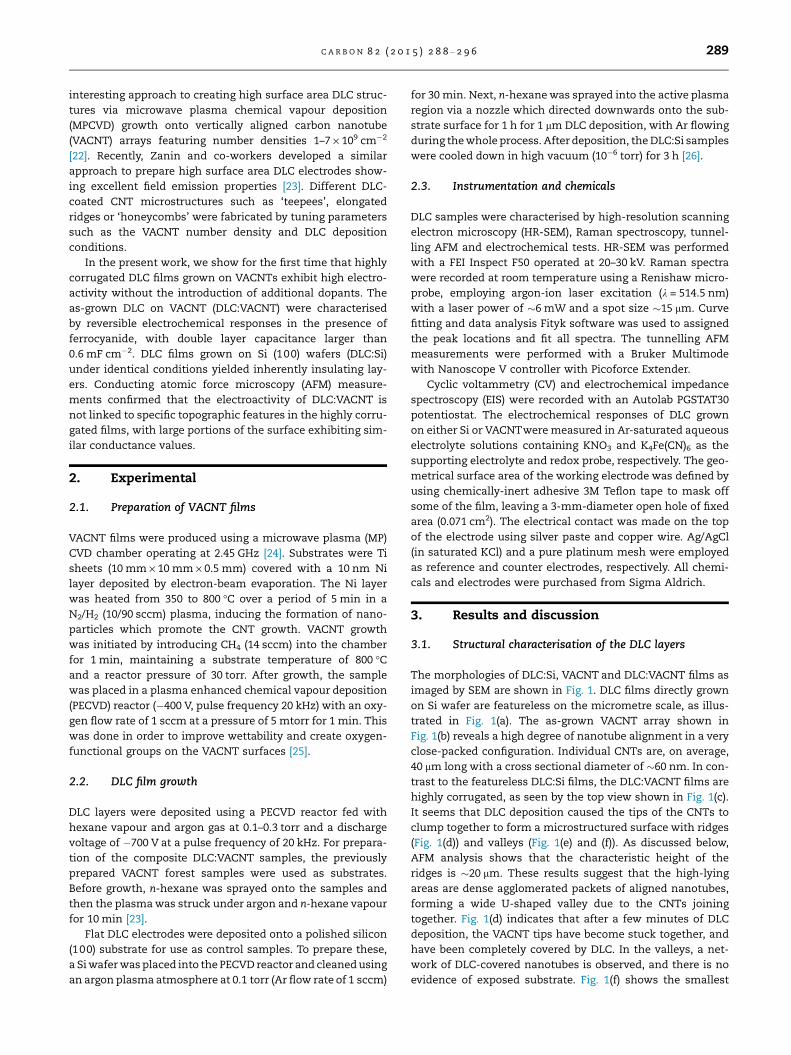
The morphologies of DLC:Si, VACNT and DLC:VACNT films as
imaged by SEM are shown in Fig. 1. DLC films directly grown
on Si wafer are featureless on the micrometre scale, as illus-
trated in Fig. 1(a). The as-grown VACNT array shown in
Fig. 1(b) reveals a high degree of nanotube alignment in a very
close-packed configuration. Individual CNTs are, on average,
40 lm long with a cross sectional diameter of �60 nm. In con-
trast to the featureless DLC:Si films, the DLC:VACNT films are
highly corrugated, as seen by the top view shown in Fig. 1(c).
It seems that DLC deposition caused the tips of the CNTs to
clump together to form a microstructured surface with ridges
(Fig. 1(d)) and valleys (Fig. 1(e) and (f)). As discussed below,
AFM analysis shows that the characteristic height of the
ridges is �20 lm. These results suggest that the high-lying
areas are dense agglomerated packets of aligned nanotubes,
forming a wide U-shaped valley due to the CNTs joining
together. Fig. 1(d) indicates that after a few minutes of DLC
deposition, the VACNT tips have become stuck together, and
have been completely covered by DLC. In the valleys, a net-
work of DLC-covered nanotubes is observed, and there is no
evidence of exposed substrate. Fig. 1(f) shows the smallest
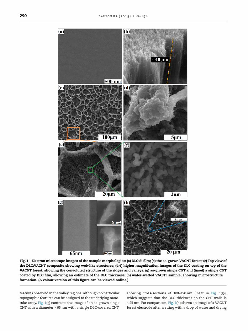
Fig. 1 – Electron microscope images of the sample morphologies: (a) DLC:Si film; (b) the as-grown VACNT forest; (c) Top view of
the DLC:VACNT composite showing web-like structures; (d–f) higher magnification images of the DLC coating on top of the
VACNT forest, showing the convoluted structure of the ridges and valleys; (g) as-grown single CNT and (inset) a single CNT
coated by DLC film, allowing an estimate of the DLC thickness; (h) water-wetted VACNT sample, showing microstructure
formation. (A colour version of this figure can be viewed online.)
290 C A R B O N 8 2 ( 2 0 1 5 ) 2 8 8 – 2 9 6
features observed in the valley regions, although no particular
topographic features can be assigned to the underlying nano-
tube array. Fig. 1(g) contrasts the image of an as-grown single
CNT with a diameter �65 nm with a single DLC-covered CNT,
showing cross-sections of 100–120 nm (inset in Fig. 1(g)),
which suggests that the DLC thickness on the CNT walls is
�25 nm. For comparison, Fig. 1(h) shows an image of a VACNT
forest electrode after wetting with a drop of water and drying
C A R B O N 8 2 ( 2 0 1 5 ) 2 8 8 – 2 9 6 291
at room temperature. The water causes the CNT tips to stick
together, forming a microstructure similar to that showed in
Fig. 1(c). These structures are formed as surface tension
forces on the wet CNT pulled them together. Even after water
has evaporated away, the CNTs remain weakly bonded by van
der Waals forces. The similarity of these to the structures in
Fig. 1(c) suggests that DLC deposition acts in a similar way,
sticking the CNTs together by the surface tension of hexane
vapour used for the DLC growth.
Fig. 2 contrasts the Raman spectra of DLC films grown on
VACNTs and on the Si wafer, as well as the as-grown VACNT
array. The spectrum of the DLC:Si film (Fig. 2(b)) exhibits two
broad bands centred at 1340 cm�1 (D-band) and 1537 cm�1
(G-band), arising from breathing and stretching vibrational
modes of sp2 carbon sites, respectively [23,27,28]. The spec-
trum from the as-grown VACNT arrays (Fig. 2(c)) can be decon-
voluted into five distinct bands, including the sharp D and
G-bands at 1357 and 1585 cm�1, respectively. The D-band for
CNTs is related to defects and disordered carbon whilst the
G-band (E2g) is related to well-ordered crystalline graphite
[29]. Other modes include the so-called D 0-band (1622 cm�1)
commonly associated with disordered carbon structures [25],
the band at 1230 cm�1 attributed to various vibrational modes
close to the K point, and the 1480 cm�1 band linked to nano-
Fig. 2 – (a) Raman spectra of DLC:Si, DLC:VACNT and VACNT sam
DLC:VACNT are deconvoluted as described in the main text. (A
sized carbon or trans-polyacetylene [31]. The Raman spectrum
of the DLC:VACNT sample (Fig. 2(d)) appears as a combination
of the DLC and VACNT Raman characteristics [26]. These
observations suggest that the integrity of the individual CNTs
is not affected by the subsequent DLC growth [23].
The presence of hydrogen in the PECVD process ensures
that H will be incorporated in these DLC films, meaning,
strictly speaking, they should be described as hydrogenated
amorphous carbon films (a–C:H). The hydrogen atoms are
mainly bonded to olefinic groups leading to a high content
of sp3 carbon in the DLC film, probably in the form of pendant
CH2 or CH3 groups [30]. Based on the analysis reported by Fer-
rari et al. [31] the Raman intensity ratio ID/IG can be used to
estimate the sp3 carbon content and the optical band gap
[32,33]. In the case of the DLC:Si film, the observed ratio
ID/IG = 0.28 is consistent with an sp3 carbon content of 60–70%
and an optical band gap of 2.0–2.5 eV. For the DLC:VACNT film
ID/IG = 0.52, which corresponds to 45–55% sp3 carbon and a
smaller band gap of between 1.6 and 1.8 eV.
3.2. Electrochemical properties of DLC:VACNT films
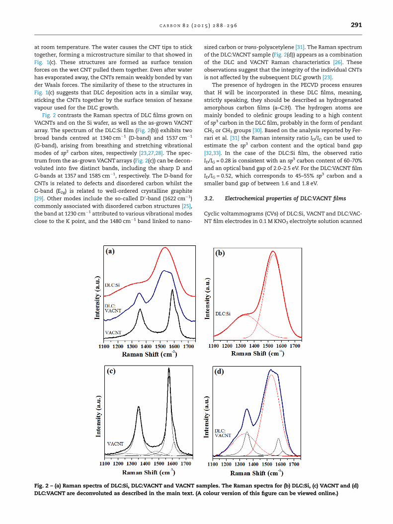
Cyclic voltammograms (CVs) of DLC:Si, VACNT and DLC:VAC-
NT film electrodes in 0.1 M KNO3 electrolyte solution scanned
ples. The Raman spectra for (b) DLC:Si, (c) VACNT and (d)
colour version of this figure can be viewed online.)
Fig. 3 – (a) Cyclic voltammograms from DLC:Si, VACNT and DLC:VACNT electrodes (electrode surface area 0.07 cm2) taken at
100 mV s�1 in 0.1 M KNO3. The CV from DLC:Si is shown as a dotted red horizontal line due to its insulating nature. Cyclic
voltammetry from (b) VACNT and (c) DLC-coated VACNT electrodes in 0.1 M KNO3 taken at different scan rates from 50, 75 and
100 mV s�1. (A colour version of this figure can be viewed online.)
Fig. 4 – (a) Comparison of CV curves of 1 mM potassium ferrocyanide in 0.1 M potassium nitrate for DLC:Si, VACNT and
DLC:VACNT electrodes (electrode surface area 0.07 cm2) taken at a constant 100 mV s�1 scan rate. (b) CV responses obtained
using DLC-coated VACNT electrodes in 1 mM potassium ferrocyanide in 0.1 M potassium nitrate taken at different scan rates
(10, 25, 50, 75, 100 mV s�1). (A colour version of this figure can be viewed online.)
Fig. 5 – Impedance spectra taken at the formal redox potential of the ferro/ferricyanide couple for DLC:Si, VACNT and
DLC:VACNT electrodes. The electrolyte contains 1 mM potassium ferrocyanide with 0.1 M potassium nitrate aqueous
solution. The data are presented as Bode plots: (a) the modulus of the impedance amplitude |Z|, and (b) the phase of the
impedance response versus the frequency. (A colour version of this figure can be viewed online.)
292 C A R B O N 8 2 ( 2 0 1 5 ) 2 8 8 – 2 9 6
at 100 mV s�1 are displayed in Fig. 3(a). There is a remarkable
contrast between the background current observed for
the DLC films on Si with respect to those on VACNT. The
DLC:VACNT electrode exhibits capacitive currents comparable
to those obtained for the VACNT films, with a similar
potential window. A broadening of the capacitive current for
C A R B O N 8 2 ( 2 0 1 5 ) 2 8 8 – 2 9 6 293
VACNT films at potentials above 0.3 V is consistent with the
formation of oxygenated groups at the surface of the nano-
tubes. This response is significantly suppressed in the case
of DLC:VACNT. In the case of DLC:Si, the film effectively
behaves as a highly insulating layer. This behaviour is consis-
tent with conventional DLC films grown in the absence of
doping elements [4,26,34].
Fig. 3(b and c) displays the CVs of (b) VACNT and (c)
DLC:VACNT electrodes as a function of the potential scan
rate. The potential range was narrowed down in order to
avoid interferences from the Faradaic responses associated
with the oxygenated surface functional groups. The capaci-
tive current increases linearly with the potential scan rate,
resulting in a differential capacitance of 875 and 642 lF cm�2
for (b) VACNT and (c) DLC:VACNT at 0.15 V. Considering that
typical double-layer capacitance values for carbon electrodes
are of the order of 5 lF cm�2 [35], it can be estimated
that the roughness factor associated with the DLC:VACNT
electrode is approximately 130. If we consider a similar
specific capacitance for VACNT and DLC:VACNT, this result
suggests that the DLC growth leads to a 32 ± 4% decrease
in the electroactive surface area. This observation appears
consistent with the CNT bundling induced by the DLC
growth. However, it should also be considered that other
parameters can also play a role in changes of the double-
layer capacitance in these highly porous assemblies, such
as surface wettability and the penetration of the electrolyte
solution.
Characteristic voltammograms for the various carbon
electrodes in the presence of 1 · 10�3 mol dm�3 K4Fe(CN)6 at
100 mV s�1 are shown in Fig. 4(a). While VACNT and DLC:VAC-
NT electrodes show well-defined redox responses, no clear
faradaic signals are observed for DLC:Si films. An interesting
observation is the slight offset in the potential of the redox
responses for the VACNT electrode with respect to the
DLC:VACNT electrode. This is associated with generation of
Donnan potentials with the highly porous carbon nanotube
arrays. These phenomena will be investigated in more detail
in a separate communication. In the case of DLC:VACNT, a
high degree of reversibility is observed at various scan rates,
as shown in Fig. 4(b). The peak currents are proportional to
the square root of the scan rate, which allow estimating a dif-
fusion coefficient of the redox probe of 7 · 10�6 cm2 s�1 based
on Randles–Sevcik equation [36].
Further evidence of the electroactive nature of the DLC
film grown on VACNT arrays is illustrated by the electrochem-
ical impedance spectra shown in Fig. 5. The magnitude of the
impedance amplitude (|Z|) is several orders higher for the
DLC:Si film than for the DLC:VACNT film. The growth of DLC
leads to an increase of |Z| with respect to that from VACNT.
The frequency dependence of the amplitude and phase is
compatible with a conventional Randles model in the case
of DLC:VACNT and VACNT over significant portions of the fre-
quency range. In contrast, DLC:Si is characterised by quasi-
capacitive behaviour over the entire frequency range. The
DLC:VACNT spectra has been fitted to the Randles model
down to frequencies of 1 Hz. The impedance analysis resulted
in values for uncompensated resistance of 216 ± 6 X, a War-
burg element (Yo) of 0.22 m s0.5 O-1 (consistent with the diffu-
sion coefficient of the redox probe) and capacitance from
double layer formation of (45 ± 3) · 10�6 F.
At frequencies below 1 Hz, the diffusion kinetics within
the porous nature of the electrodes can be probed. This
behaviour is determined by the phase angle above the 45�limit expected for planar diffusion. This trend is more
pronounced in the case of the VACNT electrode indicating
that the thin DLC layer decreases the porosity of the DLC to
a certain extent. In order to fully describe the impedance
responses over the entire potential range, more complex
equivalent circuits should be used, incorporating transmis-
sion lines. For the purpose of this work, we shall limit our
analysis to frequencies above 1 Hz. In a subsequent publica-
tion, we shall describe a more complete analysis allowing
quantification of the penetration of the electrolyte within
the porous VACNT structure.
The electrochemical responses of the DLC:VACNT films
provide evidence that the films are conducting over the whole
surface. This is a remarkable result considering the essen-
tially insulating nature of the DLC films grown on Si sub-
strates under identical conditions. Although evidence based
on the differential capacitance and the impedance spectra
indicate that the whole film is electroactive, it could be argued
that the electron transfer only takes place at discrete sites in
which nanotubes are exposed to the electrolyte. In the next
section, we shall discuss this issue further.
3.3. Conductance Mapping of VACNT:DLC films
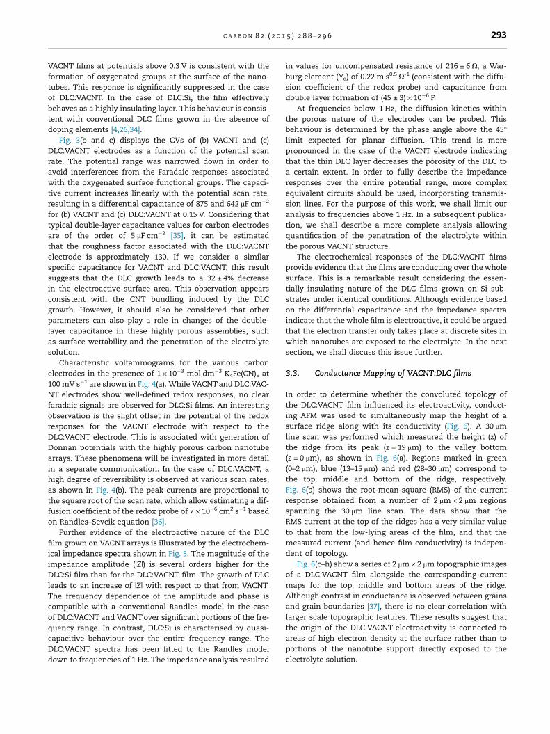
In order to determine whether the convoluted topology of
the DLC:VACNT film influenced its electroactivity, conduct-
ing AFM was used to simultaneously map the height of a
surface ridge along with its conductivity (Fig. 6). A 30 lm
line scan was performed which measured the height (z) of
the ridge from its peak (z = 19 lm) to the valley bottom
(z = 0 lm), as shown in Fig. 6(a). Regions marked in green
(0–2 lm), blue (13–15 lm) and red (28–30 lm) correspond to
the top, middle and bottom of the ridge, respectively.
Fig. 6(b) shows the root-mean-square (RMS) of the current
response obtained from a number of 2 lm · 2 lm regions
spanning the 30 lm line scan. The data show that the
RMS current at the top of the ridges has a very similar value
to that from the low-lying areas of the film, and that the
measured current (and hence film conductivity) is indepen-
dent of topology.
Fig. 6(c–h) show a series of 2 lm · 2 lm topographic images
of a DLC:VACNT film alongside the corresponding current
maps for the top, middle and bottom areas of the ridge.
Although contrast in conductance is observed between grains
and grain boundaries [37], there is no clear correlation with
larger scale topographic features. These results suggest that
the origin of the DLC:VACNT electroactivity is connected to
areas of high electron density at the surface rather than to
portions of the nanotube support directly exposed to the
electrolyte solution.
Fig. 6 – Conducting AFM measurements of the topography and current taken over a 2 · 30 lm scan region extending from the
base to the peak of a ridge structure in a DLC:VACNT film. 2 · 2 lm scans were collected incrementally with an applied tip-
sample bias of 100 mV. (a) Topographic data for the central line of each 2 · 2 lm scan combined to produce a single
continuous line scan, displayed as vertical height, z, over a height of 19 lm. Regions defined as the ‘top’, ‘middle’ and
‘bottom’ of the ridge are outlined using green, blue and red dashed lines, respectively. (b) Total RMS current measured across
each 2 · 2 lm scan; the red line at 5.2 pA represents the average current across the whole 2 · 30 lm region with an average
RMS error of 39%. The lower 6 images are three-dimensional representations of the topography and current measured at the
three different positions on the ridge: (c and f) top of the ridge (green dashed lines), (d and g) middle of the ridge (blue dashed
lines), (e and h) base of the ridge (red dashed lines). (A colour version of this figure can be viewed online.)
294 C A R B O N 8 2 ( 2 0 1 5 ) 2 8 8 – 2 9 6
C A R B O N 8 2 ( 2 0 1 5 ) 2 8 8 – 2 9 6 295
4. Conclusions
The present work demonstrates for the first time that electro-
active DLC films can be grown on VACNT arrays by PECVD
without the introduction of dopants. Such highly corrugated
DLC:VACNT films show web-like structures and ridges across
the surface, and behave as conducting, high-surface-area,
robust, all-carbon electrodes. The topography and electroac-
tivity of DLC:VACNT films are in stark contrast with the
smooth and insulating characteristics of DLC films grown
on Si wafers under identical conditions. Cyclic voltammetry
and impedance spectroscopy in the presence of ferrocyanide
as a redox probe exhibit reversible behaviour with a differen-
tial capacitance above 0.6 mF cm�2. Analysis of the topo-
graphic and conductance images demonstrated that the film
electroactivity is not linked to specific topographic features.
SEM data show that the DLC thickness is �25 nm, excluding
the possibility of direct tunnelling of electrons across this
DLC layer. It could be argued that electronic states in the
CNT arrays overlap with the electronic bands of the DLC layer,
creating a quasi-degenerate DLC film. This would be consis-
tent with the Raman measurements which showed that the
DLC:VACNT films had a reduced band gap compared to
DLC alone. To further advance our understanding of this
complex composite material, high resolution mapping of
electrochemical activity should be recorded. In this sense,
novel approaches such as Scanning Electrochemical Cell
microscopy would be very valuable [38].
Acknowledgements
The electron microscopy work was performed with JEOL 6330
microscope at University of Bristol and with a HRSEM (FEI-
Inspect) microscope at the LME/LNLS-Campinas. We also
gratefully acknowledge CNPq (202439/2012-7), Fapesp (2014/
02163-7) and EPSRC (EP/K007025/1) for financial support.
R E F E R E N C E S
[1] Robertson J. Diamond-like amorphous carbon. MaterialsScience & Engineering R-Reports. 2002;37(4–6):129–281.
[2] Bewilogua K, Cooper CV, Specht C, Schroder J, Wittorf R,Grischke M. Effect of target material on deposition andproperties of metal-containing DLC (Me-DLC) coatings (vol127, pg 224, 2000). Surf Coat Technol 2000;132(2–3):275–83.
[3] de Castro Costa RP, Marciano FR, Lima Oliveira DA, Trava-Airoldi VJ. Enhanced DLC wear performance by the presenceof lubricant additives. Materials Research-Ibero-American. JMater 2011;14(2):222–6.
[4] Zeng A, Neto VF, Gracio JJ, Fan QH. Diamond-like carbon (DLC)films as electrochemical electrodes. Diam Relat Mater2014;43:12–22.
[5] Omer AMM, Adhikari S, Adhikary S, Rusop M, Uchida H, SogaT, et al. Electrical conductivity improvement by iodinedoping for diamond-like carbon thin-films deposited bymicrowave surface wave plasma CVD. Diam Relat Mater2006;15(4–8):645–8.
[6] Adhikary S, Tian XM, Adhikari S, Omer AMM, Uchida H,Umeno M. Bonding defects and optical band gaps of DLCfilms deposited by microwave surface-wave plasma CVD.Diam Relat Mater 2005;14(11–12):1832–4.
[7] Choi J, Nakao S, Kim J, Ikeyama M, Kato T. Corrosionprotection of DLC coatings on magnesium alloy. Diam RelatMater 2007;16(4–7):1361–4.
[8] Chen CW, Robertson J. Doping mechanism in tetrahedralamorphous carbon. Carbon 1999;37(5):839–42.
[9] Compton RG, Foord JS, Marken F. Electroanalysis at diamond-like and doped-diamond electrodes. Electroanalysis2003;15(17):1349–63.
[10] Hayashi Y, Ishikawa S, Soga T, Umeno M, Jimbo I.Photovoltaic characteristics of boron-doped hydrogenatedamorphous carbon on n-Si substrate prepared by rf plasma-enhanced CVD using trimethylboron. Diam Relat Mater2003;12(3–7):687–90.
[11] Rusop M, Mominuzzaman SM, Soga T, Jimbo T, Umeno M.Characterization of phosphorus-doped amorphous carbonand construction of n-carbon/p-silicon heterojunction solarcells. Jpn J Appl Phys 2003;42(4B):2339–44.
[12] Veerasamy VS, Amaratunga GAJ, Davis CA, Timbs AE, MilneWI, McKenzie DR. N-type doping of highly tetrahedraldiamond-like amorphous-carbon. J Phys 1993;5(13):L169–74.
[13] Liu LX, Liu E. Nitrogenated diamond-like carbon films formetal tracing. Surf Coat Technol 2005;198(1–3):189–93.
[14] Liu E, Kwek HW. Electrochemical performance of diamond-like carbon thin films. Thin Solid Films 2008;516(16):5201–5.
[15] Maalouf R, Chebib H, Saikali Y, Vittori O, Sigaud M, Garrelie F,et al. Characterization of different diamond-like carbonelectrodes for biosensor design. Talanta 2007;72(1):310–4.
[16] Kim J-I, Bordeanu A, Pyun J-C. Diamond-like carbon (DLC)microelectrode for electrochemical ELISA. BiosensBioelectron 2009;24(5):1394–8.
[17] Schnupp R, Kuhnhold R, Temmel G, Burte E, Ryssel H. Thincarbon films as electrodes for bioelectronic applications.Biosens Bioelectron 1998;13(7–8):889–94.
[18] Hu H, Chen G, Zha J. Facile synthesis of CNTs-dopeddiamond-like carbon film by electrodeposition. Surf CoatTechnol 2008;202(24):5943–6.
[19] Wei C, Wang C-I, Tai F-C, Ting K, Chang R-C. The effect ofCNT content on the surface and mechanical properties ofCNTs doped diamond like carbon films. Diam Relat Mater2010;19(5–6):562–6.
[20] Kinoshita H, Ippei I, Sakai H, Ohmae N. Synthesis andmechanical properties carbon nanotube/diamond-likecarbon composite films. Diam Relat Mater 2007;16(11):1940–4.
[21] Wei C, Yang J-F. A finite element study on the hardness ofcarbon nanotubes-doped diamond-like carbon film. J MaterRes 2012;27(1):330–8.
[22] Kinoshita H, Ippei I, Sakai H, Ohmae N. Synthesis andmechanical properties carbon nanotube/diamond-likecarbon composite films. Diam Relat Mater 2007;11:1940–4.
[23] Zanin H, May PW, Hamanaka MHMO, Corat EJ. Field emissionfrom hybrid diamond-like carbon and carbon nanotubecomposite structures. ACS Appl Mater Interf2013;5(23):12238–43.
[24] Zanin H, May PW, Fermin DJ, Plana D, Vieira SMC, Milne WI,et al. Porous boron-doped diamond/carbon nanotubeelectrodes ACS. Acs Appl Mater Interf 2014;6(2):990–5.
[25] Lobo AO, Ramos SC, Antunes EF, Marciano FR, Trava-AiroldiVJ, Corat EJ. Fast functionalization of vertically alignedmultiwalled carbon nanotubes using oxygen plasma. MaterLett 2012;70:89–93.
[26] Zanin HG, May PW, Lobo AO, Saito E, Machado JPB, Martins G,et al. J Electrochem Soc 2014;161(5):H290–5.
296 C A R B O N 8 2 ( 2 0 1 5 ) 2 8 8 – 2 9 6
[27] Ferrari AC, Robertson J. Interpretation of Raman spectra ofdisordered and amorphous carbon. Phys Rev B 2000;61:14095–107.
[28] Zanin H, Margraf-Ferreira A, da Silva NS, Marciano FR, CoratEJ, Lobo AO. Graphene and carbon nanotube compositeenabling a new prospective treatment for trichomoniasisdisease. Mater Sci Eng C 2014;41:65–9.
[29] Zanin H, Saito E, Marciano FR, Ceragioli HJ, Granato AEC,Porcionatto M, Lobo AO. Fast preparation of nano-hydroxyapatite/superhydrophilic reduced graphene oxidecomposites for bioactive applications. J Mater Chem B2013;1(38):4947–55.
[30] Irmer G, Dorner-Reisel A. Micro-Raman studies on DLCcoatings. Adv Eng Mater 2005;7(8):694–705.
[31] Ferrari AC, Robertson J. Raman spectroscopy of amorphous,nanostructured, diamond-like carbon, and nanodiamond.Philos Transact R Soc 1824;2004(362):2477–512.
[32] Tamor MA, Vassell WC. Raman fingerprinting of amorphous-carbon films. J Appl Phys 1994;76(6):3823–30.
[33] Ferrari AC, Robertson J. Interpretation of Raman spectra ofdisordered and amorphous carbon. Phys Rev B 2000;61(20).
[34] Papakonstantinou P, Zhao JF, Lemoine P, McAdams ET,McLaughlin JA. The effects of Si incorporation on the
electrochemical and nanomechanical properties of DLC thinfilms. Diam Relat Mater 2002;11(3–6):1074–80.
[35] Bradbury CR, Kuster L, Fermin DJ. Electrochemical reactivityof HOPG electrodes modified by ultrathin films and two-dimensional arrays of metal nanoparticles. J ElectroanalChem 2010;646(1–2):114–23.
[36] Silva TA, Zanin H, Saito E, Medeiros RA, Vicentini FC, Corat EJ,et al. Electrochemical behaviour of vertically aligned carbonnanotubes and graphene oxide nanocomposite as electrodematerial. Electrochim Acta 2014;119:114–9.
[37] Chatterjee V, Harniman R, May PW, Barhai PK. Directobservation of electron emission from the grain boundariesof chemical vapour deposition diamond films by tunnellingatomic force microscopy. Appl Phys Lett 2014;104:171907.
[38] Snowden ME, Guell AG, Lai SCS, McKelvey K, Ebejer N,O’Connell MA, et al. Scanning electrochemical cellmicroscopy: theory and experiment for quantitative highresolution spatially-resolved voltammetry and simultaneousion-conductance measurements. Anal Chem2012;84(5):2483–91.