Embed Size (px)
Citation preview

HighHigh StepStep--up Ratio DCup Ratio DC--DC DC Converter TopologiesConverter Topologies
P. P. TentiTenti, L. , L. RossettoRossetto, G. , G. SpiazziSpiazzi, S. , S. BusoBuso, P. , P. MattavelliMattavelli, , L. L. CorradiniCorradini
Dept. of Information Engineering Dept. of Information Engineering –– DEIDEIUniversity of PadovaUniversity of Padova
Speaker: G. Speaker: G. SpiazziSpiazzi
Part IPart I

2
Seminar OutlineSeminar Outline
• Why we need high step-up ratio converters?– Application fields
• Low power high step-up ratio topologies– Coupled inductors
• High power high step-up ratio topologies– Non isolated
– Isolated

3
High StepHigh Step--up Ratio Topologiesup Ratio Topologies
• Low-voltage high-current energy sources– Fuel-cells (some kW)
– Paralleled photovoltaic modules in domestic applications (some kW)
– Microinverter, i.e. connection of a single photovoltaic module to the grid (some hundred watts)
• Step-down inverters require an input voltage higher than the maximum line voltage peak
Why?Why?

4
Example of Example of MicroinverterMicroinverter
• Modularity• Reduction of partial shading effects• Dedicated Maximum Power Point Tracker (MPPT)
200-300W single pv panel
Utility
grid
High Step-Up
DC-DC
Microinverterfor single panel
MicroinverterMicroinverterstructurestructure

5
Simple Boost TopologySimple Boost Topology
( )( )
( )oo
o
D2
o
LSDR,U,dF
d11
UU
d1R
rdrd1r1
1d1
1M ⋅
−=
+−
++−+−=
Switch model
L
C
D
S
+
Ui Uo
+
-
Io+UDIL
Ro
rD
rS
rL
Diode model
Boost scheme including some parasitic elements:Boost scheme including some parasitic elements:
Voltage Voltage conversion ratio conversion ratio (neglecting inductor
current ripple):

6
Simple Boost TopologySimple Boost Topology
0 0.1 0.2 0.3 0.4 0.5 0.6 0.7 0.8 0.9 10
2
4
6
8
Duty-cycle
M
Ro
ideal
Voltage conversion ratio Voltage conversion ratio MM including including conduction losses:conduction losses:
Mmax

7
Simple Boost TopologySimple Boost Topology
Converter Converter efficiency:efficiency:
0 0.1 0.2 0.3 0.4 0.5 0.6 0.7 0.8 0.9 10.7
0.75
0.8
0.85
0.9
0.95
1ηηηη
Ro
Duty-cycle
( ) ( )ooLi
Do
ii
oo
in
out R,U,dFd1MIUIU
IUIU
PP =−====η

8
Low Power Applications Low Power Applications
Ug
U1
U2
+
+
D2
D1S
1:n21
ig
Ld
Lmim
Uo
+
-C1
C2
•• ExampleExample: integrated Boost-Flyback converter
It can be seen as a flyback converter with a non dissipative snubber: D1 and C1 deliver to the output the energy stored
in the transformer leakage inductance Ld
9
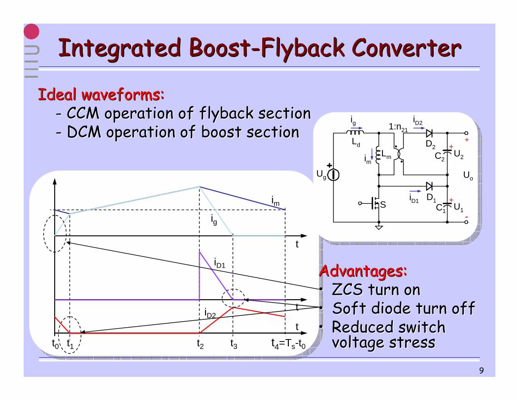
Integrated BoostIntegrated Boost--FlybackFlyback ConverterConverter
Ideal waveforms:Ideal waveforms:-- CCM operation of CCM operation of flybackflyback sectionsection-- DCM operation of boost sectionDCM operation of boost section
ig
im
iD1
iD2
t
t
t
t0 t1 t2 t3 t4=Ts-t0
Ug
U1
U2
+
+
D2
D1S
1:n21
ig
Ld
Lmim
Uo
+
-C1
C2
iD2
iD1
Advantages:Advantages:•• ZCS turn on ZCS turn on •• Soft diode turn offSoft diode turn off•• Reduced switch Reduced switch voltage stressvoltage stress

10
Integrated BoostIntegrated Boost--FlybackFlyback ConverterConverter
Problems:Problems:
Parasitic oscillations at DParasitic oscillations at D22 turn off caused by its turn off caused by its capacitance Ccapacitance Crr resonating with transformer leakage resonating with transformer leakage inductances Linductances Ldd and Land Lss
High voltage stress across D2Ug
U1
U2
+
+
D2
D1S
1:n21
ig
Ld
Lmim
Uo
+
-
Ls
is
C1
C2
ur+
Cr
Dissipative R-C-D snubberis needed

11
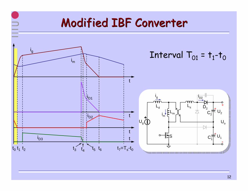
Modified IBF ConverterModified IBF Converter
Clamping diode D3 added to the original topology
Advantages:Advantages:•• Clean diode voltage Clean diode voltage waveforms without parasitic waveforms without parasitic oscillationsoscillations
•• Energy transfer toward the Energy transfer toward the output also during switch turn output also during switch turn on intervalon interval
•• Slight voltage gain increase Slight voltage gain increase due to resonances between due to resonances between parasitic componentsparasitic components
Ug
U1
U2
+
+
D2
D1
D3
S
1:n21
ig
Ld
Lmim
Uo
+
-
Ls
is
C1
C2
ur+
Cr
x
12
Modified IBF ConverterModified IBF Converter
Interval T01 = t1-t0ig
im
iD1
iD2
iD3
t
t
tt
t0 t1 t3 t4 t6 t7=Ts-t0t2 t5
Ug
U1
U2
+
+
D2
S
ig
Ld
Lmim
Uo
+
-
Ls
C1
C2
iD2

13
Modified IBF ConverterModified IBF Converter
Interval T12 = t2-t1ig
im
iD1
iD2
iD3
t
t
tt
t0 t1 t3 t4 t6 t7=Ts-t0t2 t5
Ug
U1
U2
+
+S
ig
Ld
Lmim
Uo
+Ls
C1
C2
ur+
Cr
-
14
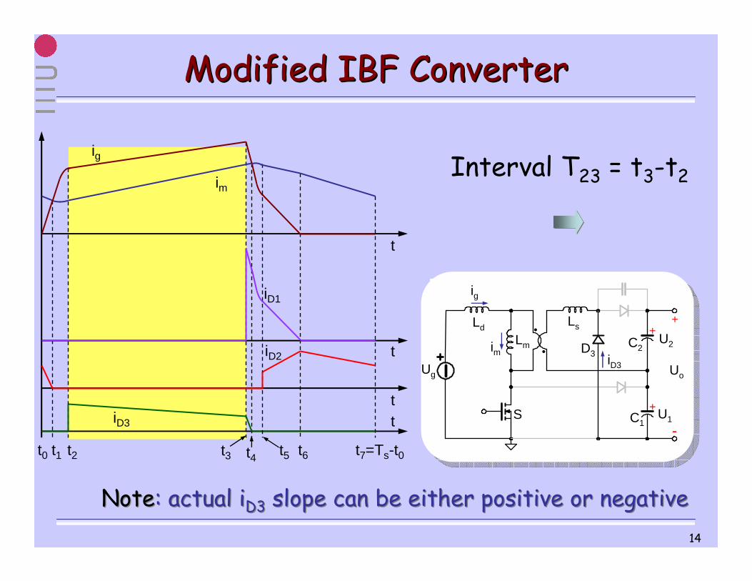
Modified IBF ConverterModified IBF Converter
Interval T23 = t3-t2ig
im
iD1
iD2
iD3
t
t
tt
t0 t1 t3 t4 t6 t7=Ts-t0t2 t5
Note: actual iD3 slope can be either positive or negativeNote: actual iD3 slope can be either positive or negative
Ug
U1
U2
+
+
D3
S
ig
Ld
Lmim
Uo
+Ls
iD3
C1
C2
-

15
Modified IBF ConverterModified IBF Converter
Interval T34 = t4-t3ig
im
iD1
iD2
iD3
t
t
tt
t0 t1 t3 t4 t6 t7=Ts-t0t2 t5
Ug
U1
U2
+
+D1
D3
S
ig
Ld
Lmim
Uo
+Ls
iD1
C1
C2
-
iD3

16
Modified IBF ConverterModified IBF Converter
Interval T45 = t5-t4ig
im
iD1
iD2
iD3
t
t
tt
t0 t1 t3 t4 t6 t7=Ts-t0t2 t5
Ug
U1
U2
+
+D1
ig
Ld
Lmim
Uo
+Ls
C1
C2
-
ur+
Cr
iD1
17
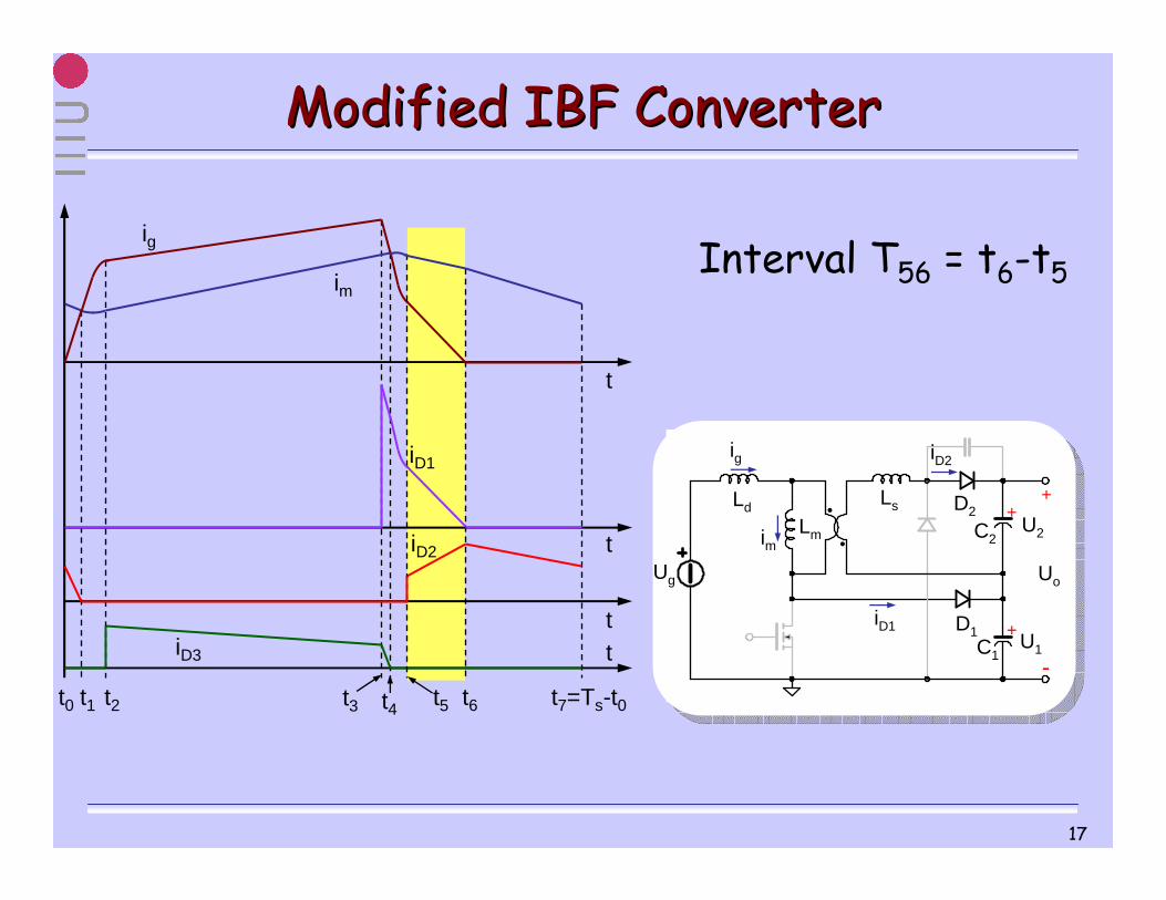
Modified IBF ConverterModified IBF Converter
Interval T56 = t6-t5ig
im
iD1
iD2
iD3
t
t
tt
t0 t1 t3 t4 t6 t7=Ts-t0t2 t5
Ug
U1
U2
+
+
D2
D1
ig
Ld
Lmim
Uo
+Ls
C1
C2
-
iD1
iD2

18
Modified IBF ConverterModified IBF Converter
Interval T67 = t7-t6ig
im
iD1
iD2
iD3
t
t
tt
t0 t1 t3 t4 t6 t7=Ts-t0t2 t5
U1
U2
+
+
D2Lmim
Uo
+Ls
C1
C2
-
iD2

19
Converter ParametersConverter Parameters
• Input voltage: Ug = 25-35 V
• Output voltage: Uo = 400 V
• Nominal output power: Po = 300 W
• Switching frequency: fs = 100 kHz
• Magnetizing inductance: Lm = 20 µH
• Primary leakage inductance: Ld = 0.4 µH
• Secondary leakage inductance: Ls = 2 µH

20
Voltage Conversion RatioVoltage Conversion Ratio
5
9
13
17
21
0.4 0.5 0.6 0.7 0.8
M
4
4.4
4.8
5.2
5.6M1
Duty-cycle
g
o
U
UM =
g
11 U
UM =
Comparison between calculations and spice simulations
This unmatched point corresponds to a
different topological sequence

21
Voltage Conversion RatioVoltage Conversion Ratio
g
o
U
UM =
Effect of resonant intervals on the overall voltage gain
0.4 0.45 0.5 0.55 0.6 0.65 0.76
7
8
9
10
11
12
13
14M
Duty-cycle
No parasitic components
With parasitic components

22
Experimental ResultsExperimental Results
Ug = 35 V, Uo = 400 V, Po = 300 W
ig [2.5A/div]
uDS [50V/div
ux [100V/div]
Peaking due to a small dip in the converter input voltage due to fast current rise time

23
Experimental ResultsExperimental Results
Ug = 35 V, Uo = 400 V, Po = 300 W
ig
im
iD1
iD2
iD3
t
t
tt
t0 t1 t3 t4 t6 t7=Ts-t0
Impk
t2 t5
t0 t1 t2
ig
uDS
ux
t3t4 t5
ig
uDS
ux
t6

24
Experimental ResultsExperimental Results
Ug = 25 V, Uo = 400 V, Po = 300 W
t0 t1 t2 t3
ig [5A/div]
uDS [50V/div
ux [100V/div]
Ug
U1
U2
+
+
D3
S
ig
Ld
Lmim
Uo
+Ls
iD3
C1
C2
-
D3 turns off during the switch on interval

25
Measured EfficiencyMeasured Efficiency
Po = 300 W
0.92
0.93
0.94
0.95
25 27 29 31 33 35Ug [V]
ηfs = 100kHz
fs = 200kHz
0.90
0.91
0.92
0.93
0.94
25 27 29 31 33 35Ug [V]
η
fs = 200kHz
fs = 100kHz
Po = 200 W

26
Measured EfficiencyMeasured Efficiency
0.92
0.93
0.94
0.95
300250200150100Po [W]
ηUg = 35V
Ug = 25V
fs = 100 kHz

27
IBF Converter with Voltage MultiplierIBF Converter with Voltage Multiplier
Ug U1
U2
+
+D2
D1
D3
S
ig
Ld Lm
im
Uo
+
-C1
C2
+C3 U3
Voltage multiplier cell

28
IBF Converter with Voltage MultiplierIBF Converter with Voltage Multiplier
Ug
U1
U2
+
+
D2
D1
D3
S
1:n21
ig
Ld
Lmim
Uo
+
-
Ls
is
C1
C2
ur+
Cr
x
Ug U1
U2
+
+D2
D1
D3
S
ig
Ld Lm
im
Uo
+
-C1
C2
+C3 U3
IBF converter with voltage multiplier cellIBF converter with voltage multiplier cellversus versus modified IBFmodified IBF
Similar behavior with a Similar behavior with a higher degree of freedomhigher degree of freedomin controlling the switch voltage stressin controlling the switch voltage stress
X

29
Converter WaveformsConverter Waveforms
BOOST section in BOOST section in DCMDCM and FLYBACK section inand FLYBACK section in CCMCCM
Ug U1
U3
+
+
D3
D1
D2
S
Np
Uo
+
-C1
C3
U2
+C2
Ns
Ld Lm
ig im
is
Cr
Ls
+ur
x
ig
im
iD1
iD2
iD3
t
t
tt
t0 t1 t3 t4 t6 t7=Ts-t0
ImpkIm1
Im2Imvl
Im1/n21
Im2/n21
Impk
t2 t5
Igpk
-is(t2)
is(t5)
iD3(t3)

30
5
10
15
20
25
0.4 0.5 0.6 0.7 0.81
2
3
4
5
Duty-cycle
M M1
Experimental PrototypeExperimental PrototypeDesign exampleDesign example:
Input voltage:Ug = 25÷35VOutput voltage: Uo = 400VNominal output power: Po = 300WSwitching frequency: fs = 100kHzBoost output: U1 = 75V Magnetizing inductance:Lm = 20µHPrimary leakage inductance:Ld = 0.4µHSecondary leakage inductance:Ls = 2µH
From the design constraints:
M= Uo / Ug=400/35=11.42 M1= U 1/ Ug=75/35=2.143
Numerically solving:
d = 0.519, n21 = 4.589 M2 = U 2/ Ug = 4.823 M3 = M-M1-M2 = U 3/ Ug = 4.454
Based on desired current ripple and DCM-CCM mode at nominal power
150V rated mosfet calculated voltage gains (continuous
curves) and simulation results (dotted)

31
Experimental resultsExperimental results
ig
uDS
ux
t0 t1 t2
ig
uDS
ux
t0 t1 t2
ig
uDS
ux
t3 t4 t5
ig
uDS
ux
t6
ux: 100V/div; uDS: 20V/div; ig: 5A/div
Measured main waveforms in a switching period Ug = 35V, Vo = 400V, Po = 300W
Details of turn on and turn off intervals
Ug U1
U3
+
+
D3
D1
D2
S
Np
Uo
+
-C1
C3
U2
+C2
Ns
Ld Lm
ig im
is
Cr
Ls
+ur
x
zero current turn on
layout stray
inductances resonance

32
Converter efficiencyConverter efficiency
Fig.1 Fig.2
Efficiency Efficiency
The converter efficiency was measured as a function of input voltage, at Po=300W,Fig.1, and at Ug=[25V,35V] and variable
output power, Fig. 2
25 27 29 31 33 35Ug [V]
0.93
0.94
0.95
η
0.93
0.94
0.95
0.96Ug = 35V
Ug = 25V
300250200150100Po [W]
η

33
Isolated IBF ConverterIsolated IBF Converter
Ug
U1
ur
+
+
SAC
D1
D2
Np
Uo
+
-
C1
Cr U2
+C2
Ns
Ld
Lm
ig
imis
id
S
CAC+
io
LsRo
UAC
Ug U1
U3
+
+
D3
D1
D2
S
Np
Uo
+
-C1
C3
U2
+C2
Ns
Ld Lm
ig im
is
Cr
Ls
+ur
x
For For isolationisolation, the loss, the loss--less less snubbersnubber DD11--CC11 is is substituted by an substituted by an
active clampactive clamp

34
Isolated IBF ConverterIsolated IBF Converter
Advantages:Advantages:
•• ZVS turn on ZVS turn on
•• Soft diode turn offSoft diode turn off
•• Reduces switch voltage stressReduces switch voltage stress
•• Clean diode voltage waveforms without parasitic Clean diode voltage waveforms without parasitic oscillationsoscillations
•• Energy transfer toward the output also during Energy transfer toward the output also during switch turn on intervalswitch turn on interval
•• Reduced active clamp circulating currentReduced active clamp circulating current

35
Converter OperationConverter Operation
Interval T01 = t1-t0
id(t0)
Ug
idim
iSAC
iD2
iD1
t
t
t
tt0 t1 t3 t4 t6=Ts-t0
Impk
Imvl
t2 t5
im(t0)
Ug
U1
+
Np
Uo
+
-
C1
U2
+C2
Ns
Ld
Lm
ig
imis
id
S
io
LsRo
D2
Soft DSoft D22 turn offturn off
Hp: negligible capacitor voltage ripples

36
Converter OperationConverter Operation
Interval T12 = t2-t1
id(t0)
Ug
idim
iSAC
iD2
iD1
t
t
t
tt0 t1 t3 t4 t6=Ts-t0
Impk
Imvl
t2 t5
im(t0)
Ug
U1
ur
+
+
Np
Uo
+
-
C1
Cr U2
+C2
Ns
Ld
Lm
ig
imis
id
S
io
LsRo
Hp: negligible capacitor voltage ripples

37
Converter OperationConverter Operation
Interval T23 = t3-t2
Note: actual iD1 slope can be either positive or negativeNote: actual iD1 slope can be either positive or negative
id(t0)
Ug
idim
iSAC
iD2
iD1
t
t
t
tt0 t1 t3 t4 t6=Ts-t0
Impk
Imvl
t2 t5
im(t0)
Ug
U1
+D1
Np
Uo
+
-
C1
U2
+C2
Ns
Ld
Lm
ig
imis
id
S
io
LsRo
Hp: negligible capacitor voltage ripples

38
Converter OperationConverter Operation
Interval T34 = t4-t3
id(t0)
Ug
idim
iSAC
iD2
iD1
t
t
t
tt0 t1 t3 t4 t6=Ts-t0
Impk
Imvl
t2 t5
im(t0)
U1
+
SAC
D1
Np
Uo
+
-
C1
U2
+C2
Ns
Ld
Lmim
is
id
CAC+
io
LsRo
UAC
Soft DSoft D11 turn offturn off
Hp: negligible capacitor voltage ripples

39
Converter OperationConverter Operation
Interval T45 = t5-t4
id(t0)
Ug
idim
iSAC
iD2
iD1
t
t
t
tt0 t1 t3 t4 t6=Ts-t0
Impk
Imvl
t2 t5
im(t0)
U1
ur
+
+
SAC
Np
Uo
+
-
C1
Cr U2
+C2
Ns
Ld
Lmim
is
id
CAC+
io
LsRo
UAC
Reduced active clamp circulating currentReduced active clamp circulating current
Hp: negligible capacitor voltage ripples

40
Converter OperationConverter Operation
id(t0)
Ug
idim
iSAC
iD2
iD1
t
t
t
tt0 t1 t3 t4 t6=Ts-t0
Impk
Imvl
t2 t5
im(t0)
Hp: negligible capacitor voltage ripples
Interval T56 = t6-t5
U1
+
SAC
D2
Np
Uo
+
-
C1
U2
+C2
Ns
Ld
Lmim
is
id
CAC+
io
LsRo
UAC

41
Converter ParametersConverter Parameters
• Input voltage: Ug = 25-35 V
• Output voltage: Uo = 400 V
• Nominal output power: Po = 300 W
• Switching frequency: fs = 100 kHz
• Magnetizing inductance: Lm = 20 µH
• Primary leakage inductance: Ld = 0.4 µH
• Secondary leakage inductance:Ls = 2 µH

42
id [5A/div]
uDS [20V/div]
uD1 [100V/div]
Experimental ResultsExperimental Results
Ug = 35 V, Uo = 400 V, Po = 300 W (2µs/div)
Peaking due to a small dip in the converter input voltage due to the fast current rise time

43
id [5A/div]
uDS [20V/div]
uD1 [100V/div]
Experimental ResultsExperimental Results
Ug = 35 V, Uo = 400 V, Po = 300 W (2µs/div)
The resonant phase reduces the active clamp
circulating current}

44
id [5A/div]
Experimental ResultsExperimental Results
Ug = 35 V, Uo = 400 V, Po = 300 W (2µs/div)
The resonant phase reduces the active clamp
circulating current}
Ug
ur
+
+
SAC
D1
D2
Uo
+
-
C1
Cr
+C2
Ld
Lm
S
CAC+Ls
Ro
UAC
390 pF external capacitor added

45
Detail of Main Switch Turn OnDetail of Main Switch Turn On
Ug = 35 V, Uo = 400 V, Po = 300 W
id(t0)
Ug
idim
iSAC
iD2
iD1
t
t
t
tt0 t1 t3 t4 t6=Ts-t0
Impk
Imvl
t2 t5
im(t0)
t6 = t0 t1 t2
id [5A/div]
uDS [20V/div]
uD1 [100V/div]
Time scale: 500ns/div

46
Detail of Main Switch Turn OffDetail of Main Switch Turn Off
Ug = 35 V, Uo = 400 V, Po = 300 W
id(t0)
Ug
idim
iSAC
iD2
iD1
t
t
t
tt0 t1 t3 t4 t6=Ts-t0
Impk
Imvl
t2 t5
im(t0)
t3t4 t5
id [5A/div]
uDS [20V/div]
uD1 [100V/div]
Time scale: 500ns/div

47
Zero Voltage Switching Zero Voltage Switching
id [5A/div]
uDS [20V/div]
uD1 [100V/div]
uGS [5V/div]
Detail of the main switch turn on (nominal output power)
[200ns/div]

48
Different Operating ModeDifferent Operating Mode
Ug = 25 V, Uo = 400 V, Po = 100 W
D1 turns off during the switch on interval
id [2A/div]
uDS [20V/div]
uD1 [100V/div]
U1
+
D2
Uo
+
-
C1
U2
+C2
Ld
Lmim
id io
Ro
D1

49
Measured EfficiencyMeasured Efficiency
Po = 300 W
0.91
0.92
0.93
0.94
25 27 29 31 33 35Ug [V]
η
0.92
0.93
0.94
0.95
300250200150100
ηUg = 35V
Ug = 25V
Po [W]
Power stage only

50
CommentsComments
• There are different topologies presented in literature whose behavior is very similar to the Integrated Boost-Flyback converter.
• These topologies have a drawback of a discontinuous input current waveform, that make the use of such converters for higher power levels at least problematic.
• For high power applications, a continuous input current represents a very nice feature


![HIGH-CONVERSION-RATIO BIDIRECTIONAL DC–DC ......bidirectional dc –dc converter with a high convention ratio is a key component of battery applications [5] Isolated bidirectional](https://img.pdfslide.us/doc/110x75/5f0a32787e708231d42a7b2d/high-conversion-ratio-bidirectional-dcadc-bidirectional-dc-adc-converter.jpg)