Embed Size (px)
Citation preview
MCP1631/HV/MCP1631V/VHVHigh-Speed, Pulse Width Modulator
Features• Programmable Switching Battery Charger
Designs• High-Speed Analog PWM Controller
(2 MHz Operation)• Combine with Microcontroller for “Intelligent”
Power System Development• Peak Current Mode Control (MCP1631)• Voltage Mode Control (MCP1631V)• High Voltage Options Operate to +16V Input:
- MCP1631HV Current Mode- MCP1631VHV Voltage Mode
• Regulated Output Voltage Options:- +5.0V or +3.3V- 250 mA maximum current
• External Oscillator Input sets Switching Frequency and Maximum Duty Cycle Limit
• External Reference Input Sets Regulation Voltage or Current
• Error Amplifier, Battery Current ISNS Amplifier, Battery Voltage VSNS Amplifier Integrated
• Integrated Overvoltage Comparator• Integrated High Current Low Side MOSFET
Driver (1A Peak)• Shutdown mode reduces IQ to 2.4 µA (typical)• Internal Overtemperature Protection• Undervoltage Lockout (UVLO)• Package Options:
- 4 mm x 4 mm 20-Lead QFN(MCP1631/MCP1631V only)
- 20-Lead TSSOP (All Devices)- 20-Lead SSOP (All Devices)
Applications• High Input Voltage Programmable Switching
Battery Chargers• Supports Multiple Chemistries Li-Ion, NiMH, NiCd
Intelligent and Pb-Acid • LED Lighting Applications• Constant Current SEPIC Power Train Design• USB Input Programmable Switching Battery
Chargers
General DescriptionThe MCP1631/MCP1631V is a high-speedanalog pulse width modulator (PWM) used to developintelligent power systems. When combined with amicrocontroller, the MCP1631/MCP1631V will controlthe power system duty cycle providing output voltageor current regulation. The microcontroller can be usedto adjust output voltage or current, switching frequencyand maximum duty cycle while providing additionalfeatures making the power system more intelligent,robust and adaptable.
Typical applications for the MCP1631/MCP1631Vinclude programmable switch mode battery chargerscapable of charging multiple chemistries, like Li-Ion,NiMH, NiCd and Pb-Acid configured as single ormu l t ip le ce l l s . By combin ing w i th a sma l lmicrocontroller, intelligent LED lighting designs andprogrammable SEPIC topology voltage and currentsources can also be developed.
The MCP1631/MCP1631V inputs were developed tobe attached to the I/O pins of a microcontroller fordesign flexibility. Additional features integrated into theMCP1631HV/MCP1631VHV provide signal condition-ing and protection features for battery charger orconstant current source applications.
For applications that operate from a high voltage input,the MCP1631HV and MCP1631VHV device optionscan be used to operate directly from a +3.5V to +16Vinput. For these applications, an additional low drop out+5V or +3.3V regulated output is available and canprovide current up to 250 mA to power a microcontrollerand auxiliary circuits.
© 2008 Microchip Technology Inc. DS22063B-page 1
MCP1631/HV/MCP1631V/VHV
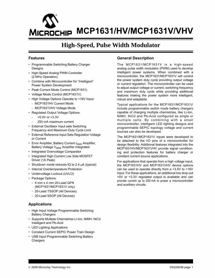
Package Types
1
2
3
COMP
PGND
4
5
6
7
8
9
10
20
19
18
17
16
15
14
13
12
11
20-Lead SSOP and TSSOPMCP1631/MCP1631V
SHDN
OSCIN
OSCDIS
OVIN
VREF
AGND
NC
NC
NC AVDD_IN
VSIN
ISIN
VSOUT
ISOUT
FB
CS/VRAMP
PVDD
VEXT 1
2
3
COMP
PGND
4
5
6
7
8
9
10
20
19
18
17
16
15
14
13
12
11
20-Lead SSOP and TSSOPMCP1631HV/MCP1631VHV
SHDN
OSCIN
OSCDIS
OVIN
VREF
AGND
NC
NC
AVDD_OUT
VSIN
ISIN
VSOUT
ISOUT
FB
CS/VRAMP
PVDD
VEXT
VIN
CO
MP
PGND
SH
DN
AGND
NC
NC
VSIN
ISIN
VS
OU
T
ISO
UT
FB
CS/VRAMP
PVDD
VEXT
AVDD_IN
1
2
3
4
5
6 7 8 9 10
15
14
13
12
11
20 19 1 8 17 16
NC
OS
CIN
OS
CD
IS
OV
IN
VR
EF
EP
20 Lead 4x4 QFNMCP1631/MCP1631V
21
DS22063B-page 2 © 2008 Microchip Technology Inc.
MCP1631/HV/MCP1631V/VHV
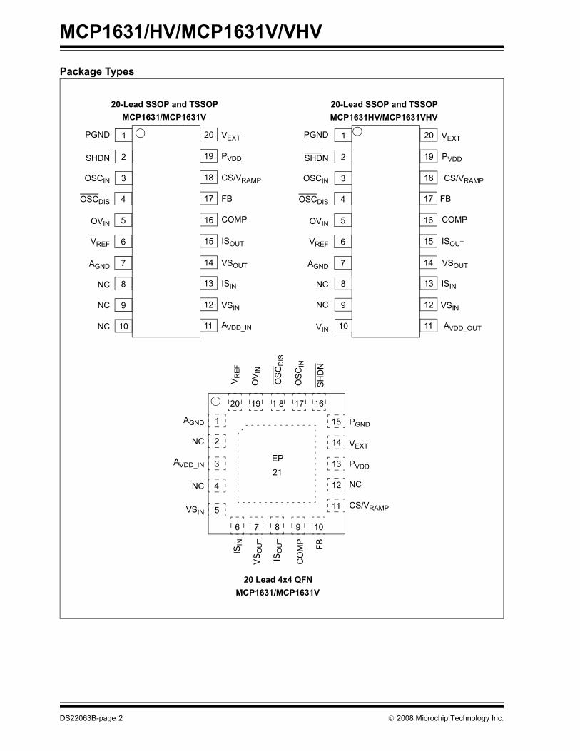
Typical Application Diagram
COMP
PGND
SHDN
OSCIN
OSCDIS
OVIN
VREF
AGND
NC
NC
AVDD_OUT
VSIN
ISIN
VSOUT
ISOUT
FB
CS
PVDD
VEXT
L1A
CIN
SCHOTTKYDIODE
COUT
L1B
CC
MCP1631HV
VIN
RTHERM
AVDD_OUT
GP0/C
C
GP5
GP3
GP1/C
PIC12F683
LED
R
GND
GP4
CCP1
VDD
VIN Range +5.5V to +16V
Multi-cell, Multi-Chemistry Charger
© 2008 Microchip Technology Inc. DS22063B-page 3
MCP1631/HV/MCP1631V/VHV
Functional Block Diagram(1)
MCP1631HV/VHV High Speed PIC PWM
R
S Q
Q
A1+
-VREF
FB
C1+
-
CS/VRAMP
OSCIN
PVDD
COMP
PGND
VEXT
2R
2.7V Clamp
OT
UVLO
100 kΩ
0.1 µA
VDD
R
+
- R
R
10R
+
-
A2
A3
+3.3V or +5.0V LDO 250 mA
VIN
AVDD_OUT / AVDD_IN
VDD
Shutdown ControlA3 Remains OnSHDN
ISIN
ISOUT
VSIN
VSOUT
C2+
-
VDD
AGND
OVIN
Overvoltage Compw/ Hysteresis
Internal1.2V VREF
OSCDIS
100 kΩ
Remove for MCP1631Vand MCP1631VHV Options
Internal Regulator for MCP1631HV and MCP1631VHVOptions Only; For MCP1631 and MCP1631V AVDD_IN is input
VDD
VDD
VDD
VDD
VDD
Note 1: For Shutdown control, amplifier A3 remains functional sobattery voltage can be sensed during discharge phase.
2: For HV options, internal Low Drop Out Regulator provides+3.3V or +5.0V bias to VDD.
DS22063B-page 4 © 2008 Microchip Technology Inc.
MCP1631/HV/MCP1631V/VHV
1.0 ELECTRICAL CHARACTERISTICS
Absolute Maximum Ratings †VIN - GND (MCP1631/V)................................................+6.5VVIN - GND (MCP1631HV/VHV)....................................+18.0VAll Other I/O ..............................(GND - 0.3V) to (VDD + 0.3V)LX to GND............................................. -0.3V to (VDD + 0.3V)VEXT Output Short Circuit Current ........................ContinuousStorage temperature .....................................-65°C to +150°CMaximum Junction Temperature...................-40°C to +150°COperating Junction Temperature...................-40°C to +125°CESD Protection On All Pins:HBM .................................................................................4 kVMM ..................................................................................400V
† Notice: Stresses above those listed under "MaximumRatings" may cause permanent damage to the device. This isa stress rating only and functional operation of the device atthose or any other conditions above those indicated in theoperational sections of this specification is not intended.Exposure to maximum rating conditions for extended periodsmay affect device reliability.
DC CHARACTERISTICSElectrical Specifications: Unless otherwise noted, VIN = 3.0V to 5.5V, FOSC = 1 MHz with 10% Duty Cycle, CIN = 0.1 µF,VDD for typical values = 5.0V, TA for typical values = +25°C, TA = -40°C to +125°C for all minimum and maximums.
Parameters Sym Min Typ Max Units Conditions
Input CharacteristicsInput Voltage (MCP1631/V) VDD 3.0 — 5.5 V Non-HV OptionsInput Voltage(MCP1631HV/VHV)
VDD 3.5 — 16.0 V HV Options (Note 2)
Undervoltage Lockout(MCP1631/V)
UVLO 2.7 2.8 3.0 V VIN Falling, VEXT low when input below UVLO threshold
Undervoltage Lockout Hysteresis(MCP1631/MCP1631V)
UVLO_HYS 40 64 100 mV UVLO Hysteresis
Input Quiescent Current(MCP1631/V, MCP1631HV,VHV)
I(VIN) — 3.7 5 mA SHDN = VDD =OSCDIS
Shutdown CurrentI_AVDD for MCP1631/VI_VIN for MCP1631HV/VHV
IIN_SHDN —2.44.4
1217
µAµA
SHDN = GND =OSCDIS,Note: Amplifier A3 remains powered during Shutdown.
OSCIN, OSCDIS and SHDN Input LevelsLow Level Input Voltage VIL — — 0.8 VHigh Level Input Voltage VIH 2.0 — — VInput Leakage Current ILEAK 0.005 1 µAExternal Oscillator Range FOSC — — 2 MHz Maximum operating frequency is
dependent upon circuit topology and duty cycle.
Minimum Oscillator High TimeMinimum Oscillator Low Time
TOH_MIN.TOL_MIN.
— 10 — ns
Oscillator Rise and Fall Time TR and TF 0.01 — 10 µs Note 1Oscillator Input Capacitance COSC — 5 — pfNote 1: External Oscillator Input (OSCIN) rise and fall times between 10 ns and 10 µs were determined during device
characterization testing. Signal levels between 0.8V and 2.0V with rise and fall times measured between 10% and 90% of maximum and minimum values. Not production tested. Additional timing specifications were fully characterized and specified that are not production tested.
2: The minimum VIN must meet two conditions: VIN ≥ 3.5V and VIN ≥ (VOUT(MAX) + VDROPOUT(MAX)).3: TCVOUT = (VOUT-HIGH - VOUT-LOW) *106 / (VR * ΔTemperature), VOUT-HIGH = highest voltage measured over the
temperature range. VOUT-LOW = lowest voltage measured over the temperature range.4: Load regulation is measured at a constant junction temperature using low duty cycle pulse testing. Changes in output
voltage due to heating effects are determined using thermal regulation specification TCVOUT.5: Dropout voltage is defined as the input to output differential at which the output voltage drops 2% below its measured
value with an applied input voltage of VOUT(MAX) + VDROPOUT(MAX) or 3.5V, whichever is greater.
© 2008 Microchip Technology Inc. DS22063B-page 5
MCP1631/HV/MCP1631V/VHV
External Reference InputReference Voltage Input VREF 0 — AVDD V The reference input is capable of
rail-to-rail operation.Internal Driver)RDSON P-channel RDSon_P — 7.2 15 Ω
RDSON N-channel RDSon_N — 3.8 15 Ω
VEXT Rise Time TRISE — 2.5 18 ns CL = 100 pFTypical for VIN = 5V (Note 1)
VEXT Fall Time TFALL — 2.7 18 ns CL = 100 pFTypical for VIN = 5V (Note 1)
Error Amplifier (A1)Input Offset Voltage VOS -5 -0.6 +5 mVA1 Input Bias Current IBIAS — 0.05 1 µAError Amplifier PSRR PSRR — 85.4 — dB VIN = 3.0V to 5.0V, VCM = 1.2VCommon Mode Input Range VCM GND - 0.3 — VIN VCommon Mode Rejection Ratio — 90 — dB VIN = 5V, VCM = 0V to 2.5VOpen-loop Voltage Gain AVOL 80 95 — dB RL = 5 kΩ to VIN/2,
100 mV < VEAOUT < VIN - 100 mV, VCM = 1.2V
Low-level Output VOL — 25 GND + 65 mV RL = 5 kΩ to VIN/2Gain Bandwidth Product GBWP — 3.5 — MHz VIN = 5VError Amplifier Sink Current ISINK 4 12 — mA VIN = 5V, VREF = 1.2V,
VFB = 1.4V, VCOMP = 2.0VError Amplifier Source Current ISOURCE -2 -9.8 — mA VIN = 5V, VREF = 1.2V,
VFB = 1.0V, VCOMP = 2.0V, Absolute Value
Current Sense (CS) Amplifier (A2)Input Offset Voltage VOS -3.0 1.2 +3.0 mVCS Input Bias Current IBIAS — 0.13 1 µACS Amplifier PSRR PSRR — 65 — dB VIN = 3.0V to 5.0V, VCM = 0.12V,
GAIN = 10Closed-loop Voltage Gain A2VCL — 10 — V/V RL = 5 kΩ to VIN/2,
100 mV < VOUT < VIN - 100 mV, VCM = +0.12V
Low-level Output VOL 5 11 GND + 50 mV RL = 5 kΩ to VIN/2CS Sink Current ISINK 5 17.7 — mACS Amplifier Source Current ISOURCE -5 -19.5 — mAVoltage Sense (VS) Amplifier (A3)Input Offset Voltage VOS -5 0.9 +5 mVVS Input Bias Current IBIAS — 0.001 1 µA
DC CHARACTERISTICS (CONTINUED)Electrical Specifications: Unless otherwise noted, VIN = 3.0V to 5.5V, FOSC = 1 MHz with 10% Duty Cycle, CIN = 0.1 µF,VDD for typical values = 5.0V, TA for typical values = +25°C, TA = -40°C to +125°C for all minimum and maximums.
Parameters Sym Min Typ Max Units Conditions
Note 1: External Oscillator Input (OSCIN) rise and fall times between 10 ns and 10 µs were determined during device characterization testing. Signal levels between 0.8V and 2.0V with rise and fall times measured between 10% and 90% of maximum and minimum values. Not production tested. Additional timing specifications were fully characterized and specified that are not production tested.
2: The minimum VIN must meet two conditions: VIN ≥ 3.5V and VIN ≥ (VOUT(MAX) + VDROPOUT(MAX)).3: TCVOUT = (VOUT-HIGH - VOUT-LOW) *106 / (VR * ΔTemperature), VOUT-HIGH = highest voltage measured over the
temperature range. VOUT-LOW = lowest voltage measured over the temperature range.4: Load regulation is measured at a constant junction temperature using low duty cycle pulse testing. Changes in output
voltage due to heating effects are determined using thermal regulation specification TCVOUT.5: Dropout voltage is defined as the input to output differential at which the output voltage drops 2% below its measured
value with an applied input voltage of VOUT(MAX) + VDROPOUT(MAX) or 3.5V, whichever is greater.
DS22063B-page 6 © 2008 Microchip Technology Inc.
MCP1631/HV/MCP1631V/VHV
VS Amplifier PSRR PSRR — 65 — dB VIN = 3.0V to 5.0V, VCM = 1.2VCommon Mode Input Range VCM GND — AVDD V Rail to Rail InputClosed-loop Voltage Gain A3VCL — 1 — V/V RL = 5 kΩ to VIN/2,
100 mV < VEAOUT < VIN - 100 mV, VCM = 1.2V
Low-level Output VOL — 38 GND + 85 mV RL = 5 kΩ to VIN/2VS Amplifier Sink Current ISINK 1 5 — mAVS Amplifier Source Current ISOURCE -2 -5 — mAPeak Current Sense Input (C1)Maximum Current Sense SignalMCP1631/MCP1631HV
VCS_MAX 0.85 0.9 0.98 V
Maximum Ramp Signal MCP1631V/MCP1631VHV
VRAMP 2.7 2.78 2.9 V VIN > 4VMaximum CS input range limited by comparator input common mode range. VCS_MAX = VIN-1.4V
Current Sense Input Bias Current ICS_B — -0.1 — µA VIN = 5VDelay From CS to VEXTMCP1631
TCS_VEXT — 8.5 25 ns Note 1
Minimum Duty Cycle DCMIN — — 0 % VFB = VREF + 0.1V,VCS = GND
Overvoltage Sense Comparator (C2)OV Reference Voltage High OV_VREF_H — 1.23 — VOV Reference Voltage Low OV_VREF_L 1.15 1.18 1.23 VOV Hysteresis OV_HYS — 50 — mV Overvoltage Comparator
HysteresisOV_IN Bias Current OV_IBIAS — 0.001 1 µADelay From OV to VEXT TOV_VEXT — 63 150 ns Delay from OV detection to PWM
termination (Note 1)OV Input Capacitance C_OV — 5 — pFInternal Regulator HV Options Input / Output CharacteristicsInput Operating Voltage VIN 3.5 — 16.0 V Note 2Maximum Output Current IOUT_mA 250 — — mAOutput Short Circuit Current IOUT_SC — 400 — mA VIN = VIN(MIN) (Note 2),
VOUT = GND,Current (average current) measured 10 ms after short is applied.
Output Voltage Regulation VOUT VR-3.0% VR±0.4% VR+3.0% V VR = 3.3V or 5.0VVOUT Temperature Coefficient TCVOUT — 50 150 ppm/
°CNote 3
DC CHARACTERISTICS (CONTINUED)Electrical Specifications: Unless otherwise noted, VIN = 3.0V to 5.5V, FOSC = 1 MHz with 10% Duty Cycle, CIN = 0.1 µF,VDD for typical values = 5.0V, TA for typical values = +25°C, TA = -40°C to +125°C for all minimum and maximums.
Parameters Sym Min Typ Max Units Conditions
Note 1: External Oscillator Input (OSCIN) rise and fall times between 10 ns and 10 µs were determined during device characterization testing. Signal levels between 0.8V and 2.0V with rise and fall times measured between 10% and 90% of maximum and minimum values. Not production tested. Additional timing specifications were fully characterized and specified that are not production tested.
2: The minimum VIN must meet two conditions: VIN ≥ 3.5V and VIN ≥ (VOUT(MAX) + VDROPOUT(MAX)).3: TCVOUT = (VOUT-HIGH - VOUT-LOW) *106 / (VR * ΔTemperature), VOUT-HIGH = highest voltage measured over the
temperature range. VOUT-LOW = lowest voltage measured over the temperature range.4: Load regulation is measured at a constant junction temperature using low duty cycle pulse testing. Changes in output
voltage due to heating effects are determined using thermal regulation specification TCVOUT.5: Dropout voltage is defined as the input to output differential at which the output voltage drops 2% below its measured
value with an applied input voltage of VOUT(MAX) + VDROPOUT(MAX) or 3.5V, whichever is greater.
© 2008 Microchip Technology Inc. DS22063B-page 7
MCP1631/HV/MCP1631V/VHV
TEMPERATURE SPECIFICATIONS
Line Regulation ΔVOUT/(VOUTXΔ
VIN)
-0.3 ±0.1 +0.3 %/V (VOUT(MAX) + VDROPOUT(MAX)) ≤ VIN ≤ 16V Note 2
Load Regulation ΔVOUT/VOUT
-2.5 ±1.0 +2.5 % IL = 1.0 mA to 250 mA, Note 4
Dropout VoltageNote 2, Note 5
VDROPOUT — 330 650 mV IL = 250 mA, VR = 5.0V— 525 725 mV IL = 250 mA, VR = 3.3V
Output Delay Time TDELAY — 1000 — µs VIN = 0V to 6V, VOUT = 90% VR, RL = 50Ω resistive
Output Noise eN — 8 — µV/(Hz)1/2
IL = 50 mA, f = 1 kHz, COUT = 1 µF
Power Supply Ripple Rejection Ratio
PSRR — 44 — dB f = 100 Hz, COUT = 1 µF, IL = 100 µA,VINAC =100 mV pk-pk,CIN = 0 µF, VR = 1.2V
Protection FeaturesThermal Shutdown TSHD — 150 — °CThermal Shutdown Hysteresis TSHD_HYS — 18 — °C
Electrical Specifications: Unless otherwise indicated, all limits are specified for: VIN + 3.0V to 5.5V
Parameters Sym Min Typ Max Units Conditions
Temperature RangesOperating Junction Temperature Range
TJ -40 — +125 °C Steady State
Storage Temperature Range TA -65 — +150 °CMaximum Junction Temperature TJ — — +150 °C TransientPackage Thermal ResistancesThermal Resistance, 20L-TSSOP θJA — 90 — °C/W Typical 4 Layer board with
interconnecting viasThermal Resistance, 20L-SSOP θJA — 89.3 — °C/W Typical 4 Layer board with
interconnecting viasThermal Resistance, 20L-QFN θJA — 43 — °C/W Typical 4 Layer board with
interconnecting vias
DC CHARACTERISTICS (CONTINUED)Electrical Specifications: Unless otherwise noted, VIN = 3.0V to 5.5V, FOSC = 1 MHz with 10% Duty Cycle, CIN = 0.1 µF,VDD for typical values = 5.0V, TA for typical values = +25°C, TA = -40°C to +125°C for all minimum and maximums.
Parameters Sym Min Typ Max Units Conditions
Note 1: External Oscillator Input (OSCIN) rise and fall times between 10 ns and 10 µs were determined during device characterization testing. Signal levels between 0.8V and 2.0V with rise and fall times measured between 10% and 90% of maximum and minimum values. Not production tested. Additional timing specifications were fully characterized and specified that are not production tested.
2: The minimum VIN must meet two conditions: VIN ≥ 3.5V and VIN ≥ (VOUT(MAX) + VDROPOUT(MAX)).3: TCVOUT = (VOUT-HIGH - VOUT-LOW) *106 / (VR * ΔTemperature), VOUT-HIGH = highest voltage measured over the
temperature range. VOUT-LOW = lowest voltage measured over the temperature range.4: Load regulation is measured at a constant junction temperature using low duty cycle pulse testing. Changes in output
voltage due to heating effects are determined using thermal regulation specification TCVOUT.5: Dropout voltage is defined as the input to output differential at which the output voltage drops 2% below its measured
value with an applied input voltage of VOUT(MAX) + VDROPOUT(MAX) or 3.5V, whichever is greater.
DS22063B-page 8 © 2008 Microchip Technology Inc.
MCP1631/HV/MCP1631V/VHV
2.0 TYPICAL PERFORMANCE CURVES
Note: Unless otherwise noted, VIN = 3.0V to 5.5V, FOSC = 1 MHz with 10% Duty Cycle, CIN = 0.1 µF, VIN for typical values = 5.0V, TAfor typical values = +25°C.
FIGURE 2-1: Undervoltage Lockout vs. Temperature.
FIGURE 2-2: Undervoltage Lockout Hysteresis vs. Temperature.
FIGURE 2-3: Input Quiescent Current vs. Temperature.
FIGURE 2-4: Shutdown Current vs. Temperature (MCP1631/MCP1631V).
FIGURE 2-5: Oscillator Input Threshold vs. Temperature.
FIGURE 2-6: Oscillator Disable Input Threshold vs. Temperature.
Note: The graphs and tables provided following this note are a statistical summary based on a limited number ofsamples and are provided for informational purposes only. The performance characteristics listed herein arenot tested or guaranteed. In some graphs or tables, the data presented may be outside the specifiedoperating range (e.g., outside specified power supply range) and therefore outside the warranted range.
2.82.812.822.832.842.852.862.872.882.89
-40
-25
-10 5 20 35 50 65 80 95 110
125
Ambient Temperature (°C)
Und
ervo
ltage
Loc
kout
(V) Device Turn On
Device Turn Off
0.061
0.062
0.063
0.064
0.065
0.066
0.067
0.068
-40
-25
-10 5 20 35 50 65 80 95 110
125
Ambient Temperature (°C)
UVL
O H
yst (
V)
2.80
3.00
3.20
3.40
3.60
3.80
4.00
-40
-25
-10 5 20 35 50 65 80 95 110
125
Ambient Temperature (°C)
Inpu
t Qui
esce
nt C
urre
nt (m
A)
VDD = +3.0V
VDD = +3.3VVDD = +4.0V
VDD = +5.0VVDD = +5.5V
1.001.301.601.902.202.502.803.103.403.704.00
-40
-25
-10 5 20 35 50 65 80 95 110
125
Ambient Temperature (°C)
Shut
dow
n C
urre
nt (µ
A)
VDD = +3.0V
VDD = +3.3V
VDD = +4.0V
VDD = +5.0V
VDD = +5.5V
1.00
1.10
1.20
1.30
1.40
1.50
1.60-4
0
-25
-10 5 20 35 50 65 80 95 110
125
Ambient Temperature (°C)
OSC
_IN
Inpu
t Thr
esho
ld (V
)
VDD = +3.0V
VDD = +3.3V VDD = +4.0V
VDD = +5.0V
VDD = +5.5V
0.800.901.001.101.201.301.401.501.601.70
-40
-25
-10 5 20 35 50 65 80 95 110
125
Ambient Temperature (°C)
OSC
_DIS
Inpu
t Thr
esho
ld
Volta
ge (V
)
VDD = +3.0V
VDD = +3.3V
VDD = +4.0V
VDD = +5.0V
VDD = +5.5V
© 2008 Microchip Technology Inc. DS22063B-page 9
MCP1631/HV/MCP1631V/VHV
Typical Performance Curves (Continued)Note: Unless otherwise noted, VIN = 3.0V to 5.5V, FOSC = 1 MHz with 10% Duty Cycle, CIN = 0.1 µF,VIN for typical values = 5.0V, TA for typical values = +25°C.
FIGURE 2-7: VEXT P-Channel Driver RDSON vs. Temperature.
FIGURE 2-8: VEXT N-Channel Driver RDSON vs. Temperature.
FIGURE 2-9: VEXT Rise Time vs. Temperature.
FIGURE 2-10: VEXT Fall Time vs. Temperature.
FIGURE 2-11: Amplifier A1 Offset Voltage vs. Temperature.
FIGURE 2-12: Amplifier A1 Output Voltage Low vs. Temperature.
4
6
8
10
12
14
-40
-25
-10 5 20 35 50 65 80 95 110
125
Ambient Temperature (°C)
EXT
Out
put P
-Cha
nnel
RD
SON
(o
hms) VDD = +3.0V
VDD = +3.3V
VDD = +4.0VVDD = +5.0VVDD = +5.5V
3.03.43.84.24.65.05.45.86.26.6
-40
-25
-10 5 20 35 50 65 80 95 110
125
Ambient Temperature (°C)
EXT
Out
put N
-Cha
nnel
R
DSO
N (o
hms)
VDD = +3.0V
VDD = +3.3V
VDD = +4.0VVDD = +5.0V
VDD = +5.5V
2.02.32.62.93.23.53.84.14.44.7
-40
-25
-10 5 20 35 50 65 80 95 110
125
Ambient Temperature (°C)
V EXT
Ris
e Ti
me
(ns)
VDD = +3.0V
VDD = +3.3V
VDD = +4.0V VDD = +5.0VVDD = +5.5V
CL = 100 pF
2.02.32.62.93.23.53.84.14.44.75.0
-40
-25
-10 5 20 35 50 65 80 95 110
125
Ambient Temperature (°C)
V EXT
Fal
l Tim
e (n
s)
VDD = +3.0V
VDD = +3.3V
VDD = +4.0V
VDD = +5.0V
VDD = +5.5V
CL = 100 pF
-0.80
-0.75
-0.70
-0.65
-0.60
-0.55
-0.50
-40
-25
-10 5 20 35 50 65 80 95 110
125
Ambient Temperature (°C)
A1
Offs
et V
olta
ge (m
V)
VDD = +3.0V
VDD = +3.3V
VDD = +4.0V
VDD = +5.0VVDD = +5.5V
0
5
1015
20
2530
35
40
-40
-25
-10 5 20 35 50 65 80 95 110
125
Ambient Temperature (°C)
A1
VO
UT
Low
(mV)
VDD = +3.0VVDD = +3.3V
VDD = +4.0V
VDD = +5.0V
VDD = +5.5V
DS22063B-page 10 © 2008 Microchip Technology Inc.
MCP1631/HV/MCP1631V/VHV
Typical Performance Curves (Continued)Note: Unless otherwise noted, VIN = 3.0V to 5.5V, FOSC = 1 MHz with 10% Duty Cycle, CIN = 0.1 µF,VIN for typical values = 5.0V, TA for typical values = +25°C.
FIGURE 2-13: Amplifier A1 Sink Current vs. Temperature.
FIGURE 2-14: Amplifier A1 Source Current vs. Temperature.
FIGURE 2-15: Amplifier A2 Offset Voltage vs. Temperature.
FIGURE 2-16: Amplifier A2 Output Voltage Low vs. Temperature.
FIGURE 2-17: Amplifier A2 Sink Current vs. Temperature.
FIGURE 2-18: Amplifier A2 Source Current vs. Temperature.
8.09.2
10.411.612.814.015.216.417.618.8
-40
-25
-10 5 20 35 50 65 80 95 110
125
Ambient Temperature (°C)
A1
Sink
Cur
rent
(mA
)
VDD = +3.0V
VDD = +3.3V
VDD = +4.0V
VDD = +5.0V
VDD = +5.5V
5.0
6.5
8.0
9.5
11.0
12.5
14.0
-40
-25
-10 5 20 35 50 65 80 95 110
125
Ambient Temperature (°C)
A1
Sour
ce C
urre
nt (m
A)
VDD = +3.0V
VDD = +3.3V
VDD = +4.0V
VDD = +5.0V
VDD = +5.5V
0.4
0.6
0.8
1.0
1.2
1.4
1.6
-40
-25
-10 5 20 35 50 65 80 95 110
125
Ambient Temperature (°C)
A2
Offs
et V
olta
ge (m
V)
VDD = +3.0VVDD = +3.3V
VDD = +4.0VVDD = +5.0V
VDD = +5.5V
4
6
8
10
12
14
16
18
-40
-25
-10 5 20 35 50 65 80 95 110
125
Ambient Temperature (°C)
A2
VO
UT
Low
(mV)
VDD = +3.0V
VDD = +3.3V
VDD = +4.0V
VDD = +5.0V
VDD = +5.5V
10
15
20
25
30
35
40
-40
-25
-10 5 20 35 50 65 80 95 110
125
Ambient Temperature (°C)
A2
Sink
Cur
rent
(mA
)VDD = +3.0V
VDD = +3.3V
VDD = +4.0V
VDD = +5.0V
VDD = +5.5V
101214161820222426
-40
-25
-10 5 20 35 50 65 80 95 110
125
Ambient Temperature (°C)
A2
Sour
ce C
urre
nt (m
A)
VDD = +3.0V
VDD = +3.3V
VDD = +5.0V
VDD = +5.5V
© 2008 Microchip Technology Inc. DS22063B-page 11
MCP1631/HV/MCP1631V/VHV
Typical Performance Curves (Continued)Note: Unless otherwise noted, VIN = 3.0V to 5.5V, FOSC = 1 MHz with 10% Duty Cycle, CIN = 0.1 µF,VIN for typical values = 5.0V, TA for typical values = +25°C.
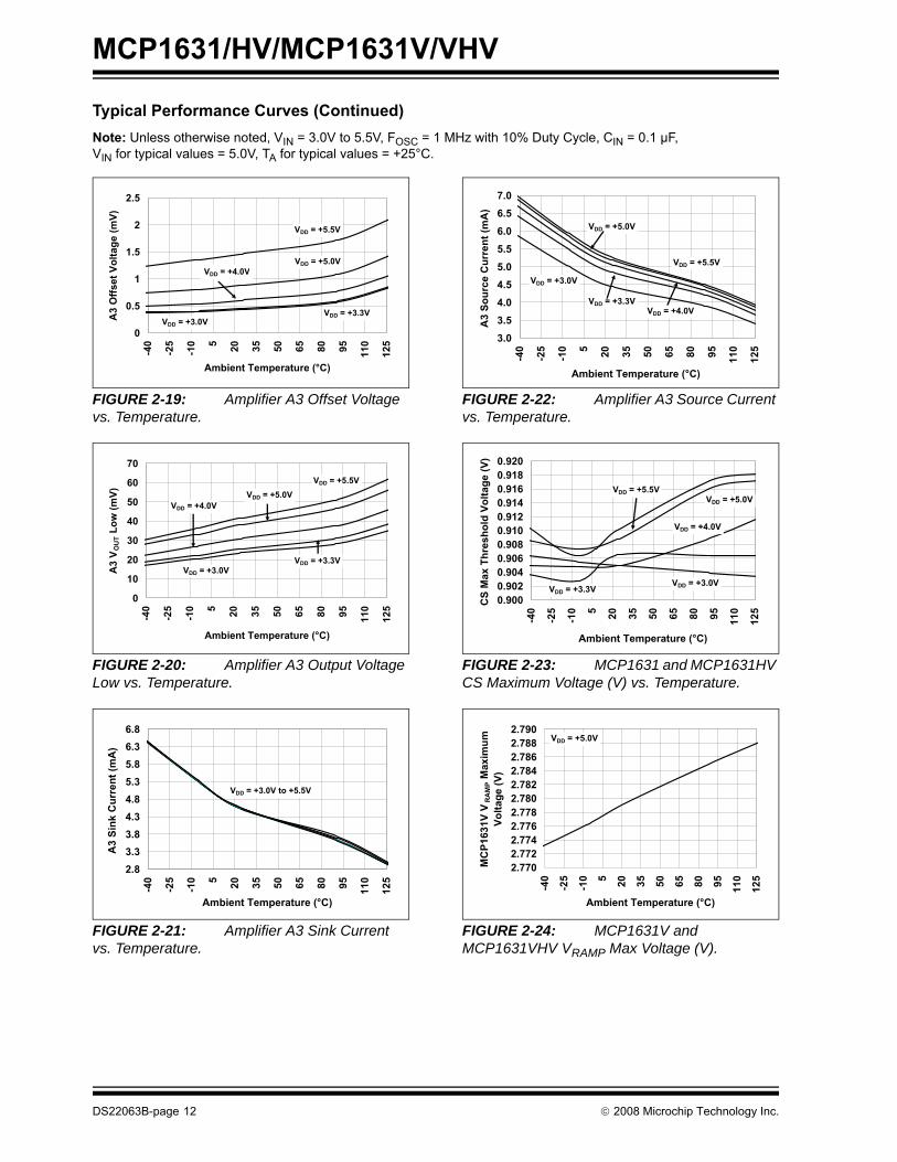
FIGURE 2-19: Amplifier A3 Offset Voltage vs. Temperature.
FIGURE 2-20: Amplifier A3 Output Voltage Low vs. Temperature.
FIGURE 2-21: Amplifier A3 Sink Current vs. Temperature.
FIGURE 2-22: Amplifier A3 Source Current vs. Temperature.
FIGURE 2-23: MCP1631 and MCP1631HV CS Maximum Voltage (V) vs. Temperature.
FIGURE 2-24: MCP1631V and MCP1631VHV VRAMP Max Voltage (V).
0
0.5
1
1.5
2
2.5
-40
-25
-10 5 20 35 50 65 80 95 110
125
Ambient Temperature (°C)
A3
Offs
et V
olta
ge (m
V)
VDD = +3.0VVDD = +3.3V
VDD = +4.0VVDD = +5.0V
VDD = +5.5V
0
10
20
30
40
50
60
70
-40
-25
-10 5 20 35 50 65 80 95 110
125
Ambient Temperature (°C)
A3
VO
UT
Low
(mV)
VDD = +3.0VVDD = +3.3V
VDD = +4.0VVDD = +5.0V
VDD = +5.5V
2.83.33.84.34.85.35.86.36.8
-40
-25
-10 5 20 35 50 65 80 95 110
125
Ambient Temperature (°C)
A3
Sink
Cur
rent
(mA
)
VDD = +3.0V to +5.5V
3.03.54.04.55.05.56.06.57.0
-40
-25
-10 5 20 35 50 65 80 95 110
125
Ambient Temperature (°C)
A3
Sour
ce C
urre
nt (m
A)
VDD = +3.0V
VDD = +3.3VVDD = +4.0V
VDD = +5.0V
VDD = +5.5V
0.9000.9020.9040.9060.9080.9100.9120.9140.9160.9180.920
-40
-25
-10 5 20 35 50 65 80 95 110
125
Ambient Temperature (°C)
CS
Max
Thr
esho
ld V
olta
ge (V
)
VDD = +3.0VVDD = +3.3V
VDD = +4.0V
VDD = +5.0VVDD = +5.5V
2.7702.7722.7742.7762.7782.7802.7822.7842.7862.7882.790
-40
-25
-10 5 20 35 50 65 80 95 110
125
Ambient Temperature (°C)
MC
P163
1V V
RA
MP M
axim
um
Volta
ge (V
)
VDD = +5.0V
DS22063B-page 12 © 2008 Microchip Technology Inc.
MCP1631/HV/MCP1631V/VHV
Typical Performance Curves (Continued)Note: Unless otherwise noted, VIN = 3.0V to 5.5V, FOSC = 1 MHz with 10% Duty Cycle, CIN = 0.1 µF,VIN for typical values = 5.0V, TA for typical values = +25°C.
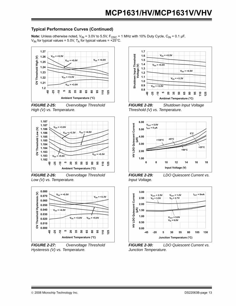
FIGURE 2-25: Overvoltage Threshold High (V) vs. Temperature.
FIGURE 2-26: Overvoltage Threshold Low (V) vs. Temperature.
FIGURE 2-27: Overvoltage Threshold Hysteresis (V) vs. Temperature.
FIGURE 2-28: Shutdown Input Voltage Threshold (V) vs. Temperature.
FIGURE 2-29: LDO Quiescent Current vs. Input Voltage.
FIGURE 2-30: LDO Quiescent Current vs. Junction Temperature.
1.2
1.21
1.22
1.23
1.24
1.25
1.26
1.27-4
0
-25
-10 5 20 35 50 65 80 95 110
125
Ambient Temperature (°C)
OV
Thre
shol
d H
igh
(V)
VDD = +3.0V
VDD = +3.3V
VDD = +4.0VVDD = +5.0V
VDD = +5.5V
1.1821.1831.1831.1841.1841.1851.1851.1861.1861.1871.187
-40
-25
-10 5 20 35 50 65 80 95 110
125
Ambient Temperature (°C)
OV
Thre
shol
d Lo
w (V
) VDD = +3.0V
VDD = +3.3V VDD = +4.0V
VDD = +5.0VVDD = +5.5V
0.0000.0100.0200.0300.0400.0500.0600.0700.080
-40
-25
-10 5 20 35 50 65 80 95 110
125
Ambient Temperature (°C)
OV
Thre
shol
d H
yste
resi
s (V
)
VDD = +3.0V
VDD = +3.3V
VDD = +4.0V
VDD = +5.0V
VDD = +5.5V
0.80.91.01.11.21.31.41.51.61.7
-40
-25
-10 5 20 35 50 65 80 95 110
125
Ambinet Temperature (°C)
Shut
dow
n In
put T
hres
hold
Vo
ltage
(V)
VDD = +3.0V
VDD = +3.3V
VDD = +4.0V
VDD = +5.0V
VDD = +5.5V
1.00
2.00
3.00
4.00
5.00
6.00
6 8 10 12 14 16 18
Input Voltage (V)
HV
LDO
Qui
esce
nt C
urre
nt
(µA
)
VOUT = 5.0VIOUT = 0 µA
+25°C
+130°C -45°C
0°C
+90°C
0.00
0.50
1.00
1.50
2.00
2.50
3.00
-45 -20 5 30 55 80 105 130
Junction Temperature (°C)
HV
LDO
Qui
esce
nt C
urre
nt
(µA
)
IOUT = 0mA
VOUT = 5.0VVIN = 6.0V
VOUT = 1.2VVIN = 2.7V
VOUT = 2.5VVIN = 3.5V
© 2008 Microchip Technology Inc. DS22063B-page 13
MCP1631/HV/MCP1631V/VHV
Typical Performance Curves (Continued)Note: Unless otherwise noted, VIN = 3.0V to 5.5V, FOSC = 1 MHz with 10% Duty Cycle, CIN = 0.1 µF,VIN for typical values = 5.0V, TA for typical values = +25°C.
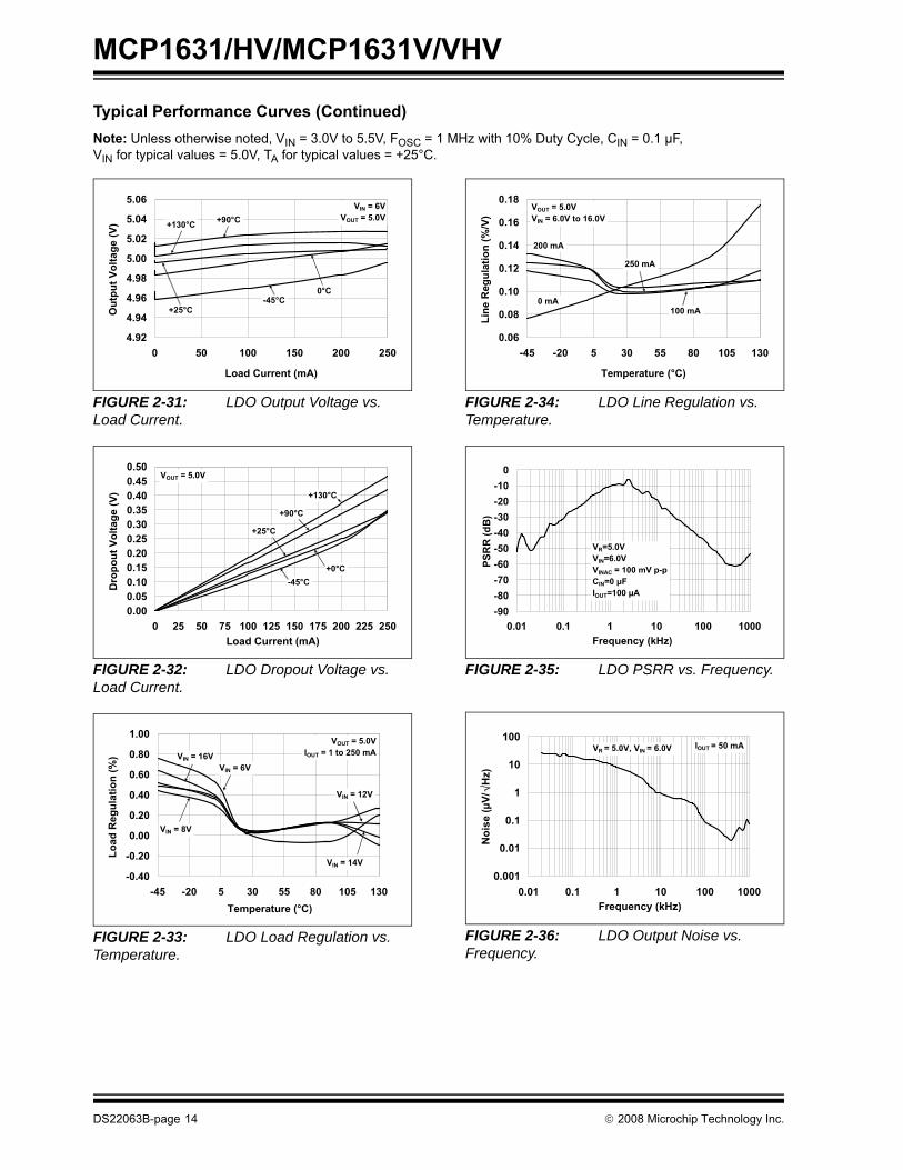
FIGURE 2-31: LDO Output Voltage vs. Load Current.
FIGURE 2-32: LDO Dropout Voltage vs. Load Current.
FIGURE 2-33: LDO Load Regulation vs. Temperature.
FIGURE 2-34: LDO Line Regulation vs. Temperature.
FIGURE 2-35: LDO PSRR vs. Frequency.
FIGURE 2-36: LDO Output Noise vs. Frequency.
4.92
4.94
4.96
4.98
5.00
5.02
5.04
5.06
0 50 100 150 200 250
Load Current (mA)
Out
put V
olta
ge (V
)
VIN = 6VVOUT = 5.0V
+25°C
+130°C
-45°C0°C
+90°C
0.000.050.100.150.200.250.300.350.400.450.50
0 25 50 75 100 125 150 175 200 225 250Load Current (mA)
Dro
pout
Vol
tage
(V)
VOUT = 5.0V
+25°C
+130°C
+0°C-45°C
+90°C
-0.40
-0.20
0.00
0.20
0.40
0.60
0.80
1.00
-45 -20 5 30 55 80 105 130Temperature (°C)
Load
Reg
ulat
ion
(%)
VOUT = 5.0VIOUT = 1 to 250 mA
VIN = 6V
VIN = 14V
VIN = 12V
VIN = 8V
VIN = 16V
0.06
0.08
0.10
0.12
0.14
0.16
0.18
-45 -20 5 30 55 80 105 130
Temperature (°C)
Line
Reg
ulat
ion
(%/V
)
VOUT = 5.0VVIN = 6.0V to 16.0V
200 mA
100 mA0 mA
250 mA
-90-80-70-60-50-40-30-20-10
0
0.01 0.1 1 10 100 1000Frequency (kHz)
PSR
R (d
B)
VR=5.0VVIN=6.0VVINAC = 100 mV p-pCIN=0 μFIOUT=100 µA
0.001
0.01
0.1
1
10
100
0.01 0.1 1 10 100 1000Frequency (kHz)
Noi
se (µ
V/√H
z)
VR = 5.0V, VIN = 6.0V IOUT = 50 mA
DS22063B-page 14 © 2008 Microchip Technology Inc.
MCP1631/HV/MCP1631V/VHV
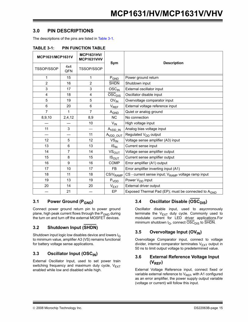
3.0 PIN DESCRIPTIONSThe descriptions of the pins are listed in Table 3-1.
TABLE 3-1: PIN FUNCTION TABLE
3.1 Power Ground (PGND)Connect power ground return pin to power groundplane, high peak current flows through the PGND duringthe turn on and turn off the external MOSFET devices.
3.2 Shutdown Input (SHDN)Shutdown input logic low disables device and lowers IQto minimum value, amplifier A3 (VS) remains functionalfor battery voltage sense applications.
3.3 Oscillator Input (OSCIN)External Oscillator Input, used to set power trainswitching frequency and maximum duty cycle, VEXTenabled while low and disabled while high.
3.4 Oscillator Disable (OSCDIS)Oscillator disable input, used to asycnronouslyterminate the VEXT duty cycle. Commonly used tomodulate current for LED driver applications.Forminimum shutdown IQ, connect OSCDIS to SHDN.
3.5 Overvoltage Input (OVIN)Overvoltage Comparator input, connect to voltagedivider, internal comparator terminates VEXT output in50 ns to limit output voltage to predetermined value.
3.6 External Reference Voltage Input (VREF)
External Voltage Reference input, connect fixed orvariable external reference to VREF, with A1 configuredas an error amplifier, the power supply output variable(voltage or current) will follow this input.
MCP1631/MCP1631V MCP1631HV/MCP1631VHV
Sym DescriptionTSSOP/SSOP 4x4
QFN TSSOP/SSOP
1 15 1 PGND Power ground return2 16 2 SHDN Shutdown input3 17 3 OSCIN External oscillator input4 18 4 OSCDIS Oscillator disable input5 19 5 OVIN Overvoltage comparator input6 20 6 VREF External voltage reference input7 1 7 AGND Quiet or analog ground
8,9,10 2,4,12 8,9 NC No connection— — 10 VIN High voltage input11 3 — AVDD_IN Analog bias voltage input— — 11 AVDD_OUT Regulated VDD output12 5 12 VSIN Voltage sense amplifier (A3) input13 6 13 ISIN Current sense input14 7 14 VSOUT Voltage sense amplifier output15 8 15 ISOUT Current sense amplifier output16 9 16 COMP Error amplifier (A1) output17 10 17 FB Error amplifier inverting input (A1)18 11 18 CS/VRAMP CS - current sense input; VRAMP voltage ramp input19 13 19 PVDD Power VDD input20 14 20 VEXT External driver output— 21 — EP Exposed Thermal Pad (EP); must be connected to AGND
© 2008 Microchip Technology Inc. DS22063B-page 15
MCP1631/HV/MCP1631V/VHV
3.7 Analog Ground (AGND)Quiet or analog ground, connect to analog groundplane to minimize noise on sensitive MCP1631circuitry.
3.8 No Connection (NC)No connection.
3.9 Input Voltage (VIN)High voltage input for MCP1631HV/MCP1631VHVdevices, operates from 3.5V to 16V input supply.
3.10 Analog supply Input (AVDD_IN)Analog bias input, minimum 3.0V to 5.5V operation forMCP1631/MCP1631V devices.
3.11 Analog Supply Output (AVDD_OUT)Regulated VDD output used to power internalM C P 1 6 3 1 H V / M C P 1 6 3 1 V H V a n d e x t e r n a lmicrocontroller, supplies up to 250 ma of bias current at3.3V or 5.0V regulated low drop out rail.
3.12 Voltage Sense Input (VSIN)Voltage sense amplifier (A3) input, connect to highimpedance battery voltage resistor divider to sensebattery voltage with minimal loading.
3.13 Current Sense Input (ISIN)Connect to SEPIC secondary side sense resistor todevelop a regulated current source used to chargemulti-chemistry batteries.
3.14 Voltage Sense Output (VSOUT)Voltage sense amplifier output, connect tomicrocontroller analog to digital converter to measurebattery voltage.
3.15 Current Sense Output (ISOUT)Current sense amplifier output, connect to erroramplifier (A1) inverting input (FB) to regulate SEPICoutput current.
3.16 Error Amplifier Output (COMP)Error amplifier (A1) output, connect control loopcompensation from FB input to COMP output pin.
3.17 Feedback (FB)Error amplifier input (A1), connect to current senseoutput amplifier (A2) to regulate current.
3.18 Current Sense or Voltage Ramp (CS/VRAMP)
For MCP1631/MCP1631HV applications, connect tolow side current sense of SEPIC switch for currentmode control and peak current limit. For MCP1631/MCP1631HV application, connect artificial rampvoltage to VRAMP input for voltage mode PWM control.
3.19 Power VDD (PVDD)Power VDD input, VEXT gate drive supply input, connectto +5.0V or +3.3V supply for driving external MOSFET.
3.20 External Driver (VEXT)High current driver output used to drive externalMOSFET at high frequency, capable of 1A peakcurrents with +5.0V PVDD.
3.21 Exposed PAD 4x4 QFN (EP)There is an internal electrical connection between theExposed Thermal Pad (EP) and the AGND pin; theymust be connected to the same potential on the PrintedCircuit Board (PCB).
DS22063B-page 16 © 2008 Microchip Technology Inc.
MCP1631/HV/MCP1631V/VHV
4.0 DETAILED DESCRIPTION
4.1 Device OverviewThe MCP1631/MCP1631V device family combines theanalog functions to develop high frequency switchmode power systems while integrating features forbattery charger and LED current source applications.With the integration of a MOSFET driver, voltagesense, current sense and over voltage protection, theMCP1631/MCP1631V is a highly integrated, high-speed analog pulse width modulator.
The MCP1631/MCP1631V output (VEXT) is used tocontrol the switch of the power system (on and offtime). By controlling the switch on and off time, thepower system output can be regulated. With theoscillator and reference voltage as inputs, a simpleinterface to a microcontroller is available with theMCP1631/MCP1631V to develop intelligent powersystems. A good example of an intelligent powersystem is a battery charger, programmable LED drivercurrent source or programmable power supply.
The MCP1631/MCP1631V is a combination ofspecialty analog blocks consisting of a Pulse WidthModulator (PWM), MOSFET Driver, Current SenseAmplifier (A2), Voltage Sense Amplifier (A3),Overvoltage Comparator (C2) and additional features(Shutdown, Undervoltage Lockout, OvertemperatureProtection). For the HV options, an internal low dropoutregulator is integrated for operation from high voltageinputs (MCP1631HV/MCP1631VHV).
4.2 Pulse Width Modulator (PWM)The internal PWM of the MCP1631/MCP1631V iscomprised of an error amplifier, high-speed comparatorand latch. The output of the amplifier is compared toeither the MCP1631 CS (primary current sense input)or the MCP1631V VRAMP (voltage mode ramp input) ofthe high speed comparator. When the CS or VRAMPsignal reach the level of the error amplifier output, theon cycle is terminated and the external switch islatched off until the beginning of the next cycle (high tolow transition of OSCIN).
4.3 VEXT MOSFET DriverThe MCP1631/MCP1631V output can be used to drivethe external MOSFET directly for low side topologyapplications. The VEXT is capable of sourcing up to700 mA and sinking up to 1A of current from a PVDDsource of 5V. Typical output power using the VEXToutput to directly drive the external MOSFET canexceed 50W depending upon application and switchingfrequency.
4.4 Current Sense Amplifier (A2)The A2 current sense amplifier is used to sense currentin the secondary side of a SEPIC converter orfreewheeling current in a Buck converter. The invertingamplifier has a built in voltage gain of ten with low offsetand high speed.
4.5 Voltage Sense Amplifier (A3)The A3 voltage sense amplifier is used to sense batteryvoltage. In battery powered applications, it is importantto minimize the steady stage load current draw on thebattery. The voltage sense amplifier (A3) is used tobuffer a high impedance series divider used to reducethe battery pack voltage to a level that can be readusing an analog to digital converter. The voltage senseamplifier draws a very low quiescent current andremains functional when the MCP1631/MCP1631V isshutdown making it possible to read battery voltagewithout turning on the charger.
4.6 Overvoltage Comparator(C2)The C2 overvoltage comparator is used to prevent thepower system from being damaged when the load(battery) is disconnected. By comparing the divideddown power train output voltage with a 1.2V internalreference voltage, the MCP1631/MCP1631V VEXToutput switching is interrupted when the output voltageis above a pre-set value. This limits the output voltageof the power train, the 0V comparator’s hysteresis willoperate as a ripple regulator.
4.7 Shutdown InputThe MCP1631/MCP1631V shutdown feature is used todisable the device with the exception of the voltagesense amplifier A3 to minimize quiescent current draw.While shutdown, A3 remains operational while thedevice draws 4.4 µA from the input.
4.8 ProtectionThe MCP1631/MCP1631V has built in UndervoltageLockout (UVLO) that ensures the output VEXT pin isforced to a known state (low) when the input voltage orAVDD is below the specified value. This prevents themain MOSFET switch from being turned on during apower up or down sequence.
The MCP1631/MCP1631V provides a thermalshutdown protection feature, if the internal junctiontemperature of the device becomes high, theovertemperature protection feature will disable (pull theVEXT output low) and shut down the power train.
© 2008 Microchip Technology Inc. DS22063B-page 17
MCP1631/HV/MCP1631V/VHV
NOTES:
DS22063B-page 18 © 2008 Microchip Technology Inc.
MCP1631/HV/MCP1631V/VHV
5.0 APPLICATION INFORMATION
5.1 Typical ApplicationsThe MCP1631/MCP1631V can be used to developintelligent power management solutions, typicalapplications include a multi-chemistry battery chargerused to charge Li-Ion, NiMH or NiCd batteries andconstant current LED drivers.
5.2 Battery Charger Design OverviewThe design approach for developing high currentswitching battery chargers using the MCP1631 isdescribed in this section. Depending on input voltagerange, there are two versions of the device that can beused to accommodate a very wide range of inputvoltages.
For a regulated input voltage range of 5V, theMCP1631/MCP1631V device is used, for this inputvoltage application (regulated ac-dc converter or USBinput), the MCP1631/MCP1631V is powered directlyfrom the 5V dc input.
For input voltages to +16V steady state with +18Vtransients, the MCP1631HV/MCP1631VHV, or highvoltage option can be used. The high voltage devicesintegrate a low dropout (LDO) linear regulator with a setoutput voltage of +3.3V or +5.0V that internally powersthe MCP1631HV/MCP1631VHV and is also capable ofproviding 250 mA of bias current for the attachedmicrocontroller and other circuitry. MCP1631HV/MCP1631VHV internal power dissipation must beconsidered when loading the internal LDO regulator.
For higher input voltages the MCP1631/MCP1631Vcan be biased from an external regulated +3.0V to+5.5V supply.
5.3 Programmable Single Ended Primary Inductive (SEPIC) Current Source
The MCP1631/MCP1631V family integrates featuresthat are necessary to develop programmable currentsources. The SEPIC converter is commonly used inbattery charger applications. The primary or inputinductor is used to filter input current and minimize theswitching noise at the converter input. The primary tosecondary capacitive isolation blocks any dc path frominput to output making the SEPIC safer than Buck orother non-isolated topologies. The SEPIC rectifierblocks the reverse path preventing battery leakage, inother topologies an additional diode for blocking isnecessary adding additional components andefficiency loss.
The input or primary inductor and output or secondaryinductor are typically constructed from a singlemagnetic device with two windings, this is commonlyreferred to as a coupled inductor. Using coupled
inductors has significant advantages in addition to thesize and cost benefits of a single core with multiplewindings.
5.4 Mixed Signal DesignFor intelligent battery charger design, a microcontrolleris used to generate the proper charge profile, chargetermination, safety timers and battery charger features.When using the MCP1631/MCP1631V for Li-Ionbattery charger applications, the microcontroller is alsoused to generate the constant voltage regulation phaseof the charge cycle. This is accomplished by using theexternal reference feature of the MCP1631/MCP1631Vas a programmable current source. The microcontrolleris used to vary the VREF input of the MCP1631/MCP1631V. The charge current into the battery isregulated by the MCP1631/MCP1631V, the level that itis regulated to is set by the programmability of themicrocontroller.
The internal MCP1631/MCP1631V analog compo-nents are used to regulate the microcontrollerprogrammed current. The secondary or battery currentis sensed using amplifier A2, the output of A2 is feedinto the input of the error amplifier A1, the output of A1sets the peak switch current of the SEPIC converter, itincreases or decreases the battery current to match its(A1) inputs. By increasing the VREF or non-invertinginput of A1, the battery current is increased.
5.5 Safety FeaturesThe MCP1631/MCP1631V integrates a high-speedcomparator used to protect the charger and batteryfrom being exposed to high voltages if the battery isremoved or opens. Comparator C2 is used to sense theSEPIC output voltage. If the divided down outputvoltage becomes higher than the 1.2V internalMCP1631/MCP1631V reference, the VEXT PWMoutput is terminated within 50 ns preventing the buildup of voltage on the SEPIC output.
Peak switch current is limited by the MCP1631/MCP1631V comparator C1 and error amplifier A1output voltage clamp. For the MCP1631, the erroramplifier output is clamped at 2.7V. The A1 output isdivided down by 1/3 and compared with CS (currentsense) input. The VEXT output is turned off if the CSinput reaches a level of 1/3 of 2.7V or 0.9V in 12 ns,preventing the external switch current from becominghigh enough to damage the SEPIC power train.
Internal overtemperature protection limits the devicejunction temperature to 150°C preventing catastrophicfailure for overtemperature conditions. Once thetemperature decreases 10°C, the device will resumenormal operation.
Safety timers are typically used to limit the amount ofenergy into a faulted battery or pack. This isaccomplished using the microcontroller and MCP1631/MCP1631V shutdown feature.
© 2008 Microchip Technology Inc. DS22063B-page 19
MCP1631/HV/MCP1631V/VHV
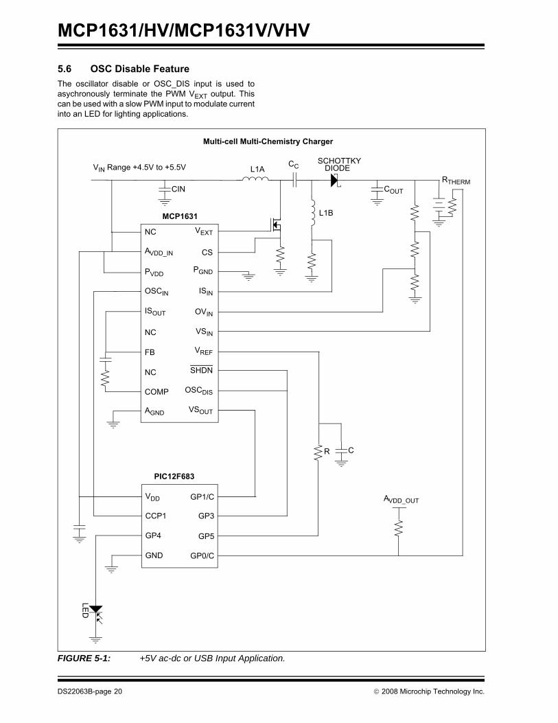
5.6 OSC Disable FeatureThe oscillator disable or OSC_DIS input is used toasychronously terminate the PWM VEXT output. Thiscan be used with a slow PWM input to modulate currentinto an LED for lighting applications.
FIGURE 5-1: +5V ac-dc or USB Input Application.
COMP
PGND
SHDN
OSCIN
OSCDIS
OVIN
VREF
AGND
NC
NC
AVDD_IN
VSIN
ISIN
VSOUT
ISOUT
FB
CS
PVDD
VEXT
L1A
CIN
SCHOTTKYDIODE
COUT
L1B
CC
MCP1631
AVDD_OUT
GP0/C
C
GP5
GP3
GP1/C
PIC12F683LE
D
R
GND
GP4
CCP1
VDD
VIN Range +4.5V to +5.5V
Multi-cell Multi-Chemistry Charger
NC
RTHERM
DS22063B-page 20 © 2008 Microchip Technology Inc.
MCP1631/HV/MCP1631V/VHV
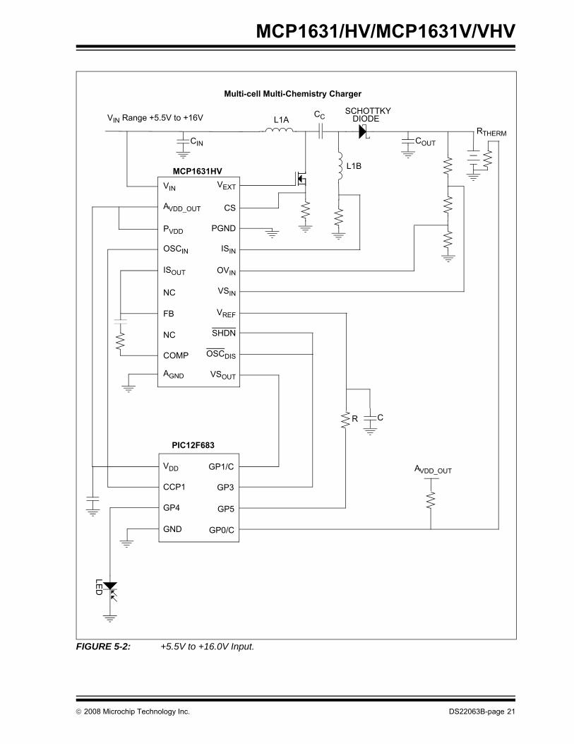
FIGURE 5-2: +5.5V to +16.0V Input.
COMP
PGND
SHDN
OSCIN
OSCDIS
OVIN
VREF
AGND
NC
NC
AVDD_OUT
VSIN
ISIN
VSOUT
ISOUT
FB
CS
PVDD
VEXT
L1A
CIN
SCHOTTKYDIODE
COUT
L1B
CC
MCP1631HVVIN
AVDD_OUT
C
PIC12F683
LED
R
VIN Range +5.5V to +16V
Multi-cell Multi-Chemistry Charger
GP0/C
GP5
GP3
GP1/C
GND
GP4
CCP1
VDD
RTHERM
© 2008 Microchip Technology Inc. DS22063B-page 21
MCP1631/HV/MCP1631V/VHV
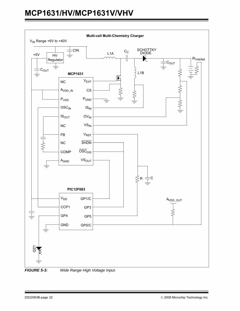
FIGURE 5-3: Wide Range High Voltage Input.
L1ACIN SCHOTTKY
DIODE
COUT
L1B
CC
MCP1631
AVDD_OUT
C
PIC12F683
LED
R
VIN Range +6V to +40VMulti-cell Multi-Chemistry Charger
COUT
+5V HV Regulator
COMP
PGND
SHDN
OSCIN
OSCDIS
OVIN
VREF
AGND
NC
NC
AVDD_IN
VSIN
ISIN
VSOUT
FB
CS
PVDD
VEXTNC
ISOUT
GP0/C
GP5
GP3
GP1/C
GND
GP4
CCP1
VDD
RTHERM
DS22063B-page 22 © 2008 Microchip Technology Inc.
MCP1631/HV/MCP1631V/VHV
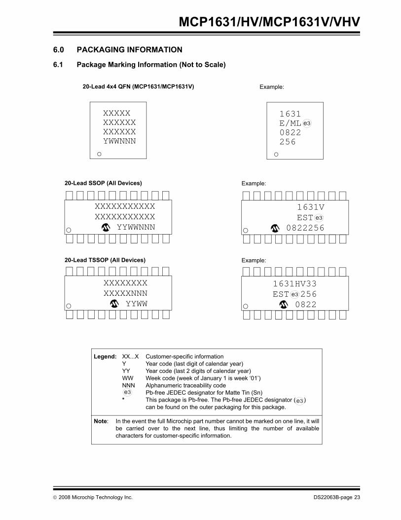
6.0 PACKAGING INFORMATION
6.1 Package Marking Information (Not to Scale)
Legend: XX...X Customer-specific informationY Year code (last digit of calendar year)YY Year code (last 2 digits of calendar year)WW Week code (week of January 1 is week ‘01’)NNN Alphanumeric traceability code Pb-free JEDEC designator for Matte Tin (Sn)* This package is Pb-free. The Pb-free JEDEC designator ( )
can be found on the outer packaging for this package.
Note: In the event the full Microchip part number cannot be marked on one line, it willbe carried over to the next line, thus limiting the number of availablecharacters for customer-specific information.
3e
3e
20-Lead SSOP (All Devices)
20-Lead 4x4 QFN (MCP1631/MCP1631V)
20-Lead TSSOP (All Devices)
XXXXXXXXXXXXXXXXXYWWNNN
XXXXXXXXXXXXXXXXXXXXXX
YYWWNNN
XXXXXXXXXXXXXNNN
YYWW
Example:
Example:
Example:
1631E/ML^^0822256
1631VEST^^
0822256
1631HV33EST^^256
08223e
3e
3e
© 2008 Microchip Technology Inc. DS22063B-page 23
MCP1631/HV/MCP1631V/VHV
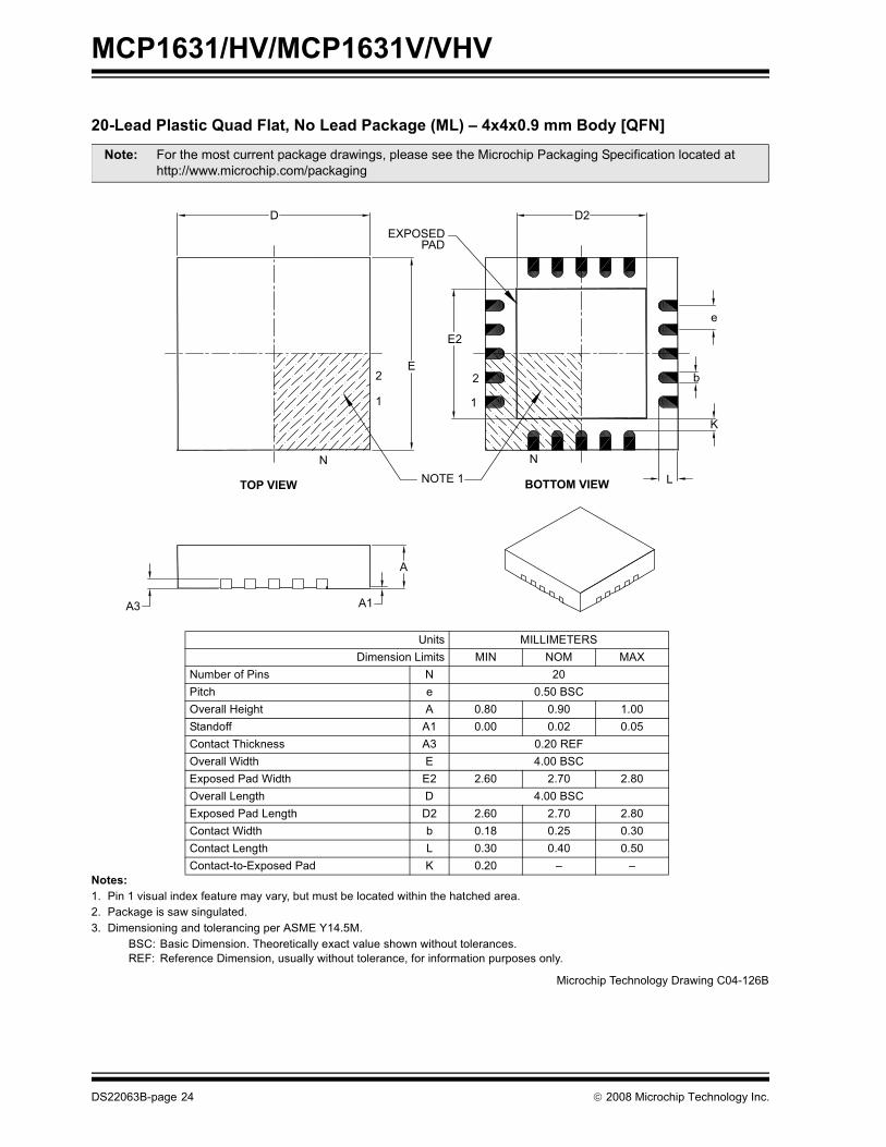
!"#$
% !"#$%!&'(!%&! %(%")%%%" * ) !%"+ & "%,-.
/01 / & %#%! ))%!%% ,21 $& '! !)%!%%'$$&%!
% 2%& %!%*") ' %*$%%"%%%133)))&&3*
4% 55, ,& 5&% 6 67 8
6!&($ 6 % ./079% : %"$$ .0%% * + ,27;"% , /0,# "";"% , < :75% /0,# ""5% < :0%%;"% ( : . +0%%5% 5 + .0%%%,# "" = > >
DEXPOSED
PAD
E
E2
2
1
N
TOP VIEW NOTE 1
N
L
K
b
e
D2
2
1
A
A1A3
BOTTOM VIEW
) 0</
DS22063B-page 24 © 2008 Microchip Technology Inc.
MCP1631/HV/MCP1631V/VHV
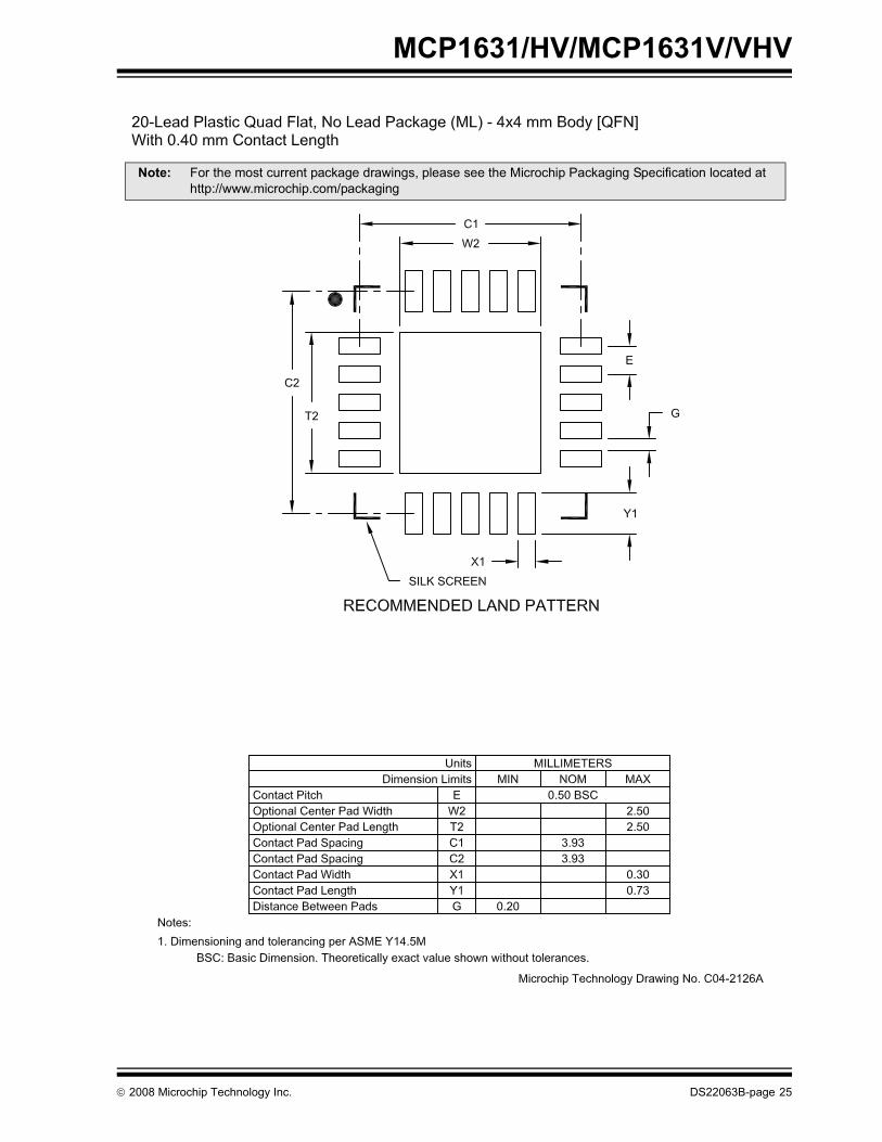
% 2%& %!%*") ' %*$%%"%%%133)))&&3*
© 2008 Microchip Technology Inc. DS22063B-page 25
MCP1631/HV/MCP1631V/VHV
&'()& * )&&+, !"#&&*$
% !"#$%!&'(!%&! %(%")%%%" & ","%!"&"$ %! "$ %! %#"&& "+ & "%,-.
/01 / & %#%! ))%!%% ,21 $& '! !)%!%%'$$&%!
% 2%& %!%*") ' %*$%%"%%%133)))&&3*
4% 55, ,& 5&% 6 67 8
6!&($ 6 % <./079% > > ""* * <. . :.%"$$ . > >7;"% , : :""*;"% , . .+ .<75% < .2%5% 5 .. . .2%% 5 .,25" * > .2% ? ? :?5";"% ( > +:
φ
LL1
A2c
eb
A1
A
1 2
NOTE 1
E1
E
D
N
) 0/
DS22063B-page 26 © 2008 Microchip Technology Inc.
MCP1631/HV/MCP1631V/VHV
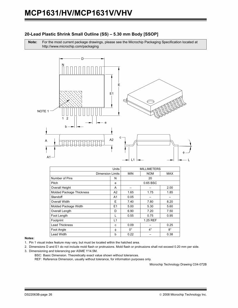
-')&'()& * )&- !"#-&&*$
% !"#$%!&'(!%&! %(%")%%%" & ","%!"&"$ %! "$ %! %#".&& "+ & "%,-.
/01 / & %#%! ))%!%% ,21 $& '! !)%!%%'$$&%!
% 2%& %!%*") ' %*$%%"%%%133)))&&3*
4% 55, ,& 5&% 6 67 8
6!&($ 6 % <./079% > > ""* * : .%"$$ . > .7;"% , </0""*;"% , + .""*5% < <. <<2%5% 5 . < .2%% 5 ,22% ? > :?5" * > 5";"% ( > +
D
E
E1
NOTE 1
1 2
b e
A
A1
A2c
L1 L
φ
N
) 0::/
© 2008 Microchip Technology Inc. DS22063B-page 27
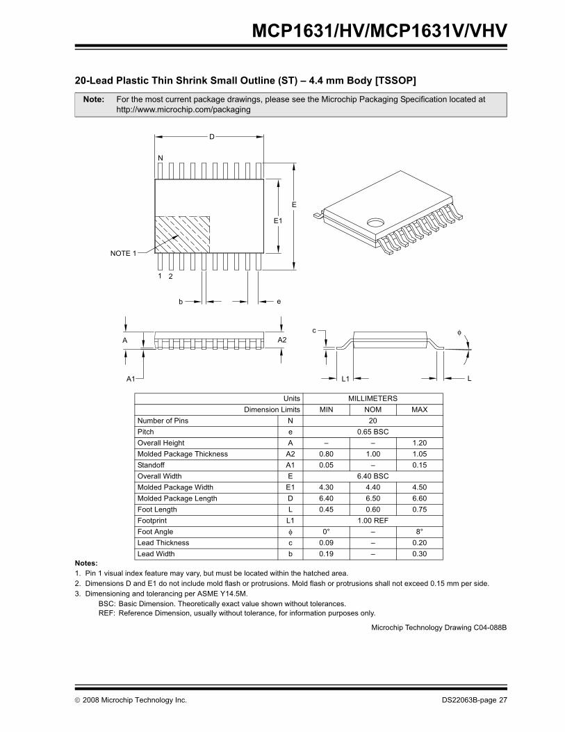
MCP1631/HV/MCP1631V/VHV
NOTES:
DS22063B-page 28 © 2008 Microchip Technology Inc.
MCP1631/HV/MCP1631V/VHV
APPENDIX A: REVISION HISTORY
Revision B (October 2008)The following is the list of modifications:
1. Section 2.0 “Typical Performance Curves”,Input Offset Voltage: changed minimum, typical,maximum from -0.6, -, +0.6 to -5, -0.6, +5,respectively;
2. Updated Section 6.0 “Packaging Informa-tion”;
3. Updated the Product Identification System.
Revision A (October 2007)• Original Release of this Document.
© 2008 Microchip Technology Inc. DS22063B-page 29

MCP1631/HV/MCP1631V/VHV
NOTES:DS22063B-page 30 © 2008 Microchip Technology Inc.
MCP1631/HV/MCP1631V/VHV
PRODUCT IDENTIFICATION SYSTEMTo order or obtain information, e.g., on pricing or delivery, refer to the factory or the listed sales office.
PART NO. X /XX
PackageTemperatureRange
Device
Device MCP1631: High-Speed PWM
MCP1631T: High-Speed PWMTape and Reel
MCP1631HV: High-Speed PWMMCP1631HVT: High-Speed PWM
Tape and ReelMCP1631HV: High-Speed PWMMCP1631HVT: High-Speed PWM
Tape and ReelMCP1631VHV: High-Speed PWMMCP1631VHVT: High-Speed PWM
Tape and Reel
Voltage options 330 = 3.3V500 = 5.0V
Temperature Range E = -40°C to +125°C
Package ML = Plastic Quad Flat, No Lead (4x4x0.9), 20-leadSS = Plastic Shrink Small Outline (5.30 mm), 20-leadST = Plastic Thin Shrink Small Outline (4.4 mm),
20-Lead
* All package offerings are Pb Free (Lead Free)
Examples:a) MCP1631-E/ML: High-Speed PWM,
20LD QFN package.b) MCP1631-E/SS: High-Speed PWM,
20LD SSOP package.c) MCP1631-E/ST: High-Speed PWM,
20LD TSSOP package.
a) MCP1631HV-330E/SS:High Speed PWM,Current Mode Control, 3.3V Internal Regulator, 20LD SSOP Package.
b) MCP1631HV-500E/SS: High Speed PWM, Current Mode Control, 5.0V Internal Regulator, 20LD SSOP Package.
c) MCP1631HV-500E/ST:High Speed PWM, Current Mode Control, 5.0V Internal Regulator, 20LD TSSOP Package.
a) MCP1631VHVT-500E/ST:High Speed PWM, Voltage Mode Control, 5.0V Internal Regulator, 20LD TSSOP Package.
b) MCP1631VHV-330E/SS: High Speed PWM, Voltage Mode Control, 3.3V Internal Regulator, 20LD SSOP Package.
c) MCP1631VHV-330E/ST:High Speed PWM, Voltage Mode Control, 3.3V Internal Regulator, 20LD TSSOP Package.
-XXX
VoltageOptions
© 2008 Microchip Technology Inc. DS22063B-page 31
MCP1631/HV/MCP1631V/VHV
NOTES:DS22063B-page 32 © 2008 Microchip Technology Inc.
Note the following details of the code protection feature on Microchip devices:• Microchip products meet the specification contained in their particular Microchip Data Sheet.
• Microchip believes that its family of products is one of the most secure families of its kind on the market today, when used in the intended manner and under normal conditions.
• There are dishonest and possibly illegal methods used to breach the code protection feature. All of these methods, to our knowledge, require using the Microchip products in a manner outside the operating specifications contained in Microchip’s Data Sheets. Most likely, the person doing so is engaged in theft of intellectual property.
• Microchip is willing to work with the customer who is concerned about the integrity of their code.
• Neither Microchip nor any other semiconductor manufacturer can guarantee the security of their code. Code protection does not mean that we are guaranteeing the product as “unbreakable.”
Code protection is constantly evolving. We at Microchip are committed to continuously improving the code protection features of ourproducts. Attempts to break Microchip’s code protection feature may be a violation of the Digital Millennium Copyright Act. If such actsallow unauthorized access to your software or other copyrighted work, you may have a right to sue for relief under that Act.
Information contained in this publication regarding deviceapplications and the like is provided only for your convenienceand may be superseded by updates. It is your responsibility toensure that your application meets with your specifications.MICROCHIP MAKES NO REPRESENTATIONS ORWARRANTIES OF ANY KIND WHETHER EXPRESS ORIMPLIED, WRITTEN OR ORAL, STATUTORY OROTHERWISE, RELATED TO THE INFORMATION,INCLUDING BUT NOT LIMITED TO ITS CONDITION,QUALITY, PERFORMANCE, MERCHANTABILITY ORFITNESS FOR PURPOSE. Microchip disclaims all liabilityarising from this information and its use. Use of Microchipdevices in life support and/or safety applications is entirely atthe buyer’s risk, and the buyer agrees to defend, indemnify andhold harmless Microchip from any and all damages, claims,suits, or expenses resulting from such use. No licenses areconveyed, implicitly or otherwise, under any Microchipintellectual property rights.
© 2008 Microchip Technology Inc.
Trademarks
The Microchip name and logo, the Microchip logo, Accuron, dsPIC, KEELOQ, KEELOQ logo, MPLAB, PIC, PICmicro, PICSTART, rfPIC, SmartShunt and UNI/O are registered trademarks of Microchip Technology Incorporated in the U.S.A. and other countries.
FilterLab, Linear Active Thermistor, MXDEV, MXLAB, SEEVAL, SmartSensor and The Embedded Control Solutions Company are registered trademarks of Microchip Technology Incorporated in the U.S.A.
Analog-for-the-Digital Age, Application Maestro, CodeGuard, dsPICDEM, dsPICDEM.net, dsPICworks, dsSPEAK, ECAN, ECONOMONITOR, FanSense, In-Circuit Serial Programming, ICSP, ICEPIC, Mindi, MiWi, MPASM, MPLAB Certified logo, MPLIB, MPLINK, mTouch, PICkit, PICDEM, PICDEM.net, PICtail, PIC32 logo, PowerCal, PowerInfo, PowerMate, PowerTool, REAL ICE, rfLAB, Select Mode, Total Endurance, WiperLock and ZENA are trademarks of Microchip Technology Incorporated in the U.S.A. and other countries.
SQTP is a service mark of Microchip Technology Incorporated in the U.S.A.
All other trademarks mentioned herein are property of their respective companies.
© 2008, Microchip Technology Incorporated, Printed in the U.S.A., All Rights Reserved.
Printed on recycled paper.
DS22063B-page 33
Microchip received ISO/TS-16949:2002 certification for its worldwide headquarters, design and wafer fabrication facilities in Chandler and Tempe, Arizona; Gresham, Oregon and design centers in California and India. The Company’s quality system processes and procedures are for its PIC® MCUs and dsPIC® DSCs, KEELOQ® code hopping devices, Serial EEPROMs, microperipherals, nonvolatile memory and analog products. In addition, Microchip’s quality system for the design and manufacture of development systems is ISO 9001:2000 certified.
DS22063B-page 34 © 2008 Microchip Technology Inc.
AMERICASCorporate Office2355 West Chandler Blvd.Chandler, AZ 85224-6199Tel: 480-792-7200 Fax: 480-792-7277Technical Support: http://support.microchip.comWeb Address: www.microchip.comAtlantaDuluth, GA Tel: 678-957-9614 Fax: 678-957-1455BostonWestborough, MA Tel: 774-760-0087 Fax: 774-760-0088ChicagoItasca, IL Tel: 630-285-0071 Fax: 630-285-0075DallasAddison, TX Tel: 972-818-7423 Fax: 972-818-2924DetroitFarmington Hills, MI Tel: 248-538-2250Fax: 248-538-2260KokomoKokomo, IN Tel: 765-864-8360Fax: 765-864-8387Los AngelesMission Viejo, CA Tel: 949-462-9523 Fax: 949-462-9608Santa ClaraSanta Clara, CA Tel: 408-961-6444Fax: 408-961-6445TorontoMississauga, Ontario, CanadaTel: 905-673-0699 Fax: 905-673-6509
ASIA/PACIFICAsia Pacific OfficeSuites 3707-14, 37th FloorTower 6, The GatewayHarbour City, KowloonHong KongTel: 852-2401-1200Fax: 852-2401-3431Australia - SydneyTel: 61-2-9868-6733Fax: 61-2-9868-6755China - BeijingTel: 86-10-8528-2100 Fax: 86-10-8528-2104China - ChengduTel: 86-28-8665-5511Fax: 86-28-8665-7889China - Hong Kong SARTel: 852-2401-1200 Fax: 852-2401-3431China - NanjingTel: 86-25-8473-2460Fax: 86-25-8473-2470China - QingdaoTel: 86-532-8502-7355Fax: 86-532-8502-7205China - ShanghaiTel: 86-21-5407-5533 Fax: 86-21-5407-5066China - ShenyangTel: 86-24-2334-2829Fax: 86-24-2334-2393China - ShenzhenTel: 86-755-8203-2660 Fax: 86-755-8203-1760China - WuhanTel: 86-27-5980-5300Fax: 86-27-5980-5118China - XiamenTel: 86-592-2388138 Fax: 86-592-2388130China - XianTel: 86-29-8833-7252Fax: 86-29-8833-7256China - ZhuhaiTel: 86-756-3210040 Fax: 86-756-3210049
ASIA/PACIFICIndia - BangaloreTel: 91-80-4182-8400 Fax: 91-80-4182-8422India - New DelhiTel: 91-11-4160-8631Fax: 91-11-4160-8632India - PuneTel: 91-20-2566-1512Fax: 91-20-2566-1513Japan - YokohamaTel: 81-45-471- 6166 Fax: 81-45-471-6122Korea - DaeguTel: 82-53-744-4301Fax: 82-53-744-4302Korea - SeoulTel: 82-2-554-7200Fax: 82-2-558-5932 or 82-2-558-5934Malaysia - Kuala LumpurTel: 60-3-6201-9857Fax: 60-3-6201-9859Malaysia - PenangTel: 60-4-227-8870Fax: 60-4-227-4068Philippines - ManilaTel: 63-2-634-9065Fax: 63-2-634-9069SingaporeTel: 65-6334-8870Fax: 65-6334-8850Taiwan - Hsin ChuTel: 886-3-572-9526Fax: 886-3-572-6459Taiwan - KaohsiungTel: 886-7-536-4818Fax: 886-7-536-4803Taiwan - TaipeiTel: 886-2-2500-6610 Fax: 886-2-2508-0102Thailand - BangkokTel: 66-2-694-1351Fax: 66-2-694-1350
EUROPEAustria - WelsTel: 43-7242-2244-39Fax: 43-7242-2244-393Denmark - CopenhagenTel: 45-4450-2828 Fax: 45-4485-2829France - ParisTel: 33-1-69-53-63-20 Fax: 33-1-69-30-90-79Germany - MunichTel: 49-89-627-144-0 Fax: 49-89-627-144-44Italy - Milan Tel: 39-0331-742611 Fax: 39-0331-466781Netherlands - DrunenTel: 31-416-690399 Fax: 31-416-690340Spain - MadridTel: 34-91-708-08-90Fax: 34-91-708-08-91UK - WokinghamTel: 44-118-921-5869Fax: 44-118-921-5820
WORLDWIDE SALES AND SERVICE
01/02/08