Embed Size (px)
Citation preview
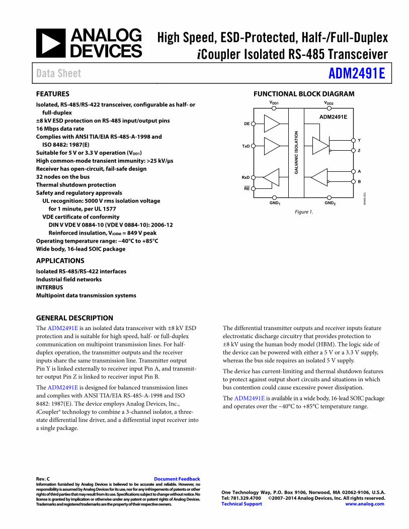
High Speed, ESD-Protected, Half-/Full-Duplex iCoupler Isolated RS-485 Transceiver
Data Sheet ADM2491E
Rev. C Document Feedback Information furnished by Analog Devices is believed to be accurate and reliable. However, no responsibility is assumed by Analog Devices for its use, nor for any infringements of patents or other rights of third parties that may result from its use. Specifications subject to change without notice. No license is granted by implication or otherwise under any patent or patent rights of Analog Devices. Trademarks and registered trademarks are the property of their respective owners.
One Technology Way, P.O. Box 9106, Norwood, MA 02062-9106, U.S.A.Tel: 781.329.4700 ©2007–2014 Analog Devices, Inc. All rights reserved. Technical Support www.analog.com
FEATURES Isolated, RS-485/RS-422 transceiver, configurable as half- or
full-duplex ±8 kV ESD protection on RS-485 input/output pins 16 Mbps data rate Complies with ANSI TIA/EIA RS-485-A-1998 and
ISO 8482: 1987(E) Suitable for 5 V or 3.3 V operation (VDD1) High common-mode transient immunity: >25 kV/μs Receiver has open-circuit, fail-safe design 32 nodes on the bus Thermal shutdown protection Safety and regulatory approvals
UL recognition: 5000 V rms isolation voltage for 1 minute, per UL 1577
VDE certificate of conformity DIN V VDE V 0884-10 (VDE V 0884-10): 2006-12 Reinforced insulation, VIORM = 849 V peak
Operating temperature range: −40°C to +85°C Wide body, 16-lead SOIC package
APPLICATIONS Isolated RS-485/RS-422 interfaces Industrial field networks INTERBUS Multipoint data transmission systems
FUNCTIONAL BLOCK DIAGRAM VDD1
GND1
A
B
VDD2
GND2
Y
ZTxD
DE
RxD
ADM2491E
0698
5-00
1
GA
LVA
NIC
IS
OL
AT
ION
RE
Figure 1.
GENERAL DESCRIPTION The ADM2491E is an isolated data transceiver with ±8 kV ESD protection and is suitable for high speed, half- or full-duplex communication on multipoint transmission lines. For half-duplex operation, the transmitter outputs and the receiver inputs share the same transmission line. Transmitter output Pin Y is linked externally to receiver input Pin A, and transmit-ter output Pin Z is linked to receiver input Pin B.
The ADM2491E is designed for balanced transmission lines and complies with ANSI TIA/EIA RS-485-A-1998 and ISO 8482: 1987(E). The device employs Analog Devices, Inc., iCoupler® technology to combine a 3-channel isolator, a three-state differential line driver, and a differential input receiver into a single package.
The differential transmitter outputs and receiver inputs feature electrostatic discharge circuitry that provides protection to ±8 kV using the human body model (HBM). The logic side of the device can be powered with either a 5 V or a 3.3 V supply, whereas the bus side requires an isolated 5 V supply.
The device has current-limiting and thermal shutdown features to protect against output short circuits and situations in which bus contention could cause excessive power dissipation.
The ADM2491E is available in a wide body, 16-lead SOIC package and operates over the −40°C to +85°C temperature range.
ADM2491E Data Sheet
Rev. C | Page 2 of 16
TABLE OF CONTENTS Features .............................................................................................. 1 Applications ....................................................................................... 1 Functional Block Diagram .............................................................. 1 General Description ......................................................................... 1 Revision History ............................................................................... 2 Specifications ..................................................................................... 3
Timing Specifications .................................................................. 4 Package Characteristics ............................................................... 4 Regulatory Information ............................................................... 4 Insulation and Safety-Related Specifications ............................ 5 VDE 0884 Insulation Characteristics ........................................ 5
Absolute Maximum Ratings ............................................................ 6 ESD Caution .................................................................................. 6
Pin Configuration and Functional Descriptions .......................... 7 Test Circuits ....................................................................................... 8
Switching Characteristics .................................................................9 Typical Performance Characteristics ........................................... 10 Circuit Description......................................................................... 12
Electrical Isolation ...................................................................... 12 Truth Tables................................................................................. 12 Thermal Shutdown .................................................................... 13 Fail-Safe Receiver Inputs ........................................................... 13 Magnetic Field Immunity .......................................................... 13
Applications Information .............................................................. 14 Isolated Power Supply Circuit .................................................. 14 PCB Layout ................................................................................. 14 Typical Applications ................................................................... 15
Outline Dimensions ....................................................................... 16 Ordering Guide .......................................................................... 16
REVISION HISTORY 5/14—Rev. B to Rev. C
Changed VIORM from 848 V peak to 849 V peak (Throughout) . 1 Changes to VDE 0884 Insulation Characteristics Conditions ... 5 Changes to Ordering Guide .......................................................... 16
12/10—Rev. A to Rev. B
Changes to Figure 31 ...................................................................... 15
12/08—Rev. 0 to Rev. A
Updated Regulatory Approval Status Throughout ...................... 1 Changes to Table 7 ............................................................................ 6
10/07—Revision 0: Initial Version
Data Sheet ADM2491E
Rev. C | Page 3 of 16
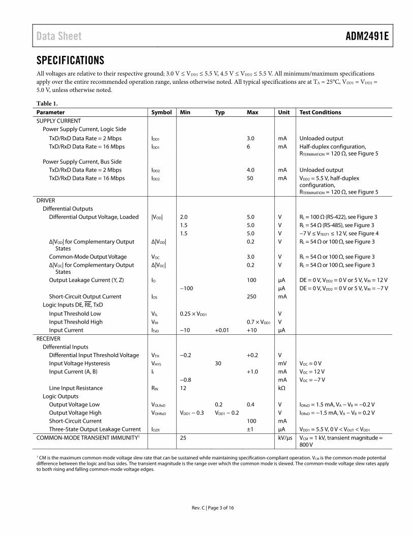
SPECIFICATIONS All voltages are relative to their respective ground; 3.0 V ≤ VDD1 ≤ 5.5 V, 4.5 V ≤ VDD2 ≤ 5.5 V. All minimum/maximum specifications apply over the entire recommended operation range, unless otherwise noted. All typical specifications are at TA = 25°C, VDD1 = VDD2 = 5.0 V, unless otherwise noted.
Table 1. Parameter Symbol Min Typ Max Unit Test Conditions SUPPLY CURRENT
Power Supply Current, Logic Side
TxD/RxD Data Rate = 2 Mbps IDD1 3.0 mA Unloaded output TxD/RxD Data Rate = 16 Mbps IDD1 6 mA Half-duplex configuration,
RTERMINATION = 120 Ω, see Figure 5 Power Supply Current, Bus Side
TxD/RxD Data Rate = 2 Mbps IDD2 4.0 mA Unloaded output TxD/RxD Data Rate = 16 Mbps IDD2 50 mA VDD2 = 5.5 V, half-duplex
configuration, RTERMINATION = 120 Ω, see Figure 5
DRIVER Differential Outputs
Differential Output Voltage, Loaded |VOD| 2.0 5.0 V RL = 100 Ω (RS-422), see Figure 3
1.5 5.0 V RL = 54 Ω (RS-485), see Figure 3 1.5 5.0 V −7 V ≤ VTEST1 ≤ 12 V, see Figure 4
∆|VOD| for Complementary Output States
∆|VOD| 0.2 V RL = 54 Ω or 100 Ω, see Figure 3
Common-Mode Output Voltage VOC 3.0 V RL = 54 Ω or 100 Ω, see Figure 3
∆|VOC| for Complementary Output States
∆|VOC| 0.2 V RL = 54 Ω or 100 Ω, see Figure 3
Output Leakage Current (Y, Z) IO 100 μA DE = 0 V, VDD2 = 0 V or 5 V, VIN = 12 V −100 μA DE = 0 V, VDD2 = 0 V or 5 V, VIN = −7 V Short-Circuit Output Current IOS 250 mA
Logic Inputs DE, RE, TxD
Input Threshold Low VIL 0.25 × VDD1 V Input Threshold High VIH 0.7 × VDD1 V Input Current ITxD −10 +0.01 +10 μA
RECEIVER Differential Inputs
Differential Input Threshold Voltage VTH −0.2 +0.2 V Input Voltage Hysteresis VHYS 30 mV VOC = 0 V Input Current (A, B) II +1.0 mA VOC = 12 V −0.8 mA VOC = −7 V Line Input Resistance RIN 12 kΩ
Logic Outputs Output Voltage Low VOLRxD 0.2 0.4 V IORxD = 1.5 mA, VA − VB = −0.2 V
Output Voltage High VOHRxD VDD1 − 0.3 VDD1 − 0.2 V IORxD = −1.5 mA, VA − VB = 0.2 V
Short-Circuit Current 100 mA Three-State Output Leakage Current IOZR ±1 μA VDD1 = 5.5 V, 0 V < VOUT < VDD1
COMMON-MODE TRANSIENT IMMUNITY1 25 kV/μs VCM = 1 kV, transient magnitude = 800 V
1 CM is the maximum common-mode voltage slew rate that can be sustained while maintaining specification-compliant operation. VCM is the common-mode potential difference between the logic and bus sides. The transient magnitude is the range over which the common mode is slewed. The common-mode voltage slew rates apply to both rising and falling common-mode voltage edges.
ADM2491E Data Sheet
Rev. C | Page 4 of 16
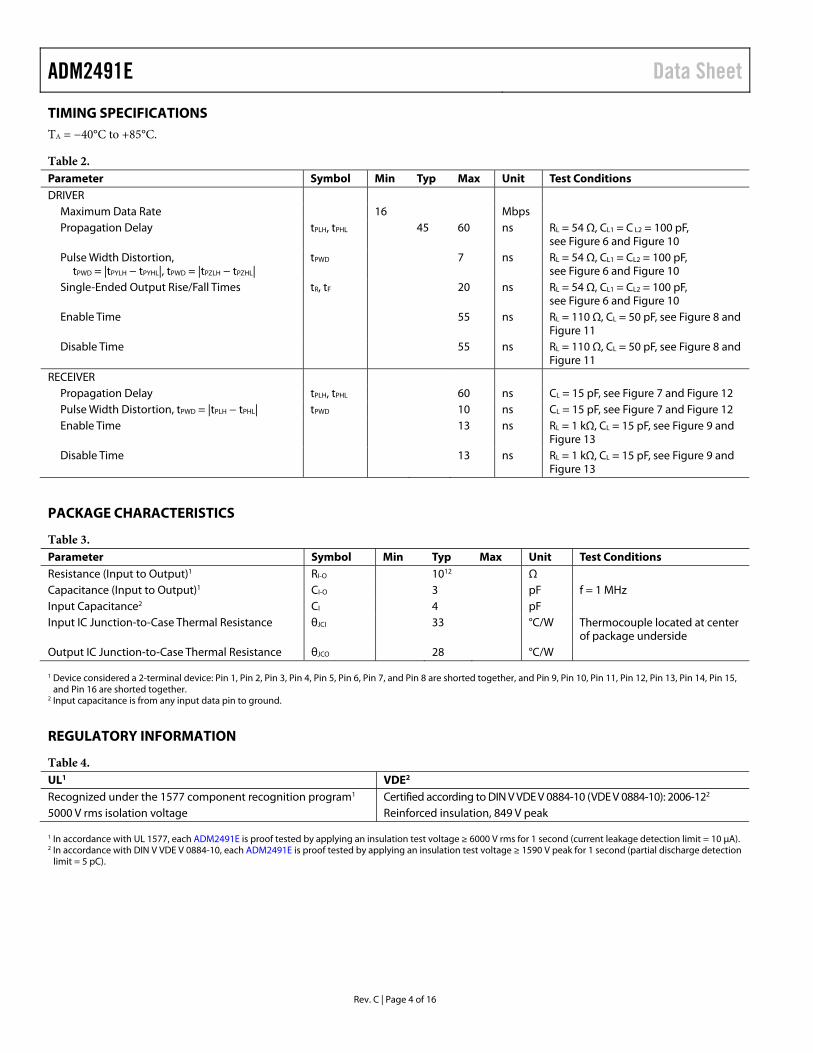
TIMING SPECIFICATIONS TA = −40°C to +85°C.
Table 2. Parameter Symbol Min Typ Max Unit Test Conditions DRIVER
Maximum Data Rate 16 Mbps Propagation Delay tPLH, tPHL 45 60 ns RL = 54 Ω, CL1 = C L2 = 100 pF,
see Figure 6 and Figure 10 Pulse Width Distortion,
tPWD = |tPYLH − tPYHL|, tPWD = |tPZLH − tPZHL| tPWD 7 ns RL = 54 Ω, CL1 = CL2 = 100 pF,
see Figure 6 and Figure 10 Single-Ended Output Rise/Fall Times tR, tF 20 ns RL = 54 Ω, CL1 = CL2 = 100 pF,
see Figure 6 and Figure 10 Enable Time 55 ns RL = 110 Ω, CL = 50 pF, see Figure 8 and
Figure 11 Disable Time 55 ns RL = 110 Ω, CL = 50 pF, see Figure 8 and
Figure 11 RECEIVER
Propagation Delay tPLH, tPHL 60 ns CL = 15 pF, see Figure 7 and Figure 12 Pulse Width Distortion, tPWD = |tPLH − tPHL| tPWD 10 ns CL = 15 pF, see Figure 7 and Figure 12 Enable Time 13 ns RL = 1 kΩ, CL = 15 pF, see Figure 9 and
Figure 13 Disable Time 13 ns RL = 1 kΩ, CL = 15 pF, see Figure 9 and
Figure 13
PACKAGE CHARACTERISTICS
Table 3. Parameter Symbol Min Typ Max Unit Test Conditions Resistance (Input to Output)1 RI-O 1012 Ω Capacitance (Input to Output)1 CI-O 3 pF f = 1 MHz Input Capacitance2 CI 4 pF Input IC Junction-to-Case Thermal Resistance θJCI 33 °C/W Thermocouple located at center
of package underside Output IC Junction-to-Case Thermal Resistance θJCO 28 °C/W 1 Device considered a 2-terminal device: Pin 1, Pin 2, Pin 3, Pin 4, Pin 5, Pin 6, Pin 7, and Pin 8 are shorted together, and Pin 9, Pin 10, Pin 11, Pin 12, Pin 13, Pin 14, Pin 15,
and Pin 16 are shorted together. 2 Input capacitance is from any input data pin to ground.
REGULATORY INFORMATION
Table 4. UL1 VDE2 Recognized under the 1577 component recognition program1 Certified according to DIN V VDE V 0884-10 (VDE V 0884-10): 2006-122 5000 V rms isolation voltage Reinforced insulation, 849 V peak 1 In accordance with UL 1577, each ADM2491E is proof tested by applying an insulation test voltage ≥ 6000 V rms for 1 second (current leakage detection limit = 10 μA). 2 In accordance with DIN V VDE V 0884-10, each ADM2491E is proof tested by applying an insulation test voltage ≥ 1590 V peak for 1 second (partial discharge detection
limit = 5 pC).
Data Sheet ADM2491E
Rev. C | Page 5 of 16
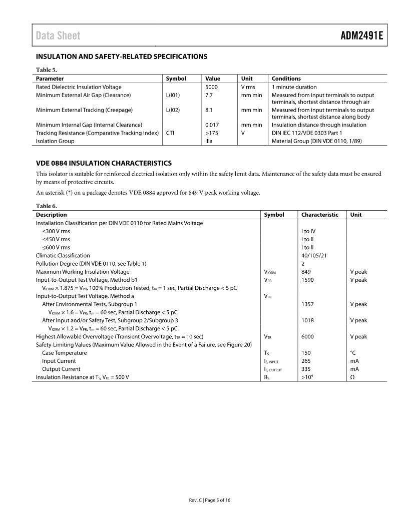
INSULATION AND SAFETY-RELATED SPECIFICATIONS
Table 5. Parameter Symbol Value Unit Conditions Rated Dielectric Insulation Voltage 5000 V rms 1 minute duration Minimum External Air Gap (Clearance) L(I01) 7.7 mm min Measured from input terminals to output
terminals, shortest distance through air Minimum External Tracking (Creepage) L(I02) 8.1 mm min Measured from input terminals to output
terminals, shortest distance along body Minimum Internal Gap (Internal Clearance) 0.017 mm min Insulation distance through insulation Tracking Resistance (Comparative Tracking Index) CTI >175 V DIN IEC 112/VDE 0303 Part 1 Isolation Group IIIa Material Group (DIN VDE 0110, 1/89)
VDE 0884 INSULATION CHARACTERISTICS This isolator is suitable for reinforced electrical isolation only within the safety limit data. Maintenance of the safety data must be ensured by means of protective circuits.
An asterisk (*) on a package denotes VDE 0884 approval for 849 V peak working voltage.
Table 6. Description Symbol Characteristic Unit Installation Classification per DIN VDE 0110 for Rated Mains Voltage
≤300 V rms I to IV ≤450 V rms I to II ≤600 V rms I to II
Climatic Classification 40/105/21 Pollution Degree (DIN VDE 0110, see Table 1) 2 Maximum Working Insulation Voltage VIORM 849 V peak Input-to-Output Test Voltage, Method b1 VPR 1590 V peak
VIORM × 1.875 = VPR, 100% Production Tested, tm = 1 sec, Partial Discharge < 5 pC Input-to-Output Test Voltage, Method a VPR
After Environmental Tests, Subgroup 1 1357 V peak VIORM × 1.6 = VPR, tm = 60 sec, Partial Discharge < 5 pC
After Input and/or Safety Test, Subgroup 2/Subgroup 3 1018 V peak VIORM × 1.2 = VPR, tm = 60 sec, Partial Discharge < 5 pC
Highest Allowable Overvoltage (Transient Overvoltage, tTR = 10 sec) VTR 6000 V peak Safety-Limiting Values (Maximum Value Allowed in the Event of a Failure, see Figure 20)
Case Temperature TS 150 °C Input Current IS, INPUT 265 mA Output Current IS, OUTPUT 335 mA
Insulation Resistance at TS, VIO = 500 V RS >109 Ω
ADM2491E Data Sheet
Rev. C | Page 6 of 16
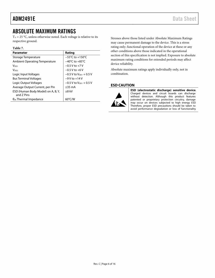
ABSOLUTE MAXIMUM RATINGS TA = 25 °C, unless otherwise noted. Each voltage is relative to its respective ground.
Table 7. Parameter Rating Storage Temperature −55°C to +150°C Ambient Operating Temperature −40°C to +85°C VDD1 −0.5 V to +7 V VDD2 −0.5 V to +6 V Logic Input Voltages −0.5 V to VDD1 + 0.5 V Bus Terminal Voltages −9 V to +14 V Logic Output Voltages −0.5 V to VDD1 + 0.5 V Average Output Current, per Pin ±35 mA ESD (Human Body Model) on A, B, Y,
and Z Pins ±8 kV
θJA Thermal Impedance 60°C/W
Stresses above those listed under Absolute Maximum Ratings may cause permanent damage to the device. This is a stress rating only; functional operation of the device at these or any other conditions above those indicated in the operational section of this specification is not implied. Exposure to absolute maximum rating conditions for extended periods may affect device reliability.
Absolute maximum ratings apply individually only, not in combination.
ESD CAUTION
Data Sheet ADM2491E
Rev. C | Page 7 of 16
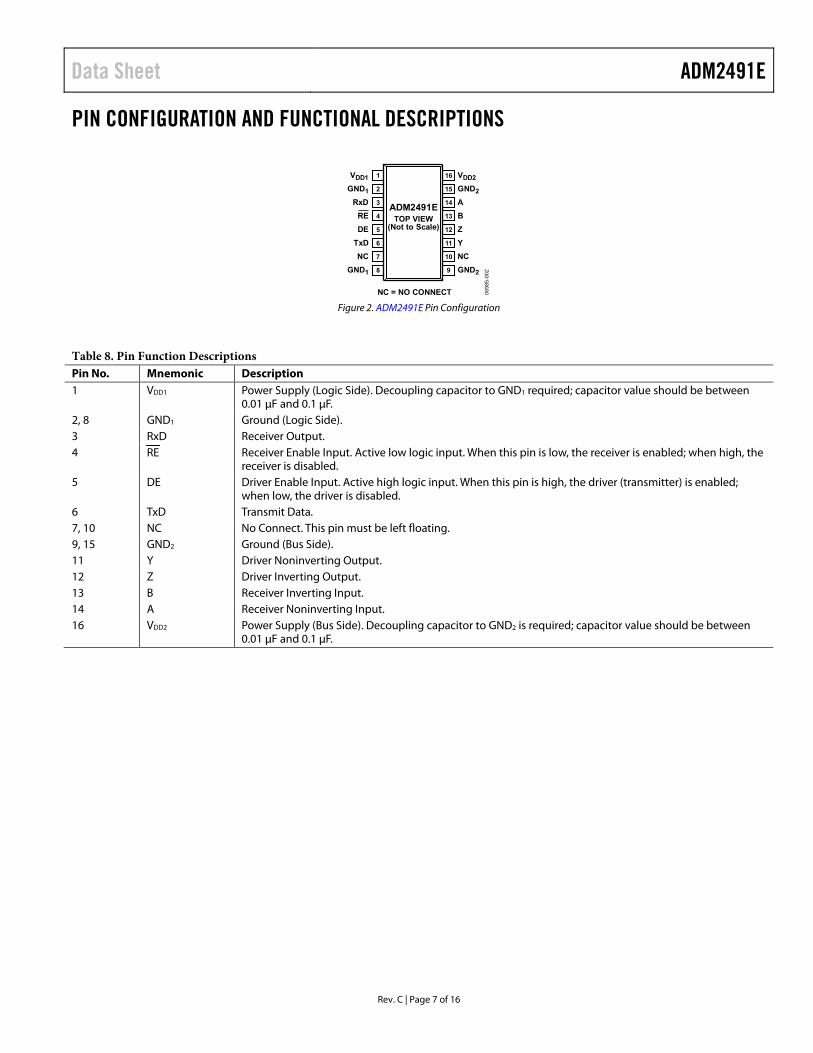
PIN CONFIGURATION AND FUNCTIONAL DESCRIPTIONS
VDD1 1
GND1 2
RxD 3
RE 4
VDD216
GND215
A14
B13
DE 5 Z12
TxD 6 Y11
NC 7 NC10
GND1 8 GND29
NC = NO CONNECT
ADM2491ETOP VIEW
(Not to Scale)
069
85-0
02
Figure 2. ADM2491E Pin Configuration
Table 8. Pin Function Descriptions Pin No. Mnemonic Description 1 VDD1 Power Supply (Logic Side). Decoupling capacitor to GND1 required; capacitor value should be between
0.01 μF and 0.1 μF. 2, 8 GND1 Ground (Logic Side). 3 RxD Receiver Output. 4 RE Receiver Enable Input. Active low logic input. When this pin is low, the receiver is enabled; when high, the
receiver is disabled. 5 DE Driver Enable Input. Active high logic input. When this pin is high, the driver (transmitter) is enabled;
when low, the driver is disabled. 6 TxD Transmit Data. 7, 10 NC No Connect. This pin must be left floating. 9, 15 GND2 Ground (Bus Side). 11 Y Driver Noninverting Output. 12 Z Driver Inverting Output. 13 B Receiver Inverting Input. 14 A Receiver Noninverting Input. 16 VDD2 Power Supply (Bus Side). Decoupling capacitor to GND2 is required; capacitor value should be between
0.01 μF and 0.1 μF.
ADM2491E Data Sheet
Rev. C | Page 8 of 16
TEST CIRCUITS
VOC
VOD
0698
5-00
3
RL2
RL2
Figure 3. Driver Voltage Measurement
60ΩVOD
375Ω
375Ω
VTEST0
6985
-004
Figure 4. Driver Voltage Measurement
VDD1
GND1
A
B
VDD2
GND2
Y
ZTxD
DE
RxD
ADM2491E
069
85-
005
GA
LVA
NIC
IS
OL
AT
ION
RTERMINATION
RE
Figure 5. Supply Current Measurement Test Circuit
CL2
CL1
RLDIFF
Y
Z
069
85-
006
Figure 6. Driver Propagation Delay
CL
VOUT
A
B
0698
5-0
07
Figure 7. Receiver Propagation Delay
069
85-0
08
Y
Z
VCCVOUT
S2S1RL
CL
0V OR 3V
DE
Figure 8. Driver Enable/Disable
0698
5-00
9
ARE
B
VCCVOUT
S2
S1RL
CL
RE IN
+1.5V
–1.5V
Figure 9. Receiver Enable/Disable
Data Sheet ADM2491E
Rev. C | Page 9 of 16
SWITCHING CHARACTERISTICS
1.5V1.5V
tPLH tPHL
tR tF
1/2VOUTVOUT
90% POINT
10% POINT
90% POINT
10% POINT
tPWD = |tPLH – tPHL|
VDD1
0V
Z
Y
VOH
VOL
Y, Z
TxD
06
98
5-0
10
Figure 10. Driver Propagation Delay, Rise/Fall Timing
tZL tLZ
tZH tHZ
0.5VDD10.5VDD1
VOL + 0.5V
VOH – 0.5V
2.3V
2.3V
DE
Y, Z
Y, Z
VDD1
0V
VOL
VOH
0V 069
85-0
11
Figure 11. Driver Enable/Disable Delay
A, B
RxD
0V 0V
1.5V 1.5V
tPLH tPHL
VOH
VOL 0698
5-01
2
Figure 12. Receiver Propagation Delay
tZL tLZ
tZH tHZ
0.5VDD10.5VDD1
VOL + 0.5V
VOH – 0.5V
1.5V
1.5V
RE
RxD
RxD
0V
VDD1
0V
VOL
VOH
0V 0698
5-0
13
OUTPUT LOW
OUTPUT HIGH
Figure 13. Receiver Enable/Disable Delay
ADM2491E Data Sheet
Rev. C | Page 10 of 16
TYPICAL PERFORMANCE CHARACTERISTICS
TEMPERATURE (°C)
I DD
1 S
UP
PLY
CU
RR
EN
T (
mA
)
0698
5-0
14–40 –20 0 20 40 60 80
100Ω LOAD
54Ω LOAD
2.42
2.44
2.46
2.48
2.50
2.52
2.54
2.56
2.58NO LOAD
Figure 14. IDD1 Supply Current vs. Temperature
0
10
20
30
40
50
60
TEMPERATURE (°C) 069
85-0
15–40 –20 0 20 40 60 80
I DD
2 S
UP
PLY
CU
RR
EN
T (
mA
)
NO LOAD
100Ω LOAD
54Ω LOAD
Figure 15. IDD2 Supply Current vs. Temperature
0
10
20
30
40
50
60
–40 –20 0 20 40 60 80
tPYHL
0698
5-0
34
TEMPERATURE (°C)
DE
LA
Y (
ns)
tPZHLtPYLHtPZLH
Figure 16. Driver Propagation Delay vs. Temperature
0
10
20
30
40
50
60
–40 –20 0 20 40 60 80
069
85-0
35
TEMPERATURE (°C)
DE
LA
Y (
ns)
tPLHtPHL
Figure 17. Receiver Propagation Delay vs. Temperature
0698
5-0
32
CH1 2VCH3 2V
CH2 2VCH4 2V
M20ns A CH1 2.32V
1
3
4
T 48ns
∆: 2.12V@: 7.72V
ΩΩ
ΩΩ
TxD
Z
Y
RxD
Figure 18. Driver/Receiver Propagation Delay, Low to High (RLDIFF = 54 Ω, CL1 = CL2 = 100 pF)
069
85-0
33
CH1 2VCH3 2V
CH2 2VCH4 2V
M20ns A CH1 3.24V
1
3
4
T 48ns
∆: 2.12V@: 7.72V
TxD
Z
Y
RxD
ΩΩ
ΩΩ
Figure 19. Driver/Receiver Propagation Delay, High to Low (RLDIFF = 54 Ω, CL1 = CL2 = 100 pF)
Data Sheet ADM2491E
Rev. C | Page 11 of 16
CASE TEMPERATURE (°C)
SA
FE
TY
-LIM
ITIN
G C
UR
RE
NT
(m
A)
00
350
300
250
200
150
100
50
50 100 150 200
SIDE 1
SIDE 2
0698
5-0
20
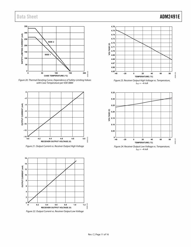
Figure 20. Thermal Derating Curve, Dependence of Safety-Limiting Values with Case Temperature per VDE 0884
–14
–12
–10
–8
–6
–4
–2
0
4.0 4.2 4.4 4.6 4.8 5.0
RECEIVER OUTPUT VOLTAGE (V)
OU
TP
UT
CU
RR
EN
T (
mA
)
069
85-0
21
Figure 21. Output Current vs. Receiver Output High Voltage
0
2
4
6
8
10
12
14
16
0 0.2 0.4 0.6 0.8 1.0 1.2
RECEIVER OUTPUT VOLTAGE (V)
OU
TP
UT
CU
RR
EN
T (
mA
)
069
85-0
22
Figure 22. Output Current vs. Receiver Output Low Voltage
4.65
4.66
4.67
4.68
4.69
4.70
4.71
4.72
4.73
4.74
4.75
4.76
–20–40 0 20 40 60 80
069
85-0
36
TEMPERATURE (°C)
VO
LT
AG
E (
V)
Figure 23. Receiver Output High Voltage vs. Temperature, IRxD = −4 mA
0.05
0.10
0.15
0.20
0.25
0.30
0.35
0–40 –20 0 20 40 60 80
0698
5-03
7
TEMPERATURE (°C)
VO
LT
AG
E (
V)
Figure 24. Receiver Output Low Voltage vs. Temperature, IRxD = –4 mA
ADM2491E Data Sheet
Rev. C | Page 12 of 16
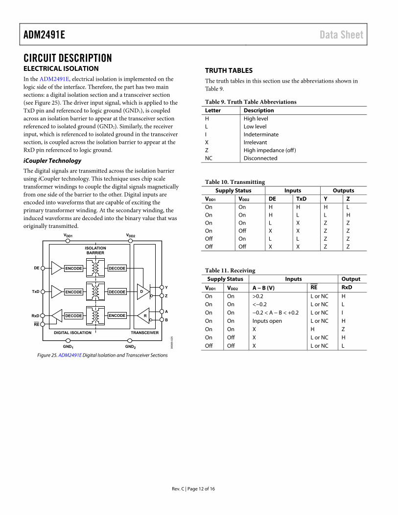
CIRCUIT DESCRIPTION ELECTRICAL ISOLATION In the ADM2491E, electrical isolation is implemented on the logic side of the interface. Therefore, the part has two main sections: a digital isolation section and a transceiver section (see Figure 25). The driver input signal, which is applied to the TxD pin and referenced to logic ground (GND1), is coupled across an isolation barrier to appear at the transceiver section referenced to isolated ground (GND2). Similarly, the receiver input, which is referenced to isolated ground in the transceiver section, is coupled across the isolation barrier to appear at the RxD pin referenced to logic ground.
iCoupler Technology
The digital signals are transmitted across the isolation barrier using iCoupler technology. This technique uses chip scale transformer windings to couple the digital signals magnetically from one side of the barrier to the other. Digital inputs are encoded into waveforms that are capable of exciting the primary transformer winding. At the secondary winding, the induced waveforms are decoded into the binary value that was originally transmitted.
ISOLATIONBARRIER
VDD2VDD1
Y
Z
A
B
GND2GND1
TxD
RxD
RE
ENCODE
DECODE
DECODE
ENCODE
DE DECODEENCODE
D
R
TRANSCEIVER
0698
5-0
25
DIGITAL ISOLATION
Figure 25. ADM2491E Digital Isolation and Transceiver Sections
TRUTH TABLES The truth tables in this section use the abbreviations shown in Table 9.
Table 9. Truth Table Abbreviations Letter Description H High level L Low level I Indeterminate X Irrelevant Z High impedance (off ) NC Disconnected
Table 10. Transmitting Supply Status Inputs Outputs
VDD1 VDD2 DE TxD Y Z On On H H H L On On H L L H On On L X Z Z On Off X X Z Z Off On L L Z Z Off Off X X Z Z
Table 11. Receiving Supply Status Inputs Output
VDD1 VDD2 A − B (V) RE RxD
On On >0.2 L or NC H On On <−0.2 L or NC L
On On −0.2 < A − B < +0.2 L or NC I On On Inputs open L or NC H
On On X H Z On Off X L or NC H
Off Off X L or NC L
Data Sheet ADM2491E
Rev. C | Page 13 of 16
THERMAL SHUTDOWN The ADM2491E contains thermal shutdown circuitry that protects the part from excessive power dissipation during fault conditions. Shorting the driver outputs to a low impedance source can result in high driver currents. The thermal sensing circuitry detects the increase in die temperature under this condition and disables the driver outputs. This circuitry is designed to disable the driver outputs when a die temperature of 150°C is reached. As the device cools, the drivers are re-enabled at a temperature of 140°C.
FAIL-SAFE RECEIVER INPUTS The receiver inputs include a fail-safe feature that guarantees a logic high on the RxD pin when the A and B inputs are floating or open circuited.
MAGNETIC FIELD IMMUNITY Because iCoupler devices use a coreless technology, no magnetic components are present and the problem of magnetic saturation of the core material does not exist. Therefore, iCoupler devices have essentially infinite dc field immunity. The following analysis defines the conditions under which this may occur. The 3 V operating condition of the ADM2491E is examined because it represents the most susceptible mode of operation.
The limitation on the ac magnetic field immunity of the iCoupler is set by the condition that induced an error voltage in the receiving coil (the bottom coil in this case) that was large to either falsely set or reset the decoder. The voltage induced across the bottom coil is given by
2
nrdtdβ
V ; Nn ,...,2,1
where (if the pulses at the transformer output are greater than 1.0 V in amplitude): β is the magnetic flux density (gauss). N is the number of turns in the receiving coil. rn is the radius of the nth turn in the receiving coil (cm).
The decoder has a sensing threshold of about 0.5 V; therefore, there is a 0.5 V margin in which induced voltages can be tolerated.
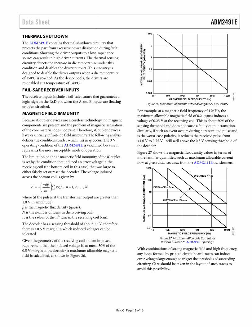
Given the geometry of the receiving coil and an imposed requirement that the induced voltage is, at most, 50% of the 0.5 V margin at the decoder, a maximum allowable magnetic field is calculated, as shown in Figure 26.
MAGNETIC FIELD FREQUENCY (Hz)
1k 10k 100k 100M1M 10M
100
10
1
0.1
0.01
0.001
MA
XIM
UM
AL
LO
WA
BL
E M
AG
NE
TIC
FL
UX
DE
NS
ITY
(kG
AU
SS
)
069
85-0
26
Figure 26. Maximum Allowable External Magnetic Flux Density
For example, at a magnetic field frequency of 1 MHz, the maximum allowable magnetic field of 0.2 kgauss induces a voltage of 0.25 V at the receiving coil. This is about 50% of the sensing threshold and does not cause a faulty output transition. Similarly, if such an event occurs during a transmitted pulse and is the worst-case polarity, it reduces the received pulse from >1.0 V to 0.75 V—still well above the 0.5 V sensing threshold of the decoder.
Figure 27 shows the magnetic flux density values in terms of more familiar quantities, such as maximum allowable current flow, at given distances away from the ADM2491E transformers.
MAGNETIC FIELD FREQUENCY (Hz)
1k 10k 100k 100M1M 10M
DISTANCE = 1m
DISTANCE = 100mm
DISTANCE = 5mm
1000
100
0.1
1
10
0.01
MA
XIM
UM
AL
LO
WA
BL
E C
UR
RE
NT
(kA
)
0698
5-0
27
Figure 27. Maximum Allowable Current for
Various Current-to-ADM2491E Spacings
With combinations of strong magnetic field and high frequency, any loops formed by printed circuit board traces can induce error voltages large enough to trigger the thresholds of succeeding circuitry. Care should be taken in the layout of such traces to avoid this possibility.
ADM2491E Data Sheet
Rev. C | Page 14 of 16
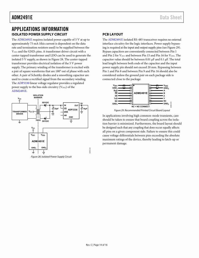
APPLICATIONS INFORMATION ISOLATED POWER SUPPLY CIRCUIT The ADM2491E requires isolated power capable of 5 V at up to approximately 75 mA (this current is dependent on the data rate and termination resistors used) to be supplied between the VDD2 and the GND2 pins. A transformer driver circuit with a center-tapped transformer and LDO can be used to generate the isolated 5 V supply, as shown in Figure 28. The center-tapped transformer provides electrical isolation of the 5 V power supply. The primary winding of the transformer is excited with a pair of square waveforms that are 180° out of phase with each other. A pair of Schottky diodes and a smoothing capacitor are used to create a rectified signal from the secondary winding. The ADP3330 linear voltage regulator provides a regulated power supply to the bus-side circuitry (VDD2) of the ADM2491E.
ISOLATIONBARRIER
VCC
78253 SD103C
SD103C
22µF 10µF
5VOUTIN
SD
ERR
NRGND
VCC
VDD1 VDD2
GND1 GND2
ADP3330
ADM2491E
06
98
5-0
28
TRANSFORMERDRIVER
VCC
++
Figure 28. Isolated Power Supply Circuit
PCB LAYOUT The ADM2491E isolated RS-485 transceiver requires no external interface circuitry for the logic interfaces. Power supply bypass-ing is required at the input and output supply pins (see Figure 29). Bypass capacitors are conveniently connected between Pin 1 and Pin 2 for VDD1 and between Pin 15 and Pin 16 for VDD2. The capacitor value should be between 0.01 μF and 0.1 μF. The total lead length between both ends of the capacitor and the input power supply pin should not exceed 20 mm. Bypassing between Pin 1 and Pin 8 and between Pin 9 and Pin 16 should also be considered unless the ground pair on each package side is connected close to the package.
VDD1GND1
RxDREDE
TxDNC
GND1
VDD2GND2AB
NC
ZY
GND2
NC = NO CONNECT
ADM2491E
0698
5-0
29
Figure 29. Recommended Printed Circuit Board Layout
In applications involving high common-mode transients, care should be taken to ensure that board coupling across the isola-tion barrier is minimized. Furthermore, the board layout should be designed such that any coupling that does occur equally affects all pins on a given component side. Failure to ensure this could cause voltage differentials between pins exceeding the absolute maximum ratings of the device, thereby leading to latch-up or permanent damage.
Data Sheet ADM2491E
Rev. C | Page 15 of 16
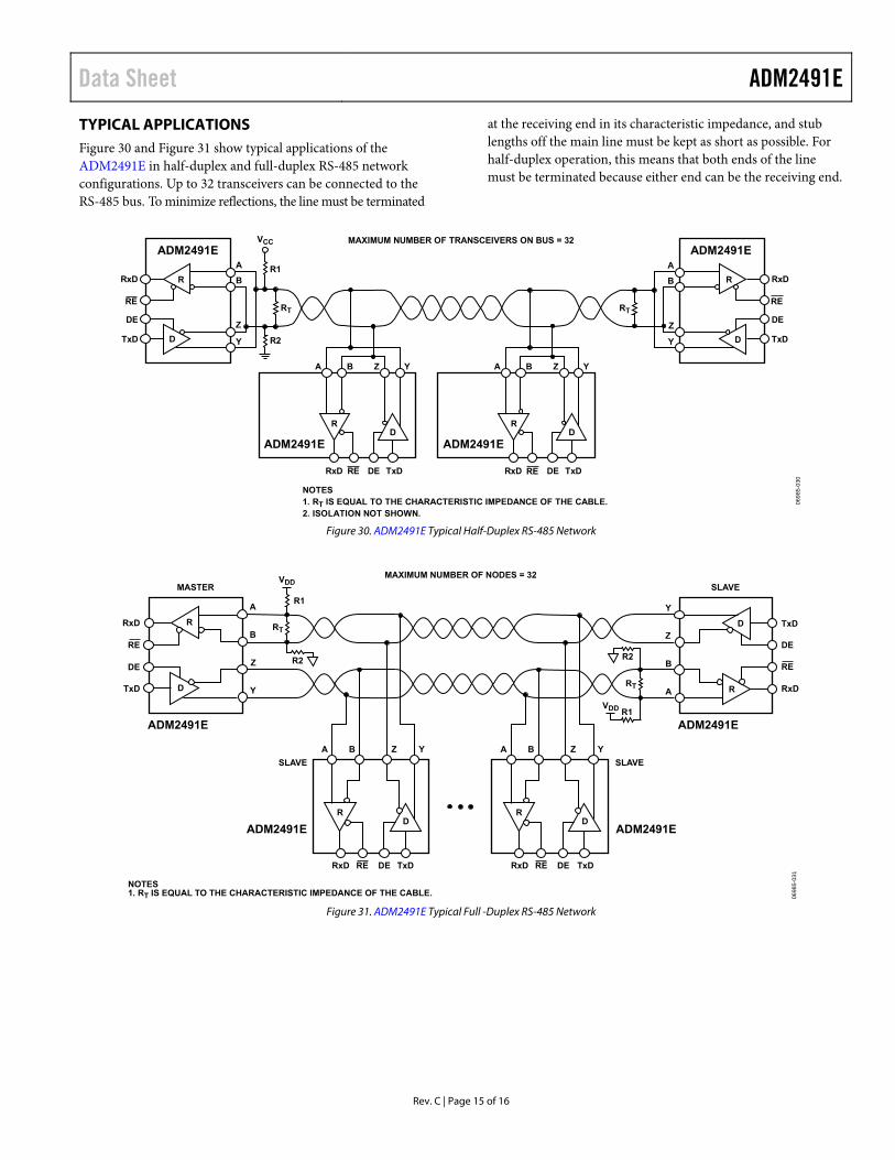
TYPICAL APPLICATIONS Figure 30 and Figure 31 show typical applications of the ADM2491E in half-duplex and full-duplex RS-485 network configurations. Up to 32 transceivers can be connected to the RS-485 bus. To minimize reflections, the line must be terminated
at the receiving end in its characteristic impedance, and stub lengths off the main line must be kept as short as possible. For half-duplex operation, this means that both ends of the line must be terminated because either end can be the receiving end.
NOTES1. RT IS EQUAL TO THE CHARACTERISTIC IMPEDANCE OF THE CABLE.2. ISOLATION NOT SHOWN.
069
85-0
30
ADM2491E
RxD DE TxD
A B Z Y
ADM2491E
RxD DE TxD
A B Z Y
ADM2491EADM2491EA
B
Z
Y
A
B
Z
Y
R1
R2
RT
VCC
RD
RD
R
D
R
D
RT
RxD
DE
TxD
RxD
DE
TxD
MAXIMUM NUMBER OF TRANSCEIVERS ON BUS = 32
RERE
RE RE
Figure 30. ADM2491E Typical Half-Duplex RS-485 Network
0698
5-0
31
R
D
RxD
RE
TxD
DE
ADM2491E
ADM2491E
A
B
Z
Y
RD
RxD TxDDE
A B Z Y
RE
R
D
RxD
TxD
DE
ADM2491E
MASTER SLAVE
SLAVE
A
B
Z
Y
RE
MAXIMUM NUMBER OF NODES = 32
ADM2491E
RD
RxD TxDDE
A B Z Y
RE
SLAVE
NOTES1. RT IS EQUAL TO THE CHARACTERISTIC IMPEDANCE OF THE CABLE.
RT
VDD
R1
R2
RT
VDD R1
R2
Figure 31. ADM2491E Typical Full -Duplex RS-485 Network
ADM2491E Data Sheet
Rev. C | Page 16 of 16
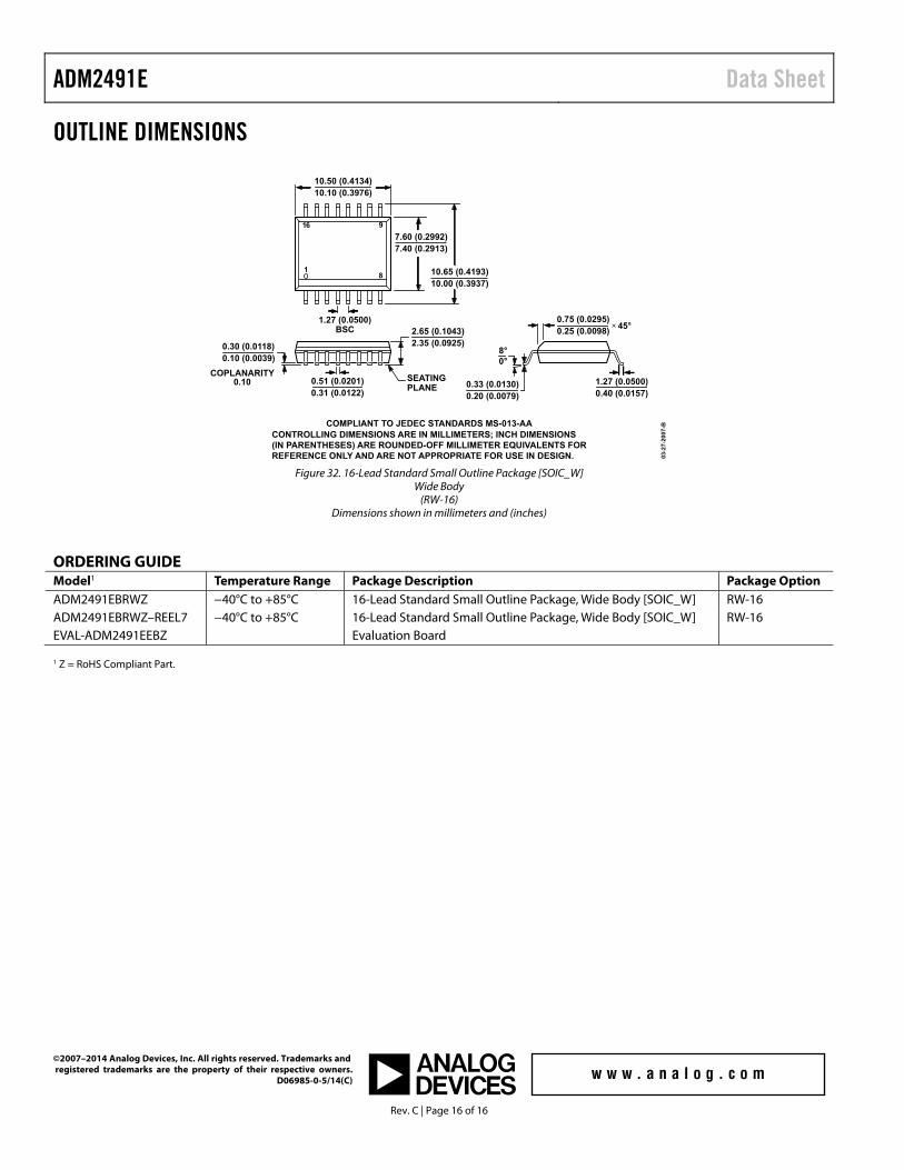
OUTLINE DIMENSIONS
CONTROLLING DIMENSIONS ARE IN MILLIMETERS; INCH DIMENSIONS(IN PARENTHESES) ARE ROUNDED-OFF MILLIMETER EQUIVALENTS FORREFERENCE ONLY AND ARE NOT APPROPRIATE FOR USE IN DESIGN.
COMPLIANT TO JEDEC STANDARDS MS-013-AA
10.50 (0.4134)10.10 (0.3976)
0.30 (0.0118)0.10 (0.0039)
2.65 (0.1043)2.35 (0.0925)
10.65 (0.4193)10.00 (0.3937)
7.60 (0.2992)7.40 (0.2913)
0.75 (0.0295)0.25 (0.0098)
45°
1.27 (0.0500)0.40 (0.0157)
COPLANARITY0.10 0.33 (0.0130)
0.20 (0.0079)
0.51 (0.0201)0.31 (0.0122)
SEATINGPLANE
8°0°
16 9
81
1.27 (0.0500)BSC
03-2
7-20
07-B
Figure 32. 16-Lead Standard Small Outline Package [SOIC_W]
Wide Body (RW-16)
Dimensions shown in millimeters and (inches)
ORDERING GUIDE Model1 Temperature Range Package Description Package Option ADM2491EBRWZ −40°C to +85°C 16-Lead Standard Small Outline Package, Wide Body [SOIC_W] RW-16 ADM2491EBRWZ–REEL7 −40°C to +85°C 16-Lead Standard Small Outline Package, Wide Body [SOIC_W] RW-16 EVAL-ADM2491EEBZ Evaluation Board 1 Z = RoHS Compliant Part.
©2007–2014 Analog Devices, Inc. All rights reserved. Trademarks and registered trademarks are the property of their respective owners. D06985-0-5/14(C)